Embed Size (px)
Citation preview
General Disclaimer
One or more of the Following Statements may affect this Document
This document has been reproduced from the best copy furnished by the
organizational source. It is being released in the interest of making available as
much information as possible.
This document may contain data, which exceeds the sheet parameters. It was
furnished in this condition by the organizational source and is the best copy
available.
This document may contain tone-on-tone or color graphs, charts and/or pictures,
which have been reproduced in black and white.
This document is paginated as submitted by the original source.
Portions of this document are not fully legible due to the historical nature of some
of the material. However, it is the best reproduction available from the original
submission.
Produced by the NASA Center for Aerospace Information (CASI)
https://ntrs.nasa.gov/search.jsp?R=19830026325 2020-05-13T02:55:32+00:00Z
Final Report for NAG-1-174:
Chip Level Simulation of Fault Tolerant Computers
Performance PeriodJune 1,1981 - May 31,1983
J. R. Armstrong
Electrical Engineering DepartmentVirginia Tech
Blacksburg,Va. 24061
t
t
INTRODUCTION
The purpose of this report is to give the results ofresearch carried out under Grant NAG-1-174, "Chip Level Sim-ulation of Fault Tolerant Computers". The grant performanceperiod was June 1,1981 through May 31,1983. This particulardocument summarizes the work that has been performed duringthis period. The work is described in detail in variouspapers and reports, copies of which have been transmitted toNASA along with this document.
BACKGROUND
The advent of LSI and VLSI circuits has led to increased useof functional level modeling and simulation. This is due tothe tremendous complexity of these devices which causesgreat problems of scale for traditional gate level modelingand simulation techniques. LSI devices contain thousands ofgates and gate level simulation of systems containing suchdevices can be prohibitively expensive. Moreover, the gatelevel models of these devices are usually known only to themanufacturer and he is generally unwilling to release thisproprietary information. And finally, as we envision thedigital systems of the future as being composed of many LSIdevices interconnected in complex ways, it is important thatlevels of representation are developed that are accurate butstill involve a manageable amount of detail.
During the past four years at the Electrical EngineeringDepartment of VPI, we have developed a form of functionalsimulation which we refer to as "chip level" simulation[1,2]. Modeling at the chip level involves modeling theinternal device micro-operations as well as detailed inter-face timing without employing a gate level description ofthe device. This approach to modeling and simulation hasbeen implemented in a system called GSP (General Simulatior.Program). GSP has been employed for device modeling researc:nsponsored by the Naval Surface Weapons Center [3], the RomeAir Development Center [4], and the NASA Langley ResearchCenter under NASA Grant NAG 1-174 and has been shown to bean effective system for the modeling and simulation of I,SIdevices.
In addition to the work outlined above, GSP will also beused to develop functional fault modeling techniques and adefinition of functional fault coverage under a grant fromIBM.
t
z
SUMMARY OF WORK CARRIED OUT UNDER NAG 1-174
During the performance period of NAG 1-174 our efforts havebeen divided into four major areas: (1) development of chiplevel modeling techniques. (2) modeling of a fault tolerantcomputer (SIFT). (3) development of an efficient approach tofunctional fault simulation. (4) simulation software devel-opment. (5) development of a high level Language version ofGSP possessing increased simulation efficiency. (6) devel-opment of a parallel architecture for functional simulation.
CHIP LEVEL MODELING TECHNIQUES
Our experience in modeling on a previous Air Force sponsoredcontract [4] and that gained during the present work hasresulted in the development of various techniques for model-ing LSI devices. In order to preserve this information forothers wishing to engage in chip level modeling, during thefirst year of NAG 1-174, we prepared a document entitled"Chip Level Modeling Techniques" [6]. This document illus-trates basic techniques for the modeling of the sequentialand combinational logic aspects of LSI logic circuits. Inaddition, methods are presented for the accurate modeling ofdevice interface timing, i.e. methods are given for modelingsuch input timing specifications as set up time,hold timeand minimum pulse width. These basic techniques are thenused to illustrate the modeling of devices peculiar tomicLoprocessor systems. The document represents our attemptto define for the unsophisticated device modeler techniquesthat he can use to model devices effectively. The originaldocument was submitted to NASA as part of the first annualreport for NAG 1-174 on May 31, 1982, but we have continuedto make corrections and additions to it since then. A copyof the revised version accompanies this report.
In addition to the above report, a journal article was pre-pared covering material in the some area. The article, enti-tled "Chip Level Modeling and Simulation", will appear thiscoming October in the journal Simulation.
trr
I
2
t
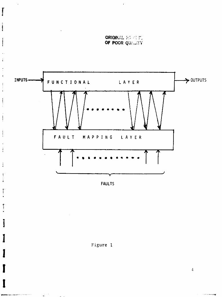
During the second year of NAG 1-174, we attempted to definethe generic nature of a good functional model. In doing so,we developed a two layered approach to functional modeling.Figure 1 shows the two layered model structure. The top lay-er, the functional layer, reproduces the input/output behav-ior of the LSI device. This layer consists of a network ofcomputational nodes which are interconnected in such a man-ner as to simulate the major signal paths in the modeleddevice. If one is interested in producing the behavior ofthe good device only, as is the case where the simulation isto be used for design verification or an automatic testerapplication, then this is the only layer that is necessary.However, if fault modeling is desired, then an additionallayer is required to perform the mapping of physical fault,onto the functional layer.
The concept of the fault mapping layer is built on the ideathat in a chip level model of an LSI device, themicro-operations that comprise the model are themselves com-posed of micro-operations of smaller blocks of logic. To addthe fault mapping layer, one codes the micro-operations ofthese blocks of logic in subroutine form. These subrou-tines are then called by the functional layer to implementthe micro-operations of the chip level model. The faultinjection process is thus simplified in that one need onlydetermine the effect that fault has on the individual sub-routines. 7 n implementing our models in this fashion, wehave found that it is better to represent these functionallogic blocks, e.g. an ALU, as a group of subroutines asopposed to one large subroutine in order to alleviate theproblem of passing a large number of parameters. The use ofthe fault mapping layer alleviates the problem of"micro-operation scatter" which troubled us in some of ourearly fault modeling efforts. This approach was used to mod-el the BDX-930 processor. In this case, a group ofsubroutines was used to represent each LSI or MSI chip inthe design. For the VLSI devices now being built, genericlogic structures on these devices, such as PLAs, gatearrays, and programmable logic cells will be represented assubroutines.
This modeling structure is fully described in a paper enti-tled "Chip Level Modeling of LSI Devices" which was submit-ted to the IEEE Transactions on Computer Aided Design ofIntegrated Circuits and is currently in the review process.
Other systematic approaches to modeling are given in "Func-tional Level Modeling of Digital Devices", a masters thesiswritten by Venugopal Puthenpurayil, one of the graduateresearch assistants during the first year of the project. Hedeveloped the CPU/Timing model for the BDX-930 processorwhich is described in the next section.
4
L--- _
OUTPUTS
B) Modeling the Sift Computer
As SIFT consists of a number of BDX-930rocessors modeling9of the BDX-930 formed the first phase of the modeling proce-dure. Originally we broke the BDX-930 , which is a bit sliceprocessor built from MSI and LSI devices, down into fourfunctional models: processor, timing and control, memory,and broadcast and recieve logic. However as the models werecompleted and tested together, it became apparent that hav-ing the timing and control circuit model separate created agreat deal of time queue activity which was unnecessary interms of the goals of the simulation and which also greatlyeffected the efficiency of the simulation. Because of this,we merged the timing and control circuit with the CPU model.The effect of this and other improvements to the CPU modelwas to effectively double the efficiency of the model. Inaddition to this, the VA. Tech Computer Center recantlyinstalled an IBM 3081 dual processor sytem which is a 5 MIPmachine. The overall effect of this was to make the CPU mod-el run at an efficiency of 100 processor clock pulses perhost CPU second.
The present status of the SIFT modeling effort is asfollows: All models have been coded and checked out. TheCPU/Timing and Control model and the Broadcast and ReceiveLogic model, in particular, were subjected to three monthsof intensive testing.
In doing the modeling described above, a great amount ofeffort had to be expended in defining the timing of theinterface signals. Most of this timing information was com-piled from the timing specifications of individual chips.The timing information for the CPU and timing and controllogic is given in the report "Modeling the BDX-930" whichwas previously submitted to NASA. Additonal information isalso contained in Venugopal"s thesis (described in the pre-vious section).
tThroughout the modeling process, particular importance wasgiven to modeling so that fault injection was straight for-ward. This was especially so in the case of the CPU, where acarefully constructed two layer model was developed (seeprevious discussion).
' The modeling process was completed with approximately 5months remaining on the grant period. The decision was madeto apply the remaining resources to the development of thehigh level version of GSP and the parallel architecture for'functional simulation( described below). As a result no sys-tem level fault simulations were performed. However the
' models areeffort we
available and should NASA lesire to resumecould do so.
this
r
1
1
EFFICIENT APPROACH TO FUNCTIONAL FAULT SIMULATION
While we 'feel that the use of functional simulation is anecessity for LSI systems, it is tine that the simulation offaults at the functional level is not as straight forward asthe gate level fault simulation process. In gate level faultsimulation one merely causes a gate input or output to bestuck at one or stuck at zero and then simulates the fault.In using functional simulation, the fault insertion processis more complex in that if one is going to insert the faultinternal to the chip, one must modify the functional modelof the chip. The two layer model discussed in the previoussection should ease this process. However there is an add-
tional problem that must be addressed. The variety of faulttypes, e.g. micro-operation faults, register stuck atfaults, control faults, timing faults etc., dictates asophisticated approach to the insertion process. This bringsin to question the basic time efficiency of the functionalfault insertion process, i.e. how many .`aults per unit timecan be inserted and fault runs made. It is true that in gen-eral a functional fault will cover a fairly large number ofgate faults but one must still be concerned with making thefuntional fault insertion process as efficient as possible.
In response to these problems we've devoted considerableeffort during the performance period to development of func-tional fault insertion techniques and also to the develop-ment of system level approaches to allow efficientfunctional fault simulation. This work was carried out byShirish Sathe, one of the graduate research assistants onthe project. The results of this work are given in his mas-ter's thesis, "Functional Fault Simulaton for LSI Devices",which we have previously submitted to NASA. The thesisdescribes fault insertion techniques for the following typesof faults: faulty micro-operations,timing faults, stuck atfaults in internal device memory, interconnect faults (bothstuck ats and shorts between lines), and transient faults.In addiion to these fundamental techniques, the thesisdescribes a method for structuring the model to make thefault insertion process easier and to also allow a closertie between real chip defects and functional faults. (Thefault mapping layer described above.) Also presented aremethods for imbedding faults in models of good devices whichcan be invoked by means of external control signals to occurany time during a simulation run.
In order to perform the actual fault simulationsefficiently, we have developed a software system whichtotally decouples the fault insertion process from the actu-al simulation process. The user prepares faulty models inone environment and then can submitt a whole series of faultruns as a single entity. The complete series of fault runswill run to completion without operator intervention withspecified simulation data being recorded for each run.
Several other features have also been developed to aid inthe fault insertion process. In the GSP simulation system,the interconnect between simulated chips is contained in acommand file. An efficient method of inserting interconnectfaults is to modify the good command file to create one mod-eling the faulty interconnect. An automatic technique hasbeen devloped for the preparation of these files. The userneed only specify the module in the system at whose inter-face he wishes to insert faults. A program willautomatically create an interconnect file for each stuck atfault for the specified chip ,thus releaving the user of anerror prone editing task, and saving considerable time.
Another feature has been added to facilitate the modeling oftiming problems. Timing faults can of course be inserted bymodification of the delay control parameters in the individ-ual models as part of the fault insertion process describedabove. In addition to this however, a timing jitter optionhas been added which can be invoked during the actual simu-lation. With this feature, a pseudoramdom bias of aspecified range, e.g. 20%, is added to each scheduled signalevent, thus allowing the testing of system timing margins.
All of the features discussed above are described in detailin Mr. Sathe's thesis. The sum total of this work providestools for carrying out a meaningful and efficient functionalfault simulation process.
-1SIMULATION SOFTWARE DEVELOPMENT
During the grant period, a number of important softwaredevelopment tasks have been carried out as an adjunct to ourbasic research activities. First, the GSP simulation systemwas installed on the Cyber 173 computer at NASA- Langley anda VAX 11-780 at Va. Tech. This is of course in addition toits normal operation on the IBM system at Va. Tech.Secondly, we have made modifications to the human interfaceof the system in order to make it easier to use. In partic-ular, better mnemonics were chcsen for existing modelinglanguage instructions and several new instructions were add-ded to account for some newly discovered modelingsituations. These changesGSP user's guide which has
have been reflected in a updatedbeen previously transmitted to
NASA.
' During the second year of NAG-1-174, we converted theBDX-930 cross-assembler and linking loader to allow it torun on the VAX 11-780.
iThe conversion activities relating to the VAX 11-780 wereconsidered important in light of the proposed AIRLAB envi-ronment.
_ _yam
I^
a
I
A recent activitiy, actually begun after th,a termination ofthe grant period, involves the conversion of the presentversion of GSP to run on a personal computer with a rela-tively large memory space. It is expected that this conver-sion process will be completed this fall.
IDEMOPMENT OF A MORE EFFICIENT , HIGH LEVEL VERSION OF GSP
The current version of GSP runs too slowly for man gy{ applica-tions, such as a complete simulation of the SIFT executivesoftware. In order to improve simulation speed, hopefully bya factor of 100 or greater, the simulator was redesigned tobe directly executable on the DEC VAX-11. In the currentversion, the hardware description language is translatedinto an integer microcode language, which is interpreted atrun-time by the FORTRAN simulator program. This intermediatetranslation was eliminated by compiling the moduledescription directly into VAX-11 object code routines exe-cuted by the assembly-coded simulator. This should providea significant speedup.
The modeling language was also redesigned to be more power-ful and support structured programming techniques. Theassembly-like language was replaced with a high-level blockstructured language with constructs such as IF -THEN-ELSE,CASE, and arithmetic expression assignment. Many booleanfunctions and special functions such as RISE, FALL, SETUP,and HOLD were provided to tailor the language to the func-tional modeling of digital devices.
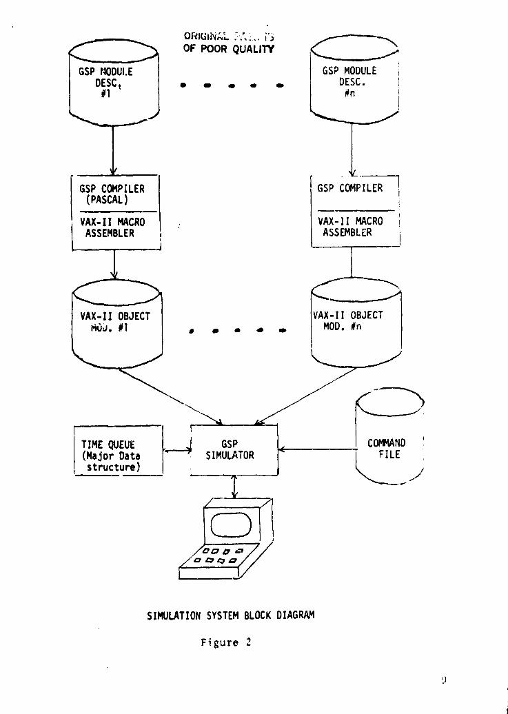
Symbolic level debugging commands were added to examine reg-isters and pins by their source language level names, andset breakpoints on register or pin transitions, sourcestatement line numbers, and subroutine entry and exit. Thesecommands were implemented in such a way that they do nothinder the speed of the simulator when they are not beingused, i.e. the simulator will run in two modes: a slower'debug' mode, and the fast 'production' ( fault experiment,system design validation, etc.) mode. Commands were also beadded to provide a concise yet useful execution traceoutput. A detailed specification for the new language isgiven in is given in the "User's Guide to GSP II", a copyof which has been transmitted along with this report. Ablock diagram of the new simulation system design is shownbelow. The GSP simulator block is written in VAX-11 assem-bler, assembled once, and linked into an executable imagewith the object modules for all modules in a system.
At the time of the writng of this report, the programming ofGSP II is 70 % complete. It is expected that initial use ofthe system will begin this fall. This version of GSP should
8
i
fs
iii
ii
i
OF POOR QUALITY
GSP MODULEDESCt#1
GSP COMPILER(PASCAL)
VAX-II MACROIASSEMBLER
VAX-II OBJECT
I
r+'
TIME QUEUE GSP(Major Data SIMULATORstructure)
CD0 o v d--P
o4Qo/
GSP MODULEDESC.#n
GSP COMPILER l
VAX-1I MACROASSEMBLER i
VAX-II OBJECTMOD. #n
T COMMANDFILE
SIMULATION SYSTEM BLOCK DIAGRAM
Figure 2
Ibe of great value to the modeling and simulation activitiesassociated with AIRLAB.
I A PARALLEL ARCHITECTURE FOR FUNCTIONAL SIMULATION
The functional simulation process has two attributes whichmake it a suitable candidate for parallel processing. Firstthe fact that LSI devices are represented by individual pro-cedures gives a natural partitioning to the process. Second-ly, a logic simulation process, once initiated, requires noinput/output and thus should not be bandwidth limited by I/Orates as was ILI.IAC [10]. A major problem that must besolved, however is.how to solve the contention problem asso-ciated with aecesss to the common time queue by the moduleproceedures and the accompanying synchronization require-ments. A possible approacr to the solution of thesi problemsis outlined below.
' To date, two announced approaches to parallel logic simu-lation have come from IBM and Bell Laboratories. IBM's "sim-ulation engine" uses an array processing approach to performgate level simulation in parallel [8]. It can perform eitherzero or unit de'_dy simulation. The Bell Lab's proposal (incontrast to IBM's mechanization it has never been built),envolves the use of a pipelined organization to exploit par-allelism [9]. It can potentially perform both gate level andfunctional level simulation. They propose that each stage ofthe piprline use high speed logic and be micro-coded inorder to decrease stage de lay. The disadvantage of the pipe-line approach is that the theoretical speed up is limitedby the number of stages that process can be broken downinto i.e. 5 or 6 in the case of logic simulation. Opera-tional speed is of course reduced also by having very faststages.
In contrast to the above, we have begun development of anapproach that would employ a Multiple Instruction MultipleData Stream (MIMD) architecture to peform functional logicsimulation in parallel. We are attempting to exploit t,rosources of potential parallelism in the functional simu-lation process. First, within the simulation of a givensystem, be it "good" or "faulty", one can attempt to executethe proceedures representing the LSI devices in parallel. Asecond and perhaps greater source of parallelism is in theconcurrent execution of N different systems, each having adifferent fault injected.
We have approached the problem by first developing a theore-tical, process level model of the &ystem. Next performanceevaluation techniques have been applied to determine thetheoretical through-put of the proposed system.
10
I
I
t
One the major problems with any parallel. approach to simu-lation is the manner in which the time queue entries arehandled. We have spent some time considering severalapproaches to this problem and we describe one promisingapproach here.
In functional simulation, the internal micro-operations andsignal timing of the device are simulated. This simulationcan be performed using activity orients.', event oriented, orprocess oriented time advancement mec'nanisme [7]. Processoriented simulation seems to offer the most promise of thethree methods since it allows the designer to model eachcomponent module in isolation.The events internal to eachmodule are kept isolated from the events occuring in othermodules.
During the simulation, a time queue is associated with eachmodule, containing the events t,Aat are '-o be executed by themodule in tis,a sequence.A master queue -ontains the inter-module communication events also in ti ►ae order. A represen-tation of these queues is shown in fig. ^.
The events to bwhich representevents occuringarbitrary order,ship as long asrepresented.
e execute3 ina completein differentirrespectivethe order o
a module are grouped in tasksactivity of the module. Themodules are simulated in an
of the actual timing relat• on-f interface events is properly
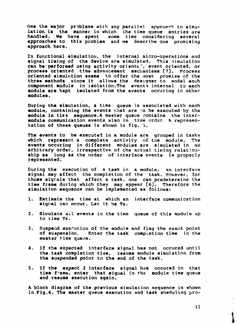
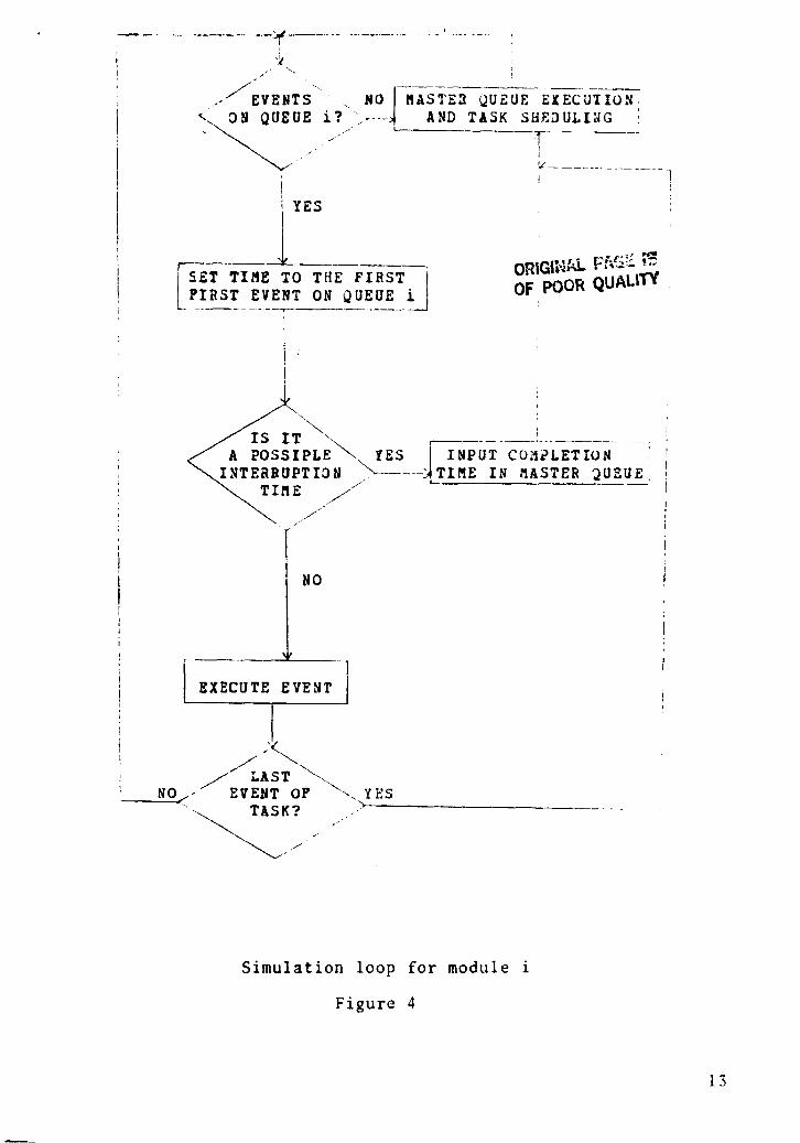
During the executon of a task in a module, an interfacesignal may affect the completion of the task. However, forthose signals that affect a task, one can predetermine thetime frame during which they may appear [ 6]. Therefore thesimulation sequence can be implemented as follows:
1. Estimate the time at which an interface communicationsigi %al can occur. Let it be Ta.
2. Simulate all events in the time queue of this module upto time Ta.
3. Suspend execution of the module and flag the exact pointof suspension. Enter the task completion time in themaster time queue.
4. If the expected interface signal has not occured untilthe task completion time, resume module simulation fromthe suspended point to the end of the task.
S. If the expect .l interface signal has occured in thattime fame, enter that signal in the module time queueand resume execution again.
A block diagram of the previous simulation sequence is shownin Fig . 4. The master queue execution and task sheduling pro-
11
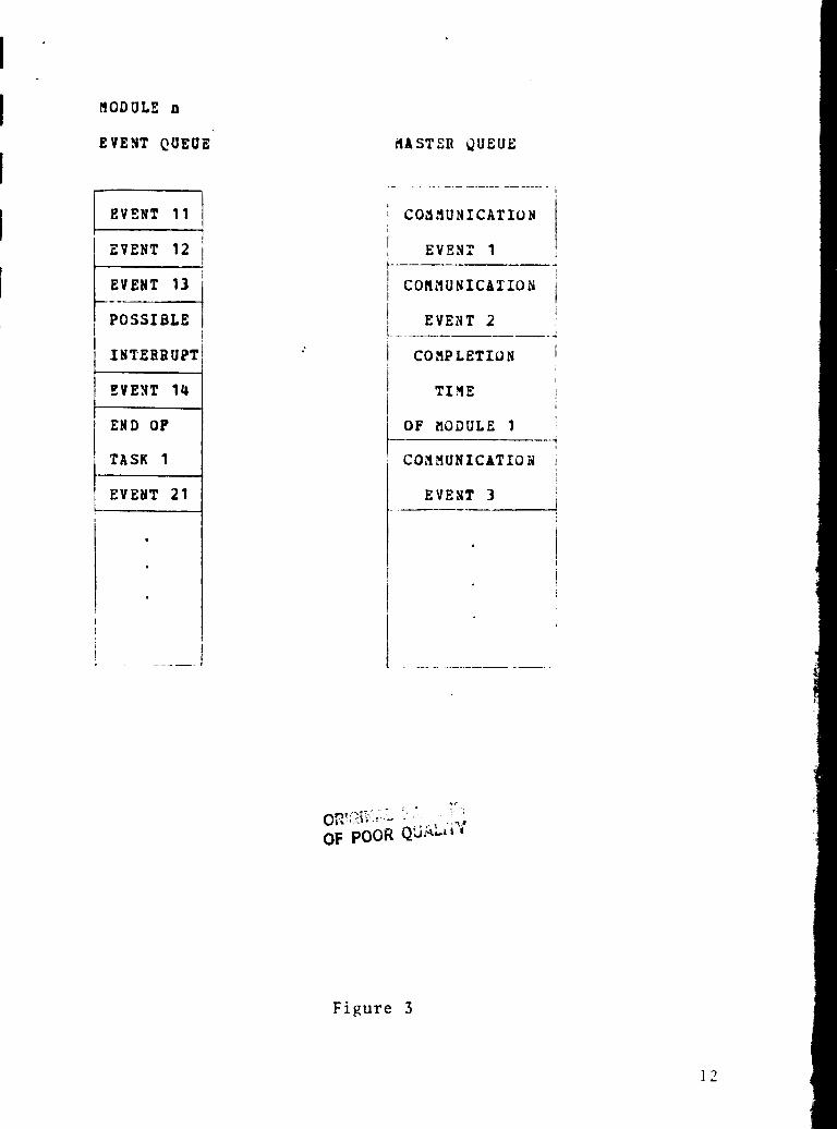
EVENT 11
EVENT 12
EVENT 13
POSSIBLEi
INTEBRUPT^l
EVENT 14
END OF
TASK 1
EVENT 21
+ COMMUNICATION
I
r
EVENT 1
i COHMUNICAIION
EVENT 2i
COMPLETION
i TI"!E
OF MODULE 1
COMMUNICATION i
EVENT 3
12
MODULE n
EVENT QUEUE
7AST"-R QUEUE
13
i •1
`EVENTS NO] MASTE3 QUEUE EXECUTIUN' ON QUEUE i? - - AND TASK SHEBULING
YES
SET TIhE TO THE FIRST0RIGRAIIA.
FIRST EVENT ON QUEUE i,OF FOR QUALITY
i
1
IS ITA POSSIPLE YES
INTERRUPTIONTIME
1 NO
II
EXECUTE EVENT.
i
LASTN0,- /EVENT OF ^^, Y E S
TASK?
f
R
f
INPUT COMPLETIUNTIME IN MASTER 2U--UE
iiiI
i
i
Simulation loop for module i
Figure 4

Igram keeps track of the interface signals and propagates
' them to the corresponding modules. It also initiates taskexecution simulation sequences for the modules.
' The proposed simulation scheme has the advantage of reducingalternate module execution at each time step, since only theintermodule communication signals affect the event execution
' at each module.
The details of this work are contained in a separate report:"A Parallel Approach to Functional, Process Oriented Simu-lation" which is in preparation at his time. A copy will beforwarded to NASA when it is completed.
t
t
t14
t
and V.
15
IPUBLICATIONS
During the performance period the following publicationswere prepared. The papers listed below were either pre-sented at conferences or submitted to appropriate journals.
PAPERS
1. "GSP:J.R. Armstrong and D.E. Devlin,A Logic Simulatorfor LSI", Proceedings of the Eighteenth Design Auto-mation Conference, pp 518-524.
2. V. Puthenpurayil and J.R. Armstrong, "Functional LevelModeling of LSI Devices", Proceedings of the FourteenthSoutheastern Symposium on System Theory, pp 290-293.
3. S.Sathe,J.R. Armstrong, and F.G. Gray, "Functional LevelFault Simulation Techniques", Proceedings of the Four-teenth Southeastern Symposium on System Theory, pp285-290.
4. J.R. Armstrong, "Chip Level Modeling and Simulation",accepted for publication in Simulation, October 1983issue.
5. "Chip ",J. R. Armstrong, Level Modeling of LSI Devicessubmitted for publication in the "IEEE Transactions onComputer Aided Design of Integrated Circuits"
6. J.R. Armstrong and F.G.Gray, "Fault Diagnosis in a Boo-lean n Cube Array of Microprocessors", IEEE Transactionson Computers; vol. c-30, no. 8,Aug. 1981, pp 587-590.
I THESES AND REPORTS
1. V.Puthenpurayil, "Functional Level Modeling of DigitalDevices", Masters Thesis,Department of Electrical Engi-neering, Va. Tech., Sept. 1982.
2. Shirish Sathe, "Functional Level Fault Simulation in LSIDevices." Masters Thesis, Department of ElectricalEngineering, Va. Tech., June 1982.
3. J.R. Armstrong, "Chip Level Modeling Techniques", Tech-nical Report 8124, EE Dept, Va. Tech, Nov. 1981.
4. D. Levlin,J. R. Armstrong,S. Sathe,Puthenpurayil,"GSP Users Guide", Sept. 1982.
t
5. V. Puthenpurayil, "Modeling the BDX930", TechnicalReport, EE Dept, Va. Tech, June 1982.
6. J. R. Armstrong and F. G. Gray, "Status Report forNAG-1-174: Chip Level Simulation of Fault Tolerant Com-puters,Performance Period: June 1,1981 Through May31,1982.
7. M. Iacoponi, "User's Guide for VAX Version of GSP andVAX BDX-930 RAM/ROM Loader"
8. J. Kerr, "GSP II User's Guide", EE Dept, Va. Tech., July1983.
I TEXTUAL REFERENCES
1. Armstrong, J.R., Woodruff, G.W., "Chip Level Simulationof Microprocessors", Computer, Vol. 13 ,No. 1, pp.94-100,Jan. 1980.
2. Armstrong, J.R., Devlin D.E., "GSP-A Logic Simulator forLSI", Proceedings of the 18th Annual Design AutomationConference, pp. 518-524, Nashville, Tn, June 1981.
3. Armstrong, J.R., Thierbach, M. and Ellis, M.D., FinalReport for NSWC Contract No N60921-78-A025, Vol. 3:Microprocessor Simulation.
4. Armstrong, J.R. and Gray F.G., "MicroprocessorSelf-Test", Final Report for RADC ContractF30602-80-200.
5. Armstrong, J,R. and Gray F.G.," Chip Level Simulation ofFault Tolerant Computers", Status Report For NASA GrantNAG-1-174, June 1, 1982.
6. Armstrong, J.R., "Chip Level Modeling Techniques", EEDept. Technical Report, May 31,1982.
7. Leinwand, Sany M., "Process Oriented Logic Simulation,Proceedings of the 18th Design Automation Conference.Nashville Tenn., June 1981.
8. "TheFister, G.F., Yorktown SimulationEngine:Introduction" and Denneau, M. M., "The YorktownSimulation Engine", Proceedings of the 19th Design Auto-mation Conference, Las Vegas, Nev., June 1982.
9. M. Abromovici, et. all," A Logic Simulation Machine",Proceedings of the 19th Design Automation Conference,Las Vegas, Nev., June 1982.
16
t