Embed Size (px)
Citation preview
Operating manual
Power Quality Interface
GB PQI-D model
We take care of it.
Page 2
Note:
The current version of the operating manual is based on firmware versions > 4.0.05 (2x4xU)
and > 5.0.11 (4xU, 4xI).
It is updated continuously.
For newer versions, either contact us directly or refer to the most recent version of the op-
erating manual, available on our website (www.a-eberle.de).
A. Eberle GmbH & Co. KG
Frankenstraße 160
90461 Nuremberg, Germany
Telephone: 0911 / 62 81 08 0
Fax: 0911 / 62 81 08 96
E-mail: [email protected]
Internet: www.a-eberle.de
A. Eberle GmbH & Co. KG cannot be held liable for any damage or losses resulting from print-
ing errors or changes to this operating manual.
Furthermore, A. Eberle GmbH & Co. KG does not assume responsibility for any damage or
losses resulting from defective devices or from devices altered by the user.
Copyright 2012 by A. Eberle GmbH & Co. KG.
Subject to change.
Page 3
Contents
1. Safety information ................................................................................................................ 8
1.1 Electrical safety ..................................................................................................................... 8
1.2 Mounting ............................................................................................................................... 9
2. Technical concept ............................................................................................................... 10
2.1 Application .......................................................................................................................... 10
2.2 PQI-D Power Quality Interface features............................................................................... 12
2.3 Description .......................................................................................................................... 13
3. Fault recorder ..................................................................................................................... 14
3.1 Event recorder ..................................................................................................................... 14
3.2 Oscilloscope, r.m.s. value recorder ...................................................................................... 15
3.2.1 Trigger conditions ................................................................................................................ 15
3.2.2 External trigger .................................................................................................................... 16
3.2.3 Fault record: pre-trigger and re-trigger time ....................................................................... 17
3.2.4 Oscilloscope recorder .......................................................................................................... 18
3.2.5 R.m.s. value recorder ........................................................................................................... 19
3.3 Signal voltage recorder ........................................................................................................ 20
3.4 Harmonic recorder .............................................................................................................. 21
4. Technical data ..................................................................................................................... 22
4.1 Regulations and standards .................................................................................................. 22
4.2 Voltage inputs ..................................................................................................................... 23
4.3 Current inputs ..................................................................................................................... 24
4.4 Analogue outputs ................................................................................................................ 25
4.5 Binary inputs........................................................................................................................ 26
4.6 Binary outputs (BO) ............................................................................................................. 26
4.7 Limit value monitoring......................................................................................................... 27
4.8 Overview of measurement quantities ................................................................................. 27
4.8.1 Deduced measurement quantities: ..................................................................................... 28
4.8.2 Statistical quantities: ........................................................................................................... 31
4.8.3 Overview of events: ............................................................................................................. 32
4.8.4 Overview of binary message singals, 4xU and 4xI ................................................................ 39
4.8.5 Device 8 x U ......................................................................................................................... 42
4.9 Reference conditions ........................................................................................................... 49
4.10 Measurement data acquisition ............................................................................................ 49
4.11 Data memory ....................................................................................................................... 49
We take care of it.
Page 4
4.12 Electromagnetic compatibility ............................................................................................ 50
4.13 Electrical safety ................................................................................................................... 51
4.14 Operating voltages .............................................................................................................. 51
4.15 Power supply ....................................................................................................................... 51
4.16 Binary inputs and outputs, analogue outputs ...................................................................... 52
4.17 Environmentalconditions..................................................................................................... 53
5. Mechanical design .............................................................................................................. 54
5.1 Plug-in module .................................................................................................................... 54
5.2 Housing ............................................................................................................................... 54
5.3 Assignment of socket connectors 1 ... 5............................................................................... 58
5.3.1 Socket connector 1 .............................................................................................................. 58
5.3.2 Socket connector 2 .............................................................................................................. 58
5.3.3 Socket connector 3 - feature C20 ... C31 .............................................................................. 62
5.3.4 Socket connector 4 .............................................................................................................. 62
5.3.5 Socket connector, 5 interfaces ............................................................................................ 69
5.4 Block diagrams .................................................................................................................... 71
5.4.1 Block diagram feature C10 / M00, M96 ............................................................................... 71
5.4.2 Block diagram feature C20...C31 / M92 ............................................................................... 71
5.4.3 Block diagram feature C20...C31 / M93 ............................................................................... 72
5.4.4 Block diagram feature C20...C31 / M94 .............................................................................. 72
5.4.5 Block diagram feature C20...C31 / M95 ............................................................................... 72
5.4.6 Block diagram feature C40...C41, M97, M98 ....................................................................... 73
6. Serial interfaces .................................................................................................................. 73
6.1 RS232 interfaces .................................................................................................................. 74
6.2 RS485 interfaces .................................................................................................................. 74
6.3 E-LAN (Energy - Local Area Network) ................................................................................... 74
6.3.1 Features............................................................................................................................... 74
6.3.2 Operation ............................................................................................................................ 75
6.4 COM3 .................................................................................................................................. 77
6.5 Time and trigger bus ............................................................................................................ 78
6.6 Time synchronisation........................................................................................................... 78
6.6.1 RS232 interface of the time master (COM): ......................................................................... 78
6.6.2 Time synchronisation bus (RS485): ...................................................................................... 78
6.7 External trigger .................................................................................................................... 80
7. Voltage quality monitor ...................................................................................................... 81
7.1 Standard analysis ................................................................................................................. 81
Page 5
7.1.1 Overview EN50160 (2010) ................................................................................................... 82
7.1.2 Characteristics of the voltage supply ................................................................................... 83
7.2 Network quality events ....................................................................................................... 87
7.2.1 Interval events ..................................................................................................................... 88
7.2.2 Start / stop events ............................................................................................................... 89
7.2.3 Prioritising events ................................................................................................................ 90
7.3 Flagging ............................................................................................................................... 91
7.3.1 Binary event notification signals .......................................................................................... 91
7.3.2 Aggregation of statistical values .......................................................................................... 92
7.3.3 Monitoring statistical values ................................................................................................ 92
7.3.4 Controlling the event evaluation ......................................................................................... 93
7.4 Basic setting for PQI-D ......................................................................................................... 93
8. Measurement circuits ......................................................................................................... 94
8.1 Connection possibilities ....................................................................................................... 94
8.2 Current transformer connections ........................................................................................ 95
8.2.1 PQI-D current transformer connection ................................................................................ 96
8.3 Voltage transformer connections ........................................................................................ 97
8.3.1 Voltage transformer connection PQI-D................................................................................ 98
8.4 Reference voltage ................................................................................................................ 99
8.5 Network frequency .............................................................................................................. 99
8.6 System time ......................................................................................................................... 99
8.7 Binary inputs...................................................................................................................... 100
8.8 Binary outputs ................................................................................................................... 100
8.9 Analogue outputs .............................................................................................................. 100
8.10 Analogue inputs ................................................................................................................. 101
8.11 LED display ........................................................................................................................ 101
8.12 Synchronisation of interval average power values ............................................................ 101
9. Data management ............................................................................................................ 102
9.1 Measurement data classes ................................................................................................ 102
9.2 Memory configuration ....................................................................................................... 103
10. Definition of the measurement quantities ....................................................................... 105
10.1 Sampling values ................................................................................................................. 105
10.2 Half-period values ............................................................................................................. 105
10.2.1 R.m.s. values ...................................................................................................................... 106
10.2.2 Synchronised sampling values ........................................................................................... 106
10.2.3 10/12-period values .......................................................................................................... 107
We take care of it.
Page 6
10.2.4 150/180-period values....................................................................................................... 107
10.2.5 10-minute values ............................................................................................................... 108
10.2.6 2-hour values ..................................................................................................................... 108
10.3 Sampling values ................................................................................................................. 109
10.3.1 Primary sampling values .................................................................................................... 109
10.3.2 Phase-to-phase sampling values ........................................................................................ 109
10.4 R.m.s. voltage values ......................................................................................................... 110
10.5 Negative deviation, positive deviation............................................................................... 111
10.6 R.m.s. current values ......................................................................................................... 111
10.7 Network frequency ............................................................................................................ 111
10.8 Spectral analysis ................................................................................................................ 111
10.8.1 R.m.s. values of the harmonic subgroups .......................................................................... 111
10.8.2 R.m.s. values of the interharmonic subgroups................................................................... 112
10.8.3 Harmonic distortions ......................................................................................................... 112
10.8.4 Signal voltage .................................................................................................................... 114
10.8.5 Phase of the voltages, currents to reference voltage (fundamental oscillation) ................ 114
10.8.6 Phase of the phase voltages to associated conductor currents (fundamental oscillation) . 114
10.8.7 Phase of the current harmonics to the phase voltage fundamental oscillation ................. 114
10.9 Symmetrical components, asymmetries, phase sequence ................................................ 115
10.10 Power measurement quantities ........................................................................................ 117
10.10.1 Active powers .................................................................................................................... 117
10.10.2 Apparent power ................................................................................................................ 119
10.10.3 Reactive power .................................................................................................................. 121
10.10.4 Dimensionless power measurement quantities ................................................................. 123
10.10.5 Active energies .................................................................................................................. 126
10.10.6 Reactive energies .............................................................................................................. 126
10.11 Flicker magnitude .............................................................................................................. 127
11. Transnostic ........................................................................................................................ 128
12. Updating the firmware ..................................................................................................... 129
13. Maintenance and current consumption ........................................................................... 131
13.1 Changing the fuse .............................................................................................................. 131
13.2 Changing the battery ......................................................................................................... 131
13.3 PQI-D current consumption ............................................................................................... 132
14. Scope of delivery............................................................................................................... 133
15. Storage information .......................................................................................................... 133
16. Guarantee ......................................................................................................................... 133
Page 7
17. Ordering information ........................................................................................................ 134
We take care of it.
Page 8
Safety information
Electrical safety
Before you begin to commission the device, you should be aware of some of the dangers
that may occur if the device is used improperly.
1 The PQI-D is a device with degree of protection I. Before it is connected to the voltage, it
must first be connected to the system's earthing system via its protective earth connection.
1 The connected circuits must not exceed the protection category of the device
(e.g. measurement inputs: CAT III / 300 V).
1 The device must not be used in circuits that contain corona discharges.
1 The device must be removed from the network immediately if it is determined that the
device can no longer be operated safely due to a mechanical or electrical fault.
1 Please note: if the Power Quality Interface is installed in a housing, the secondary circuits
of the current transformer must be short-circuited before the terminal connections of the
current transformers are removed from the device. Devices in 19” enclosures are protected
against short circuits via a device built in to the terminal block. The modules can be plugged
in and withdrawn at will, without having to short-circuit the current transformer(s) first.
1 Please note that there is a danger to life wherever a voltage of > 50 V r.m.s. is present.
Page 9
Mounting
The operational safety of the device can only be ensured when the electrical connec-
tion data of the device supplied match the requirements which apply at the installation
location.
.
Please check the following parameters against the type plate:
1 Auxiliary voltage input: Supply voltage range
AC nominal range 100V ... 240V -
AC operating range 90 ... 264 V
DC nominal range 100 ... 300 V 20 ... 70 V
DC operating range 100 ... 300 V 18 ... 72 V
1 Current measurement inputs: max. continuous current/input voltage
C20; C21 : 5A
C30, C31 : 10A
C40, C41 : 230 mV RMS
1 Voltage measurement inputs: max. conductor-to-earth voltage
E1 : 200 V AC
E2 : 460 V AC
E9 : 200 V AC, 460 V AC
1 Binary inputs: Maximum input voltage
Mxx.0 : 48…250 V AC/DC
Mxx.1 : 10…48 V DC
We take care of it.
Page 10
Technical concept
Application
The state-of-the-art PQI-D power quality interface for medium and high voltage networks is
the central component of a system for carrying out all of the required measurement tasks in
electrical networks. The PQI-D can be used as both a power quality interface compliant with
DIN EN 50160 and as a measurement device for measuring all physically-defined measure-
ment quantities in AC electrical networks.
The component is primarily designed to monitor special reference quantities and quality
agreements between the energy supplier and the customer, as well as to record, analyse and
save the data.
Modern voltage quality measurement devices operate according to the IEC 61000-4-30
standard. This standard defines measurement methods and so provides the user with a basis
for comparison. Devices from different manufacturers which function in accordance with this
standard must provide the same measurement results.
The standard defines two measuring device classes.
Class A measuring devices are used primarily for measurements related to contracts in the
customer/supplier relationship, while Class B measuring devices can be used for determining
statistical quality values.
The PQI-D complies with the requirements of IEC 610004- 30 (2008) for class A devices for all
parameters.
1 Parameter Class
0 Accuracy of voltage measurement A
0 Determination of time intervals A
0 Marking of measurement values for events A
0 Harmonics, interharmonics A
0 Flicker A
0 Frequency A
0 Voltage asymmetry A
0 Recording of events A
0 Synchronisation A
Five procedures are available for event-triggered fault recording:
The event recorder stores the messages that denote the type, time and properties of
events in chronological order.
The oscilloscope recorder stores the sampling values of fault events with pre-event and
post-event history.
Page 11
The r.m.s. recorder stores the half-period r.m.s. values of fault events with pre-event and
post-event history.
The signal voltage recorder stores the 10/12-period r.m.s. values of an adjustable frequency
range (e.g. ripple-control frequency).
The harmonic recorder stores the 10-minute spectrum of the harmonics from the 2nd to
50th harmonic for voltages and currents.
All fault records are triggered by an event or combination of events which can be freely de-
fined. This enables phase-phase and phase-earth events to be recorded simultaneously.
Event messages (e.g. limit value violations) can also be signalled directly via relays if required.
The device has two RS232 interfaces (COM 1 and COM 2) and two E-LAN (Energy Local Area
Network) system/transport bus interfaces, which can be used to network up to 255 REGSys™
devices (e.g. REG-D / EOR-D).
WinPQ and WinPQ Para Express are available as PC programs.
It supports the parameterisation, download and time-constant backup of measurement data
in a database on the PC.
The measurement data can be accessed continuously, cyclically or once only by the device.
Both offline data (from the database) and online data (from the device) can be displayed.
A button protected against unintentional touching is provided for firmware updates.
The device is available in several different versions.
Current inputs are available for the measurement circuit (C20, C30) and for the protective
circuit (C21, C31).
The following input configurations can be selected:
0 4 voltage transformers for conventional power quality applications (feature C00)
0 8 voltage transformers for power quality applications in double busbar systems (feature
C10)
0 4 voltage transformers and 4 current transformers for power quality and general meas-
urement tasks.
If the PQI-D is supplied in a 20TE or 30TE housing, the desired number and type of inputs and
outputs on the terminal strip must be specified.
The version should be specified since the plug-in module offers a wide range of different
inputs and outputs, but the options for connecting terminals are limited.
We take care of it.
Page 12
PQI-D Power Quality Interface features
0 Measuring the voltage quality according to DIN EN 50160
0 Class A device according to IEC 61000- 4-30
0 10.24 kHz sampling frequency
0 Fault recorder function up to 20 · nominal current (100 x In)
0 Phase-phase and phase-earth measurements are possible simultaneously
0 Voltage measurement channels for U12, U23, U31, UNE
0 Additional measurement of currents I1, I2, I3, I0
0 Determination of over 3000 measurement values
0 Freely programmable limit values and outputs using isolated contacts
0 Five freely programmable LEDs
0 Freely programmable binary inputs to start and stop measurements remotely
0 Adoption of conventional measurement transducer functions; up to eight measure-
ment quantities can be chosen and output via an mA signal.
0 Analysis of the data via a mySQL-supported database with the help of the WinPQ soft-
ware package
0 Connection to the control system according to IEC 870-5-103
0 Connection to the control system according to IEC 61850
Page 13
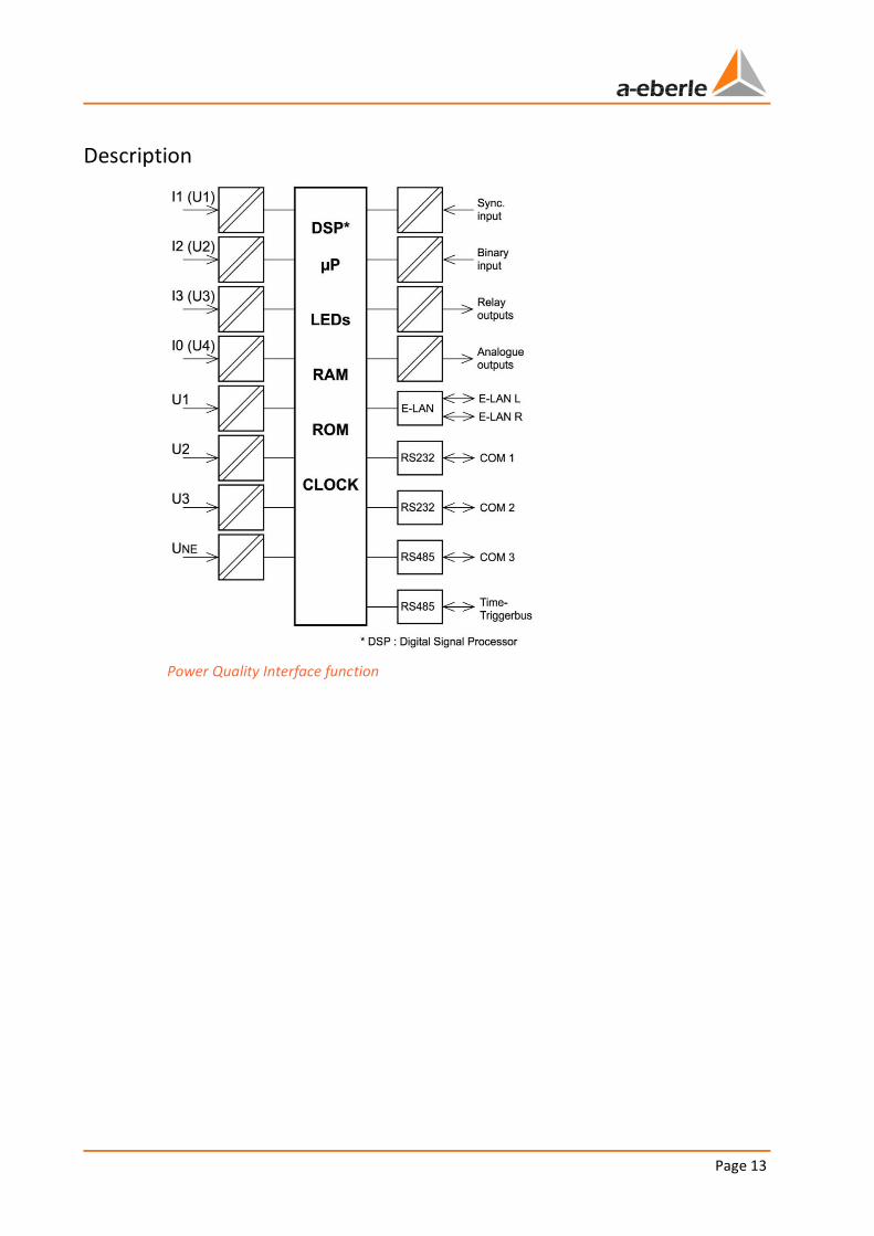
Description
Power Quality Interface function
We take care of it.
Page 14
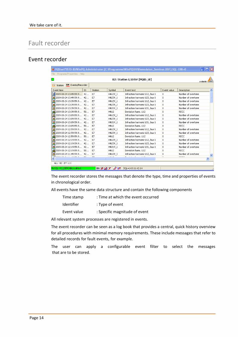
Fault recorder
Event recorder
The event recorder stores the messages that denote the type, time and properties of events
in chronological order.
All events have the same data structure and contain the following components
Time stamp : Time at which the event occurred
Identifier : Type of event
Event value : Specific magnitude of event
All relevant system processes are registered in events.
The event recorder can be seen as a log book that provides a central, quick history overview
for all procedures with minimal memory requirements. These include messages that refer to
detailed records for fault events, for example.
The user can apply a configurable event filter to select the messages
that are to be stored.
Page 15
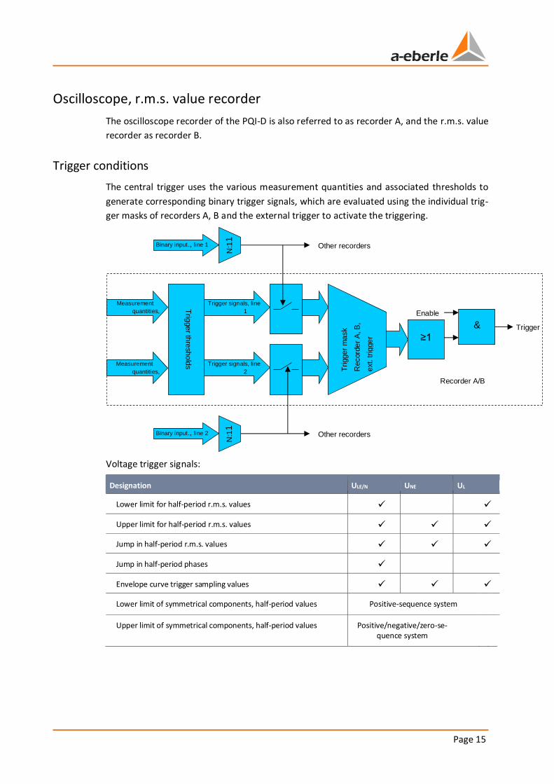
Oscilloscope, r.m.s. value recorder
The oscilloscope recorder of the PQI-D is also referred to as recorder A, and the r.m.s. value
recorder as recorder B.
Trigger conditions
The central trigger uses the various measurement quantities and associated thresholds to
generate corresponding binary trigger signals, which are evaluated using the individual trig-
ger masks of recorders A, B and the external trigger to activate the triggering.
Voltage trigger signals:
Designation ULE/N UNE UL
Lower limit for half-period r.m.s. values
Upper limit for half-period r.m.s. values
Jump in half-period r.m.s. values
Jump in half-period phases
Envelope curve trigger sampling values
Lower limit of symmetrical components, half-period values Positive-sequence system
Upper limit of symmetrical components, half-period values Positive/negative/zero-se-quence system
N:1
1
Binary input., line 1
Trigger signals, line
1
Tri
gge
r m
ask
Record
er
A, B
,
ext. tri
gge
r
Trigger signals, line
2
≥1
& Trigger
Enable
Other recorders
Trig
ge
r thre
sh
old
s
Measurement
quantities,
line 1
Measurement
quantities,
line 2 Recorder A/B
N:1
1
Binary input., line 2 Other recorders
We take care of it.
Page 16
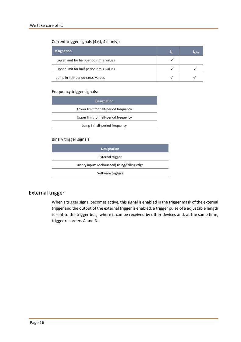
Current trigger signals (4xU, 4xI only):
Designation IL IE/N
Lower limit for half-period r.m.s. values
Upper limit for half-period r.m.s. values
Jump in half-period r.m.s. values
Frequency trigger signals:
Designation
Lower limit for half-period frequency
Upper limit for half-period frequency
Jump in half-period frequency
Binary trigger signals:
Designation
External trigger
Binary inputs (debounced) rising/falling edge
Software triggers
External trigger
When a trigger signal becomes active, this signal is enabled in the trigger mask of the external
trigger and the output of the external trigger is enabled, a trigger pulse of a adjustable length
is sent to the trigger bus, where it can be received by other devices and, at the same time,
trigger recorders A and B.
Page 17
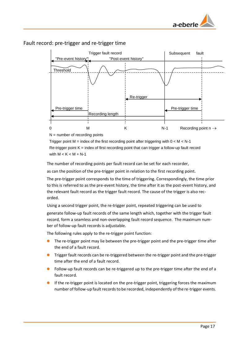
Fault record: pre-trigger and re-trigger time
The number of recording points per fault record can be set for each recorder,
as can the position of the pre-trigger point in relation to the first recording point.
The pre-trigger point corresponds to the time of triggering. Correspondingly, the time prior
to this is referred to as the pre-event history, the time after it as the post-event history, and
the relevant fault record as the trigger fault record. The cause of the trigger is also rec-
orded.
Using a second trigger point, the re-trigger point, repeated triggering can be used to
generate follow-up fault records of the same length which, together with the trigger fault
record, form a seamless and non-overlapping fault record sequence. The maximum num-
ber of follow-up fault records is adjustable.
The following rules apply to the re-trigger point function:
0 The re-trigger point may lie between the pre-trigger point and the pre-trigger time after
the end of a fault record.
0 Trigger fault records can be re-triggered between the re-trigger point and the pre-trigger
time after the end of a fault record.
0 Follow-up fault records can be re-triggered up to the pre-trigger time after the end of a
fault record.
0 If the re-trigger point is located on the pre-trigger point, triggering forces the maximum
number of follow-up fault records to be recorded, independently of the re-trigger events.
"Pre-event history" "Post-event history"
Recording length Pre-trigger time
Re-trigger
window
0 M K N-1 Recording point n
N = number of recording points
Trigger point M = index of the first recording point after triggering with 0 < M < N-1
Re-trigger point K = index of first recording point that can trigger a follow-up fault record
with M < K < M + N-1
Threshold
Pre-trigger time
Trigger fault record Subsequent fault
record
We take care of it.
Page 18
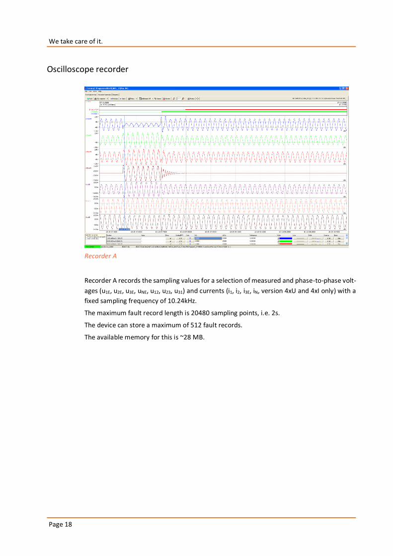
Oscilloscope recorder
Recorder A
Recorder A records the sampling values for a selection of measured and phase-to-phase volt-
ages (u1E, u2E, u3E, uNE, u12, u23, u31) and currents (i1, i2, i3E, iN, version 4xU and 4xI only) with a
fixed sampling frequency of 10.24kHz.
The maximum fault record length is 20480 sampling points, i.e. 2s.
The device can store a maximum of 512 fault records.
The available memory for this is ~28 MB.
Page 19
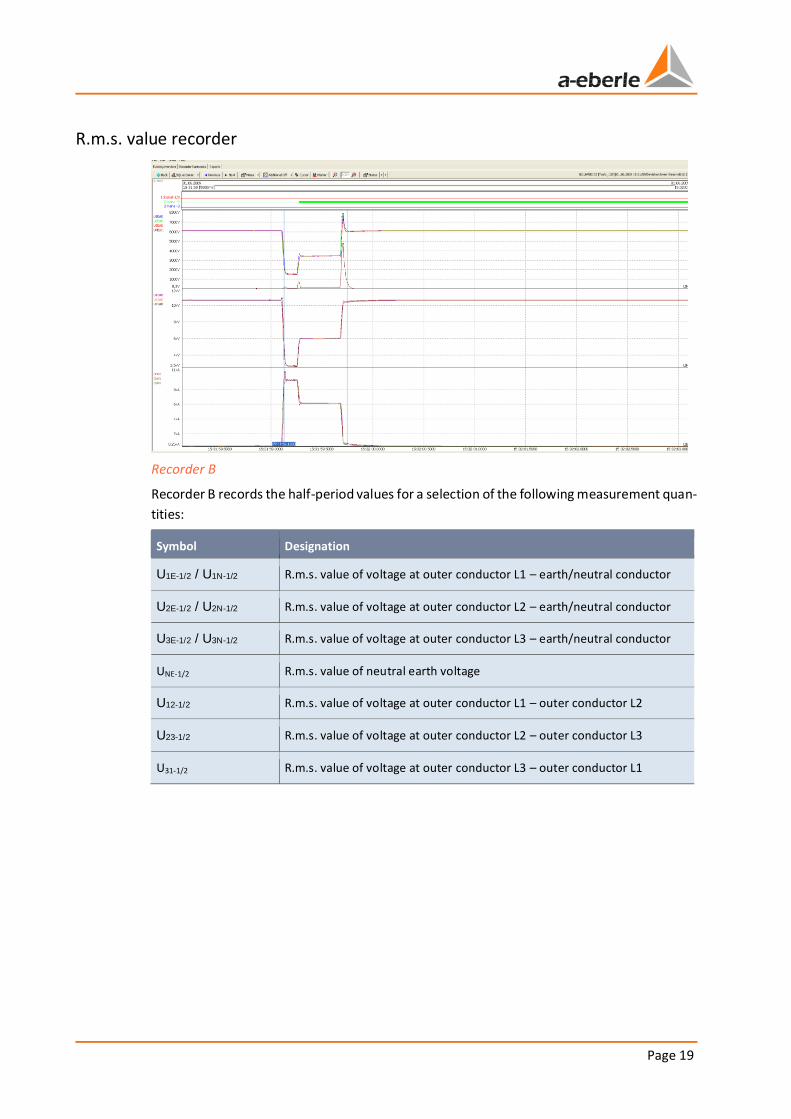
R.m.s. value recorder
Recorder B
Recorder B records the half-period values for a selection of the following measurement quan-
tities:
Symbol Designation
U1E-1/2 / U1N-1/2 R.m.s. value of voltage at outer conductor L1 – earth/neutral conductor
U2E-1/2 / U2N-1/2 R.m.s. value of voltage at outer conductor L2 – earth/neutral conductor
U3E-1/2 / U3N-1/2 R.m.s. value of voltage at outer conductor L3 – earth/neutral conductor
UNE-1/2 R.m.s. value of neutral earth voltage
U12-1/2 R.m.s. value of voltage at outer conductor L1 – outer conductor L2
U23-1/2 R.m.s. value of voltage at outer conductor L2 – outer conductor L3
U31-1/2 R.m.s. value of voltage at outer conductor L3 – outer conductor L1
We take care of it.
Page 20
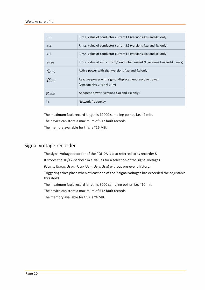
I1-1/2 R.m.s. value of conductor current L1 (versions 4xu and 4xI only)
I2-1/2 R.m.s. value of conductor current L2 (versions 4xu and 4xI only)
I3-1/2 R.m.s. value of conductor current L3 (versions 4xu and 4xI only)
IE/N-1/2 R.m.s. value of sum current/conductor current N (versions 4xu and 4xI only)
P(1/2) Active power with sign (versions 4xu and 4xI only)
Q(1/2) Reactive power with sign of displacement reactive power
(versions 4xu and 4xI only)
S(1/2) Apparent power (versions 4xu and 4xI only)
f1/2 Network frequency
The maximum fault record length is 12000 sampling points, i.e. ~2 min.
The device can store a maximum of 512 fault records.
The memory available for this is ~16 MB.
Signal voltage recorder
The signal voltage recorder of the PQI-DA is also referred to as recorder S.
It stores the 10/12-period r.m.s. values for a selection of the signal voltages
(Us1E/N, Us2E/N, Us3E/N, UsNE, Us12, Us23, Us31) without pre-event history.
Triggering takes place when at least one of the 7 signal voltages has exceeded the adjustable
threshold.
The maximum fault record length is 3000 sampling points, i.e. ~10min.
The device can store a maximum of 512 fault records.
The memory available for this is ~4 MB.
Page 21
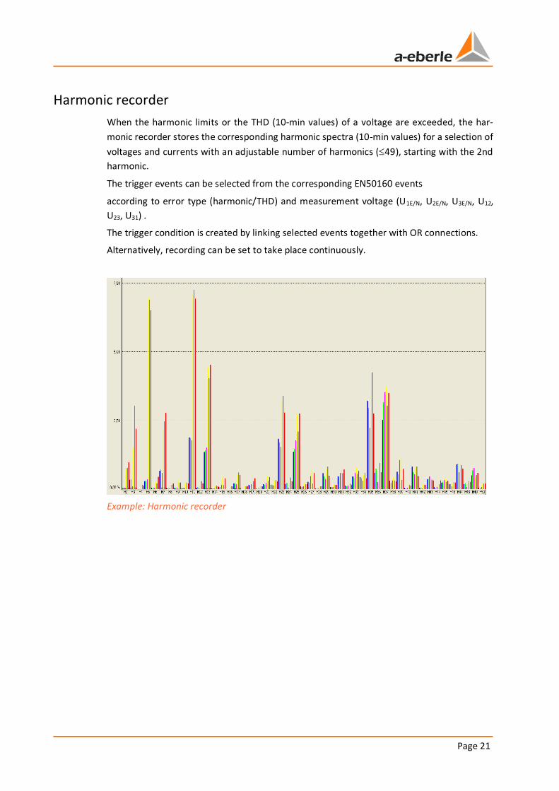
Harmonic recorder
When the harmonic limits or the THD (10-min values) of a voltage are exceeded, the har-
monic recorder stores the corresponding harmonic spectra (10-min values) for a selection of
voltages and currents with an adjustable number of harmonics (49), starting with the 2nd
harmonic.
The trigger events can be selected from the corresponding EN50160 events
according to error type (harmonic/THD) and measurement voltage (U1E/N, U2E/N, U3E/N, U12,
U23, U31) .
The trigger condition is created by linking selected events together with OR connections.
Alternatively, recording can be set to take place continuously.
Example: Harmonic recorder
We take care of it.
Page 22
Technical data
Regulations and standards
IEC 61010-1 / DIN EN 61010-1
IEC 60255-4 / DIN EN 60255-4
IEC 61326-1 / DIN EN 61326-1
IEC 60529 / DIN EN 60529
IEC 60068-1 / DIN EN 60068-1
IEC 60688 / DIN EN 60688
IEC 61000-6-2 / DIN EN 61000-6-2
IEC 61000-6-4 / DIN EN 61000-6-4
IEC 61000-6-5 / DIN EN 61000-6-5
IEC 61000-4-30 / DIN EN 61000-4-30
IEC 61000-4-7 / DIN EN 61000-4-7
IEC 61000-4-15 / DIN EN 61000-4-15
IEC 61000-3-3 / DIN EN 61000-3-3
DIN EN 50160
Page 23
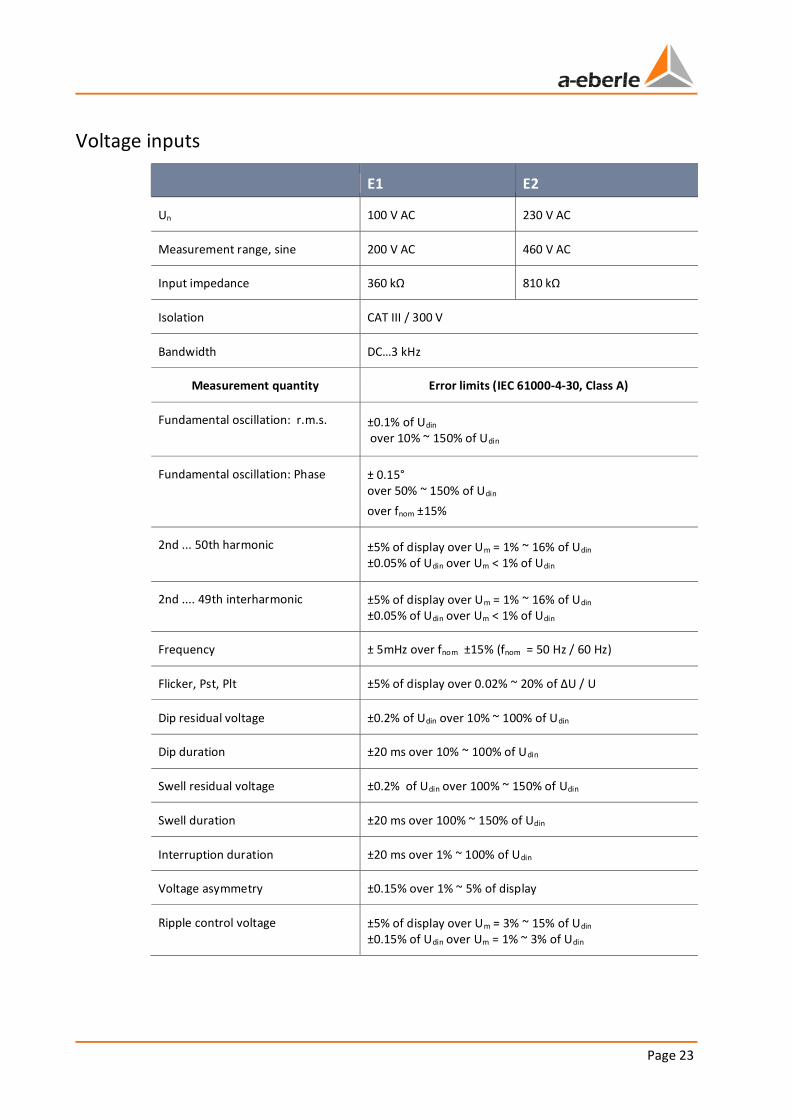
Voltage inputs
E1 E2
Un 100 V AC 230 V AC
Measurement range, sine 200 V AC 460 V AC
Input impedance 360 kΩ 810 kΩ
Isolation CAT III / 300 V
Bandwidth DC…3 kHz
Measurement quantity Error limits (IEC 61000-4-30, Class A)
Fundamental oscillation: r.m.s.
±0.1% of Udin over 10% ~ 150% of Udin
Fundamental oscillation: Phase
± 0.15° over 50% ~ 150% of Udin
over fnom ±15%
2nd ... 50th harmonic
±5% of display over Um = 1% ~ 16% of Udin ±0.05% of Udin over Um < 1% of Udin
2nd .... 49th interharmonic ±5% of display over Um = 1% ~ 16% of Udin ±0.05% of Udin over Um < 1% of Udin
Frequency ± 5mHz over fnom ±15% (fnom = 50 Hz / 60 Hz)
Flicker, Pst, Plt ±5% of display over 0.02% ~ 20% of ∆U / U
Dip residual voltage ±0.2% of Udin over 10% ~ 100% of Udin
Dip duration ±20 ms over 10% ~ 100% of Udin
Swell residual voltage ±0.2% of Udin over 100% ~ 150% of Udin
Swell duration ±20 ms over 100% ~ 150% of Udin
Interruption duration ±20 ms over 1% ~ 100% of Udin
Voltage asymmetry ±0.15% over 1% ~ 5% of display
Ripple control voltage ±5% of display over Um = 3% ~ 15% of Udin ±0.15% of Udin over Um = 1% ~ 3% of Udin
We take care of it.
Page 24
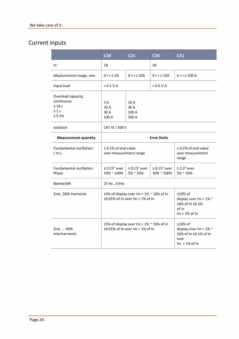
Current inputs
C20 C21 C30 C31
In 1A 5A
Measurement range, sine 0 < I ≤ 2A 0 < I ≤ 20A 0 < I ≤ 10A 0 < I ≤ 100 A
Input load < 0.1 V A < 0.5 V A
Overload capacity, continuous
≤ 10 s ≤ 1 s ≤ 5 ms
5 A 10 A 30 A 100 A
10 A 30 A 100 A 500 A
Isolation CAT III / 300 V
Measurement quantity Error limits
Fundamental oscillation: r.m.s.
± 0.1% of end value over measurement range
± 0.2% of end value over measurement range
Fundamental oscillation: Phase
± 0.15° over 10% ~ 100%
± 0.15° over 5% ~ 50%
± 0.15° over 10% ~ 100%
± 1.0° over 5% ~ 10%
Bandwidth 25 Hz…3 kHz
2nd...50th harmonic
±5% of display over Im = 1% ~ 16% of In ±0.05% of In over Im < 1% of In
±10% of
display over Im = 1% ~
16% of In ±0.1% of In Im < 1% of In
2nd .... 49th interharmonic
±5% of display over Im = 1% ~ 16% of In ±0.05% of In over Im < 1% of In
±10% of display over Im = 1% ~ 16% of In ±0.1% of In over Im < 1% of In
Page 25
Feature C40: mV inputs for Rogowski coils
Input resistance 10 kΩ
Full scale range 150 mV
Note:
In order to guarantee measurement accuracy, only Rogowski coils from A. Eberle GmbH &
Co. KG should be used.
Feature C41: mV inputs for mini clamps
Input resistance 2 M Ω
Full scale range 230 mV
Analogue outputs
Refer to ordering information for number
Output range Y1...Y2 -20 mA...0...20 mA
Y1 and Y2 programmable
Electrical isolation Optocoupler
Load range 0 ≤ R ≤ 8 V / Y2
Alternating component <0.5 % of Y2
The outputs can be continuously short-circuited or operated open. All output connections
are galvanically isolated from all other circuits.
We take care of it.
Page 26
Binary inputs
Mxx.0 range
H level
L level
Input resistance
in the range 0 V...264 V AC/DC
≥ 48 V
< 10 V
108 kΩ
Mxx.1 range
H level
L level
Input resistance
Signal
in the range 0 V...48 V AC/DC
≥ 10 V
< 5 V
6.8 kΩ
DC/AC < 100 Hz
Sampling cycle time 4 ms
Debounce cycles Adjustable in the range 0... 250
corresponds to 0...1.0 s
Electrical isolation Optocoupler,
E1, E2 earthed
E3, E4 earthed
Binary outputs (BO)
Update cycle time
Dwell time
100 ms
Adjustable in the range 0…4·106 s
Electrical isolation isolated from all device-internal potentials
Type of relay changeover contact
Status, R2, R3 individually galvanically isolated
R4, R5 Earthed
Contact load AC: 250 V, 5 A (cosϕ = 1.0)
AC: 250 V, 3 A (cosϕ = 0.4)
DC: 220 V, 150 W switching capacity
No. of switching operations ≥ 1·104 electrical
Page 27
Limit value monitoring
Limit values programmable
Response times programmable
Alarm displays LED programmable
Relay programmable
Overview of measurement quantities
Aggregation intervals:
½ sine wave
10/12 cycles (fnom=50/60Hz)
150/180 cycles (fnom=50/60Hz)
5 / 6 / 6.67 / 7.5 / 10 / 12 / 15 / 20 / 30 min
2 h
Day, week, year
* = calculated but not transferred cyclically; = calculated and transferred cyclically
Aggregation interval Measurement quantities ½
cyc
le
10/1
2 cy
cle
s
150/
180
cyc
les
10 m
in
2 h
4xU 4xI
2x 4xU
R.m.s. values of u1E/N, u2E/N, u3E/N , uNE, u12, u23, u31, uref : U1E/N, U2E/N, U3E/N, UNE, U12, U23, U31, Uref
* 2x
R.m.s. values of i1, i2, i3, iE/N: I1, I2, I3, IE/N
*
Active powers of the phases: P1, P2, P3
Frequency (fundamental oscillation): F *
R.m.s. values of DC component and fundamental oscillation for each of measurement channels 1..8
We take care of it.
Page 28
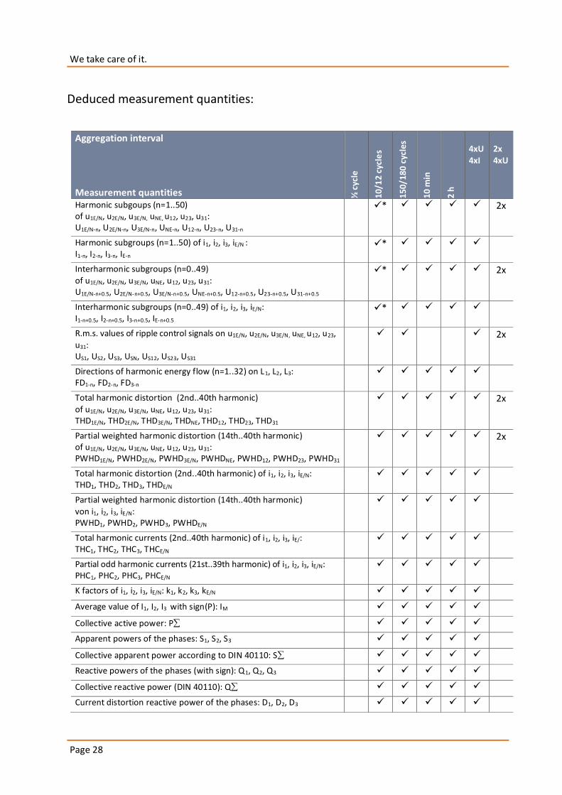
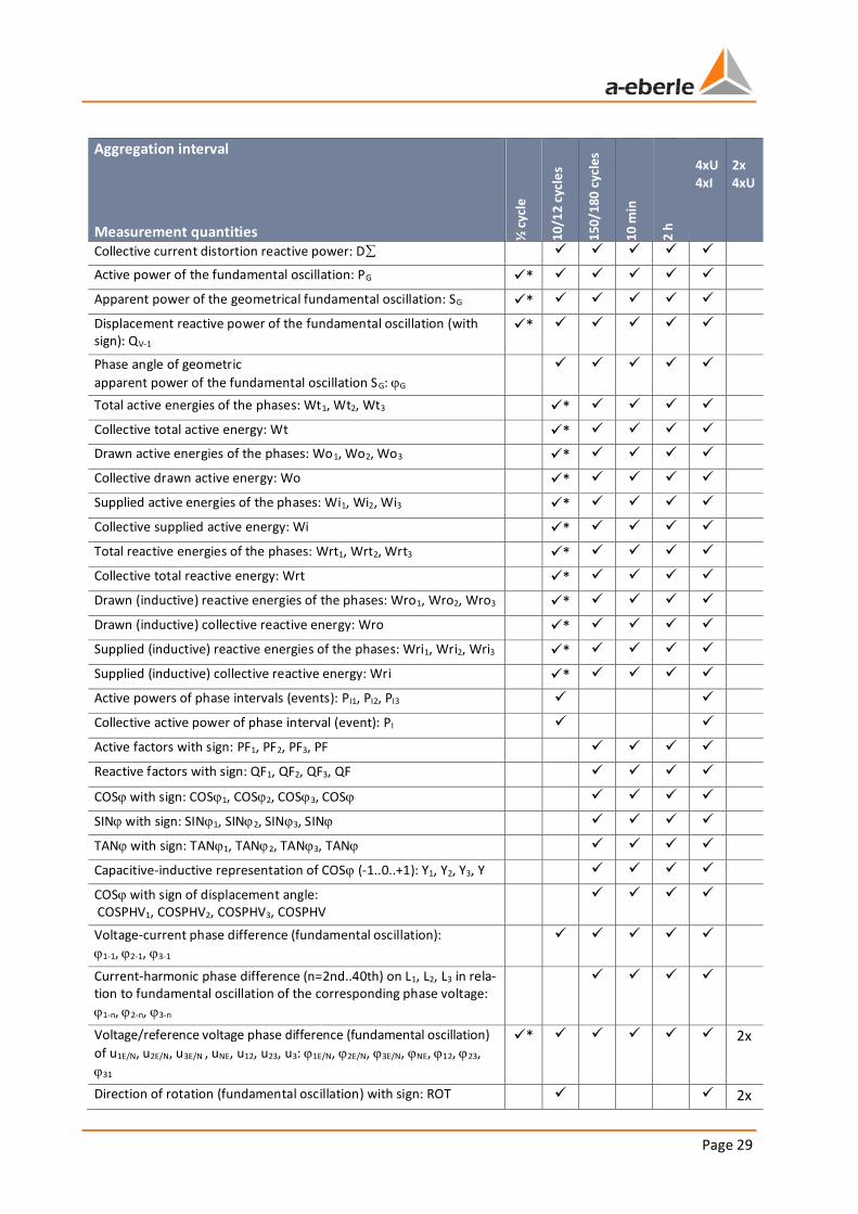
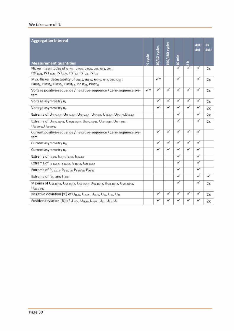
Deduced measurement quantities:
Aggregation interval Measurement quantities ½
cyc
le
10
/12
cyc
les
15
0/1
80
cyc
les
10
min
2 h
4xU
4xI
2x
4xU
Harmonic subgoups (n=1..50) of u1E/N, u2E/N, u3E/N, uNE, u12, u23, u31: U1E/N-n, U2E/N-n, U3E/N-n, UNE-n, U12-n, U23-n, U31-n
* 2x
Harmonic subgroups (n=1..50) of i1, i2, i3, iE/N : I1-n, I2-n, I3-n, IE-n
*
Interharmonic subgroups (n=0..49) of u1E/N, u2E/N, u3E/N, uNE, u12, u23, u31: U1E/N-n+0.5, U2E/N-n+0.5, U3E/N-n+0.5, UNE-n+0.5, U12-n+0.5, U23-n+0.5, U31-n+0.5
* 2x
Interharmonic subgroups (n=0..49) of i1, i2, i3, iE/N: I1-n+0.5, I2-n+0.5, I3-n+0.5, IE-n+0.5
*
R.m.s. values of ripple control signals on u1E/N, u2E/N, u3E/N, uNE, u12, u23, u31: US1, US2, US3, USN, US12, US23, US31
2x
Directions of harmonic energy flow (n=1..32) on L1, L2, L3: FD1-n, FD2-n, FD3-n
Total harmonic distortion (2nd..40th harmonic)
of u1E/N, u2E/N, u3E/N, uNE, u12, u23, u31: THD1E/N, THD2E/N, THD3E/N, THDNE, THD12, THD23, THD31
2x
Partial weighted harmonic distortion (14th..40th harmonic) of u1E/N, u2E/N, u3E/N, uNE, u12, u23, u31: PWHD1E/N, PWHD2E/N, PWHD3E/N, PWHDNE, PWHD12, PWHD23, PWHD31
2x
Total harmonic distortion (2nd..40th harmonic) of i1, i2, i3, iE/N: THD1, THD2, THD3, THDE/N
Partial weighted harmonic distortion (14th..40th harmonic) von i1, i2, i3, iE/N: PWHD1, PWHD2, PWHD3, PWHDE/N
Total harmonic currents (2nd..40th harmonic) of i1, i2, i3, iE/: THC1, THC2, THC3, THCE/N
Partial odd harmonic currents (21st..39th harmonic) of i1, i2, i3, iE/N: PHC1, PHC2, PHC3, PHCE/N
K factors of i1, i2, i3, iE/N: k1, k2, k3, kE/N
Average value of I1, I2, I3 with sign(P): IM
Collective active power: P
Apparent powers of the phases: S1, S2, S3
Collective apparent power according to DIN 40110: S
Reactive powers of the phases (with sign): Q1, Q2, Q3
Collective reactive power (DIN 40110): Q
Current distortion reactive power of the phases: D1, D2, D3
Page 29
Aggregation interval Measurement quantities ½
cyc
le
10
/12
cyc
les
15
0/1
80
cyc
les
10
min
2 h
4xU 4xI
2x 4xU
Collective current distortion reactive power: D
Active power of the fundamental oscillation: PG *
Apparent power of the geometrical fundamental oscillation: SG *
Displacement reactive power of the fundamental oscillation (with sign): QV-1
*
Phase angle of geometric
apparent power of the fundamental oscillation SG: G
Total active energies of the phases: Wt1, Wt2, Wt3 *
Collective total active energy: Wt *
Drawn active energies of the phases: Wo1, Wo2, Wo3 *
Collective drawn active energy: Wo *
Supplied active energies of the phases: Wi1, Wi2, Wi3 *
Collective supplied active energy: Wi *
Total reactive energies of the phases: Wrt1, Wrt2, Wrt3 *
Collective total reactive energy: Wrt *
Drawn (inductive) reactive energies of the phases: Wro1, Wro2, Wro3 *
Drawn (inductive) collective reactive energy: Wro *
Supplied (inductive) reactive energies of the phases: Wri1, Wri2, Wri3 *
Supplied (inductive) collective reactive energy: Wri *
Active powers of phase intervals (events): PI1, PI2, PI3
Collective active power of phase interval (event): PI
Active factors with sign: PF1, PF2, PF3, PF
Reactive factors with sign: QF1, QF2, QF3, QF
COS with sign: COS1, COS2, COS3, COS
SIN with sign: SIN1, SIN2, SIN3, SIN
TAN with sign: TAN1, TAN2, TAN3, TAN
Capacitive-inductive representation of COS (-1..0..+1): Y1, Y2, Y3, Y
COS with sign of displacement angle: COSPHV1, COSPHV2, COSPHV3, COSPHV
Voltage-current phase difference (fundamental oscillation):
1-1, 2-1, 3-1
Current-harmonic phase difference (n=2nd..40th) on L1, L2, L3 in rela-tion to fundamental oscillation of the corresponding phase voltage:
1-n, 2-n, 3-n
Voltage/reference voltage phase difference (fundamental oscillation)
of u1E/N, u2E/N, u3E/N , uNE, u12, u23, u3: 1E/N, 2E/N, 3E/N, NE, 12, 23,
31
* 2x
Direction of rotation (fundamental oscillation) with sign: ROT 2x
We take care of it.
Page 30
Aggregation interval Measurement quantities ½
cyc
le
10
/12
cyc
les
15
0/1
80
cyc
les
10
min
2 h
4xU 4xI
2x 4xU
Flicker magnitudes of u1E/N, u2E/N, u3E/N, u12, u23, u31: PxT1E/N, PxT2E/N, PxT3E/N, PxT12, PxT23, PxT31
2x
Max. flicker detectability of u1E/N, u2E/N, u3E/N, u12, u23, u31 : Pinst1, Pinst2, Pinst3, Pinst12, Pinst23, Pinst31
* 2x
Voltage positive-sequence / negative-sequence / zero-sequence sys-tem
* 2x
Voltage asymmetry uu 2x
Voltage asymmetry u0 2x
Extrema of U1E/N-1/2, U2E/N-1/2, U3E/N-1/2, UNE-1/2, U12-1/2, U23-1/2,U31-1/2 2x
Extrema of U1E/N-10/12, U2E/N-10/12, U3E/N-10/12, UNE-10/12, U12-10/12, U23-10/12,U31-10/12
2x
Current positive-sequence / negative-sequence / zero-sequence sys-tem
Current asymmetry uu
Current asymmetry u0
Extrema of I1-1/2, I2-1/2, I3-1/2, IE/N-1/2
Extrema of I1-10/12, I2-10/12, I3-10/12, IE/N-10/12
Extrema of P1-10/12, P2-10/12, P3-10/12, P10/12
Extrema of f10s and f10/12
Maxima of US1-10/12, US2-10/12, US3-10/12, USN-10/12, US12-10/12, US23-10/12, US31-10/12
2x
Negative deviation [%] of U1E/N, U2E/N, U3E/N, U12, U23, U31 2x
Positive deviation [%] of U1E/N, U2E/N, U3E/N, U12, U23, U31 2x
Page 31
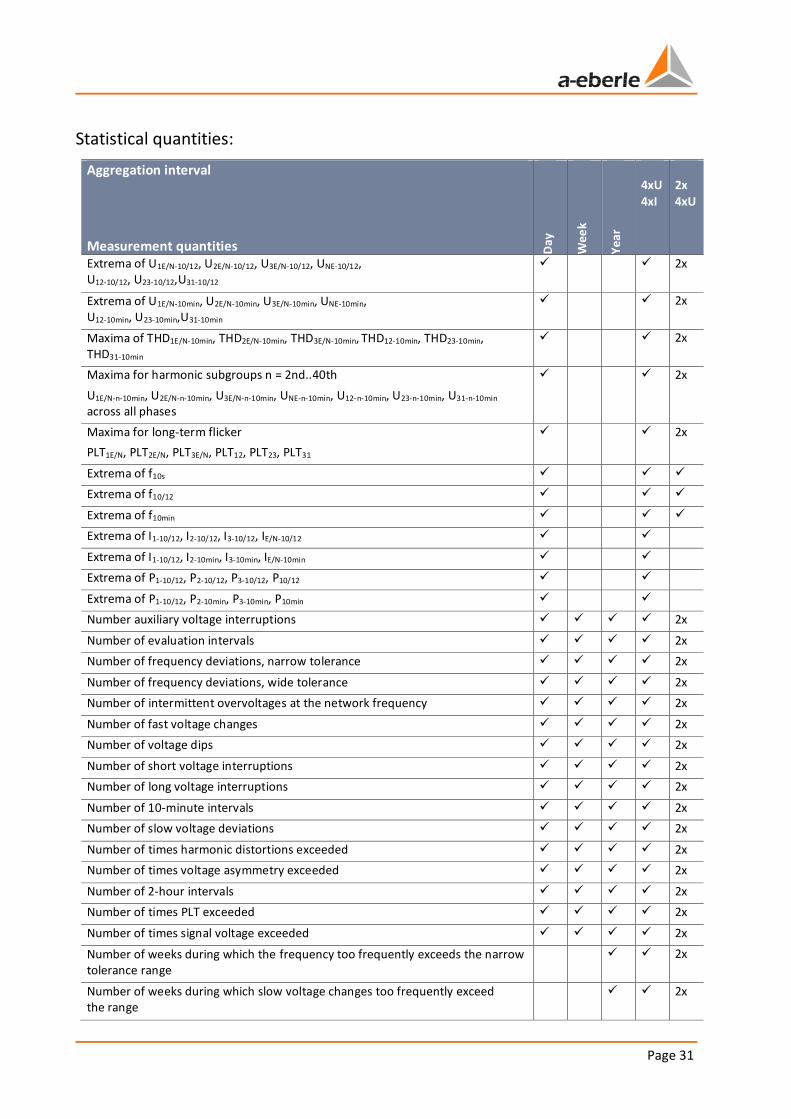
Statistical quantities:
Aggregation interval Measurement quantities D
ay
Wee
k
Yea
r
4xU
4xI
2x
4xU
Extrema of U1E/N-10/12, U2E/N-10/12, U3E/N-10/12, UNE-10/12, U12-10/12, U23-10/12,U31-10/12
2x
Extrema of U1E/N-10min, U2E/N-10min, U3E/N-10min, UNE-10min, U12-10min, U23-10min,U31-10min
2x
Maxima of THD1E/N-10min, THD2E/N-10min, THD3E/N-10min, THD12-10min, THD23-10min, THD31-10min
2x
Maxima for harmonic subgroups n = 2nd..40th
U1E/N-n-10min, U2E/N-n-10min, U3E/N-n-10min, UNE-n-10min, U12-n-10min, U23-n-10min, U31-n-10min
across all phases
2x
Maxima for long-term flicker
PLT1E/N, PLT2E/N, PLT3E/N, PLT12, PLT23, PLT31
2x
Extrema of f10s
Extrema of f10/12
Extrema of f10min
Extrema of I1-10/12, I2-10/12, I3-10/12, IE/N-10/12
Extrema of I1-10/12, I2-10min, I3-10min, IE/N-10min
Extrema of P1-10/12, P2-10/12, P3-10/12, P10/12
Extrema of P1-10/12, P2-10min, P3-10min, P10min
Number auxiliary voltage interruptions 2x
Number of evaluation intervals 2x
Number of frequency deviations, narrow tolerance 2x
Number of frequency deviations, wide tolerance 2x
Number of intermittent overvoltages at the network frequency 2x
Number of fast voltage changes 2x
Number of voltage dips 2x
Number of short voltage interruptions 2x
Number of long voltage interruptions 2x
Number of 10-minute intervals 2x
Number of slow voltage deviations 2x
Number of times harmonic distortions exceeded 2x
Number of times voltage asymmetry exceeded 2x
Number of 2-hour intervals 2x
Number of times PLT exceeded 2x
Number of times signal voltage exceeded 2x
Number of weeks during which the frequency too frequently exceeds the narrow tolerance range
2x
Number of weeks during which slow voltage changes too frequently exceed the range
2x
We take care of it.
Page 32
Aggregation interval Measurement quantities D
ay
Wee
k
Yea
r
4xU 4xI
2x 4xU
Number of weeks during which harmonic distortions too frequently exceed the range
2x
Number of weeks during which voltage asymmetry too frequently exceededs the range
2x
Number of weeks during which flicker PLT too frequently exceeds the range 2x
Number of days on which signal voltage is too frequently exceeded 2x
Time sum for auxiliary voltage interruptions 2x
Time sum for measurement time 2x
Time sum for frequency deviations, narrow tolerance 2x
Time sum for frequency deviations, wide tolerance 2x
Time sum for intermittent overvoltage at the network frequency 2x
Time sum for fast voltage changes 2x
Time sum for voltage dips 2x
Time sum for short voltage interruptions 2x
Time sum for long voltage interruptions 2x
Time sum for exceeded signal voltages 2x
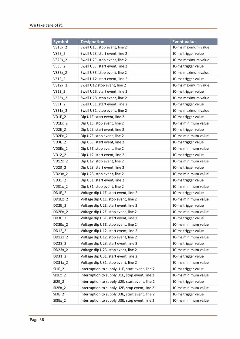
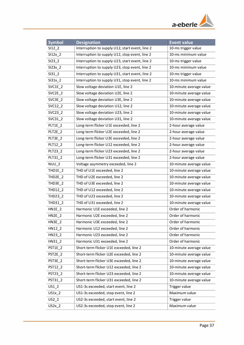
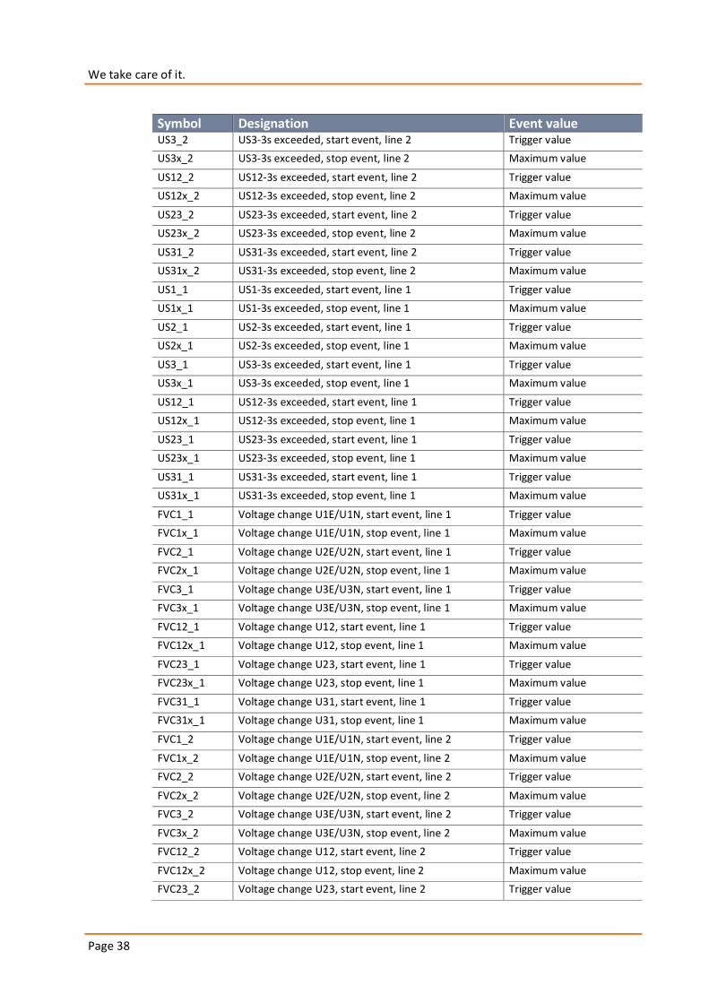
Overview of events:
Symbol Designation Event value RST System reset, start event Error code
RSTx System reset, stop event Error code
STATERR Station error flags Error flags
SYNC Frequency valid f
NOTSYNC Frequency invalid 0
TIMESET Time setting Time difference [s]
NEWDAY New day initialised Day index
BININPUT Status change at binary inputs Last status
Current status
COM1ERR Error COM1 Error code
TRG_RX External trigger, receive 0
COM2ERR Error COM2 Error code
DFN Frequency deviation (narrow tolerance), start event 10-second trigger value
DFNx Frequency deviation (narrow tolerance) , stop event 10-second extreme value
DFW Frequency deviation (wide tolerance), start event 10-second trigger value
DFWx Frequency deviation (wide tolerance) , stop event 10-second extreme value
TRG_TX Ext. trigger, send Bit ID
TRG_W0 Status change in trigger word#0 Status word
Page 33
Symbol Designation Event value TRG_W1 Status change in trigger word#1 Status word
TRG_W2 Status change in trigger word#2 Status word
TEDUR Duration of transient event [s] Event duration [s]
RUN_REC Status change in recording of data classes Status word
BINOUTPUT Status change at binary outputs Last status Current status
TIMESYNC Status change, external time synchronisation Status word
EVNTOF DSP event buffer overflow Level
RSTEVAL_1 Reset event evaluation, line 1 0
EVAL_1 Event evaluation, start event, line 1 0
EVALx_1 Event evaluation, stop event, line 1 0
RECA_1 New recording in recorder A1 "Absolute index"
RECS_1 New recording in recorder S1 "Absolute index"
RECB_1 New recording in recorder B1 "Absolute index"
TRANSNOSTIC Status message Transnostic Status word
TEDUR Duration of transient event [s] Event duration [s]
RECC_1 New recording in recorder C1 "Absolute index"
OV1E_1 Overvoltage U1E, start event, line 1 10-ms trigger value
OV1Ex_1 Overvoltage U1E, stop event, line 1 10-ms maximum value
OV2E_1 Overvoltage U2E, start event, line 1 10-ms trigger value
OV2Ex_1 Overvoltage U2E, stop event, line 1 10-ms maximum value
OV3E_1 Overvoltage U3E, start event, line 1 10-ms trigger value
OV3Ex_1 Overvoltage U3E, stop event, line 1 10-ms maximum value
OVNE_1 Overvoltage UNE, start event, line 1 10-ms trigger value
OVNEx_1 Overvoltage UNE, stop event, line 1 10-ms maximum value
VS1E_1 Swell U1E, start event, line 1 10-ms trigger value
VS1Ex_1 Swell U1E, stop event, line 1 10-ms maximum value
VS2E_1 Swell U2E, start event, line 1 10-ms trigger value
VS2Ex_1 Swell U2E, stop event, line 1 10-ms maximum value
VS3E_1 Swell U3E, start event, line 1 10-ms trigger value
VS3Ex_1 Swell U3E, stop event, line 1 10-ms maximum value
VS12_1 Swell U12, start event, line 1 10-ms trigger value
VS12x_1 Swell U12, stop event, line 1 10-ms maximum value
VS23_1 Swell U23, start event, line 1 10-ms trigger value
VS23x_1 Swell U23, stop event, line 1 10-ms maximum value
VS31_1 Swell U31, start event, line 1 10-ms trigger value
VS31x_1 Swell U31, stop event, line 1 10-ms maximum value
VD1E_1 Dip U1E, start event, line 1 10-ms trigger value
VD1Ex_1 Dip U1E, stop event, line 1 10-ms minimum value
VD2E_1 Dip U2E, start event, line 1 10-ms trigger value
VD2Ex_1 Dip U2E, stop event, line 1 10-ms minimum value
VD3E_1 Dip U3E, start event, line 1 10-ms trigger value
We take care of it.
Page 34
Symbol Designation Event value VD3Ex_1 Dip U3E, stop event, line 1 10-ms minimum value
VD12_1 Dip U12, start event, line 1 10-ms trigger value
VD12x_1 Dip U12, stop event, line 1 10-ms minimum value
VD23_1 Dip U23, start event, line 1 10-ms trigger value
VD23x_1 Dip U23, stop event, line 1 10-ms minimum value
VD31_1 Dip U31, start event, line 1 10-ms trigger value
VD31x_1 Dip U31, stop event, line 1 10-ms minimum value
DD1E_1 Voltage dip U1E, start event, line 1 10-ms trigger value
DD1Ex_1 Voltage dip U1E, stop event, line 1 10-ms minimum value
DD2E_1 Voltage dip U2E, start event, line 1 10-ms trigger value
DD2Ex_1 Voltage dip U2E, stop event, line 1 10-ms minimum value
DD3E_1 Voltage dip U3E, start event, line 1 10-ms trigger value
DD3Ex_1 Voltage dip U3E, stop event, line 1 10-ms minimum value
DD12_1 Voltage dip U12, start event, line 1 10-ms trigger value
DD12x_1 Voltage dip U12, stop event, line 1 10-ms minimum value
DD23_1 Voltage dip U23, start event, line 1 10-ms trigger value
DD23x_1 Voltage dip U23, stop event, line 1 10-ms minimum value
DD31_1 Voltage dip U31, start event, line 1 10-ms trigger value
DD31x_1 Voltage dip U31, stop event, line 1 10-ms minimum value
SI1E_1 Interruption to supply U1E, start event, line 1 10-ms trigger value
SI1Ex_1 Interruption to supply U1E, stop event, line 1 10-ms minimum value
SI2E_1 Interruption to supply U2E, start event, line 1 10-ms trigger value
SI2Ex_1 Interruption to supply U2E, stop event, line 1 10-ms minimum value
SI3E_1 Interruption to supply U3E, start event, line 1 10-ms trigger value
SI3Ex_1 Interruption to supply U3E, stop event, line 1 10-ms minimum value
SI12_1 Interruption to supply U12, start event, line 1 10-ms trigger value
SI12x_1 Interruption to supply U12, stop event, line 1 10-ms minimum value
SI23_1 Interruption to supply U23, start event, line 1 10-ms trigger value
SI23x_1 Interruption to supply U23, stop event, line 1 10-ms minimum value
SI31_1 Interruption to supply U31, start event, line 1 10-ms trigger value
SI31x_1 Interruption to supply U31, stop event, line 1 10-ms minimum value
SVC1E_1 Slow voltage deviation U1E, line 1 10-minute average value
SVC2E_1 Slow voltage deviation U2E, line 1 10-minute average value
SVC3E_1 Slow voltage deviation U3E, line 1 10-minute average value
SVC12_1 Slow voltage deviation U12, line 1 10-minute average value
SVC23_1 Slow voltage deviation U23, line 1 10-minute average value
SVC31_1 Slow voltage deviation U31, line 1 10-minute average value
PLT1E_1 Long-term flicker U1E exceeded, line 1 2-hour average value
PLT2E_1 Long-term flicker U2E exceeded, line 1 2-hour average value
PLT3E_1 Long-term flicker U3E exceeded, line 1 2-hour average value
PLT12_1 Long-term flicker U12 exceeded, line 1 2-hour average value
Page 35
Symbol Designation Event value PLT23_1 Long-term flicker U23 exceeded, line 1 2-hour average value
PLT31_1 Long-term flicker U31 exceeded, line 1 2-hour average value
NUU_1 Voltage asymmetry exceeded, line 1 10-minute average value
THD1EV_1 THD of U1E exceeded, line 1 10-minute average value
THD2EV_1 THD of U2E exceeded, line 1 10-minute average value
THD3EV_1 THD of U3E exceeded, line 1 10-minute average value
THD12V_1 THD of U12 exceeded, line 1 10-minute average value
THD23V_1 THD of U23 exceeded, line 1 10-minute average value
THD31V_1 THD of U31 exceeded, line 1 10-minute average value
HN1EV_1 Harmonic U1E exceeded, line 1 Order of harmonic
HN2EV_1 Harmonic U2E exceeded, line 1 Order of harmonic
HN3EV_1 Harmonic U3E exceeded, line 1 Order of harmonic
HN12V_1 Harmonic U12 exceeded, line 1 Order of harmonic
HN23V_1 Harmonic U23 exceeded, line 1 Order of harmonic
HN31V_1 Harmonic U31 exceeded, line 1 Order of harmonic
PST1E_1 Short-term flicker U1E exceeded, line 1 10-minute average value
PST2E_1 Short-term flicker U2E exceeded, line 1 10-minute average value
PST3E_1 Short-term flicker U3E exceeded, line 1 10-minute average value
PST12_1 Short-term flicker U12 exceeded, line 1 10-minute average value
PST23_1 Short-term flicker U23 exceeded, line 1 10-minute average value
PST31_1 Short-term flicker U31 exceeded, line 1 10-minute average value
PI1 Interval active power L1 Interval average value
PI2 Interval active power L2 Interval average value
PI3 Interval active power L3 Interval average value
PI Interval active power of the network Interval average value
RSTEVAL_2 Reset event evaluation, line 2 0
EVAL_2 Event evaluation, start event, line 2 0
EVALx_2 Event evaluation, stop event, line 2 0
RECA_2 New recording in recorder A2 "Absolute index"
RECS_2 New recording in recorder S2 "Absolute index"
RECB_2 New recording in recorder B2 "Absolute index"
RECC_2 New recording in recorder C2 "Absolute index"
OV1E_2 Overvoltage U1E, start event, line 2 10-ms trigger value
OV1Ex_2 Overvoltage U1E, stop event, line 2 10-ms maximum value
OV2E_2 Overvoltage U2E, start event, line 2 10-ms trigger value
OV2Ex_2 Overvoltage U2E, stop event, line 2 10-ms maximum value
OV3E_2 Overvoltage U3E, start event, line 2 10-ms trigger value
OV3Ex_2 Overvoltage U3E, stop event, line 2 10-ms maximum value
OVNE_2 Overvoltage UNE, start event, line 2 10-ms trigger value
OVNEx_2 Overvoltage UNE, stop event, line 2 10-ms maximum value
VS1E_2 Swell U1E, start event, line 2 10-ms trigger value
We take care of it.
Page 36
Symbol Designation Event value VS1Ex_2 Swell U1E, stop event, line 2 10-ms maximum value
VS2E_2 Swell U2E, start event, line 2 10-ms trigger value
VS2Ex_2 Swell U2E, stop event, line 2 10-ms maximum value
VS3E_2 Swell U3E, start event, line 2 10-ms trigger value
VS3Ex_2 Swell U3E, stop event, line 2 10-ms maximum value
VS12_2 Swell U12, start event, line 2 10-ms trigger value
VS12x_2 Swell U12 stop event, line 2 10-ms maximum value
VS23_2 Swell U23, start event, line 2 10-ms trigger value
VS23x_2 Swell U23, stop event, line 2 10-ms maximum value
VS31_2 Swell U31, start event, line 2 10-ms trigger value
VS31x_2 Swell U31, stop event, line 2 10-ms maximum value
VD1E_2 Dip U1E, start event, line 2 10-ms trigger value
VD1Ex_2 Dip U1E, stop event, line 2 10-ms minimum value
VD2E_2 Dip U2E, start event, line 2 10-ms trigger value
VD2Ex_2 Dip U2E, stop event, line 2 10-ms minimum value
VD3E_2 Dip U3E, start event, line 2 10-ms trigger value
VD3Ex_2 Dip U3E, stop event, line 2 10-ms minimum value
VD12_2 Dip U12, start event, line 2 10-ms trigger value
VD12x_2 Dip U12, stop event, line 2 10-ms minimum value
VD23_2 Dip U23, start event, line 2 10-ms trigger value
VD23x_2 Dip U23, stop event, line 2 10-ms minimum value
VD31_2 Dip U31, start event, line 2 10-ms trigger value
VD31x_2 Dip U31, stop event, line 2 10-ms minimum value
DD1E_2 Voltage dip U1E, start event, line 2 10-ms trigger value
DD1Ex_2 Voltage dip U1E, stop event, line 2 10-ms minimum value
DD2E_2 Voltage dip U2E, start event, line 2 10-ms trigger value
DD2Ex_2 Voltage dip U2E, stop event, line 2 10-ms minimum value
DD3E_2 Voltage dip U3E, start event, line 2 10-ms trigger value
DD3Ex_2 Voltage dip U3E, stop event, line 2 10-ms minimum value
DD12_2 Voltage dip U12, start event, line 2 10-ms trigger value
DD12x_2 Voltage dip U12, stop event, line 2 10-ms minimum value
DD23_2 Voltage dip U23, start event, line 2 10-ms trigger value
DD23x_2 Voltage dip U23, stop event, line 2 10-ms minimum value
DD31_2 Voltage dip U31, start event, line 2 10-ms trigger value
DD31x_2 Voltage dip U31, stop event, line 2 10-ms minimum value
SI1E_2 Interruption to supply U1E, start event, line 2 10-ms trigger value
SI1Ex_2 Interruption to supply U1E, stop event, line 2 10-ms minimum value
SI2E_2 Interruption to supply U2E, start event, line 2 10-ms trigger value
SI2Ex_2 Interruption to supply U2E, stop event, line 2 10-ms minimum value
SI3E_2 Interruption to supply U3E, start event, line 2 10-ms trigger value
SI3Ex_2 Interruption to supply U3E, stop event, line 2 10-ms minimum value
Page 37
Symbol Designation Event value SI12_2 Interruption to supply U12, start event, line 2 10-ms trigger value
SI12x_2 Interruption to supply U12, stop event, line 2 10-ms minimum value
SI23_2 Interruption to supply U23, start event, line 2 10-ms trigger value
SI23x_2 Interruption to supply U23, stop event, line 2 10-ms minimum value
SI31_2 Interruption to supply U31, start event, line 2 10-ms trigger value
SI31x_2 Interruption to supply U31, stop event, line 2 10-ms minimum value
SVC1E_2 Slow voltage deviation U1E, line 2 10-minute average value
SVC2E_2 Slow voltage deviation U2E, line 2 10-minute average value
SVC3E_2 Slow voltage deviation U3E, line 2 10-minute average value
SVC12_2 Slow voltage deviation U12, line 2 10-minute average value
SVC23_2 Slow voltage deviation U23, line 2 10-minute average value
SVC31_2 Slow voltage deviation U31, line 2 10-minute average value
PLT1E_2 Long-term flicker U1E exceeded, line 2 2-hour average value
PLT2E_2 Long-term flicker U2E exceeded, line 2 2-hour average value
PLT3E_2 Long-term flicker U3E exceeded, line 2 2-hour average value
PLT12_2 Long-term flicker U12 exceeded, line 2 2-hour average value
PLT23_2 Long-term flicker U23 exceeded, line 2 2-hour average value
PLT31_2 Long-term flicker U31 exceeded, line 2 2-hour average value
NUU_2 Voltage asymmetry exceeded, line 2 10-minute average value
THD1E_2 THD of U1E exceeded, line 2 10-minute average value
THD2E_2 THD of U2E exceeded, line 2 10-minute average value
THD3E_2 THD of U3E exceeded, line 2 10-minute average value
THD12_2 THD of U12 exceeded, line 2 10-minute average value
THD23_2 THD of U23 exceeded, line 2 10-minute average value
THD31_2 THD of U31 exceeded, line 2 10-minute average value
HN1E_2 Harmonic U1E exceeded, line 2 Order of harmonic
HN2E_2 Harmonic U2E exceeded, line 2 Order of harmonic
HN3E_2 Harmonic U3E exceeded, line 2 Order of harmonic
HN12_2 Harmonic U12 exceeded, line 2 Order of harmonic
HN23_2 Harmonic U23 exceeded, line 2 Order of harmonic
HN31_2 Harmonic U31 exceeded, line 2 Order of harmonic
PST1E_2 Short-term flicker U1E exceeded, line 2 10-minute average value
PST2E_2 Short-term flicker U2E exceeded, line 2 10-minute average value
PST3E_2 Short-term flicker U3E exceeded, line 2 10-minute average value
PST12_2 Short-term flicker U12 exceeded, line 2 10-minute average value
PST23_2 Short-term flicker U23 exceeded, line 2 10-minute average value
PST31_2 Short-term flicker U31 exceeded, line 2 10-minute average value
US1_2 US1-3s exceeded, start event, line 2 Trigger value
US1x_2 US1-3s exceeded, stop event, line 2 Maximum value
US2_2 US2-3s exceeded, start event, line 2 Trigger value
US2x_2 US2-3s exceeded, stop event, line 2 Maximum value
We take care of it.
Page 38
Symbol Designation Event value US3_2 US3-3s exceeded, start event, line 2 Trigger value
US3x_2 US3-3s exceeded, stop event, line 2 Maximum value
US12_2 US12-3s exceeded, start event, line 2 Trigger value
US12x_2 US12-3s exceeded, stop event, line 2 Maximum value
US23_2 US23-3s exceeded, start event, line 2 Trigger value
US23x_2 US23-3s exceeded, stop event, line 2 Maximum value
US31_2 US31-3s exceeded, start event, line 2 Trigger value
US31x_2 US31-3s exceeded, stop event, line 2 Maximum value
US1_1 US1-3s exceeded, start event, line 1 Trigger value
US1x_1 US1-3s exceeded, stop event, line 1 Maximum value
US2_1 US2-3s exceeded, start event, line 1 Trigger value
US2x_1 US2-3s exceeded, stop event, line 1 Maximum value
US3_1 US3-3s exceeded, start event, line 1 Trigger value
US3x_1 US3-3s exceeded, stop event, line 1 Maximum value
US12_1 US12-3s exceeded, start event, line 1 Trigger value
US12x_1 US12-3s exceeded, stop event, line 1 Maximum value
US23_1 US23-3s exceeded, start event, line 1 Trigger value
US23x_1 US23-3s exceeded, stop event, line 1 Maximum value
US31_1 US31-3s exceeded, start event, line 1 Trigger value
US31x_1 US31-3s exceeded, stop event, line 1 Maximum value
FVC1_1 Voltage change U1E/U1N, start event, line 1 Trigger value
FVC1x_1 Voltage change U1E/U1N, stop event, line 1 Maximum value
FVC2_1 Voltage change U2E/U2N, start event, line 1 Trigger value
FVC2x_1 Voltage change U2E/U2N, stop event, line 1 Maximum value
FVC3_1 Voltage change U3E/U3N, start event, line 1 Trigger value
FVC3x_1 Voltage change U3E/U3N, stop event, line 1 Maximum value
FVC12_1 Voltage change U12, start event, line 1 Trigger value
FVC12x_1 Voltage change U12, stop event, line 1 Maximum value
FVC23_1 Voltage change U23, start event, line 1 Trigger value
FVC23x_1 Voltage change U23, stop event, line 1 Maximum value
FVC31_1 Voltage change U31, start event, line 1 Trigger value
FVC31x_1 Voltage change U31, stop event, line 1 Maximum value
FVC1_2 Voltage change U1E/U1N, start event, line 2 Trigger value
FVC1x_2 Voltage change U1E/U1N, stop event, line 2 Maximum value
FVC2_2 Voltage change U2E/U2N, start event, line 2 Trigger value
FVC2x_2 Voltage change U2E/U2N, stop event, line 2 Maximum value
FVC3_2 Voltage change U3E/U3N, start event, line 2 Trigger value
FVC3x_2 Voltage change U3E/U3N, stop event, line 2 Maximum value
FVC12_2 Voltage change U12, start event, line 2 Trigger value
FVC12x_2 Voltage change U12, stop event, line 2 Maximum value
FVC23_2 Voltage change U23, start event, line 2 Trigger value
Page 39
Symbol Designation Event value FVC23x_2 Voltage change U23, stopt event, line 2 Maximum value
FVC31_2 Voltage change U31, start event, line 2 Trigger value
FVC31x_2 Voltage change U31, stop event, line 2 Maximum value
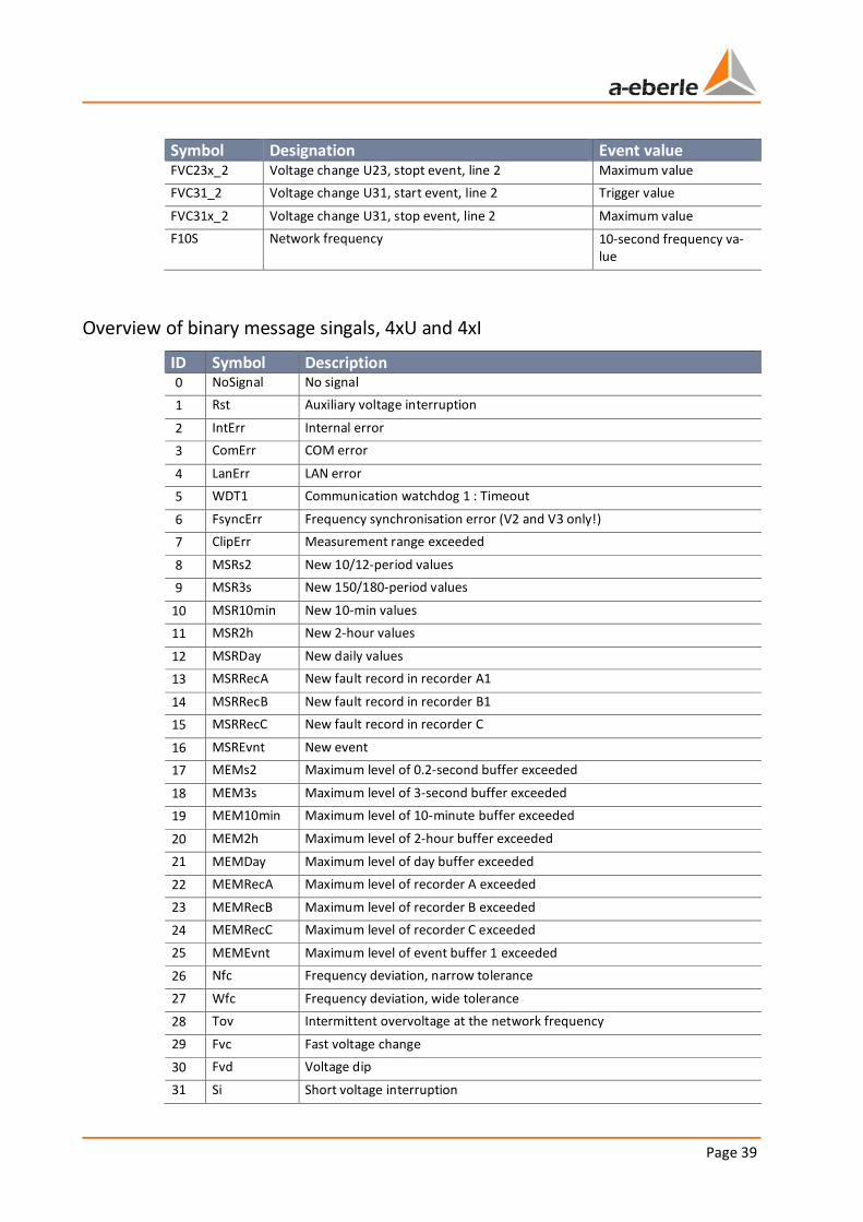
F10S Network frequency 10-second frequency va-lue
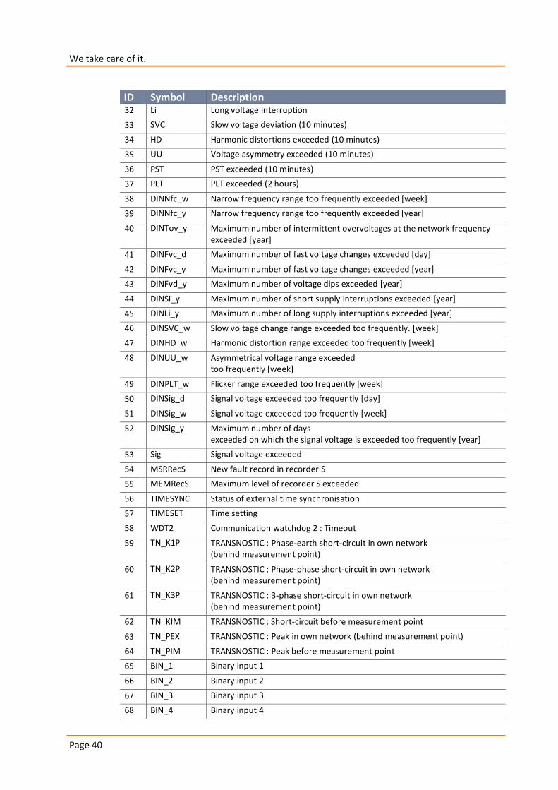
Overview of binary message singals, 4xU and 4xI
ID Symbol Description 0 NoSignal No signal
1 Rst Auxiliary voltage interruption
2 IntErr Internal error
3 ComErr COM error
4 LanErr LAN error
5 WDT1 Communication watchdog 1 : Timeout
6 FsyncErr Frequency synchronisation error (V2 and V3 only!)
7 ClipErr Measurement range exceeded
8 MSRs2 New 10/12-period values
9 MSR3s New 150/180-period values
10 MSR10min New 10-min values
11 MSR2h New 2-hour values
12 MSRDay New daily values
13 MSRRecA New fault record in recorder A1
14 MSRRecB New fault record in recorder B1
15 MSRRecC New fault record in recorder C
16 MSREvnt New event
17 MEMs2 Maximum level of 0.2-second buffer exceeded
18 MEM3s Maximum level of 3-second buffer exceeded
19 MEM10min Maximum level of 10-minute buffer exceeded
20 MEM2h Maximum level of 2-hour buffer exceeded
21 MEMDay Maximum level of day buffer exceeded
22 MEMRecA Maximum level of recorder A exceeded
23 MEMRecB Maximum level of recorder B exceeded
24 MEMRecC Maximum level of recorder C exceeded
25 MEMEvnt Maximum level of event buffer 1 exceeded
26 Nfc Frequency deviation, narrow tolerance
27 Wfc Frequency deviation, wide tolerance
28 Tov Intermittent overvoltage at the network frequency
29 Fvc Fast voltage change
30 Fvd Voltage dip
31 Si Short voltage interruption
We take care of it.
Page 40
ID Symbol Description 32 Li Long voltage interruption
33 SVC Slow voltage deviation (10 minutes)
34 HD Harmonic distortions exceeded (10 minutes)
35 UU Voltage asymmetry exceeded (10 minutes)
36 PST PST exceeded (10 minutes)
37 PLT PLT exceeded (2 hours)
38 DINNfc_w Narrow frequency range too frequently exceeded [week]
39 DINNfc_y Narrow frequency range too frequently exceeded [year]
40 DINTov_y Maximum number of intermittent overvoltages at the network frequency exceeded [year]
41 DINFvc_d Maximum number of fast voltage changes exceeded [day]
42 DINFvc_y Maximum number of fast voltage changes exceeded [year]
43 DINFvd_y Maximum number of voltage dips exceeded [year]
44 DINSi_y Maximum number of short supply interruptions exceeded [year]
45 DINLi_y Maximum number of long supply interruptions exceeded [year]
46 DINSVC_w Slow voltage change range exceeded too frequently. [week]
47 DINHD_w Harmonic distortion range exceeded too frequently [week]
48 DINUU_w Asymmetrical voltage range exceeded too frequently [week]
49 DINPLT_w Flicker range exceeded too frequently [week]
50 DINSig_d Signal voltage exceeded too frequently [day]
51 DINSig_w Signal voltage exceeded too frequently [week]
52 DINSig_y Maximum number of days exceeded on which the signal voltage is exceeded too frequently [year]
53 Sig Signal voltage exceeded
54 MSRRecS New fault record in recorder S
55 MEMRecS Maximum level of recorder S exceeded
56 TIMESYNC Status of external time synchronisation
57 TIMESET Time setting
58 WDT2 Communication watchdog 2 : Timeout
59 TN_K1P TRANSNOSTIC : Phase-earth short-circuit in own network (behind measurement point)
60 TN_K2P TRANSNOSTIC : Phase-phase short-circuit in own network (behind measurement point)
61 TN_K3P TRANSNOSTIC : 3-phase short-circuit in own network (behind measurement point)
62 TN_KIM TRANSNOSTIC : Short-circuit before measurement point
63 TN_PEX TRANSNOSTIC : Peak in own network (behind measurement point)
64 TN_PIM TRANSNOSTIC : Peak before measurement point
65 BIN_1 Binary input 1
66 BIN_2 Binary input 2
67 BIN_3 Binary input 3
68 BIN_4 Binary input 4
Page 41
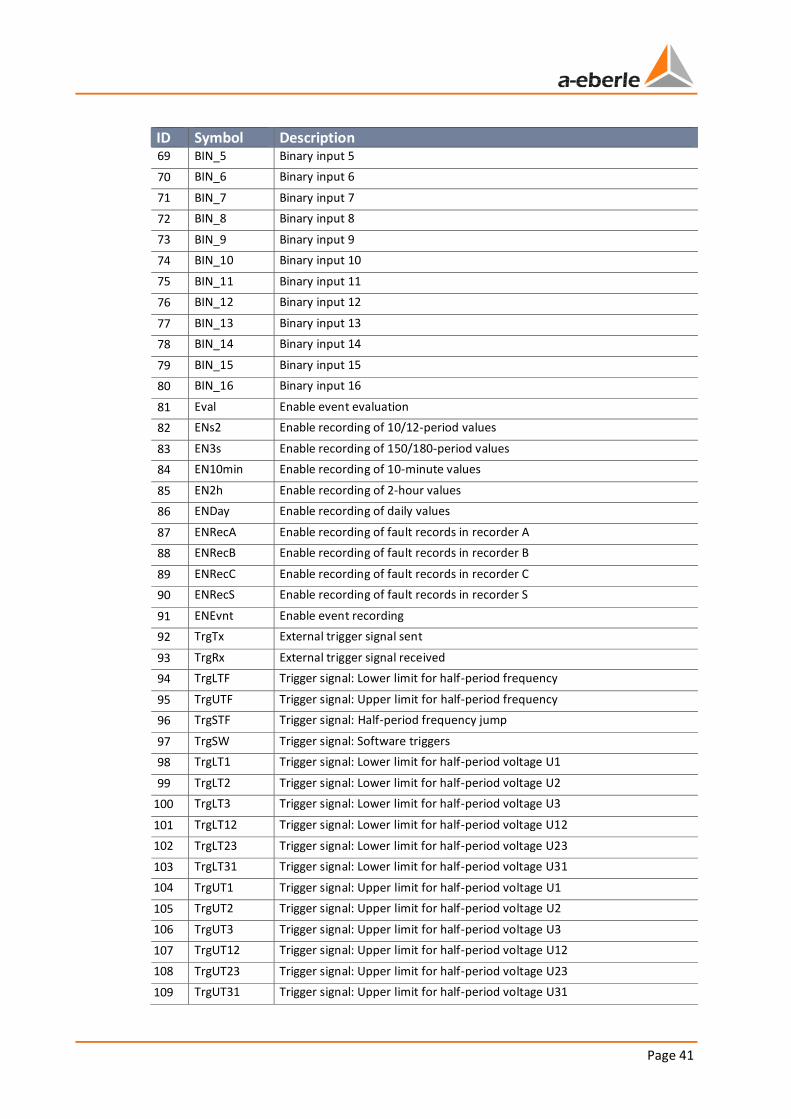
ID Symbol Description 69 BIN_5 Binary input 5
70 BIN_6 Binary input 6
71 BIN_7 Binary input 7
72 BIN_8 Binary input 8
73 BIN_9 Binary input 9
74 BIN_10 Binary input 10
75 BIN_11 Binary input 11
76 BIN_12 Binary input 12
77 BIN_13 Binary input 13
78 BIN_14 Binary input 14
79 BIN_15 Binary input 15
80 BIN_16 Binary input 16
81 Eval Enable event evaluation
82 ENs2 Enable recording of 10/12-period values
83 EN3s Enable recording of 150/180-period values
84 EN10min Enable recording of 10-minute values
85 EN2h Enable recording of 2-hour values
86 ENDay Enable recording of daily values
87 ENRecA Enable recording of fault records in recorder A
88 ENRecB Enable recording of fault records in recorder B
89 ENRecC Enable recording of fault records in recorder C
90 ENRecS Enable recording of fault records in recorder S
91 ENEvnt Enable event recording
92 TrgTx External trigger signal sent
93 TrgRx External trigger signal received
94 TrgLTF Trigger signal: Lower limit for half-period frequency
95 TrgUTF Trigger signal: Upper limit for half-period frequency
96 TrgSTF Trigger signal: Half-period frequency jump
97 TrgSW Trigger signal: Software triggers
98 TrgLT1 Trigger signal: Lower limit for half-period voltage U1
99 TrgLT2 Trigger signal: Lower limit for half-period voltage U2
100 TrgLT3 Trigger signal: Lower limit for half-period voltage U3
101 TrgLT12 Trigger signal: Lower limit for half-period voltage U12
102 TrgLT23 Trigger signal: Lower limit for half-period voltage U23
103 TrgLT31 Trigger signal: Lower limit for half-period voltage U31
104 TrgUT1 Trigger signal: Upper limit for half-period voltage U1
105 TrgUT2 Trigger signal: Upper limit for half-period voltage U2
106 TrgUT3 Trigger signal: Upper limit for half-period voltage U3
107 TrgUT12 Trigger signal: Upper limit for half-period voltage U12
108 TrgUT23 Trigger signal: Upper limit for half-period voltage U23
109 TrgUT31 Trigger signal: Upper limit for half-period voltage U31
We take care of it.
Page 42
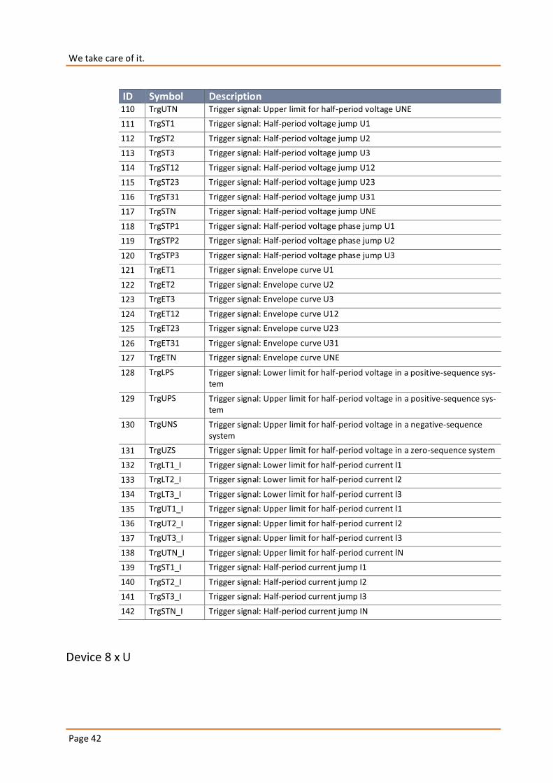
ID Symbol Description 110 TrgUTN Trigger signal: Upper limit for half-period voltage UNE
111 TrgST1 Trigger signal: Half-period voltage jump U1
112 TrgST2 Trigger signal: Half-period voltage jump U2
113 TrgST3 Trigger signal: Half-period voltage jump U3
114 TrgST12 Trigger signal: Half-period voltage jump U12
115 TrgST23 Trigger signal: Half-period voltage jump U23
116 TrgST31 Trigger signal: Half-period voltage jump U31
117 TrgSTN Trigger signal: Half-period voltage jump UNE
118 TrgSTP1 Trigger signal: Half-period voltage phase jump U1
119 TrgSTP2 Trigger signal: Half-period voltage phase jump U2
120 TrgSTP3 Trigger signal: Half-period voltage phase jump U3
121 TrgET1 Trigger signal: Envelope curve U1
122 TrgET2 Trigger signal: Envelope curve U2
123 TrgET3 Trigger signal: Envelope curve U3
124 TrgET12 Trigger signal: Envelope curve U12
125 TrgET23 Trigger signal: Envelope curve U23
126 TrgET31 Trigger signal: Envelope curve U31
127 TrgETN Trigger signal: Envelope curve UNE
128 TrgLPS Trigger signal: Lower limit for half-period voltage in a positive-sequence sys-tem
129 TrgUPS Trigger signal: Upper limit for half-period voltage in a positive-sequence sys-tem
130 TrgUNS Trigger signal: Upper limit for half-period voltage in a negative-sequence system
131 TrgUZS Trigger signal: Upper limit for half-period voltage in a zero-sequence system
132 TrgLT1_I Trigger signal: Lower limit for half-period current l1
133 TrgLT2_I Trigger signal: Lower limit for half-period current l2
134 TrgLT3_I Trigger signal: Lower limit for half-period current l3
135 TrgUT1_I Trigger signal: Upper limit for half-period current l1
136 TrgUT2_I Trigger signal: Upper limit for half-period current l2
137 TrgUT3_I Trigger signal: Upper limit for half-period current l3
138 TrgUTN_I Trigger signal: Upper limit for half-period current lN
139 TrgST1_I Trigger signal: Half-period current jump I1
140 TrgST2_I Trigger signal: Half-period current jump I2
141 TrgST3_I Trigger signal: Half-period current jump I3
142 TrgSTN_I Trigger signal: Half-period current jump IN
Device 8 x U
Page 43
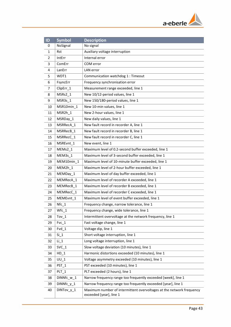
ID Symbol Description 0 NoSignal No signal
1 Rst Auxiliary voltage interruption
2 IntErr Internal error
3 ComErr COM error
4 LanErr LAN error
5 WDT1 Communication watchdog 1 : Timeout
6 FsyncErr Frequency synchronisation error
7 ClipErr_1 Measurement range exceeded, line 1
8 MSRs2_1 New 10/12-period values, line 1
9 MSR3s_1 New 150/180-period values, line 1
10 MSR10min_1 New 10-min values, line 1
11 MSR2h_1 New 2-hour values, line 1
12 MSRDay_1 New daily values, line 1
13 MSRRecA_1 New fault record in recorder A, line 1
14 MSRRecB_1 New fault record in recorder B, line 1
15 MSRRecC_1 New fault record in recorder C, line 1
16 MSREvnt_1 New event, line 1
17 MEMs2_1 Maximum level of 0.2-second buffer exceeded, line 1
18 MEM3s_1 Maximum level of 3-second buffer exceeded, line 1
19 MEM10min_1 Maximum level of 10-minute buffer exceeded, line 1
20 MEM2h_1 Maximum level of 2-hour buffer exceeded, line 1
21 MEMDay_1 Maximum level of day buffer exceeded, line 1
22 MEMRecA_1 Maximum level of recorder A exceeded, line 1
23 MEMRecB_1 Maximum level of recorder B exceeded, line 1
24 MEMRecC_1 Maximum level of recorder C exceeded, line 1
25 MEMEvnt_1 Maximum level of event buffer exceeded, line 1
26 Nfc_1 Frequency change, narrow tolerance, line 1
27 Wfc_1 Frequency change, wide tolerance, line 1
28 Tov_1 Intermittent overvoltage at the network frequency, line 1
29 Fvc_1 Fast voltage change, line 1
30 Fvd_1 Voltage dip, line 1
31 Si_1 Short voltage interruption, line 1
32 Li_1 Long voltage interruption, line 1
33 SVC_1 Slow voltage deviation (10 minutes), line 1
34 HD_1 Harmonic distortions exceeded (10 minutes), line 1
35 UU_1 Voltage asymmetry exceeded (10 minutes), line 1
36 PST_1 PST exceeded (10 minutes), line 1
37 PLT_1 PLT exceeded (2 hours), line 1
38 DINNfc_w_1 Narrow frequency range too frequently exceeded [week], line 1
39 DINNfc_y_1 Narrow frequency range too frequently exceeded [year], line 1
40 DINTov_y_1 Maximum number of intermittent overvoltages at the network frequency exceeded [year], line 1
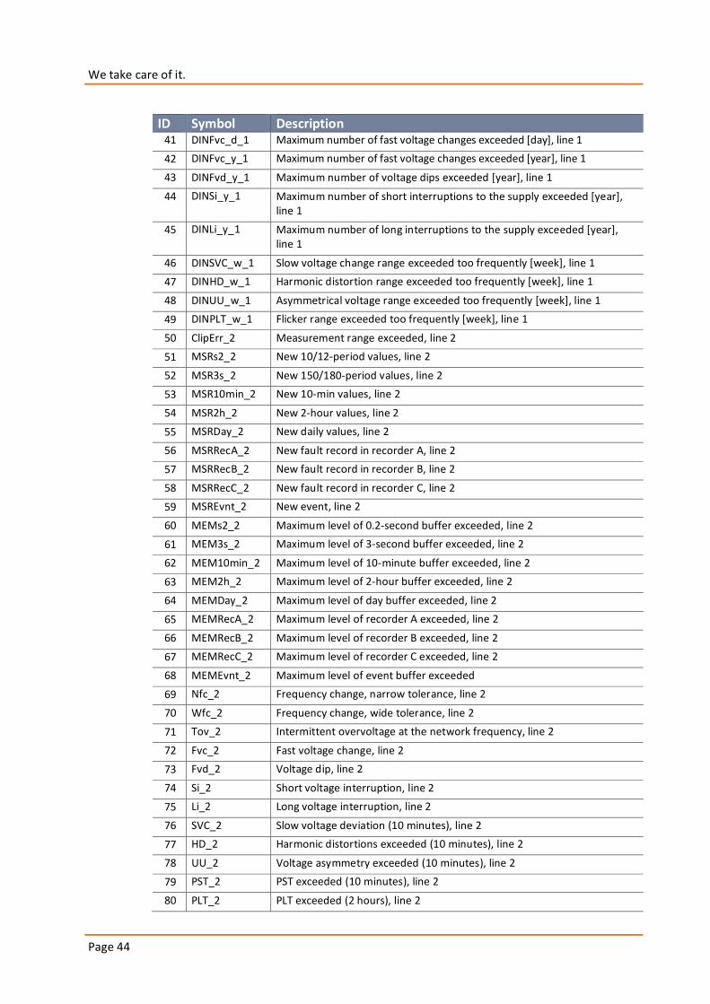
We take care of it.
Page 44
ID Symbol Description 41 DINFvc_d_1 Maximum number of fast voltage changes exceeded [day], line 1
42 DINFvc_y_1 Maximum number of fast voltage changes exceeded [year], line 1
43 DINFvd_y_1 Maximum number of voltage dips exceeded [year], line 1
44 DINSi_y_1 Maximum number of short interruptions to the supply exceeded [year], line 1
45 DINLi_y_1 Maximum number of long interruptions to the supply exceeded [year], line 1
46 DINSVC_w_1 Slow voltage change range exceeded too frequently [week], line 1
47 DINHD_w_1 Harmonic distortion range exceeded too frequently [week], line 1
48 DINUU_w_1 Asymmetrical voltage range exceeded too frequently [week], line 1
49 DINPLT_w_1 Flicker range exceeded too frequently [week], line 1
50 ClipErr_2 Measurement range exceeded, line 2
51 MSRs2_2 New 10/12-period values, line 2
52 MSR3s_2 New 150/180-period values, line 2
53 MSR10min_2 New 10-min values, line 2
54 MSR2h_2 New 2-hour values, line 2
55 MSRDay_2 New daily values, line 2
56 MSRRecA_2 New fault record in recorder A, line 2
57 MSRRecB_2 New fault record in recorder B, line 2
58 MSRRecC_2 New fault record in recorder C, line 2
59 MSREvnt_2 New event, line 2
60 MEMs2_2 Maximum level of 0.2-second buffer exceeded, line 2
61 MEM3s_2 Maximum level of 3-second buffer exceeded, line 2
62 MEM10min_2 Maximum level of 10-minute buffer exceeded, line 2
63 MEM2h_2 Maximum level of 2-hour buffer exceeded, line 2
64 MEMDay_2 Maximum level of day buffer exceeded, line 2
65 MEMRecA_2 Maximum level of recorder A exceeded, line 2
66 MEMRecB_2 Maximum level of recorder B exceeded, line 2
67 MEMRecC_2 Maximum level of recorder C exceeded, line 2
68 MEMEvnt_2 Maximum level of event buffer exceeded
69 Nfc_2 Frequency change, narrow tolerance, line 2
70 Wfc_2 Frequency change, wide tolerance, line 2
71 Tov_2 Intermittent overvoltage at the network frequency, line 2
72 Fvc_2 Fast voltage change, line 2
73 Fvd_2 Voltage dip, line 2
74 Si_2 Short voltage interruption, line 2
75 Li_2 Long voltage interruption, line 2
76 SVC_2 Slow voltage deviation (10 minutes), line 2
77 HD_2 Harmonic distortions exceeded (10 minutes), line 2
78 UU_2 Voltage asymmetry exceeded (10 minutes), line 2
79 PST_2 PST exceeded (10 minutes), line 2
80 PLT_2 PLT exceeded (2 hours), line 2
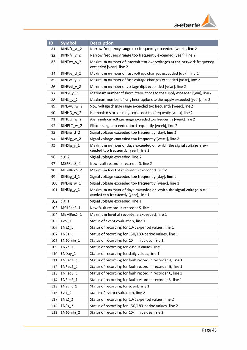
Page 45
ID Symbol Description 81 DINNfc_w_2 Narrow frequency range too frequently exceeded [week], line 2
82 DINNfc_y_2 Narrow frequency range too frequently exceeded [year], line 2
83 DINTov_y_2 Maximum number of intermittent overvoltages at the network frequency exceeded [year], line 2
84 DINFvc_d_2 Maximum number of fast voltage changes exceeded [day], line 2
85 DINFvc_y_2 Maximum number of fast voltage changes exceeded [year], line 2
86 DINFvd_y_2 Maximum number of voltage dips exceeded [year], line 2
87 DINSi_y_2 Maximum number of short interruptions to the supply exceeded [year], line 2
88 DINLi_y_2 Maximum number of long interruptions to the supply exceeded [year], line 2
89 DINSVC_w_2 Slow voltage change range exceeded too frequently [week], line 2
90 DINHD_w_2 Harmonic distortion range exceeded too frequently [week], line 2
91 DINUU_w_2 Asymmetrical voltage range exceeded too frequently [week], line 2
92 DINPLT_w_2 Flicker range exceeded too frequently [week], line 2
93 DINSig_d_2 Signal voltage exceeded too frequently [day], line 2
94 DINSig_w_2 Signal voltage exceeded too frequently [week], line 2
95 DINSig_y_2 Maximum number of days exceeded on which the signal voltage is ex-ceeded too frequently [year], line 2
96 Sig_2 Signal voltage exceeded, line 2
97 MSRRecS_2 New fault record in recorder S, line 2
98 MEMRecS_2 Maximum level of recorder S exceeded, line 2
99 DINSig_d_1 Signal voltage exceeded too frequently [day], line 1
100 DINSig_w_1 Signal voltage exceeded too frequently [week], line 1
101 DINSig_y_1 Maximum number of days exceeded on which the signal voltage is ex-ceeded too frequently [year], line 1
102 Sig_1 Signal voltage exceeded, line 1
103 MSRRecS_1 New fault record in recorder S, line 1
104 MEMRecS_1 Maximum level of recorder S exceeded, line 1
105 Eval_1 Status of event evaluation, line 1
106 ENs2_1 Status of recording for 10/12-period values, line 1
107 EN3s_1 Status of recording for 150/180-period values, line 1
108 EN10min_1 Status of recording for 10-min values, line 1
109 EN2h_1 Status of recording for 2-hour values, line 1
110 ENDay_1 Status of recording for daily values, line 1
111 ENRecA_1 Status of recording for fault record in recorder A, line 1
112 ENRecB_1 Status of recording for fault record in recorder B, line 1
113 ENRecC_1 Status of recording for fault record in recorder C, line 1
114 ENRecS_1 Status of recording for fault record in recorder S, line 1
115 ENEvnt_1 Status of recording for event, line 1
116 Eval_2 Status of event evaluation, line 2
117 ENs2_2 Status of recording for 10/12-period values, line 2
118 EN3s_2 Status of recording for 150/180-period values, line 2
119 EN10min_2 Status of recording for 10-min values, line 2
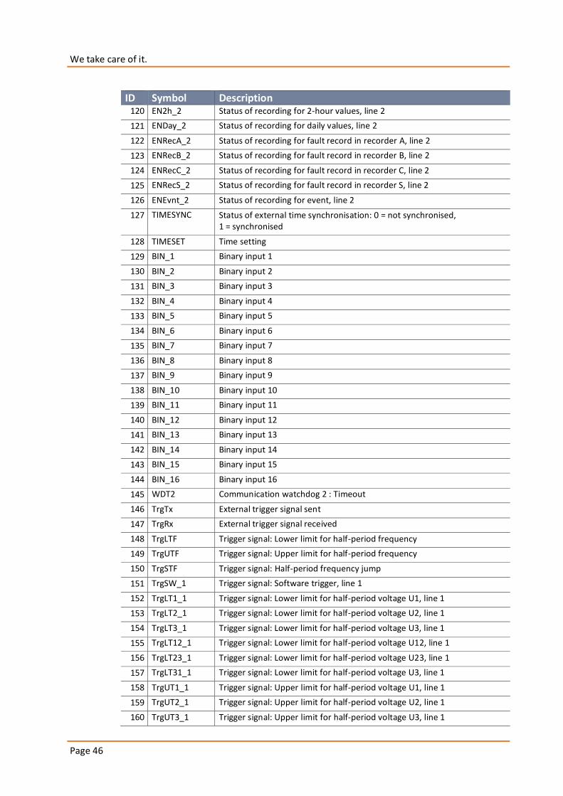
We take care of it.
Page 46
ID Symbol Description 120 EN2h_2 Status of recording for 2-hour values, line 2
121 ENDay_2 Status of recording for daily values, line 2
122 ENRecA_2 Status of recording for fault record in recorder A, line 2
123 ENRecB_2 Status of recording for fault record in recorder B, line 2
124 ENRecC_2 Status of recording for fault record in recorder C, line 2
125 ENRecS_2 Status of recording for fault record in recorder S, line 2
126 ENEvnt_2 Status of recording for event, line 2
127 TIMESYNC Status of external time synchronisation: 0 = not synchronised, 1 = synchronised
128 TIMESET Time setting
129 BIN_1 Binary input 1
130 BIN_2 Binary input 2
131 BIN_3 Binary input 3
132 BIN_4 Binary input 4
133 BIN_5 Binary input 5
134 BIN_6 Binary input 6
135 BIN_7 Binary input 7
136 BIN_8 Binary input 8
137 BIN_9 Binary input 9
138 BIN_10 Binary input 10
139 BIN_11 Binary input 11
140 BIN_12 Binary input 12
141 BIN_13 Binary input 13
142 BIN_14 Binary input 14
143 BIN_15 Binary input 15
144 BIN_16 Binary input 16
145 WDT2 Communication watchdog 2 : Timeout
146 TrgTx External trigger signal sent
147 TrgRx External trigger signal received
148 TrgLTF Trigger signal: Lower limit for half-period frequency
149 TrgUTF Trigger signal: Upper limit for half-period frequency
150 TrgSTF Trigger signal: Half-period frequency jump
151 TrgSW_1 Trigger signal: Software trigger, line 1
152 TrgLT1_1 Trigger signal: Lower limit for half-period voltage U1, line 1
153 TrgLT2_1 Trigger signal: Lower limit for half-period voltage U2, line 1
154 TrgLT3_1 Trigger signal: Lower limit for half-period voltage U3, line 1
155 TrgLT12_1 Trigger signal: Lower limit for half-period voltage U12, line 1
156 TrgLT23_1 Trigger signal: Lower limit for half-period voltage U23, line 1
157 TrgLT31_1 Trigger signal: Lower limit for half-period voltage U3, line 1
158 TrgUT1_1 Trigger signal: Upper limit for half-period voltage U1, line 1
159 TrgUT2_1 Trigger signal: Upper limit for half-period voltage U2, line 1
160 TrgUT3_1 Trigger signal: Upper limit for half-period voltage U3, line 1
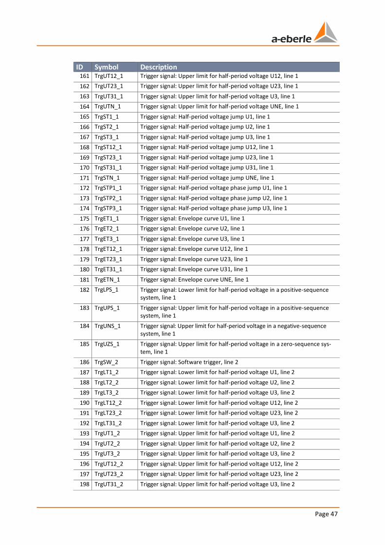
Page 47
ID Symbol Description 161 TrgUT12_1 Trigger signal: Upper limit for half-period voltage U12, line 1
162 TrgUT23_1 Trigger signal: Upper limit for half-period voltage U23, line 1
163 TrgUT31_1 Trigger signal: Upper limit for half-period voltage U3, line 1
164 TrgUTN_1 Trigger signal: Upper limit for half-period voltage UNE, line 1
165 TrgST1_1 Trigger signal: Half-period voltage jump U1, line 1
166 TrgST2_1 Trigger signal: Half-period voltage jump U2, line 1
167 TrgST3_1 Trigger signal: Half-period voltage jump U3, line 1
168 TrgST12_1 Trigger signal: Half-period voltage jump U12, line 1
169 TrgST23_1 Trigger signal: Half-period voltage jump U23, line 1
170 TrgST31_1 Trigger signal: Half-period voltage jump U31, line 1
171 TrgSTN_1 Trigger signal: Half-period voltage jump UNE, line 1
172 TrgSTP1_1 Trigger signal: Half-period voltage phase jump U1, line 1
173 TrgSTP2_1 Trigger signal: Half-period voltage phase jump U2, line 1
174 TrgSTP3_1 Trigger signal: Half-period voltage phase jump U3, line 1
175 TrgET1_1 Trigger signal: Envelope curve U1, line 1
176 TrgET2_1 Trigger signal: Envelope curve U2, line 1
177 TrgET3_1 Trigger signal: Envelope curve U3, line 1
178 TrgET12_1 Trigger signal: Envelope curve U12, line 1
179 TrgET23_1 Trigger signal: Envelope curve U23, line 1
180 TrgET31_1 Trigger signal: Envelope curve U31, line 1
181 TrgETN_1 Trigger signal: Envelope curve UNE, line 1
182 TrgLPS_1 Trigger signal: Lower limit for half-period voltage in a positive-sequence system, line 1
183 TrgUPS_1 Trigger signal: Upper limit for half-period voltage in a positive-sequence system, line 1
184 TrgUNS_1 Trigger signal: Upper limit for half-period voltage in a negative-sequence system, line 1
185 TrgUZS_1 Trigger signal: Upper limit for half-period voltage in a zero-sequence sys-tem, line 1
186 TrgSW_2 Trigger signal: Software trigger, line 2
187 TrgLT1_2 Trigger signal: Lower limit for half-period voltage U1, line 2
188 TrgLT2_2 Trigger signal: Lower limit for half-period voltage U2, line 2
189 TrgLT3_2 Trigger signal: Lower limit for half-period voltage U3, line 2
190 TrgLT12_2 Trigger signal: Lower limit for half-period voltage U12, line 2
191 TrgLT23_2 Trigger signal: Lower limit for half-period voltage U23, line 2
192 TrgLT31_2 Trigger signal: Lower limit for half-period voltage U3, line 2
193 TrgUT1_2 Trigger signal: Upper limit for half-period voltage U1, line 2
194 TrgUT2_2 Trigger signal: Upper limit for half-period voltage U2, line 2
195 TrgUT3_2 Trigger signal: Upper limit for half-period voltage U3, line 2
196 TrgUT12_2 Trigger signal: Upper limit for half-period voltage U12, line 2
197 TrgUT23_2 Trigger signal: Upper limit for half-period voltage U23, line 2
198 TrgUT31_2 Trigger signal: Upper limit for half-period voltage U3, line 2
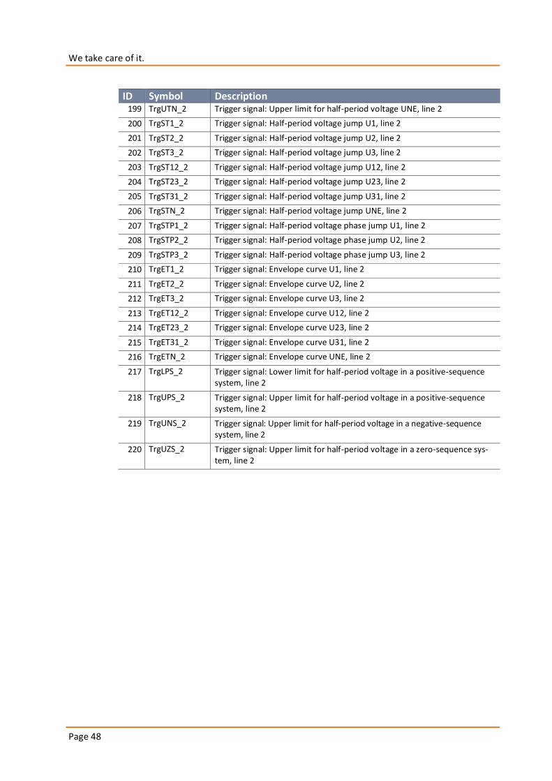
We take care of it.
Page 48
ID Symbol Description 199 TrgUTN_2 Trigger signal: Upper limit for half-period voltage UNE, line 2
200 TrgST1_2 Trigger signal: Half-period voltage jump U1, line 2
201 TrgST2_2 Trigger signal: Half-period voltage jump U2, line 2
202 TrgST3_2 Trigger signal: Half-period voltage jump U3, line 2
203 TrgST12_2 Trigger signal: Half-period voltage jump U12, line 2
204 TrgST23_2 Trigger signal: Half-period voltage jump U23, line 2
205 TrgST31_2 Trigger signal: Half-period voltage jump U31, line 2
206 TrgSTN_2 Trigger signal: Half-period voltage jump UNE, line 2
207 TrgSTP1_2 Trigger signal: Half-period voltage phase jump U1, line 2
208 TrgSTP2_2 Trigger signal: Half-period voltage phase jump U2, line 2
209 TrgSTP3_2 Trigger signal: Half-period voltage phase jump U3, line 2
210 TrgET1_2 Trigger signal: Envelope curve U1, line 2
211 TrgET2_2 Trigger signal: Envelope curve U2, line 2
212 TrgET3_2 Trigger signal: Envelope curve U3, line 2
213 TrgET12_2 Trigger signal: Envelope curve U12, line 2
214 TrgET23_2 Trigger signal: Envelope curve U23, line 2
215 TrgET31_2 Trigger signal: Envelope curve U31, line 2
216 TrgETN_2 Trigger signal: Envelope curve UNE, line 2
217 TrgLPS_2 Trigger signal: Lower limit for half-period voltage in a positive-sequence system, line 2
218 TrgUPS_2 Trigger signal: Upper limit for half-period voltage in a positive-sequence system, line 2
219 TrgUNS_2 Trigger signal: Upper limit for half-period voltage in a negative-sequence system, line 2
220 TrgUZS_2 Trigger signal: Upper limit for half-period voltage in a zero-sequence sys-tem, line 2
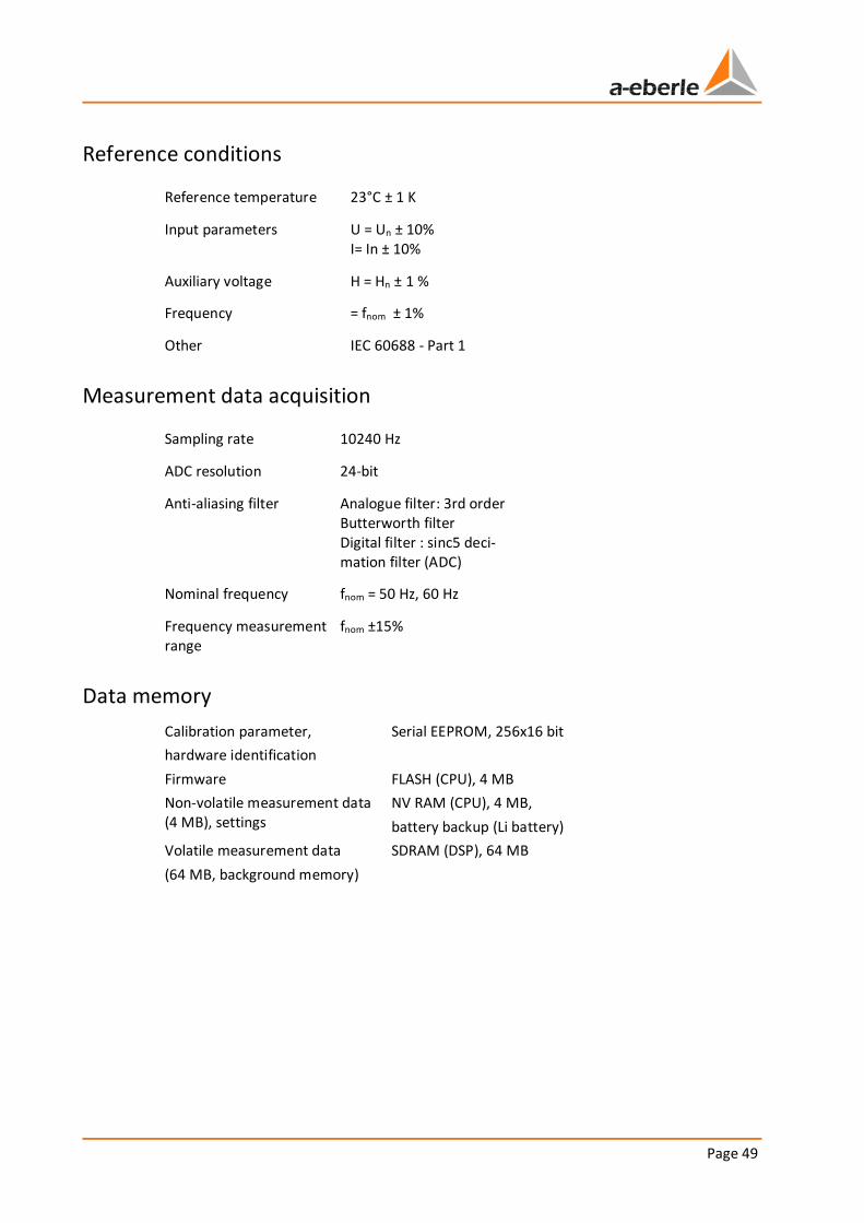
Page 49
Reference conditions
Reference temperature 23°C ± 1 K
Input parameters U = Un ± 10% I= In ± 10%
Auxiliary voltage H = Hn ± 1 %
Frequency = fnom ± 1%
Other IEC 60688 - Part 1
Measurement data acquisition
Sampling rate 10240 Hz
ADC resolution 24-bit
Anti-aliasing filter Analogue filter: 3rd order Butterworth filter Digital filter : sinc5 deci-mation filter (ADC)
Nominal frequency fnom = 50 Hz, 60 Hz
Frequency measurement range
fnom ±15%
Data memory
Calibration parameter,
hardware identification
Serial EEPROM, 256x16 bit
Firmware FLASH (CPU), 4 MB
Non-volatile measurement data (4 MB), settings
NV RAM (CPU), 4 MB,
battery backup (Li battery)
Volatile measurement data
(64 MB, background memory)
SDRAM (DSP), 64 MB
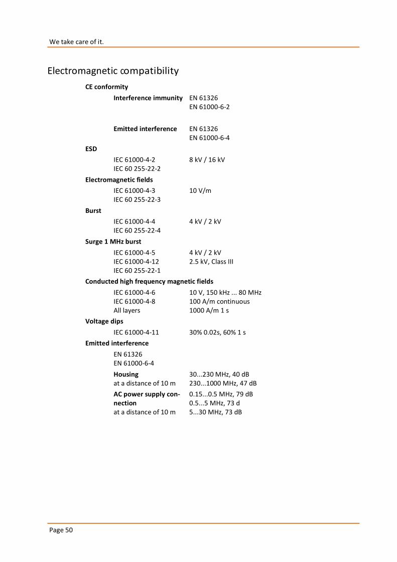
We take care of it.
Page 50
Electromagnetic compatibility
CE conformity
Interference immunity EN 61326 EN 61000-6-2
Emitted interference EN 61326 EN 61000-6-4
ESD
IEC 61000-4-2 IEC 60 255-22-2
8 kV / 16 kV
Electromagnetic fields
IEC 61000-4-3 IEC 60 255-22-3
10 V/m
Burst
IEC 61000-4-4 IEC 60 255-22-4
4 kV / 2 kV
Surge 1 MHz burst
IEC 61000-4-5 IEC 61000-4-12 IEC 60 255-22-1
4 kV / 2 kV 2.5 kV, Class III
Conducted high frequency magnetic fields
IEC 61000-4-6 IEC 61000-4-8 All layers
10 V, 150 kHz ... 80 MHz 100 A/m continuous 1000 A/m 1 s
Voltage dips
IEC 61000-4-11 30% 0.02s, 60% 1 s
Emitted interference
EN 61326 EN 61000-6-4
Housing at a distance of 10 m
30...230 MHz, 40 dB 230...1000 MHz, 47 dB
AC power supply con-nection at a distance of 10 m
0.15...0.5 MHz, 79 dB 0.5...5 MHz, 73 d 5...30 MHz, 73 dB
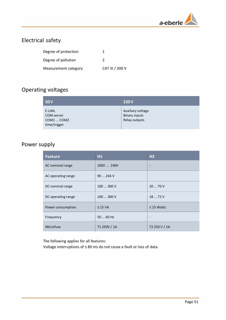
Page 51
Electrical safety
Degree of protection 1
Degree of pollution 2
Measurement category CAT III / 300 V
Operating voltages
50 V 230 V
E-LAN, COM server
COM1 ... COM2 time/trigger
Auxiliary voltage Binary inputs Relay outputs
Power supply
Feature H1 H2
AC nominal range 100V ... 240V -
AC operating range 90 ... 264 V
DC nominal range 100 ... 300 V 20 ... 70 V
DC operating range 100 ... 300 V 18 ... 72 V
Power consumption ≤ 15 VA ≤ 15 Watts
Frequency 50 ... 60 Hz -
Microfuse T1 250V / 1A T2 250 V / 2A
The following applies for all features:
Voltage interruptions of ≤ 80 ms do not cause a fault or loss of data.
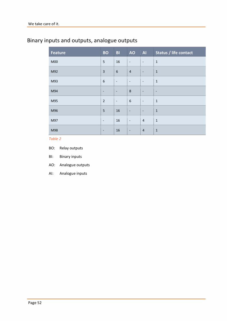
We take care of it.
Page 52
Binary inputs and outputs, analogue outputs
Feature BO BI AO AI Status / life contact
M00 5 16 - - 1
M92 3 6 4 - 1
M93 6 - - - 1
M94 - - 8 - -
M95 2 - 6 - 1
M96 5 16 - - 1
M97 - 16 - 4 1
M98 - 16 - 4 1
Table 2
BO: Relay outputs
BI: Binary inputs
AO: Analogue outputs
AI: Analogue inputs
Page 53
Environmentalconditions
Temperature range
Function Transport and storage
-15 ... +50°C -25 ... +65°C
Humidity
No condensation on 30 days/year
95 % rel.
Dry, cold
IEC 60068-2-1 -15°C / 16 h
Dry, hot
IEC 60068-2-2 +55°C / 16 h
Constant humid heat
IEC 60068-2-3 + 40 °C / 93 % / 2 days
Cyclical humid heat
IEC 60068-2-30 12+12h, 6 cycles, +55°C/93%
Toppling
IEC 60068-2-31 100 mm drop, unwrapped
Vibration
IEC 60255-21-1 Class 1
Impact
IEC 60255-21-2 Class 1
We take care of it.
Page 54
Mechanical design
Plug-in module
Front panel Aluminium, RAL 7035 grey
Height 3 HE (132.5 mm)
Width 18 TE (91.44 mm)
Circuit board 160 mm x 100 mm
Weight ≤ 1.0 kg
Module – degree of protection IP 00
Socket connector - degree of protection
IP 00
Mounting conforms to DIN 41494 Part 5
Plug-in connectors DIN 41612
Housing
The PQI-D is also very flexible with regard to the type of housing used. Some possible types
of housing are described below. The standard versions are the two described at feature B90
and feature B92. Since the number of inputs, outputs, COMs, etc. in a 19" plug-in module is
much greater than the number of available terminals on the housing, pin assignment must
be individually specified for versions B90...B92.
Material Plastic
Degree of protection Housing IP 65
Weight ≤ 1.5 kg
Dimensions See figures 5 and 6
Connection elements Screw terminals
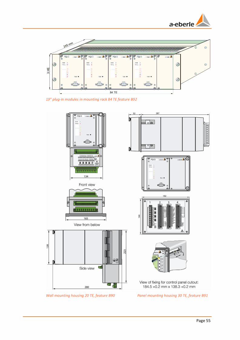
Page 55
19" plug-in modules in mounting rack 84 TE feature B92
Wall mounting housing 20 TE, feature B90 Panel mounting housing 30 TE, feature B91
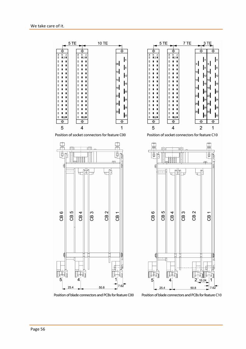
We take care of it.
Page 56
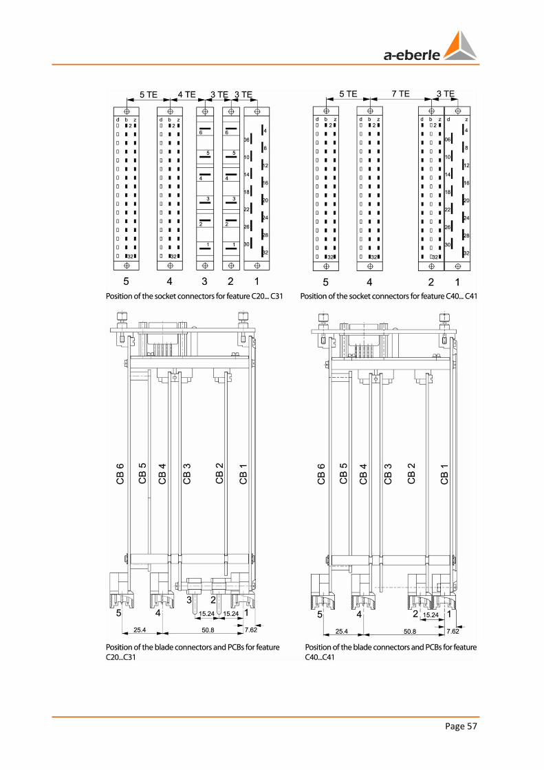
Page 57
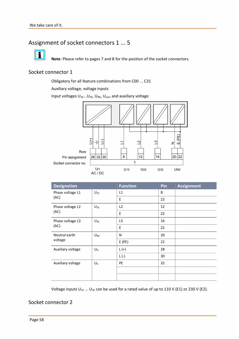
We take care of it.
Page 58
Assignment of socket connectors 1 ... 5
Note: Please refer to pages 7 and 8 for the position of the socket connectors.
Socket connector 1
Obligatory for all feature combinations from C00 ... C31
Auxiliary voltage, voltage inputs
Input voltages U1E...U3E, UNE, Usync and auxiliary voltage
Designation Function Pin Assignment
Phase voltage L1 (AC)
U1E L1 8
E 22
Phase voltage L2 (AC)
U2E L2 12
E 22
Phase voltage L3 (AC)
U3E L3 16
E 22
Neutral earth voltage
UNE N 20
E (PE) 22
Auxiliary voltage UH L (+) 28
L (-) 30
Auxiliary voltage UH PE 32
Voltage inputs U1E ... U3E can be used for a rated value of up to 110 V (E1) or 230 V (E2).
Socket connector 2
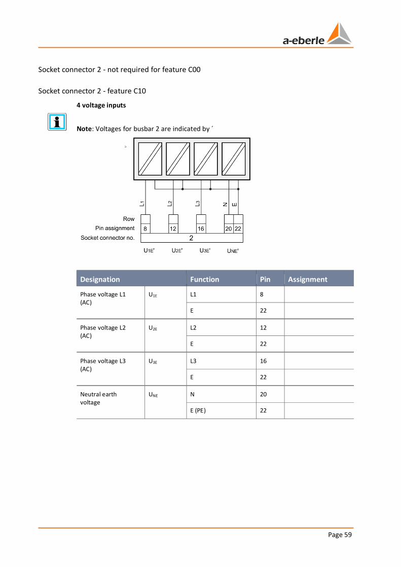
Page 59
Socket connector 2 - not required for feature C00
Socket connector 2 - feature C10
4 voltage inputs
Note: Voltages for busbar 2 are indicated by ´
Designation Function Pin Assignment
Phase voltage L1 (AC)
U1E L1 8
E 22
Phase voltage L2 (AC)
U2E L2 12
E 22
Phase voltage L3 (AC)
U3E L3 16
E 22
Neutral earth voltage
UNE N 20
E (PE) 22
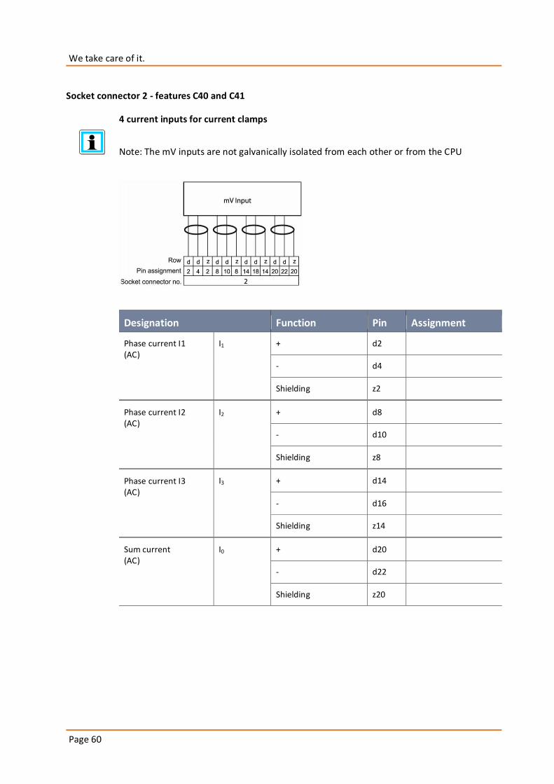
We take care of it.
Page 60
Socket connector 2 - features C40 and C41
4 current inputs for current clamps
Note: The mV inputs are not galvanically isolated from each other or from the CPU
Designation Function Pin Assignment
Phase current I1 (AC)
I1 + d2
- d4
Shielding z2
Phase current I2 (AC)
I2 + d8
- d10
Shielding z8
Phase current I3 (AC)
I3 + d14
- d16
Shielding z14
Sum current (AC)
I0 + d20
- d22
Shielding z20
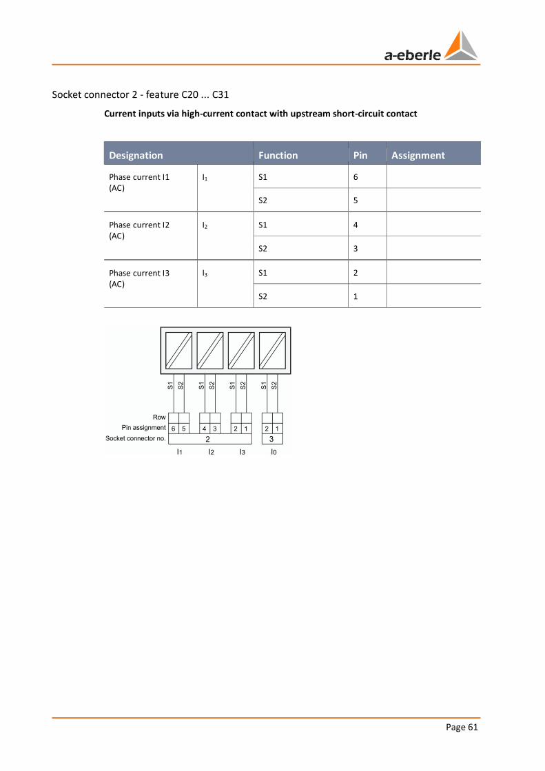
Page 61
Socket connector 2 - feature C20 ... C31
Current inputs via high-current contact with upstream short-circuit contact
Designation Function Pin Assignment
Phase current I1 (AC)
I1 S1 6
S2 5
Phase current I2 (AC)
I2 S1 4
S2 3
Phase current I3 (AC)
I3 S1 2
S2 1
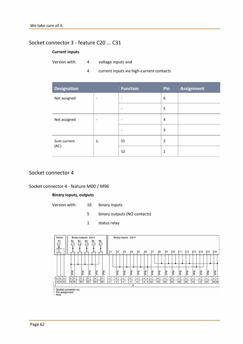
We take care of it.
Page 62
Socket connector 3 - feature C20 ... C31
Current inputs
Version with: 4 voltage inputs and
4 current inputs via high-current contacts
Designation Function Pin Assignment
Not assigned - - 6
- 5
Not assigned - - 4
- 3
Sum current (AC)
I0 S1 2
S2 1
Socket connector 4
Socket connector 4 - feature M00 / M96
Binary inputs, outputs
Version with: 16 binary inputs
5 binary outputs (NO contacts)
1 status relay
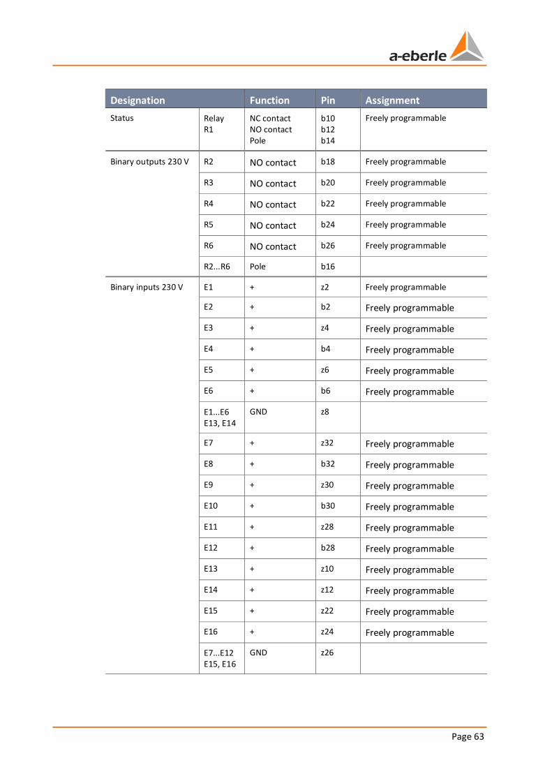
Page 63
Designation Function Pin Assignment
Status Relay R1
NC contact NO contact Pole
b10 b12 b14
Freely programmable
Binary outputs 230 V R2 NO contact b18 Freely programmable
R3 NO contact b20 Freely programmable
R4 NO contact b22 Freely programmable
R5 NO contact b24 Freely programmable
R6 NO contact b26 Freely programmable
R2...R6 Pole b16
Binary inputs 230 V E1 + z2 Freely programmable
E2 + b2 Freely programmable
E3 + z4 Freely programmable
E4 + b4 Freely programmable
E5 + z6 Freely programmable
E6 + b6 Freely programmable
E1...E6 E13, E14
GND z8
E7 + z32 Freely programmable
E8 + b32 Freely programmable
E9 + z30 Freely programmable
E10 + b30 Freely programmable
E11 + z28 Freely programmable
E12 + b28 Freely programmable
E13 + z10 Freely programmable
E14 + z12 Freely programmable
E15 + z22 Freely programmable
E16 + z24 Freely programmable
E7...E12 E15, E16
GND z26
We take care of it.
Page 64
Socket connector 4 - feature M92
Binary inputs, outputs, analogue outputs
Version with: 6 binary inputs
2 binary outputs (NO contacts)
4 analogue outputs
1 status relay
Designation Function Pin Assignment
Analogue outputs K1 + -
z26 b26
Freely programmable
K2 + -
z28 b28
Freely programmable
K3 + -
z30 b30
Freely programmable
K4 + -
z32 b32
Freely programmable
Binary inputs 230 V E1 + z6 Freely programmable
E2 + b6 Freely programmable
E3 + b8 Freely programmable
E1...E3 GND z8
E4 + z2 Freely programmable
E5 + b2 Freely programmable
E6 + b4 Freely programmable
E4...E6 GND z4
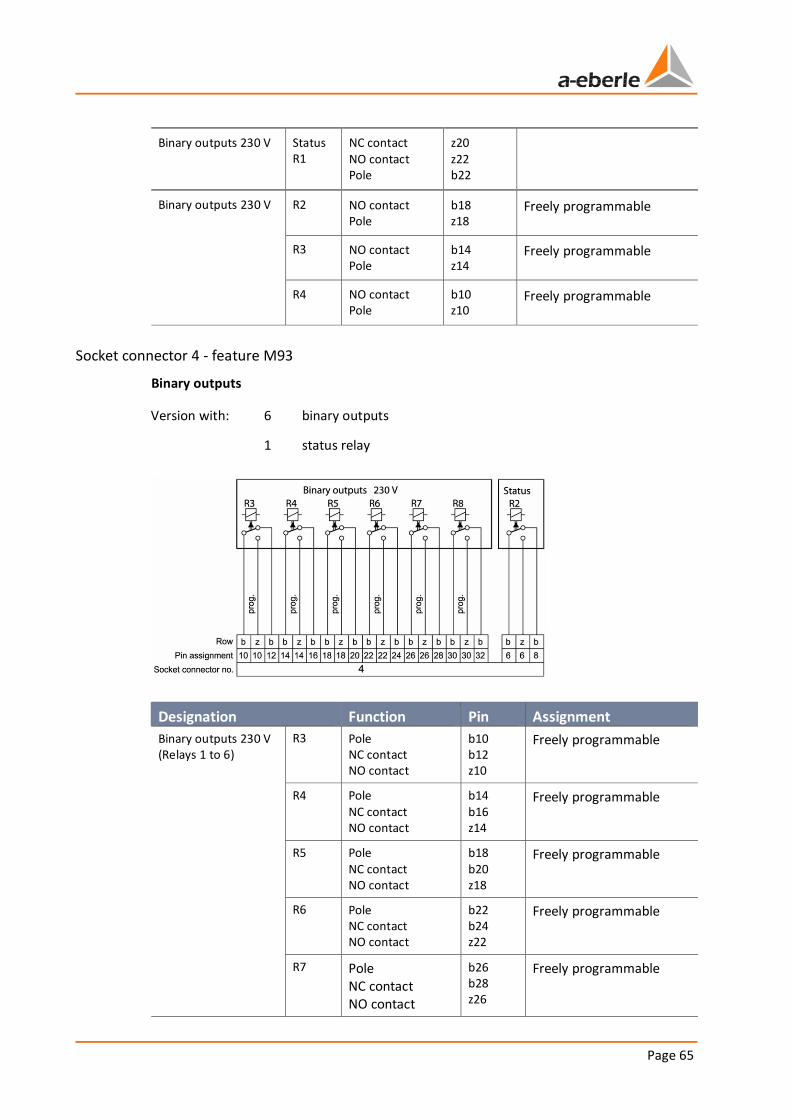
Page 65
Binary outputs 230 V Status R1
NC contact NO contact Pole
z20 z22 b22
Binary outputs 230 V R2 NO contact Pole
b18 z18
Freely programmable
R3 NO contact Pole
b14 z14
Freely programmable
R4 NO contact Pole
b10 z10
Freely programmable
Socket connector 4 - feature M93
Binary outputs
Version with: 6 binary outputs
1 status relay
Designation Function Pin Assignment
Binary outputs 230 V (Relays 1 to 6)
R3 Pole NC contact NO contact
b10 b12 z10
Freely programmable
R4 Pole
NC contact NO contact
b14
b16 z14
Freely programmable
R5 Pole NC contact NO contact
b18 b20 z18
Freely programmable
R6 Pole NC contact NO contact
b22 b24 z22
Freely programmable
R7 Pole NC contact NO contact
b26 b28 z26
Freely programmable
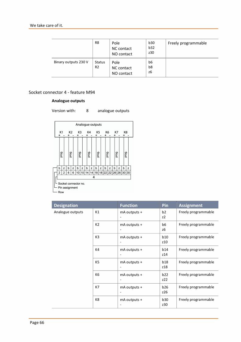
We take care of it.
Page 66
R8 Pole NC contact NO contact
b30 b32 z30
Freely programmable
Binary outputs 230 V Status R2
Pole NC contact NO contact
b6 b8 z6
Socket connector 4 - feature M94
Analogue outputs
Version with: 8 analogue outputs
Designation Function Pin Assignment
Analogue outputs K1 mA outputs + -
b2 z2
Freely programmable
K2 mA outputs + -
b6 z6
Freely programmable
K3 mA outputs + -
b10 z10
Freely programmable
K4 mA outputs + -
b14 z14
Freely programmable
K5 mA outputs + -
b18 z18
Freely programmable
K6 mA outputs + -
b22 z22
Freely programmable
K7 mA outputs + -
b26 z26
Freely programmable
K8 mA outputs + -
b30 z30
Freely programmable
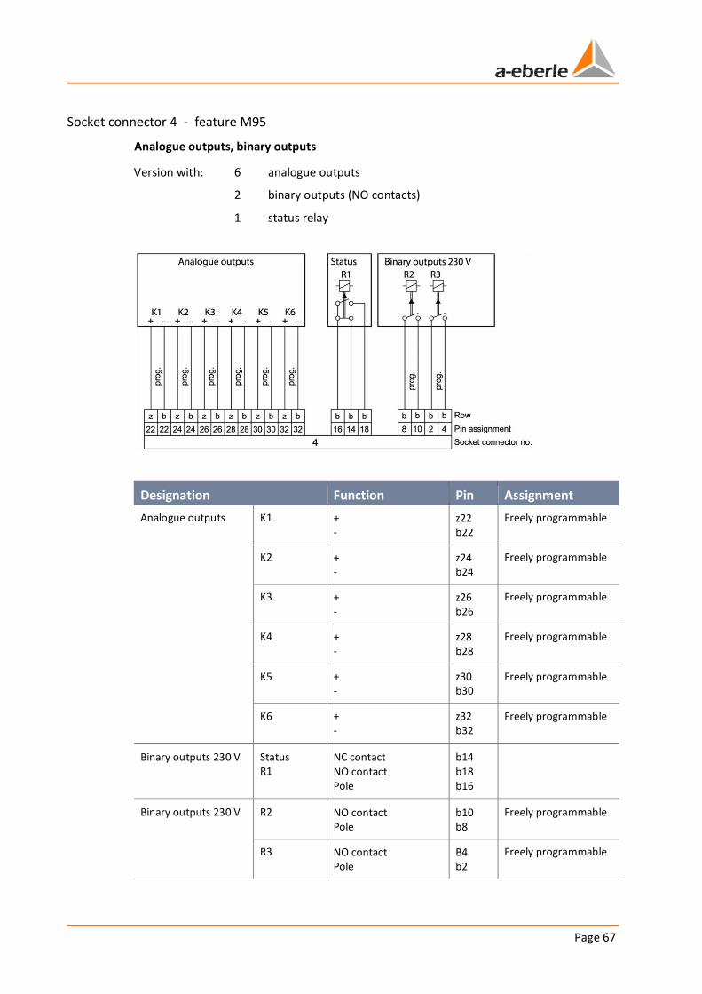
Page 67
Socket connector 4 - feature M95
Analogue outputs, binary outputs
Version with: 6 analogue outputs
2 binary outputs (NO contacts)
1 status relay
Designation Function Pin Assignment
Analogue outputs K1 + -
z22 b22
Freely programmable
K2 + -
z24 b24
Freely programmable
K3 + -
z26 b26
Freely programmable
K4 + -
z28 b28
Freely programmable
K5 + -
z30 b30
Freely programmable
K6 + -
z32 b32
Freely programmable
Binary outputs 230 V Status R1
NC contact NO contact Pole
b14 b18 b16
Binary outputs 230 V R2 NO contact Pole
b10 b8
Freely programmable
R3 NO contact Pole
B4 b2
Freely programmable
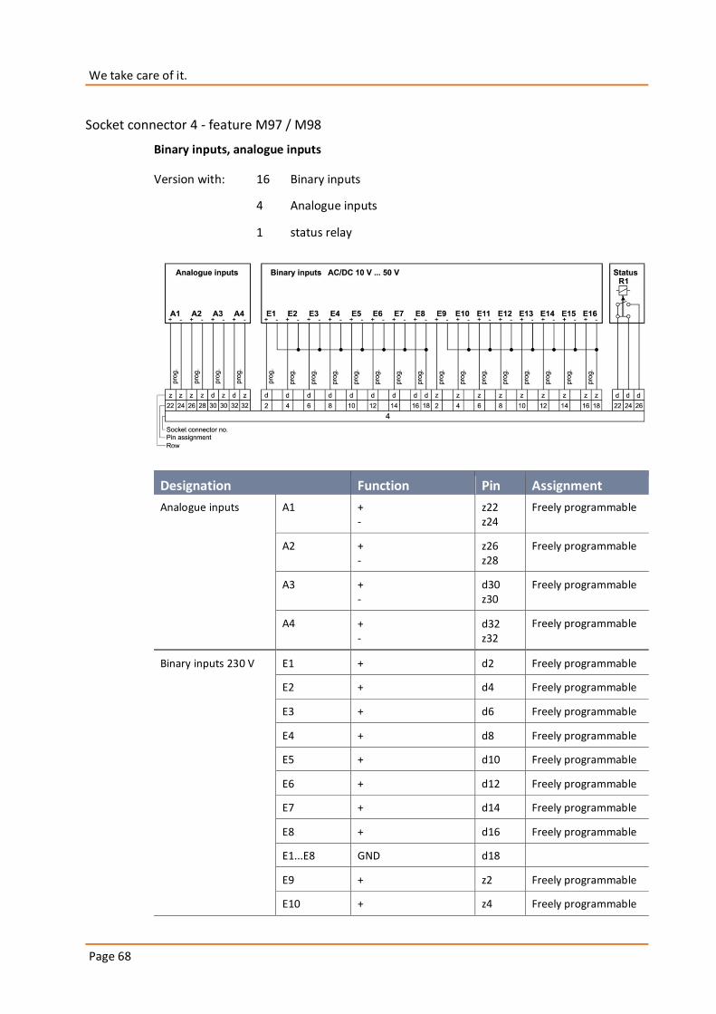
We take care of it.
Page 68
Socket connector 4 - feature M97 / M98
Binary inputs, analogue inputs
Version with: 16 Binary inputs
4 Analogue inputs
1 status relay
Designation Function Pin Assignment
Analogue inputs A1 + -
z22 z24
Freely programmable
A2 + -
z26 z28
Freely programmable
A3 + -
d30 z30
Freely programmable
A4 + -
d32 z32
Freely programmable
Binary inputs 230 V E1 + d2 Freely programmable
E2 + d4 Freely programmable
E3 + d6 Freely programmable
E4 + d8 Freely programmable
E5 + d10 Freely programmable
E6 + d12 Freely programmable
E7 + d14 Freely programmable
E8 + d16 Freely programmable
E1...E8 GND d18
E9 + z2 Freely programmable
E10 + z4 Freely programmable
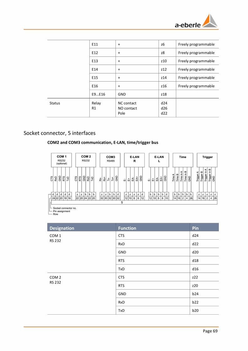
Page 69
E11 + z6 Freely programmable
E12 + z8 Freely programmable
E13 + z10 Freely programmable
E14 + z12 Freely programmable
E15 + z14 Freely programmable
E16 + z16 Freely programmable
E9...E16 GND z18
Status Relay R1
NC contact
NO contact Pole
d24
d26 d22
Socket connector, 5 interfaces
COM2 and COM3 communication, E-LAN, time/trigger bus
Designation Function Pin
COM 1 RS 232
CTS d24
RxD d22
GND d20
RTS d18
TxD d16
COM 2 RS 232
CTS z22
RTS z20
GND b24
RxD b22
TxD b20
We take care of it.
Page 70
COM 3 RS 485
Rx - z32
Rx + z30
Tx - b32
Tx + b30
GND d32
E-LAN R (right) E- z12
E+ z10
EA- z8
EA+ z6
GND d12
E-LAN L (left) E- b12
E+ b10
EA- b8
EA+ b6
GND d10
Time Time A b14
Time B b16
Time in A b2
Time in B b4
GND b26
Trigger Trigger A z14
Trigger B z16
Trigger in A z2
Trigger in B z4
GND z26
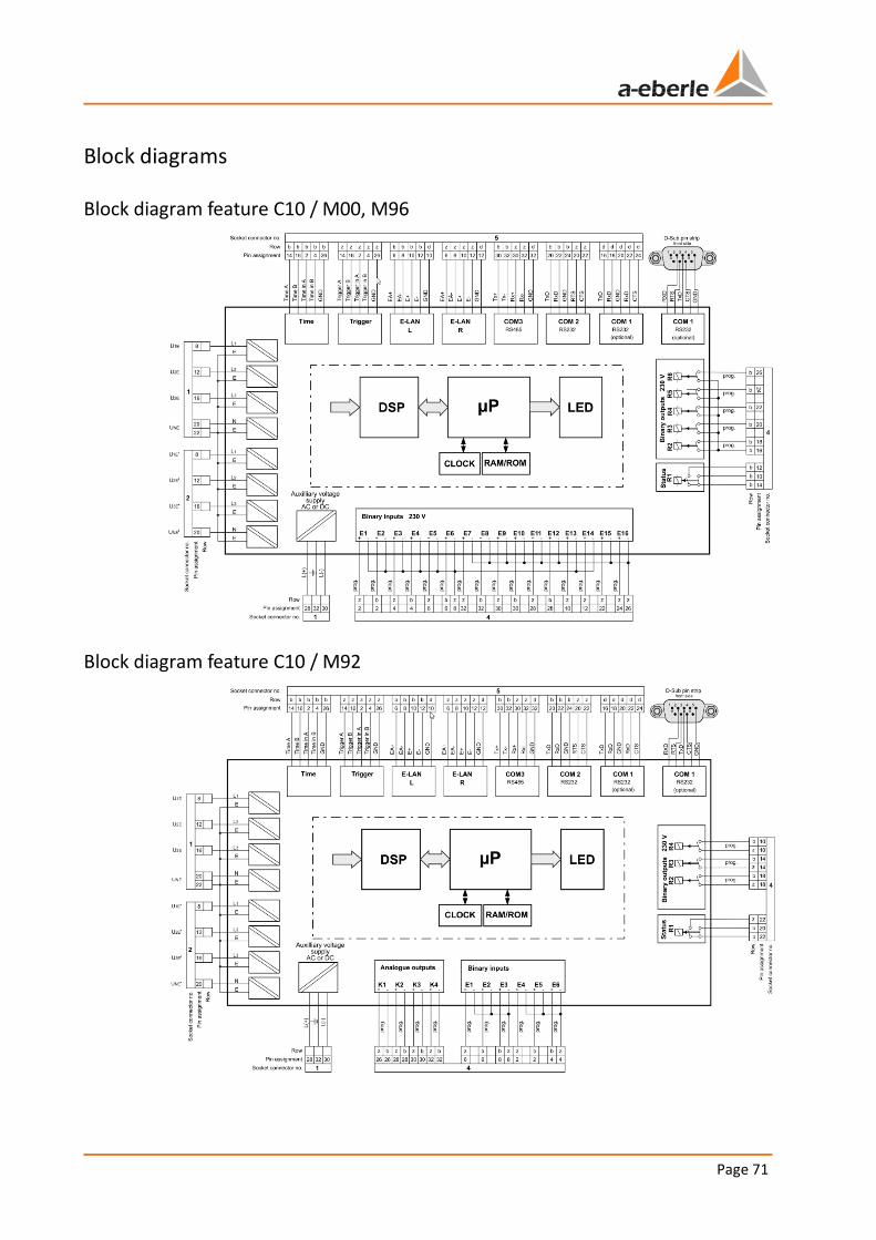
Page 71
Block diagrams
Block diagram feature C10 / M00, M96
Block diagram feature C10 / M92
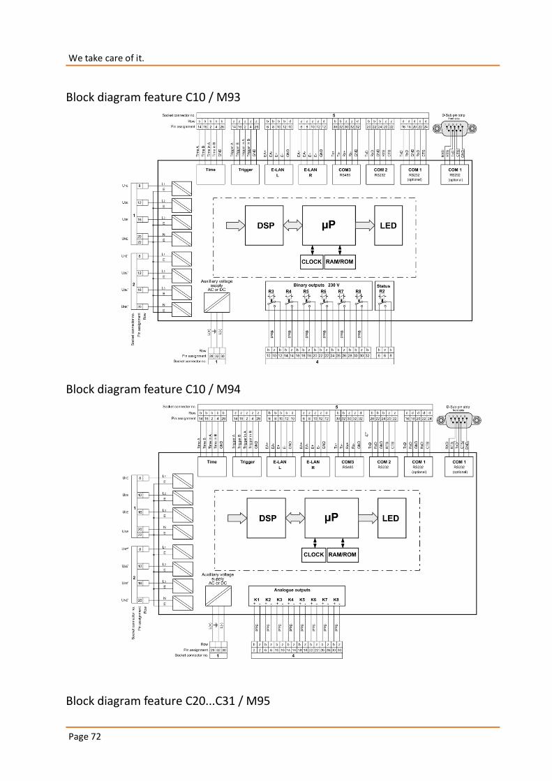
We take care of it.
Page 72
Block diagram feature C10 / M93
Block diagram feature C10 / M94
Block diagram feature C20...C31 / M95
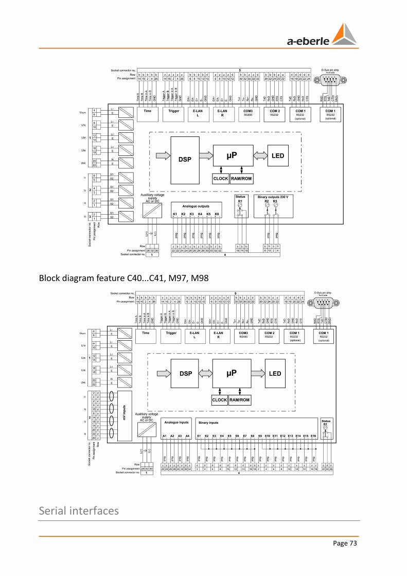
Page 73
Block diagram feature C40...C41, M97, M98
Serial interfaces
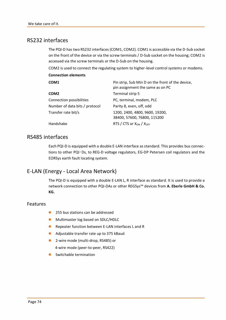
We take care of it.
Page 74
RS232 interfaces
The PQI-D has two RS232 interfaces (COM1, COM2). COM1 is accessible via the D-Sub socket
on the front of the device or via the screw terminals / D-Sub socket on the housing; COM2 is
accessed via the screw terminals or the D-Sub on the housing.
COM2 is used to connect the regulating system to higher-level control systems or modems.
Connection elements
COM1 Pin strip, Sub Min D on the front of the device, pin assignment the same as on PC
COM2 Terminal strip 5
Connection possibilities PC, terminal, modem, PLC
Number of data bits / protocol Parity 8, even, off, odd
Transfer rate bit/s 1200, 2400, 4800, 9600, 19200, 38400, 57600, 76800, 115200
Handshake RTS / CTS or XON / XOFF
RS485 interfaces
Each PQI-D is equipped with a double E-LAN interface as standard. This provides bus connec-
tions to other PQI‑Ds, to REG-D voltage regulators, EG-DP Petersen coil regulators and the
EORSys earth fault locating system.
E-LAN (Energy - Local Area Network)
The PQI-D is equipped with a double E-LAN L, R interface as standard. It is used to provide a
network connection to other PQI-DAs or other REGSys™ devices from A. Eberle GmbH & Co.
KG.
Features
0 255 bus stations can be addressed
0 Multimaster log based on SDLC/HDLC
0 Repeater function between E-LAN interfaces L and R
0 Adjustable transfer rate up to 375 kBaud
0 2-wire mode (multi-drop, RS485) or
4-wire mode (peer-to-peer, RS422)
0 Switchable termination
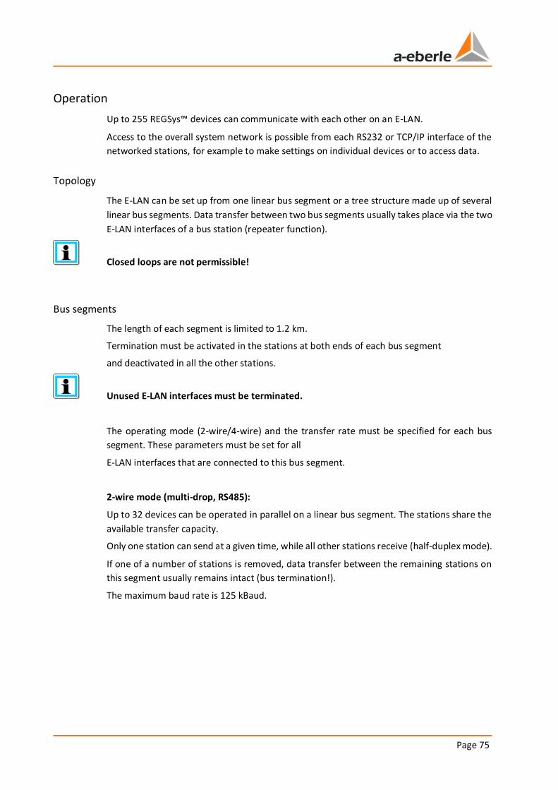
Page 75
Operation
Up to 255 REGSys™ devices can communicate with each other on an E-LAN.
Access to the overall system network is possible from each RS232 or TCP/IP interface of the
networked stations, for example to make settings on individual devices or to access data.
Topology
The E-LAN can be set up from one linear bus segment or a tree structure made up of several
linear bus segments. Data transfer between two bus segments usually takes place via the two
E-LAN interfaces of a bus station (repeater function).
Closed loops are not permissible!
Bus segments
The length of each segment is limited to 1.2 km.
Termination must be activated in the stations at both ends of each bus segment
and deactivated in all the other stations.
Unused E-LAN interfaces must be terminated.
The operating mode (2-wire/4-wire) and the transfer rate must be specified for each bus
segment. These parameters must be set for all
E-LAN interfaces that are connected to this bus segment.
2-wire mode (multi-drop, RS485):
Up to 32 devices can be operated in parallel on a linear bus segment. The stations share the
available transfer capacity.
Only one station can send at a given time, while all other stations receive (half-duplex mode).
If one of a number of stations is removed, data transfer between the remaining stations on
this segment usually remains intact (bus termination!).
The maximum baud rate is 125 kBaud.
We take care of it.
Page 76
4-wire mode (peer-to-peer, RS422):
2 devices are connected via one segment; the wire pairs for
sending and receiving must be crossed in this mode.
Both devices have the full transfer capacity and can send simultaneously (full-duplex mode).
If a station is removed, data transfer is interrupted.
The maximum baud rate is 375 kBaud.
Converter - booster
If distances of > 1.2 km are spanned, or if existing transmission lengths are to be used, a bus
segment can be set up in 4-wire mode with the two interconnected bus converters (e.g.
RS422<->optical fibre) of the transmission length.
Bus IDs
Each E-LAN station must be assigned a unique address
(A...A9, B...B9, C...C9.....Z...Z4).
System planning
Topology planning becomes more and more important as the data quantity to be transferred
and the number of stations increase and as the expected response times of the system de-
crease.
Please note that all stations that are connected to a bus segment or to be accessed
via an RS232 or TCP/IP interface share the transfer capacity of the respective data channel.
Which data quantity of which devices is accessed at which devices is an important consider-
ation. The data quantity to be accessed via one interface should be restricted.
The maximum amount of data on one bus segment should not exceed the transfer capacity.
In this regard, 4-wire mode is superior to 2-wire mode.
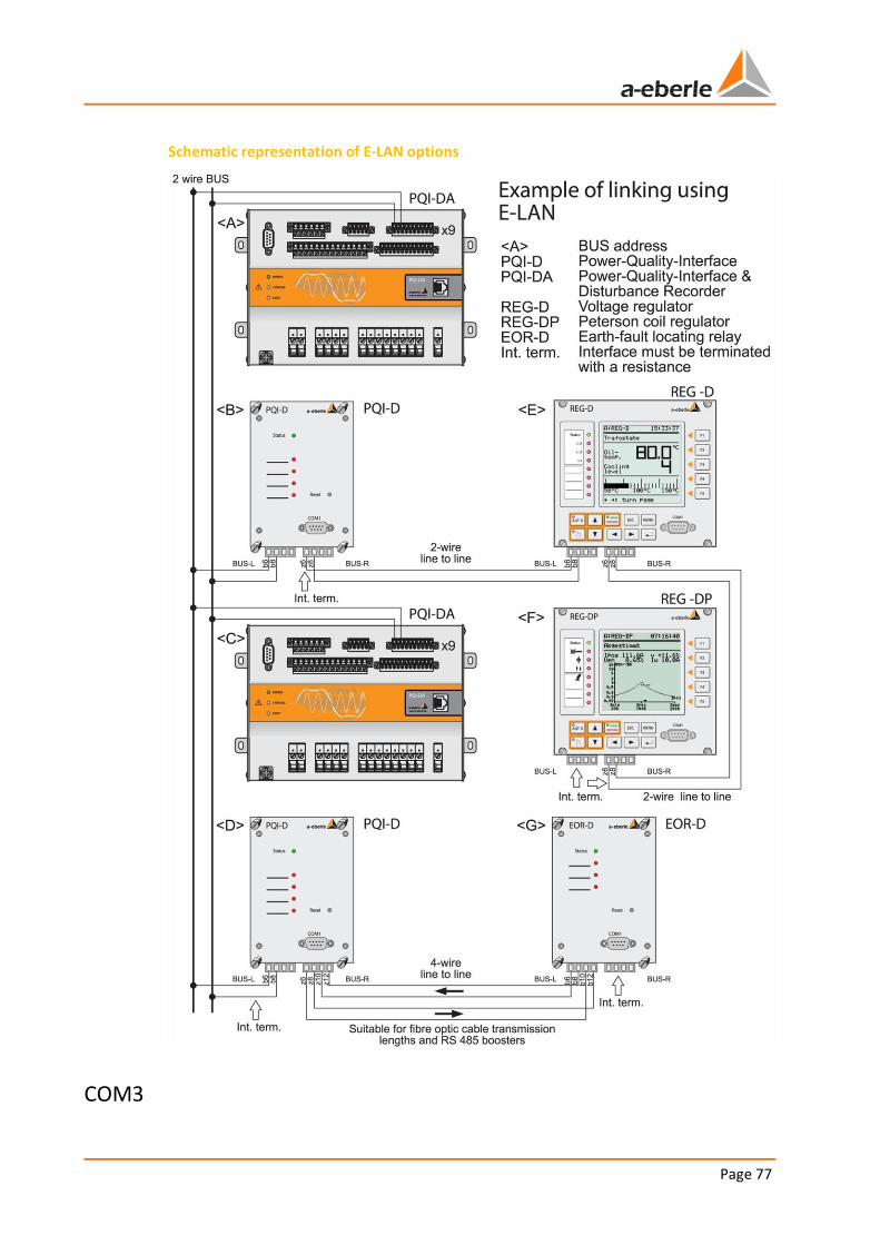
Page 77
Schematic representation of E-LAN options
COM3
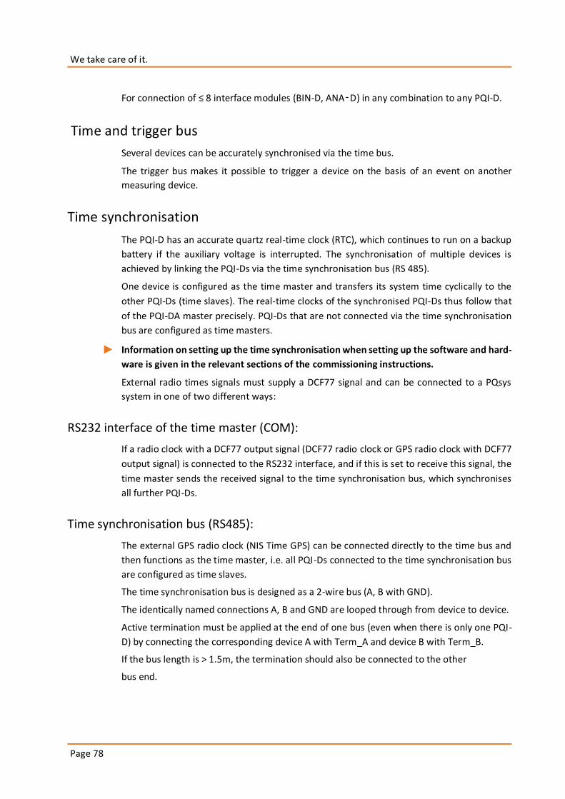
We take care of it.
Page 78
For connection of ≤ 8 interface modules (BIN-D, ANA‑D) in any combination to any PQI-D.
Time and trigger bus
Several devices can be accurately synchronised via the time bus.
The trigger bus makes it possible to trigger a device on the basis of an event on another
measuring device.
Time synchronisation
The PQI-D has an accurate quartz real-time clock (RTC), which continues to run on a backup
battery if the auxiliary voltage is interrupted. The synchronisation of multiple devices is
achieved by linking the PQI-Ds via the time synchronisation bus (RS 485).
One device is configured as the time master and transfers its system time cyclically to the
other PQI-Ds (time slaves). The real-time clocks of the synchronised PQI-Ds thus follow that
of the PQI-DA master precisely. PQI-Ds that are not connected via the time synchronisation
bus are configured as time masters.
1 Information on setting up the time synchronisation when setting up the software and hard-
ware is given in the relevant sections of the commissioning instructions.
External radio times signals must supply a DCF77 signal and can be connected to a PQsys
system in one of two different ways:
RS232 interface of the time master (COM):
If a radio clock with a DCF77 output signal (DCF77 radio clock or GPS radio clock with DCF77
output signal) is connected to the RS232 interface, and if this is set to receive this signal, the
time master sends the received signal to the time synchronisation bus, which synchronises
all further PQI-Ds.
Time synchronisation bus (RS485):
The external GPS radio clock (NIS Time GPS) can be connected directly to the time bus and
then functions as the time master, i.e. all PQI-Ds connected to the time synchronisation bus
are configured as time slaves.
The time synchronisation bus is designed as a 2-wire bus (A, B with GND).
The identically named connections A, B and GND are looped through from device to device.
Active termination must be applied at the end of one bus (even when there is only one PQI-
D) by connecting the corresponding device A with Term_A and device B with Term_B.
If the bus length is > 1.5m, the termination should also be connected to the other
bus end.
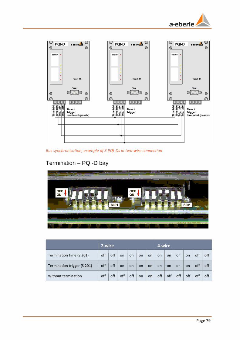
Page 79
Bus synchronisation, example of 3 PQI-Ds in two-wire connection
Termination – PQI-D bay
2-wire 4-wire
Termination time (S 301) off off on on on on on on on on off off
Termination trigger (S 201) off off on on on on on on on on off off
Without termination off off off off on on off off off off off off
We take care of it.
Page 80
External trigger
The PQI-D can record fault records triggered by events. If several devices are interconnected
via the trigger bus, each PQI-D can send a pulse that triggers simultaneous recording of fault
records on the other bus stations when a trigger event occurs. This function can be acti-
vated/deactivated during setup.
The external trigger should always be activated if the exact time sequence of events is re-
quired.
The maximum length of a bus segment is 1.2 km in accordance with RS 485 standard; up to
32 devices can be connected. If the trigger bus is restricted to such a segment (within one
wire), a 2-wire configuration (A, B and GND) is sufficient: At each device, RxA is connected to
TxA and RxB to TxB.
The identically named connections RxA, RxB and GND are looped through from device to
device.
Active termination must be applied at one end of the bus.
If the bus cable length is > 1.5m, termination of the PQI-D should also be connected at the
other end of the bus.
If the trigger bus is made up of several segments that are connected via converters (e.g. FO
star couplers), 4-wire operation (RxA, RxB, TxA, TxB with GND) is necessary:
The identically named connections xA, RxB, TxA, TxB and GND are looped through from de-
vice to device in each bus segment and connected to the corresponding
signals of the converter at one end of the bus (Rx->TxD, Tx->RxD).
The Tx bus must be terminated actively at the first PQI-D.
Page 81
Voltage quality monitor
Standard analysis
Sources: EN 50160, IEC 61000-4-30
1 Supply voltage (EN 50160):
R.m.s. value of the voltage at the transfer point
1 Agreed supply voltage Uc (EN 50160):
Nominal voltage, unless an alternative is agreed upon between the power supply company
and the customer.
1 Normal operating conditions (EN 50160):
Describes the operating status in a distribution network in which current supply require-
ments are met, switching operations are carried out and faults are rectified using automatic
protection systems without any unusual circumstances arising due to external influences or
large bottlenecks in the supply.
1 Slow voltage change (EN 50160):
Changes in the r.m.s. value of the voltage due to changes in the load.
1 Fast voltage change (EN 50160):
An individual fast change in the r.m.s. value of the voltage between two successive voltage
levels that each have a definite but non-specific length (DIN EN 61000-3-3, DIN EN 61000-4-
15).
1 Flicker (EN 50160):
This describes fluctuations in the supply voltage which cause the visual brightness of an at-
tached lamp to change by a certain amount.
Short-term flicker magnitude Pst: 10-minute interval value
Long-term flicker magnitude Pst: 2-hour average value of 12 Pst values
1 Voltage dip (EN 50160):
Drop in the r.m.s. value of the voltage to 90%..1% of Uc.
1 Planned/random voltage interruption (EN 50160):
R.m.s. value of the voltage < 1% of Uc.
Duration 3 minutes: Long-term interruption
< 3 min: Short-term interruption
1 Intermittent overvoltage at the network frequency (EN 50160) :
R.m.s value of the voltage increases to > 170% of Uc.
1 nth order harmonic voltage :
Spectral components with a frequency n times the basic frequency of a periodic voltage.
1 THD (= Total Harmonic Distortion) :
We take care of it.
Page 82
R.m.s. value of harmonic voltages n=2..40 based on the r.m.s. value of the fundamental os-
cillation.
1 Network signal transfer voltage (EN 50160):
R.m.s. value [%] of the ripple control signals of the audio frequency (110 Hz..3 kHz) or car-
rier frequency signals (3…148.5 kHz) based on Uc.
1 Voltage asymmetry:
The degree to which the voltage vectors of the the fundamental oscillation differ from the
symmetrical state of the 3-phase network (two successive phases having the same amplitude
and phase difference) is measured using the relationship between the positive-system and
negative-system components.
1 Voltage dip (IEC 61000-4-30) :
Temporary drop in the voltage at a point in the electrical system below a threshold. An inter-
ruption is a special case of a voltage dip. Minimum voltage and the duration are essential
characteristic values.
1 Voltage Swell (IEC 61000-4-30) :
Temporary increase in the voltage at a point in the electrical system above a threshold. Max-
imum voltage and the duration are important characteristic values.
Overview EN50160 (2010)
Characteristics of the voltage supply
Values / ranges of values
Measurement and evaluation pa-rameters
Low voltage
Medium voltage
Bas
ic q
uan
tity
Inte
grat
ion
in-
terv
al
Mo
nit
ori
ng
pe-
rio
d
Req
uir
ed p
er-
cen
tage
Frequency (when con-nected to an integrated network)
49.5 Hz to 50.5 Hz
47 Hz to 52 Hz
Average va-lue
10 s 1 year 99,5% 100%
Slow voltage change 230 V
+10% / -10%
Uc
+10% / -10%
R.m.s. value 10 min
1 week
95% LV
99% MV
Fast voltage change 5% 4% R.m.s. value 10 ms 1 day 100%
Flicker (specification only for long-term flicker)
P = 1 Flicker algo-rithm
2 h 1 week 95%
Voltage dips (< 1 min)
Tens to 1000 per year (under 85% Uc)
R.m.s. value 10 ms 1 year 100%
Short interruption to the supply (< 3 min)
Tens to several hundred per year
R.m.s. value 10 ms 1 year 100%
Page 83
Random long interruptions to the supply (>3 min)
Tens to 50 per year (under 1% Uc)
R.m.s. value 10 ms 1 year 100%
Intermittent overvoltage at
the network frequency (ex-ternal conductor - earth)
Nor-
mally < 1.5 kV
1.7 to 2.0 Uc (dependent
on neutral point connec-tion)
R.m.s. value 10 ms None 100%
Transient overvoltage (external conductor - earth)
Nor-mally < 6 kV
depending on isolation coor-dination
Peak value None None 100%
Voltage asymmetry (ratio of
negative-sequence system to positive-sequence sys-tem)
Normally 2 % Up to 3 % in special cases
R.m.s. value 10 min
1 week 95%
Harmonic voltage (reference value Un or Uc)
Total harmonic distortion (THD) = 8 %
R.m.s. value 10 min
1 week 95%
Interharmonic voltage Values not yet available Values not yet available
Signal voltages (reference value Un or Uc)
(MV: 9 to 95 kHz range not yet available)
R.m.s. value 3 s 1 day 99%
Characteristics of the voltage supply
Feature: Interruption to the supply
0 Measurement quantities: Half-period r.m.s. voltage values
0 Parameters: Threshold (EN 50160) = 0.01*UC
Maximum length of short interruptions to the supply (EN 50160) = 180 s
0 Statistical quantities: Number and duration
Short interruptions to the supply :
Number per day, week and year
Integration over days, weeks and years
Long interruptions to the supply:
Number per day, week and year
Integration over days, weeks and years
0 Reference values for number per year according to EN 50160:
Short interruption to supply: “Tens to several hundred”, default value = 30
Long interruption to supply: “Fewer than 10 to 50”, default value = 10
We take care of it.
Page 84
Feature: Slow voltage change
0 Event: 10-minute interval with range exceeded
0 Measurement quantities: 10-minute average values of the r.m.s. voltage values
0 Parameters :
Thresholds (EN 50160) = (1 ±0.1)*UC
Default value of lower threshold: 0.9*UC
Default value of upper threshold: 1.1*UC
0 Statistical quantities:
Number per day, week and year
0 Max. relative frequency at each weekly interval
according to EN 50160: 5%
Default value: 5%
Feature: Voltage dip
0 Measurement quantities: Half-period r.m.s. voltage values
0 Parameter:
Threshold (EN 50160) = 0.01..0.90*UC, fefault value = 0.90*UC
0 Statistical quantities: Number and duration
Number per day, week and year
Integration over days, weeks and years
0 Reference value for number per year according to EN 51060:
"Tens to 1000", default value = 100
Feature: Intermittent overvoltage at the network frequency between the outer conductor
and earth
0 Measurement quantities: Half-period r.m.s. voltage values
0 Parameters: Threshold (EN 50160) = 1.7..2.0*UC, default value = 1.7*UC
0 Statistical quantities: Number and duration
Number per day, week and year
Integration over days, weeks and years
0 Reference value for number per year according to EN 50160: None
default value = 10
Feature: Fast voltage change
0 Measurement quantities: Half-period r.m.s. voltage values
0 Parameter:
Threshold (EN 50160) = ±0.04..0.06*UC
default threshold value = 0.06*UC
Minimum duration of stationary status, default value = 1 s
0 Statistical quantities: Number and duration
Number per day, week and year
Integration over days, weeks and years
Page 85
0 Reference value for number per day according to EN 51060:
"Several possible", default = 10
Number per year: Default value = 3650
Feature: Voltage asymmetry
0 Event: 10-minute interval with range exceeded
0 Measurement quantities: 10-minute average value for voltage asymmetry
0 Parameters: Threshold (EN 50160) = 2..3%
Default value: 2%
0 Statistical quantities: Number per day, week and year
0 Max. relative frequency at each weekly interval according to EN 50160: 5%
Default value: 5%
Feature: Harmonic voltages, THD
0 Event: 10-minute interval, range of at least one harmonic voltage or the THD is ex-
ceeded.
0 Measurement quantities: 10-minute average values of harmonic voltages (r.m.s.), THD
0 Parameters :
Thresholds (EN 50160) = harmonic: See table 2 in EN 50160 THD: 8%
Default value: According to EN 50160
0 Statistical quantities: Number per day, week and year
0 Max. relative frequency at each weekly interval according to EN 50160: 5%
Default value: 5%
Feature: Network signal transfer voltages
0 Measurement quantities: 3-second average values of network signal transfer voltages
(%)
0 Parameter:
Thresholds (EN 50160) = see Figures 1 and 2 in EN 50160
Carrier frequency
Default value: Carrier frequency = 168 Hz, threshold = 9 %
0 Statistical quantities: Number and duration
Number per day, week and year
Integration over days, weeks and years
0 Max. relative frequency at each daily interval according to EN 50160: 1%
Default value: 1%
We take care of it.
Page 86
Feature: Flicker
0 Event: 2-hour interval with range exceeded
0 Measurement quantities: Long-term flicker magnitude Plt (2-hour average value)
0 Parameters: Threshold (EN 50160) = 1.0
Default value: 1.0
0 Statistical quantities: Number per day, week and year
0 Max. relative frequency at each weekly interval according to EN 50160: 5%
Default value: 5%
Feature: Network frequency, narrow range
0 Measurement quantities: 10-second average value
0 Parameter:
Thresholds (EN 50160, synchronised connection to the integrated network) = 50 Hz, ±
0.5 Hz
Default value of lower threshold = 49.5 Hz
Default value of upper threshold = 50.5 Hz
0 Statistical quantities: Number and duration
Number per day, week and year
Integration over days, weeks and years
0 Reference value for relative frequency per year according to EN 50160: 0.5%
Default value: 0.5%
Feature: Network frequency, wide range
0 Measurement quantities: 10-second average value
0 Parameters:
Thresholds (EN 50160, synchronised connection to the integrated network) = 47 Hz, 52
Hz
Default value of lower threshold = 47.0 Hz
Default value of upper threshold = 52.0 Hz
0 Statistical quantities: Number and duration
Number per day, week and year
Integration over days, weeks and years
0 Reference value for relative frequency according to EN 50160: 0%
Default value: 0%
Page 87
Network quality events
.The features of the supply voltage are measured in the corresponding aggregation intervals
and monitored with the (adjustable) network quality tolerance thresholds.
If the tolerance ranges are violated, network quality events are produced, recorded, and their
duration and frequency accumulated at certain intervals.
The data acquired in this way are so compact that they can be recorded autonomously over
longer periods. Event processing is a multi-level procedure that comprises the production,
evaluation and recording of events.
In 3-conductor systems, only the voltage between the outer conductors are monitored
according to EN50160.
In 4-conductor systems, the voltages between the outer conductors and the neutral conduc-
tor are also monitored. Limit value monitoring is carried out with hysteresis (exception: fast
voltage change)
The events are first generated separately for each of the phase voltages being monitored
("phase events").
There are two basic types for aggregation of events over time
Interval events
Start/stop events
Evaluation of the network quality is based on network events that are produced by combining
the phase events of a feature.
Depending on the type, events can be represented as one or several event entries with the
same format:
Time stamp : time at which the event was triggered
Identifier : indicates type
Event value : dependent on the type of event
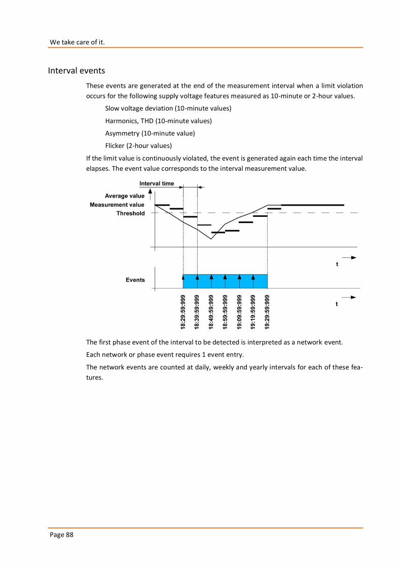
We take care of it.
Page 88
Interval events
These events are generated at the end of the measurement interval when a limit violation
occurs for the following supply voltage features measured as 10-minute or 2-hour values.
Slow voltage deviation (10-minute values)
Harmonics, THD (10-minute values)
Asymmetry (10-minute value)
Flicker (2-hour values)
If the limit value is continuously violated, the event is generated again each time the interval
elapses. The event value corresponds to the interval measurement value.
The first phase event of the interval to be detected is interpreted as a network event.
Each network or phase event requires 1 event entry.
The network events are counted at daily, weekly and yearly intervals for each of these fea-
tures.
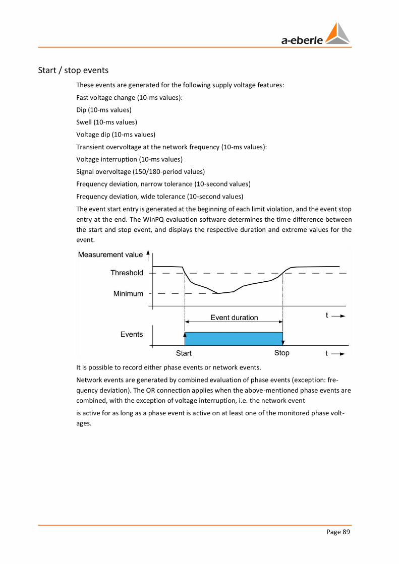
Page 89
Start / stop events
These events are generated for the following supply voltage features:
Fast voltage change (10-ms values):
Dip (10-ms values)
Swell (10-ms values)
Voltage dip (10-ms values)
Transient overvoltage at the network frequency (10-ms values):
Voltage interruption (10-ms values)
Signal overvoltage (150/180-period values)
Frequency deviation, narrow tolerance (10-second values)
Frequency deviation, wide tolerance (10-second values)
The event start entry is generated at the beginning of each limit violation, and the event stop
entry at the end. The WinPQ evaluation software determines the time difference between
the start and stop event, and displays the respective duration and extreme values for the
event.
It is possible to record either phase events or network events.
Network events are generated by combined evaluation of phase events (exception: fre-
quency deviation). The OR connection applies when the above-mentioned phase events are
combined, with the exception of voltage interruption, i.e. the network event
is active for as long as a phase event is active on at least one of the monitored phase volt-
ages.
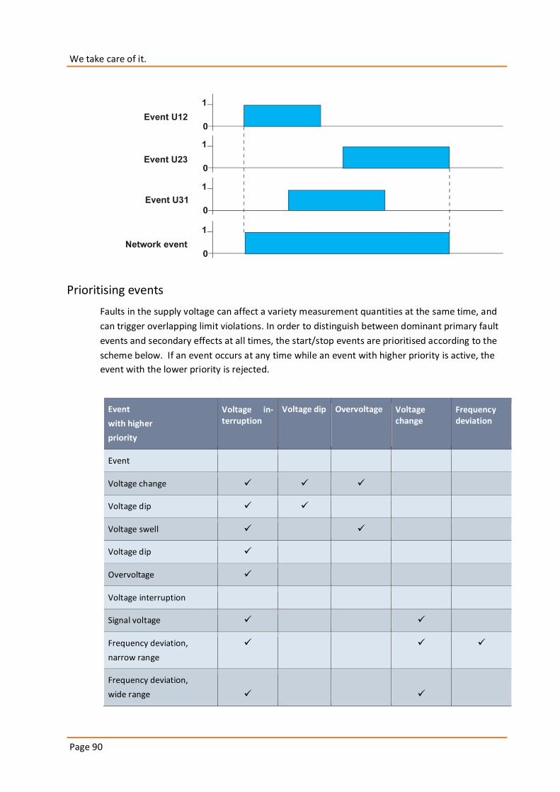
We take care of it.
Page 90
Prioritising events
Faults in the supply voltage can affect a variety measurement quantities at the same time, and
can trigger overlapping limit violations. In order to distinguish between dominant primary fault
events and secondary effects at all times, the start/stop events are prioritised according to the
scheme below. If an event occurs at any time while an event with higher priority is active, the
event with the lower priority is rejected.
Event
with higher
priority
Voltage in-terruption
Voltage dip Overvoltage Voltage change
Frequency deviation
Event
Voltage change
Voltage dip
Voltage swell
Voltage dip
Overvoltage
Voltage interruption
Signal voltage
Frequency deviation,
narrow range
Frequency deviation,
wide range
Page 91
Flagging
The PQI-DA network analyser flags measurement intervals in accordance with IEC 61000-4-30, Class
A.
Flags are generated for events that are based on the 10-ms r.m.s. values of the voltage.
The events are classified according to 3 fault levels:
Level Event
0 None
1 Fast voltage change, dip, swell
2 Voltage dip, overvoltage
3 Voltage interruption
For each phase voltage, the maximum fault level that occurs in each of the measurement intervals
(10/12 periods, 150/180 periods, 10-minute, 2-hour) is recorded and stored in a status word in the
interval data. By combining the maximum interval fault level with an adjustable threshold, it is de-
termined whether the events of the following features based on the interval measurement values
are evaluated or rejected:
Signal voltages (150/180-period values)
Network frequency (10-second value)
Slow voltage deviation (10-minute values)
Harmonics, THD (10-minute values)
Asymmetry (10-minute value)
Flicker (2-hour values)
The setting "Flagging from…" (WinPQ) sets the fault level
from which the events listed above are rejected. 10-minute and 2-hour events can only be re-
jected with the setting "Flagging from interruption" is selected (factory setting).
Binary event notification signals
The network events generate binary notification signals, which can be output via binary outputs, for
example.
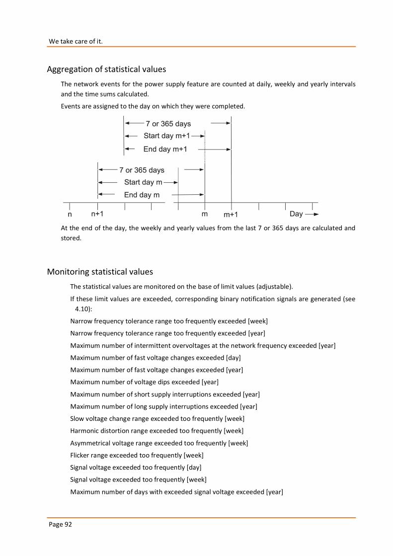
We take care of it.
Page 92
Aggregation of statistical values
The network events for the power supply feature are counted at daily, weekly and yearly intervals
and the time sums calculated.
Events are assigned to the day on which they were completed.
At the end of the day, the weekly and yearly values from the last 7 or 365 days are calculated and
stored.
Monitoring statistical values
The statistical values are monitored on the base of limit values (adjustable).
If these limit values are exceeded, corresponding binary notification signals are generated (see
4.10):
Narrow frequency tolerance range too frequently exceeded [week]
Narrow frequency tolerance range too frequently exceeded [year]
Maximum number of intermittent overvoltages at the network frequency exceeded [year]
Maximum number of fast voltage changes exceeded [day]
Maximum number of fast voltage changes exceeded [year]
Maximum number of voltage dips exceeded [year]
Maximum number of short supply interruptions exceeded [year]
Maximum number of long supply interruptions exceeded [year]
Slow voltage change range exceeded too frequently [week]
Harmonic distortion range exceeded too frequently [week]
Asymmetrical voltage range exceeded too frequently [week]
Flicker range exceeded too frequently [week]
Signal voltage exceeded too frequently [day]
Signal voltage exceeded too frequently [week]
Maximum number of days with exceeded signal voltage exceeded [year]
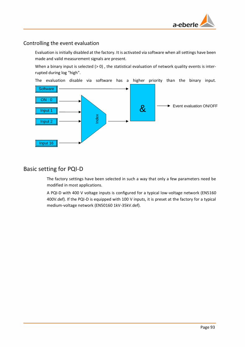
Page 93
Controlling the event evaluation
Evaluation is initially disabled at the factory. It is activated via software when all settings have been
made and valid measurement signals are present.
When a binary input is selected (> 0) , the statistical evaluation of network quality events is inter-
rupted during log "high".
The evaluation disable via software has a higher priority than the binary input.
Basic setting for PQI-D
The factory settings have been selected in such a way that only a few parameters need be
modified in most applications.
A PQI-D with 400 V voltage inputs is configured for a typical low-voltage network (EN5160
400V.def). If the PQI-D is equipped with 100 V inputs, it is preset at the factory for a typical
medium-voltage network (EN50160 1kV-35kV.def).
Input 1
Input 2
ON : 0
Input 16
Software
Ind
ex
& Event evaluation ON/OFF
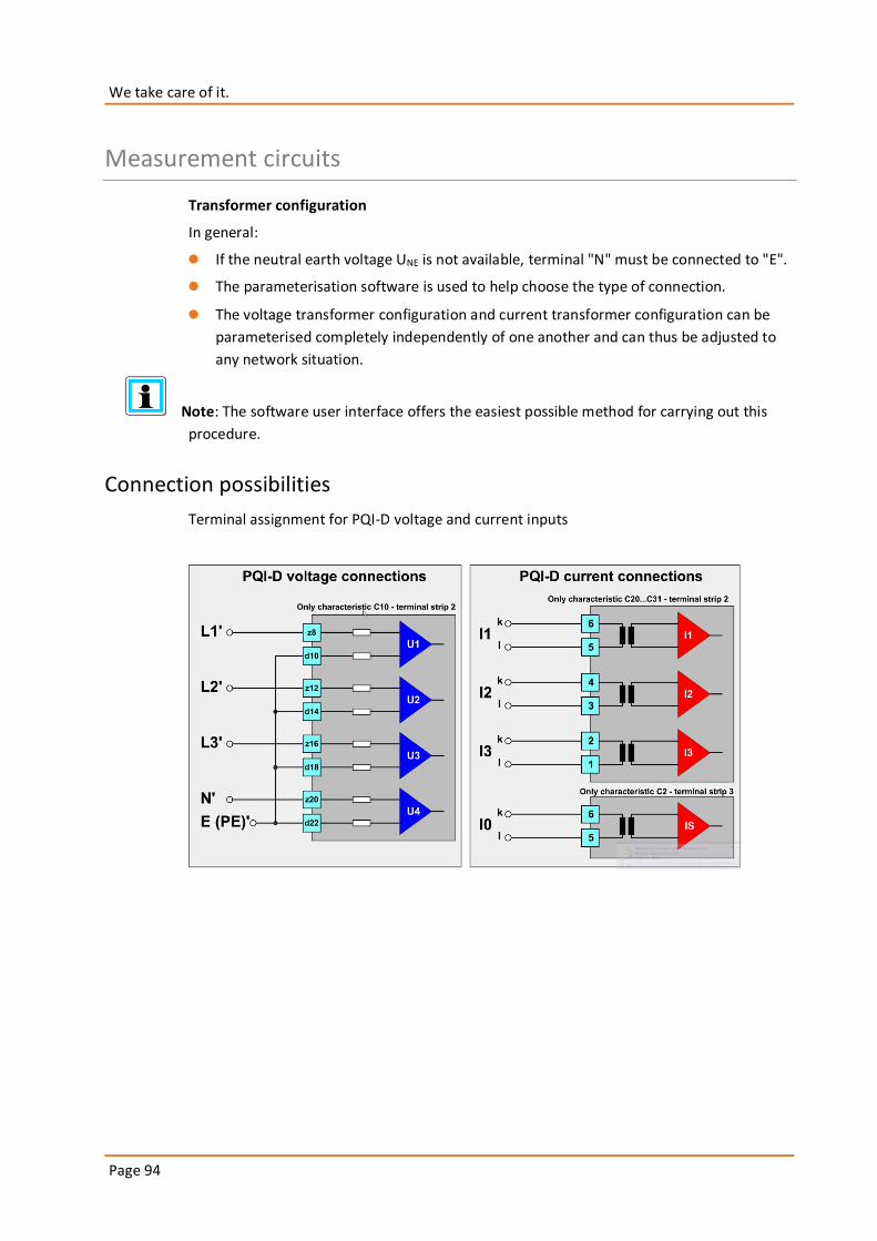
We take care of it.
Page 94
Measurement circuits
Transformer configuration
In general:
0 If the neutral earth voltage UNE is not available, terminal "N" must be connected to "E".
0 The parameterisation software is used to help choose the type of connection.
0 The voltage transformer configuration and current transformer configuration can be
parameterised completely independently of one another and can thus be adjusted to
any network situation.
Note: The software user interface offers the easiest possible method for carrying out this
procedure.
Connection possibilities
Terminal assignment for PQI-D voltage and current inputs
Page 95
Current transformer connections
Each PQI-D power quality interface has four current inputs. In general, inputs I1 to I3 can be
used to measure the conductor currents.
The fourth current can be used as a sum current or as a neutral conductor current input.
For sum current measurements, it does not matter whether the sum current is created using
a sum current transformer (core balance transformer) or a Holm-Green circuit.
Only two currents are required in an Aron circuit because, in “healthy” three-conductor net-
works (in which the vector sum of all three currents is zero), the third current can be
calculated if the other two currents are already known.
Normally, an Aron circuit is applied in such a way that the currents in L1 and L3 are measured
and are then used to calculate L2.
The PQI-D is not limited in this case either, since the appropriate input configuration is pre-
pared regardless of which phases have a current transformer available.
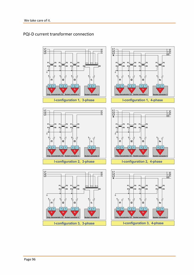
We take care of it.
Page 96
PQI-D current transformer connection
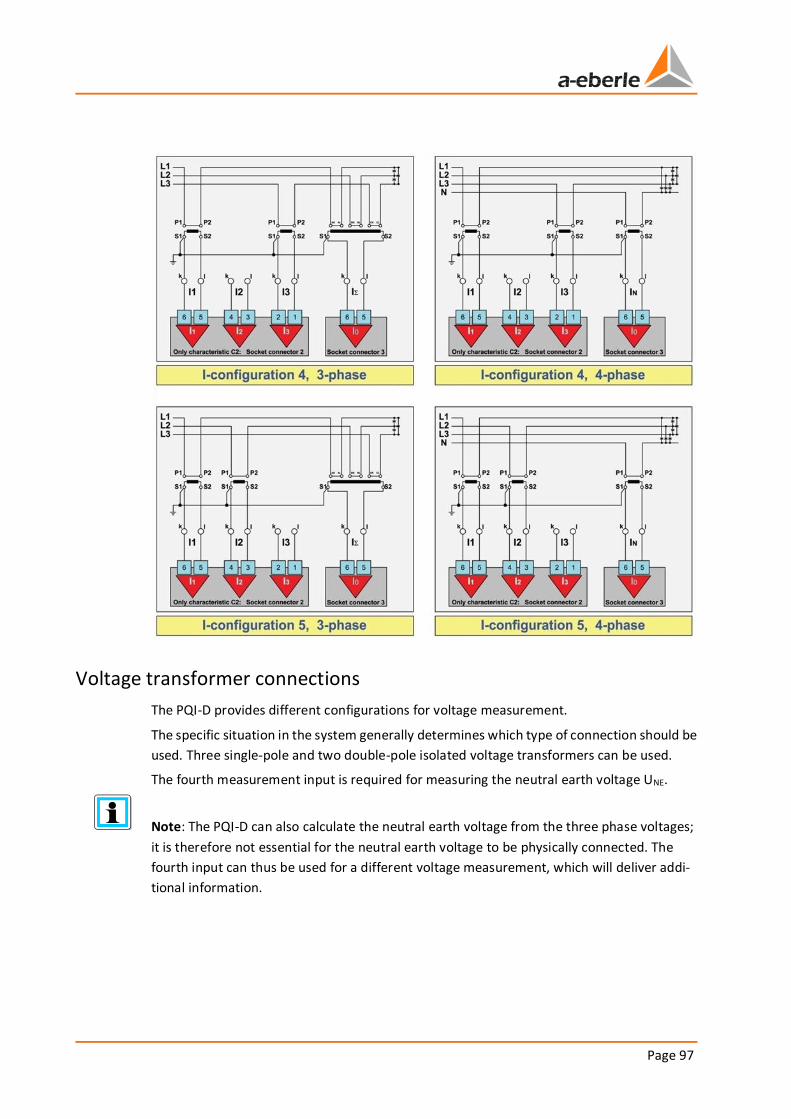
Page 97
Voltage transformer connections
The PQI-D provides different configurations for voltage measurement.
The specific situation in the system generally determines which type of connection should be
used. Three single-pole and two double-pole isolated voltage transformers can be used.
The fourth measurement input is required for measuring the neutral earth voltage UNE.
Note: The PQI-D can also calculate the neutral earth voltage from the three phase voltages;
it is therefore not essential for the neutral earth voltage to be physically connected. The
fourth input can thus be used for a different voltage measurement, which will deliver addi-
tional information.
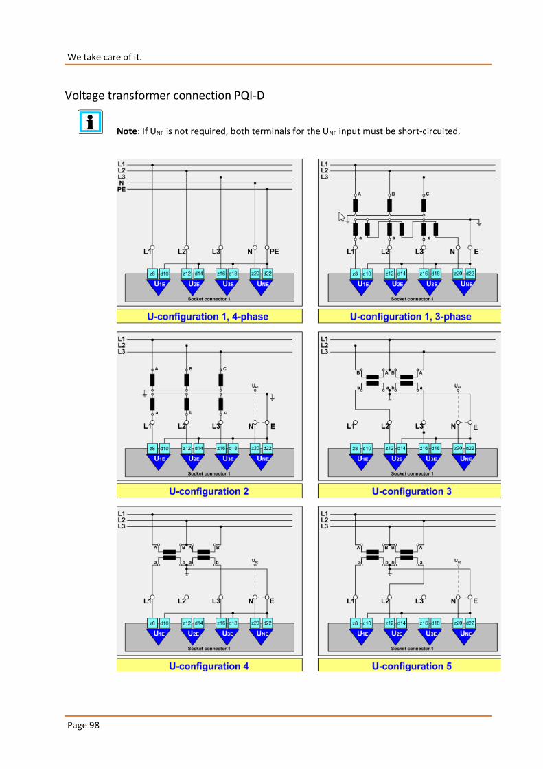
We take care of it.
Page 98
Voltage transformer connection PQI-D
Note: If UNE is not required, both terminals for the UNE input must be short-circuited.
Page 99
Reference voltage
U12 is set as the reference voltage at the factory. Any other voltage can also be defined as
the reference voltage. All absolute phase angles are based on this voltage.
The reference voltage is also used for frequency measurement.
In the 8xU version, the reference voltage is monitored and, if it fails, automatically
switched to the corresponding voltage of the other line, if one is available.
Network frequency
The nominal network frequency can be set to 50 Hz or 60 Hz.
The factory setting is 50 Hz.
Changes do not become effective until the device is restarted.
System time
The system time is set at the factory and is protected against unintentional adjustment; the
time zone is CET and summer/winter switching for CEST is activated.
If the local time zone does not match the one set at the factory, the setting can be changed
at any time.
Adapting the time to the local time zone must never be carried out manually!
The maximum time deviation in non-synchronised mode is 1 minute/month. When the time
setting is protected, the device accepts only changes within +/-250ppm based on the time
elapsed since the last correction. The time accuracy of 20ms required by DIN IEC 61000-4-
30, Class A dictates the need for synchronisation by an external real-time clock with DCF77
output (SPACE format) (refer to 6.4). In synchronised mode, the manual time setting is
blocked.
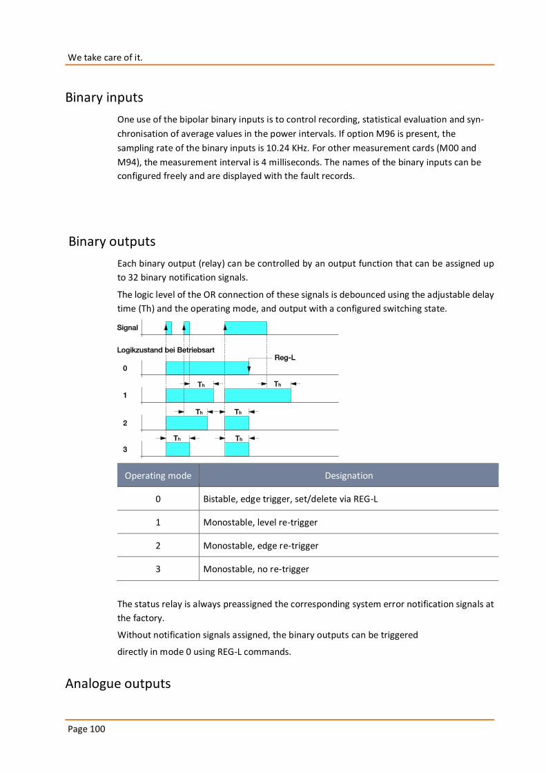
We take care of it.
Page 100
Binary inputs
One use of the bipolar binary inputs is to control recording, statistical evaluation and syn-
chronisation of average values in the power intervals. If option M96 is present, the
sampling rate of the binary inputs is 10.24 KHz. For other measurement cards (M00 and
M94), the measurement interval is 4 milliseconds. The names of the binary inputs can be
configured freely and are displayed with the fault records.
Binary outputs
Each binary output (relay) can be controlled by an output function that can be assigned up
to 32 binary notification signals.
The logic level of the OR connection of these signals is debounced using the adjustable delay
time (Th) and the operating mode, and output with a configured switching state.
Operating mode Designation
0 Bistable, edge trigger, set/delete via REG-L
1 Monostable, level re-trigger
2 Monostable, edge re-trigger
3 Monostable, no re-trigger
The status relay is always preassigned the corresponding system error notification signals at
the factory.
Without notification signals assigned, the binary outputs can be triggered
directly in mode 0 using REG-L commands.
Analogue outputs
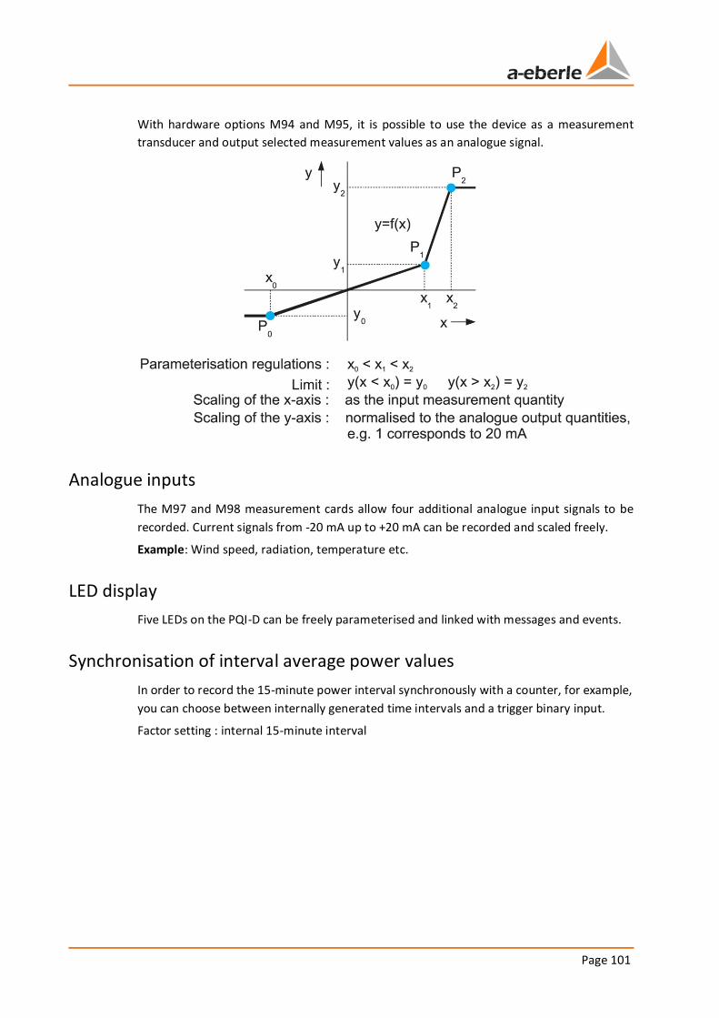
Page 101
With hardware options M94 and M95, it is possible to use the device as a measurement
transducer and output selected measurement values as an analogue signal.
Analogue inputs
The M97 and M98 measurement cards allow four additional analogue input signals to be
recorded. Current signals from -20 mA up to +20 mA can be recorded and scaled freely.
Example: Wind speed, radiation, temperature etc.
LED display
Five LEDs on the PQI-D can be freely parameterised and linked with messages and events.
Synchronisation of interval average power values
In order to record the 15-minute power interval synchronously with a counter, for example,
you can choose between internally generated time intervals and a trigger binary input.
Factor setting : internal 15-minute interval
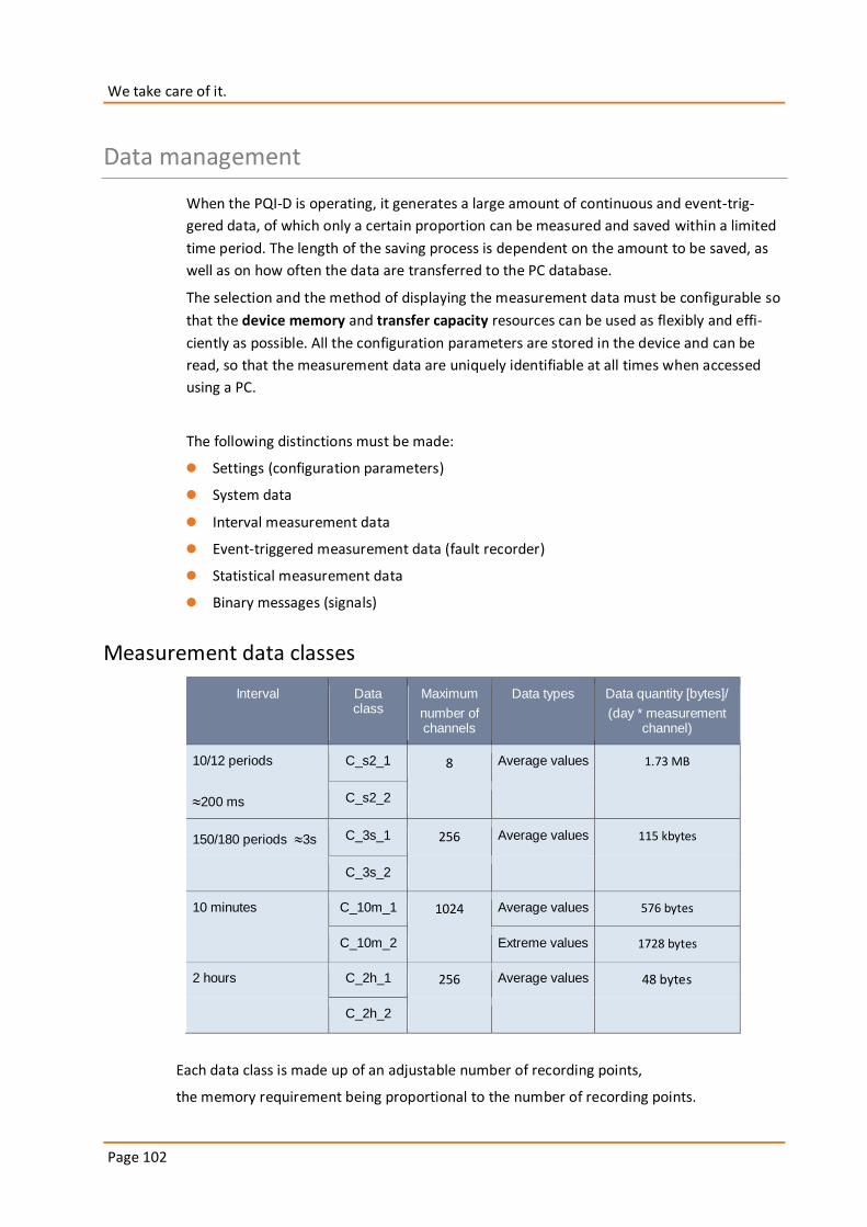
We take care of it.
Page 102
Data management
When the PQI-D is operating, it generates a large amount of continuous and event-trig-
gered data, of which only a certain proportion can be measured and saved within a limited
time period. The length of the saving process is dependent on the amount to be saved, as
well as on how often the data are transferred to the PC database.
The selection and the method of displaying the measurement data must be configurable so
that the device memory and transfer capacity resources can be used as flexibly and effi-
ciently as possible. All the configuration parameters are stored in the device and can be
read, so that the measurement data are uniquely identifiable at all times when accessed
using a PC.
The following distinctions must be made:
0 Settings (configuration parameters)
0 System data
0 Interval measurement data
0 Event-triggered measurement data (fault recorder)
0 Statistical measurement data
0 Binary messages (signals)
Measurement data classes
Interval Data class
Maximum
number of channels
Data types Data quantity [bytes]/
(day * measurement channel)
10/12 periods C_s2_1 8 Average values 1.73 MB
200 ms C_s2_2
150/180 periods 3s C_3s_1 256 Average values 115 kbytes
C_3s_2
10 minutes C_10m_1 1024 Average values 576 bytes
C_10m_2 Extreme values 1728 bytes
2 hours C_2h_1 256 Average values 48 bytes
C_2h_2
Each data class is made up of an adjustable number of recording points,
the memory requirement being proportional to the number of recording points.
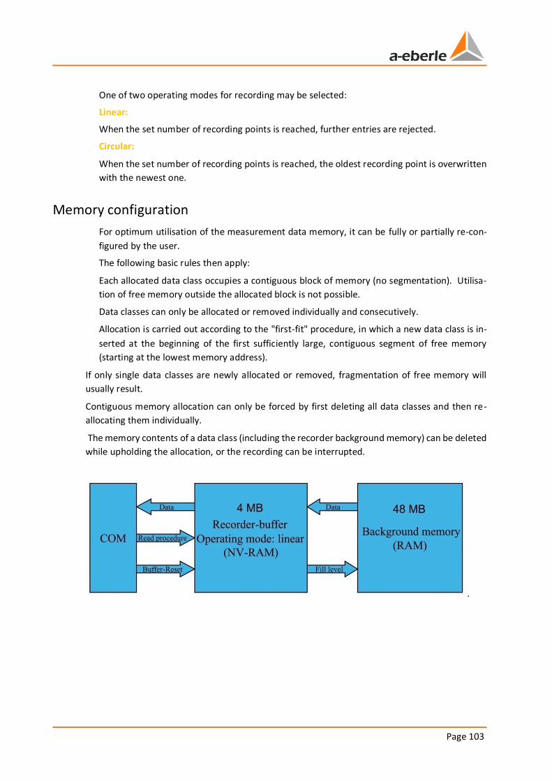
Page 103
One of two operating modes for recording may be selected:
Linear:
When the set number of recording points is reached, further entries are rejected.
Circular:
When the set number of recording points is reached, the oldest recording point is overwritten
with the newest one.
Memory configuration
For optimum utilisation of the measurement data memory, it can be fully or partially re-con-
figured by the user.
The following basic rules then apply:
Each allocated data class occupies a contiguous block of memory (no segmentation). Utilisa-
tion of free memory outside the allocated block is not possible.
Data classes can only be allocated or removed individually and consecutively.
Allocation is carried out according to the "first-fit" procedure, in which a new data class is in-
serted at the beginning of the first sufficiently large, contiguous segment of free memory
(starting at the lowest memory address).
If only single data classes are newly allocated or removed, fragmentation of free memory will
usually result.
Contiguous memory allocation can only be forced by first deleting all data classes and then re-
allocating them individually.
The memory contents of a data class (including the recorder background memory) can be deleted
while upholding the allocation, or the recording can be interrupted.
.
We take care of it.
Page 104
Besides the non-volatile NV RAM, a volatile background memory is also available in the consider-
ably larger SDRAM for the recording of fault records. All fault records are initially recorded in the
background memory. In order for them to be accessed from the device via the communication
interface, they must be shifted to the NV RAM.
In circular buffer mode, new fault records are shifted to the NV RAM buffer immediately, since
the oldest entry is always overwritten by the newest one, irrespective of whether it could be read
via the communication interface beforehand.
For this reason, the buffer for recorders A, B and S is set to linear mode at the
factory. Fault records are shifted from the background memory to the NV RAM buffer until the
latter is full. Further fault records are initially stored in the background memory. As soon as the
NV RAM buffer has been accessed, the corresponding memory is released and the next fault rec-
ords are shifted from background memory to NV RAM buffer. This ensures that no fault record
can be overwritten before it has been accessed.
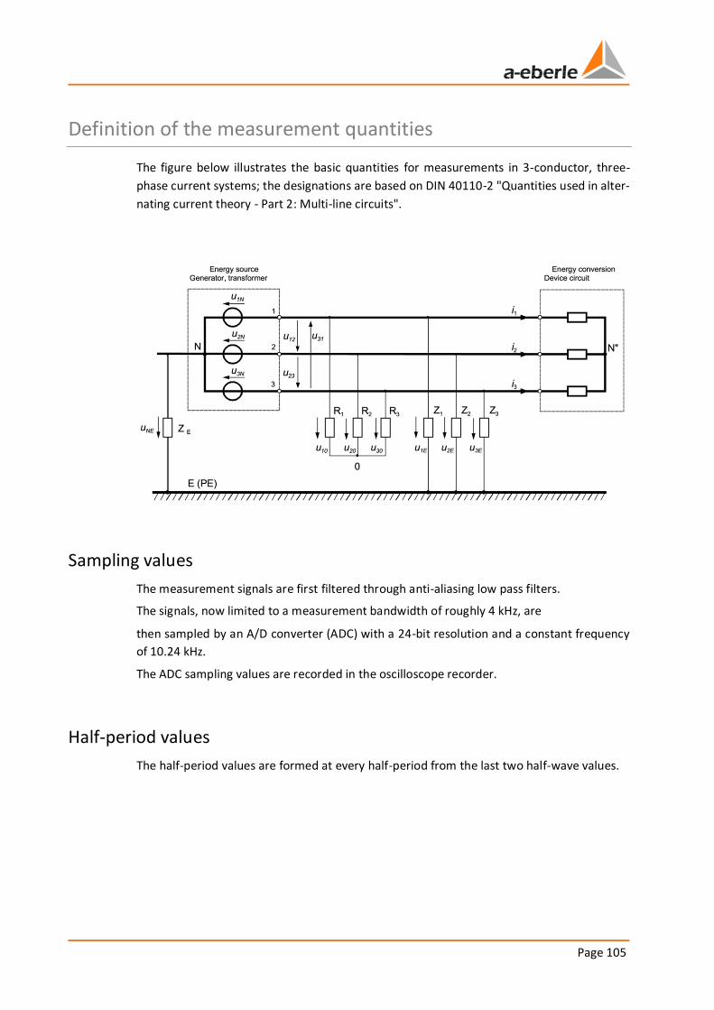
Page 105
Definition of the measurement quantities
The figure below illustrates the basic quantities for measurements in 3-conductor, three-
phase current systems; the designations are based on DIN 40110-2 "Quantities used in alter-
nating current theory - Part 2: Multi-line circuits".
Sampling values
The measurement signals are first filtered through anti-aliasing low pass filters.
The signals, now limited to a measurement bandwidth of roughly 4 kHz, are
then sampled by an A/D converter (ADC) with a 24-bit resolution and a constant frequency
of 10.24 kHz.
The ADC sampling values are recorded in the oscilloscope recorder.
Half-period values
The half-period values are formed at every half-period from the last two half-wave values.
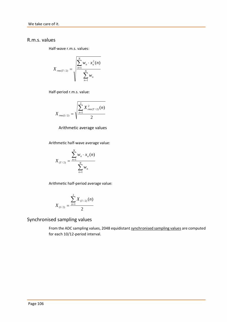
We take care of it.
Page 106
R.m.s. values
Half-wave r.m.s. values:
Half-period r.m.s. value:
Arithmetic average values
Arithmetic half-wave average value:
Arithmetic half-period average value:
Synchronised sampling values
From the ADC sampling values, 2048 equidistant synchronised sampling values are computed
for each 10/12-period interval.
N
n
n
N
n
an
Trms
w
nxw
X
1
1
2
)2/(
)(
2
)(2
1
2
)2/(
)2/1(
n
Trms
rms
nX
X
2
)(2
1
)2/(
)2/1(
n
T nX
X
N
n
n
N
n
an
T
w
nxw
X
1
1
)2/(
)(
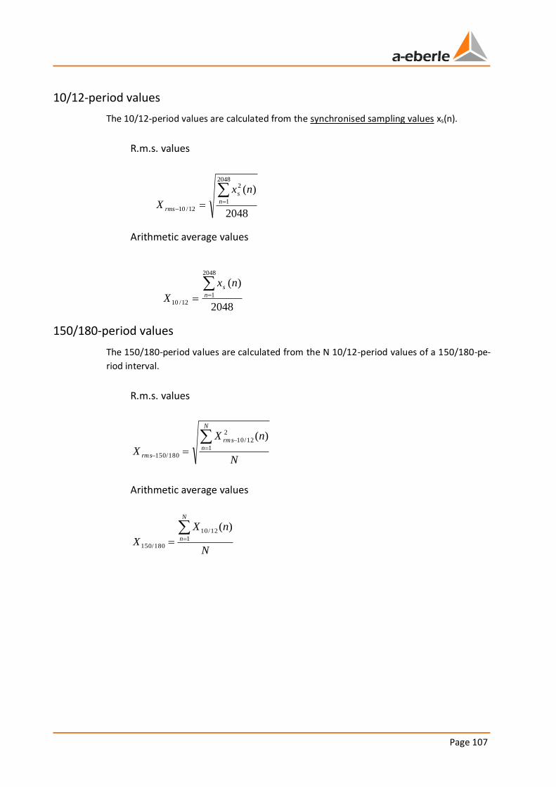
Page 107
10/12-period values
The 10/12-period values are calculated from the synchronised sampling values xs(n).
R.m.s. values
Arithmetic average values
150/180-period values
The 150/180-period values are calculated from the N 10/12-period values of a 150/180-pe-
riod interval.
R.m.s. values
N
nX
X
N
n
rms
rms
1
2
12/10
180/150
)(
Arithmetic average values
N
nX
X
N
n
1
12/10
180/150
)(
2048
)(2048
1
2
12/10
n
s
rms
nx
X
2048
)(2048
1
12/10
n
s nx
X
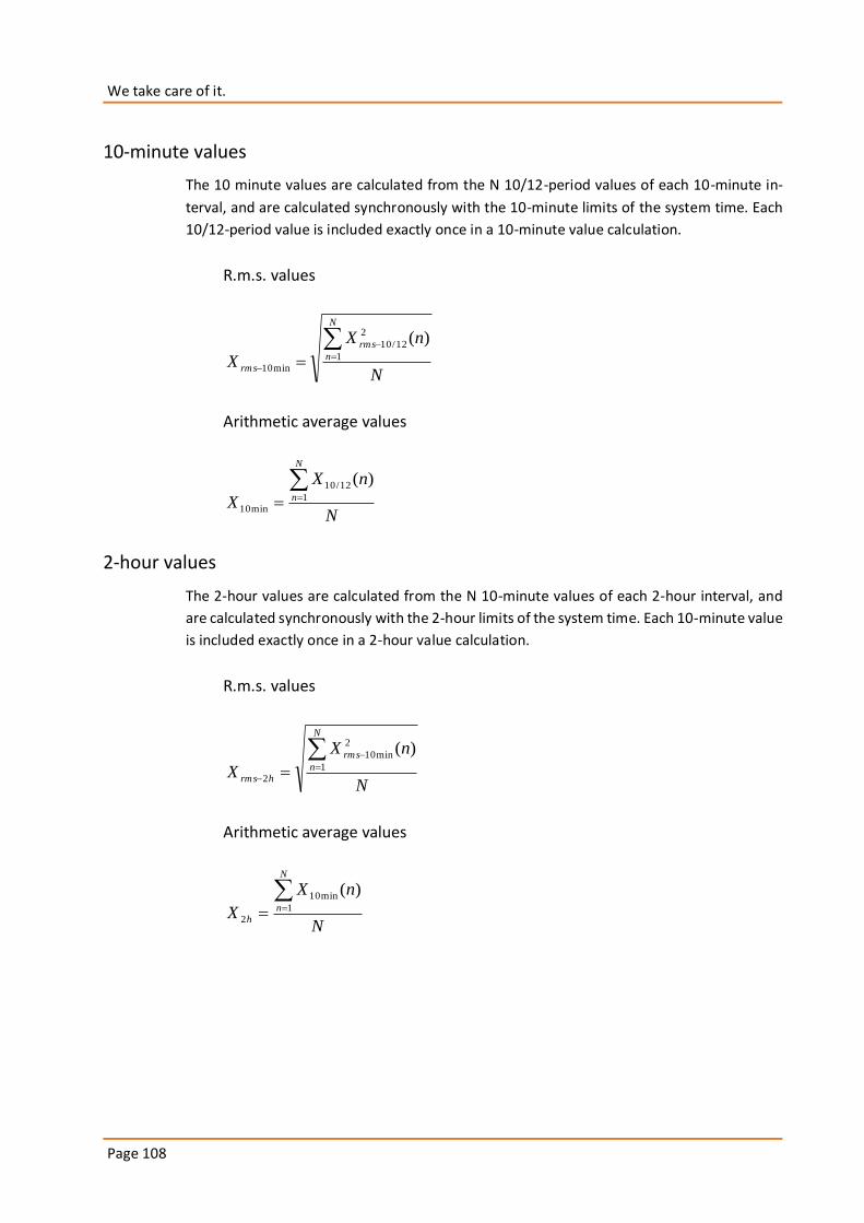
We take care of it.
Page 108
10-minute values
The 10 minute values are calculated from the N 10/12-period values of each 10-minute in-
terval, and are calculated synchronously with the 10-minute limits of the system time. Each
10/12-period value is included exactly once in a 10-minute value calculation.
R.m.s. values
N
nX
X
N
n
rms
rms
1
2
12/10
min10
)(
Arithmetic average values
N
nX
X
N
n
1
12/10
min10
)(
2-hour values
The 2-hour values are calculated from the N 10-minute values of each 2-hour interval, and
are calculated synchronously with the 2-hour limits of the system time. Each 10-minute value
is included exactly once in a 2-hour value calculation.
R.m.s. values
N
nX
X
N
n
rms
hrms
1
2
min10
2
)(
Arithmetic average values
N
nX
X
N
n
h
1
min10
2
)(
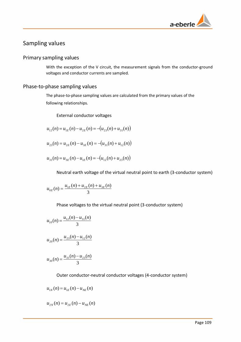
Page 109
Sampling values
Primary sampling values
With the exception of the V circuit, the measurement signals from the conductor-ground
voltages and conductor currents are sampled.
Phase-to-phase sampling values
The phase-to-phase sampling values are calculated from the primary values of the
following relationships.
External conductor voltages
)()()()()( 31232112 nununununu EE
)()()()()( 12313223 nununununu EE
)()()()()( 23121331 nununununu EE
Neutral earth voltage of the virtual neutral point to earth (3-conductor system)
3
)()()()( 321
0
nunununu EEE
E
Phase voltages to the virtual neutral point (3-conductor system)
3
)()()( 3112
10
nununu
3
)()()( 1223
20
nununu
3
)()()( 2331
30
nununu
Outer conductor-neutral conductor voltages (4-conductor system)
)()()( 11 nununu NEEN
)()()( 22 nununu NEEN
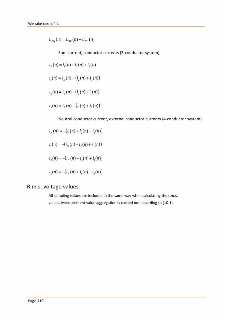
We take care of it.
Page 110
)()()( 33 nununu NEEN
Sum current, conductor currents (3-conductor system)
)()()()( 321 ninininiE
)()()()( 321 nininini E
)()()()( 132 nininini E
)()()()( 213 nininini E
Neutral conductor current, external conductor currents (4-conductor system)
)()()()( 321 ninininiN
)()()()( 321 nininini N
)()()()( 132 nininini N
)()()()( 213 nininini N
R.m.s. voltage values
All sampling values are included in the same way when calculating the r.m.s.
values. Measurement value aggregation is carried out according to (10.1).
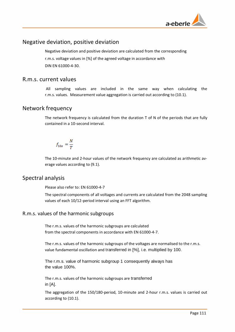
Page 111
Negative deviation, positive deviation
Negative deviation and positive deviation are calculated from the corresponding
r.m.s. voltage values in [%] of the agreed voltage in accordance with
DIN EN 61000-4-30.
R.m.s. current values
All sampling values are included in the same way when calculating the
r.m.s. values. Measurement value aggregation is carried out according to (10.1).
Network frequency
The network frequency is calculated from the duration T of N of the periods that are fully
contained in a 10-second interval.
The 10-minute and 2-hour values of the network frequency are calculated as arithmetic av-
erage values according to (9.1).
Spectral analysis
Please also refer to: EN 61000-4-7
The spectral components of all voltages and currents are calculated from the 2048 sampling
values of each 10/12-period interval using an FFT algorithm.
R.m.s. values of the harmonic subgroups
The r.m.s. values of the harmonic subgroups are calculated
from the spectral components in accordance with EN 61000-4-7.
The r.m.s. values of the harmonic subgroups of the voltages are normalised to the r.m.s.
value fundamental oscillation and transferred in [%], i.e. multiplied by 100.
The r.m.s. value of harmonic subgroup 1 consequently always has the value 100%.
The r.m.s. values of the harmonic subgroups are transferred
in [A].
The aggregation of the 150/180-period, 10-minute and 2-hour r.m.s. values is carried out
according to (10.1).
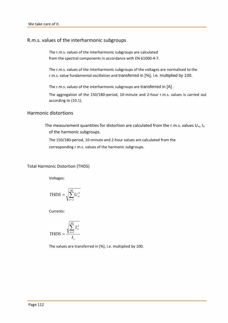
We take care of it.
Page 112
R.m.s. values of the interharmonic subgroups
The r.m.s. values of the interharmonic subgroups are calculated
from the spectral components in accordance with EN 61000-4-7.
The r.m.s. values of the interharmonic subgroups of the voltages are normalised to the
r.m.s. value fundamental oscillation and transferred in [%], i.e. multiplied by 100.
The r.m.s. values of the interharmonic subgroups are transferred in [A] .
The aggregation of the 150/180-period, 10-minute and 2-hour r.m.s. values is carried out
according to (10.1).
Harmonic distortions
The measurement quantities for distortion are calculated from the r.m.s. values Un, In
of the harmonic subgroups.
The 150/180-period, 10-minute and 2-hour values are calculated from the
corresponding r.m.s. values of the harmonic subgroups.
Total Harmonic Distortion (THDS)
Voltages:
40
2
2
n
nUTHDS
Currents:
1
40
2
2
I
I
THDSn
n
The values are transferred in [%], i.e. multiplied by 100.
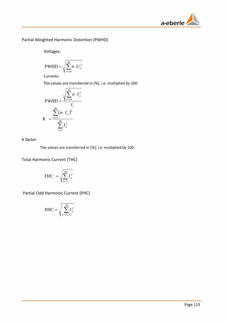
Page 113
Partial Weighted Harmonic Distortion (PWHD)
Voltages:
Currents:
The values are transferred in [%], i.e. multiplied by 100.
K factor
The values are transferred in [%], i.e. multiplied by 100.
Total Harmonic Current (THC)
40
2
2
n
nITHC
Partial Odd Harmonic Current (PHC)
39
23,21
2
n
nIPHC
40
14
2
n
nUnPWHD
1
40
14
2
I
In
PWHDn
n
40
1
2
40
1
2
n
n
n
n
I
In
K
We take care of it.
Page 114
Signal voltage
The 10/12-period r.m.s. value of the signal voltage based on the reference
voltage is calculated from the spectral components of the 10/12-period FFT using either one
of the two methods in DIN EN 61000-4-30.
The signal frequency can be selected within the measurement bandwidth.
The output is in [%].
The 10/12-period r.m.s. value is stored event-triggered in recorder S in accordance with DIN
EN 61000-4-30.
The 150/180-period r.m.s. value is formed according to (10.1) and is
a feature of the supply voltage (DIN 50160).
Phase of the voltages, currents to reference voltage (fundamental oscillation)
The 10/12-period value of the phase of the fundamental oscillations of the voltages and cur-
rents based on the reference voltage is calculated from the phase angles of the
corresponding spectral components.
The phase angle of the reference voltage is consequently always 0°.
The 150/180-period, 10-minute and 2-hour values are calculated as arithmetic average val-
ues according to (10.1).
Phase of the phase voltages to associated conductor currents (fundamental oscil-
lation)
The 10/12-period value of the phase of the fundamental oscillations of the phase voltages
based on the associated conductor currents is calculated from the phase angles of the corre-
sponding spectral components.
The 150/180-period, 10-minute and 2-hour values are calculated as arithmetic average val-
ues according to (10.1).
Phase of the current harmonics to the phase voltage fundamental oscillation
For the 2nd..40th harmonics of the conductor currents, the phase shift (+/- 180°) of the
zero point is calculated based on the zero point of the fundamental oscillation of the associ-
ated phase voltage (10/12-period value).
The 150/180-period, 10-minute and 2-hour values are calculated as arithmetic average val-
ues according to (10.1).
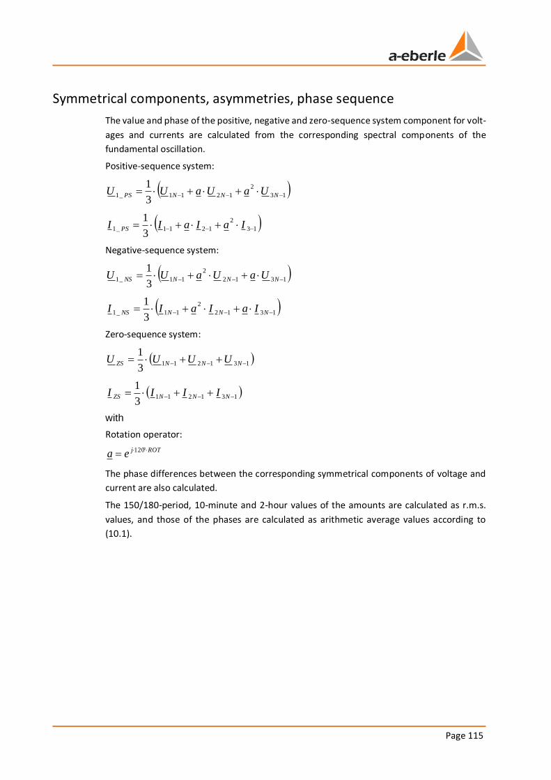
Page 115
Symmetrical components, asymmetries, phase sequence
The value and phase of the positive, negative and zero-sequence system component for volt-
ages and currents are calculated from the corresponding spectral components of the
fundamental oscillation.
Positive-sequence system:
13
2
1211_13
1 NNNPS UaUaUU
13
2
1211_13
1 IaIaII PS
Negative-sequence system:
1312
2
11_13
1 NNNNS UaUaUU
1312
2
11_13
1 NNNNS IaIaII
Zero-sequence system:
1312113
1 NNNZS UUUU
1312113
1 NNNZS IIII
with
Rotation operator:
ROTjea 120
The phase differences between the corresponding symmetrical components of voltage and
current are also calculated.
The 150/180-period, 10-minute and 2-hour values of the amounts are calculated as r.m.s.
values, and those of the phases are calculated as arithmetic average values according to
(10.1).
We take care of it.
Page 116
The negative-sequence system asymmetry is calculated from the negative-sequence and pos-
itive-sequence system components.
Voltage:
Current:
The zero-sequence system asymmetry is calculated from the zero-sequence and
positive-sequence system components.
Voltage
Current
All asymmetry values are transferred in [%], i.e. multiplied by 100.
The 150/180-period, 10-minute and 2-hour values are calculated as arithmetic average val-
ues according to (10.1).
When calculating the symmetrical components, the direction of rotation
ROT is selected in such a way that the positive-sequence component of the voltage is larger
than the negative-sequence system component.
ROT = +1 : phase sequence 123 ROT = -1 : phase sequence 321
PS
NS
U
Uu
_1
_1
2
PS
NS
I
Iu
_1
_1
2
PS
ZS
U
Uu
_1
0
PS
ZS
I
Iu
_1
0
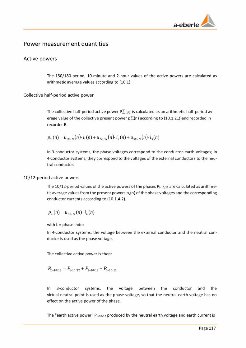
Page 117
Power measurement quantities
Active powers
The 150/180-period, 10-minute and 2-hour values of the active powers are calculated as
arithmetic average values according to (10.1).
Collective half-period active power
The collective half-period active power P(1/2) is calculated as an arithmetic half-period av-
erage value of the collective present power p(n) according to (10.1.2.2)and recorded in
recorder B.
In 3-conductor systems, the phase voltages correspond to the conductor-earth voltages; in
4-conductor systems, they correspond to the voltages of the external conductors to the neu-
tral conductor.
10/12-period active powers
The 10/12-period values of the active powers of the phases PL-10/12 are calculated as arithme-
tic average values from the present powers pL(n) of the phase voltages and the corresponding
conductor currents according to (10.1.4.2).
)()()( /0 ninunp LNLL
with L = phase index
In 4-conductor systems, the voltage between the external conductor and the neutral con-
ductor is used as the phase voltage.
The collective active power is then:
12/10312/10212/10112/10 PPPP
In 3-conductor systems, the voltage between the conductor and the
virtual neutral point is used as the phase voltage, so that the neutral earth voltage has no
effect on the active power of the phase.
The "earth active power" PE-10/12 produced by the neutral earth voltage and earth current is
)()()()( 3/32/21/1 ninuninuninunp NENENE
We take care of it.
Page 118
calculated separately as an arithmetic average value from the present powers pE(n) of the
neutral earth voltage and the earth current according to (10.1.4.2).
)()()( 0 ninunp EEE
The collective active power is then calculated as
12/1012/10312/10212/10112/10 EPPPPP
The fundamental oscillation active power is calculated from the apparent power of the geo-
metrical fundamental oscillation (refer to 10.9.2) as
12/1012/10 Re GG SP
Interval average values of the active powers
The average values of the active powers of the phases and the collective active power are
based on a definable time interval and transferred as events. The time interval can be trig-
gered either externally (binary input/trigger command) or internally as a fixed cycle time.
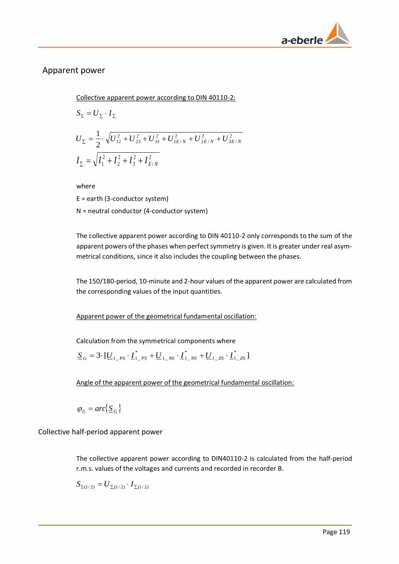
Page 119
Apparent power
Collective apparent power according to DIN 40110-2:
where
E = earth (3-conductor system)
N = neutral conductor (4-conductor system)
The collective apparent power according to DIN 40110-2 only corresponds to the sum of the
apparent powers of the phases when perfect symmetry is given. It is greater under real asym-
metrical conditions, since it also includes the coupling between the phases.
The 150/180-period, 10-minute and 2-hour values of the apparent power are calculated from
the corresponding values of the input quantities.
Apparent power of the geometrical fundamental oscillation:
Calculation from the symmetrical components where
][3*
_1_1
*
_1_1
*
_1_1 ZSZSNSNSPSPSG IUIUIUS
Angle of the apparent power of the geometrical fundamental oscillation:
GG Sarc
Collective half-period apparent power
The collective apparent power according to DIN40110-2 is calculated from the half-period
r.m.s. values of the voltages and currents and recorded in recorder B.
2
/
2
3
2
2
2
1 NEIIIII
2
/3
2
/2
2
/1
2
31
2
23
2
122
1NENENE UUUUUUU
IUS
)2/1()2/1()2/1( IUS
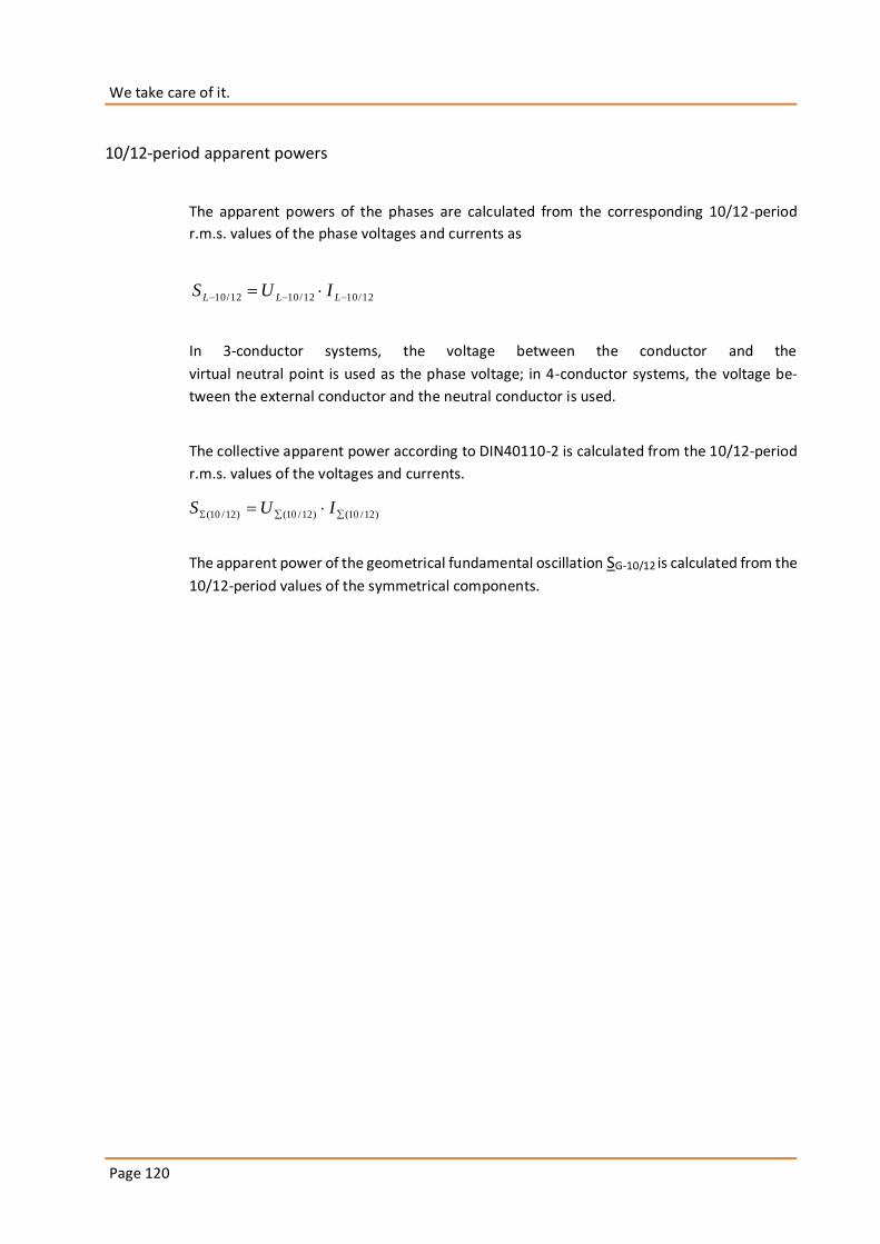
We take care of it.
Page 120
10/12-period apparent powers
The apparent powers of the phases are calculated from the corresponding 10/12-period
r.m.s. values of the phase voltages and currents as
12/1012/1012/10 LLL IUS
In 3-conductor systems, the voltage between the conductor and the
virtual neutral point is used as the phase voltage; in 4-conductor systems, the voltage be-
tween the external conductor and the neutral conductor is used.
The collective apparent power according to DIN40110-2 is calculated from the 10/12-period
r.m.s. values of the voltages and currents.
The apparent power of the geometrical fundamental oscillation SG-10/12 is calculated from the
10/12-period values of the symmetrical components.
)12/10()12/10()12/10( IUS
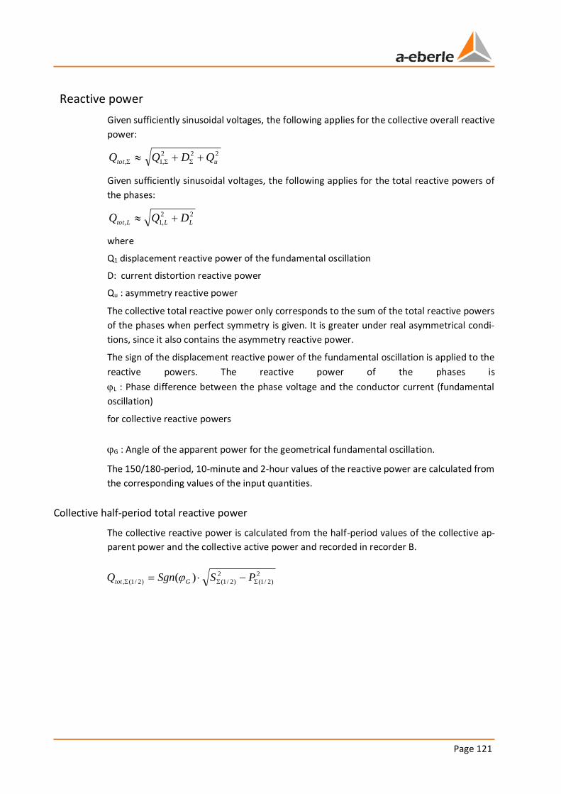
Page 121
Reactive power
Given sufficiently sinusoidal voltages, the following applies for the collective overall reactive
power:
222
,1, utot QDQQ
Given sufficiently sinusoidal voltages, the following applies for the total reactive powers of
the phases:
22
,1, LLLtot DQQ
where
Q1 displacement reactive power of the fundamental oscillation
D: current distortion reactive power
Qu : asymmetry reactive power
The collective total reactive power only corresponds to the sum of the total reactive powers
of the phases when perfect symmetry is given. It is greater under real asymmetrical condi-
tions, since it also contains the asymmetry reactive power.
The sign of the displacement reactive power of the fundamental oscillation is applied to the
reactive powers. The reactive power of the phases is
L : Phase difference between the phase voltage and the conductor current (fundamental
oscillation)
for collective reactive powers
G : Angle of the apparent power for the geometrical fundamental oscillation.
The 150/180-period, 10-minute and 2-hour values of the reactive power are calculated from
the corresponding values of the input quantities.
Collective half-period total reactive power
The collective reactive power is calculated from the half-period values of the collective ap-
parent power and the collective active power and recorded in recorder B.
2
)2/1(
2
)2/1()2/1(, )( PSSgnQ Gtot
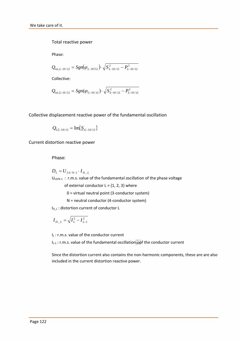
We take care of it.
Page 122
Total reactive power
Phase:
Collective:
Collective displacement reactive power of the fundamental oscillation
12/1012/10,1 Im GSQ
Current distortion reactive power
Phase:
UL0/N-1 : r.m.s. value of the fundamental oscillation of the phase voltage
of external conductor L = 1, 2, 3 where
0 = virtual neutral point (3-conductor system)
N = neutral conductor (4-conductor system)
ID_L : distortion current of conductor L
IL : r.m.s. value of the conductor current
IL-1 : r.m.s. value of the fundamental oscillation of the conductor current
Since the distortion current also contains the non-harmonic components, these are are also
included in the current distortion reactive power.
2
12/10
2
12/101071212/10, LLLLtot PSSgnQ
2
12/10
2
12/1012/1012/10, )( PSSgnQ Gtot
LDNLL IUD _1/0
2
1
2
_ LLLD III
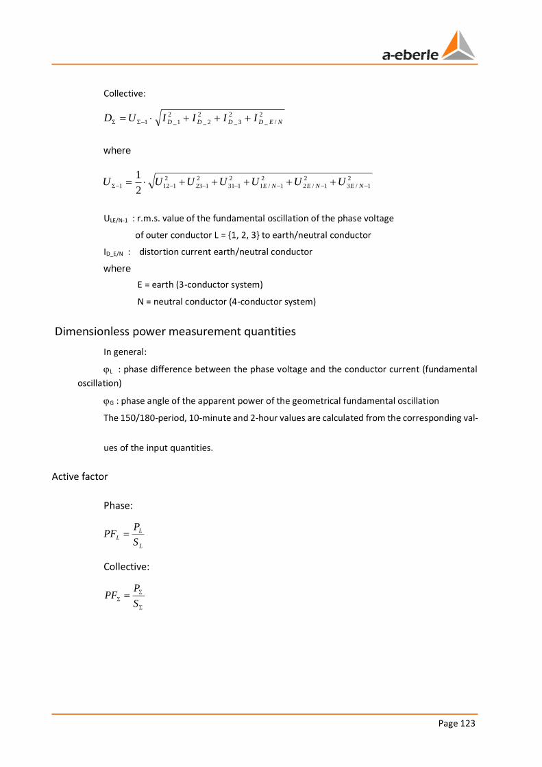
Page 123
Collective:
where
ULE/N-1 : r.m.s. value of the fundamental oscillation of the phase voltage
of outer conductor L = 1, 2, 3 to earth/neutral conductor
ID_E/N : distortion current earth/neutral conductor
where
E = earth (3-conductor system)
N = neutral conductor (4-conductor system)
Dimensionless power measurement quantities
In general:
L : phase difference between the phase voltage and the conductor current (fundamental
oscillation)
G : phase angle of the apparent power of the geometrical fundamental oscillation
The 150/180-period, 10-minute and 2-hour values are calculated from the corresponding val-
ues of the input quantities.
Active factor
Phase:
Collective:
2
/_
2
3_
2
2_
2
1_1 NEDDDD IIIIUD
2
1/3
2
1/2
2
1/1
2
131
2
123
2
11212
1 NENENE UUUUUUU
L
LL
S
PPF
S
PPF
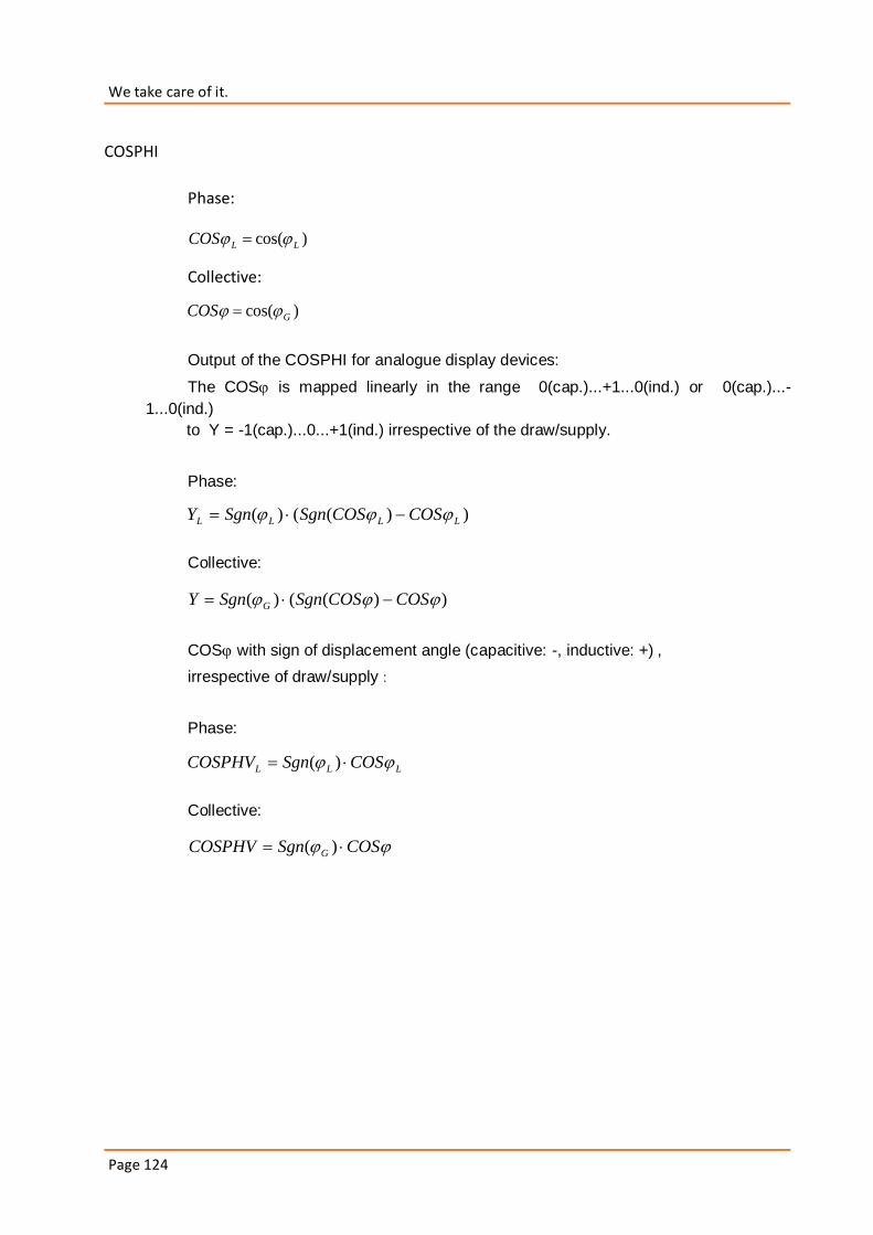
We take care of it.
Page 124
COSPHI
Phase:
Collective:
Output of the COSPHI for analogue display devices:
The COS is mapped linearly in the range 0(cap.)...+1...0(ind.) or 0(cap.)...-
1...0(ind.)
to Y = -1(cap.)...0...+1(ind.) irrespective of the draw/supply.
Phase:
Collective:
COS with sign of displacement angle (capacitive: -, inductive: +) ,
irrespective of draw/supply :
Phase:
Collective:
)cos( LLCOS
)cos( GCOS
))(()( LLLL COSCOSSgnSgnY
))(()( COSCOSSgnSgnY G
LLL COSSgnCOSPHV )(
COSSgnCOSPHV G )(
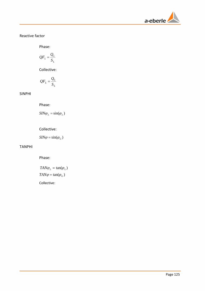
Page 125
Reactive factor
Phase:
Collective:
SINPHI
Phase:
Collective:
TANPHI
Phase:
Collective:
L
L
LS
QQF
S
QQF
)sin( LLSIN
)sin( GSIN
)tan( LLTAN
)tan( GTAN
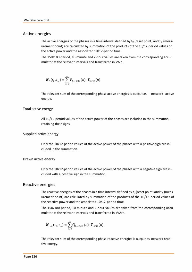
We take care of it.
Page 126
Active energies
The active energies of the phases in a time interval defined by t0 (reset point) and tm (meas-
urement point) are calculated by summation of the products of the 10/12-period values of
the active power and the associated 10/12-period time.
The 150/180-period, 10-minute and 2-hour values are taken from the corresponding accu-
mulator at the relevant intervals and transferred in kWh.
The relevant sum of the corresponding phase active energies is output as network active
energy.
Total active energy
All 10/12-period values of the active power of the phases are included in the summation,
retaining their signs.
Supplied active energy
Only the 10/12-period values of the active power of the phases with a positive sign are in-
cluded in the summation.
Drawn active energy
Only the 10/12-period values of the active power of the phases with a negative sign are in-
cluded with a positive sign in the summation.
Reactive energies
The reactive energies of the phases in a time interval defined by t0 (reset point) and tm (meas-
urement point) are calculated by summation of the products of the 10/12-period values of
the reactive power and the associated 10/12-period time.
The 150/180-period, 10-minute and 2-hour values are taken from the corresponding accu-
mulator at the relevant intervals and transferred in kVArh.
The relevant sum of the corresponding phase reactive energies is output as network reac-
tive energy.
m
n
LmL nTnPttW0
12/1012/100 )()(),(
m
n
LmLr nTnQttW0
12/1012/100 )()(),(
Page 127
Total reactive energy
All 10/12-period values of the reactive power of the phases are included in the summation,
retaining their signs.
Supplied reactive energy
Only the 10/12-period values of the reactive power of the phases with a positive sign are
included in the summation.
Drawn reactive energy
Only the 10/12-period values of the reactive power of the phases with a negative sign are
included with a positive sign in the summation.
Flicker magnitude
The short-term flicker magnitudes Pst (10 minutes) and long-term flicker magnitudes Plt (2
hours) are calculated for the phase and delta voltages. Pst and Plt are defined in EN 61000-4-
15.
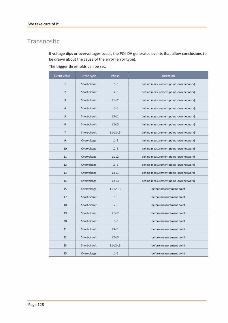
We take care of it.
Page 128
Transnostic
If voltage dips or overvoltages occur, the PQI-DA generates events that allow conclusions to
be drawn about the cause of the error (error type).
The trigger thresholds can be set.
Event value Error type Phase Direction
1 Short-circuit L1-E behind measurement point (own network)
2 Short-circuit L2-E behind measurement point (own network)
3 Short-circuit L1-L2 behind measurement point (own network)
4 Short-circuit L3-E behind measurement point (own network)
5 Short-circuit L3-L1 behind measurement point (own network)
6 Short-circuit L2-L3 behind measurement point (own network)
7 Short-circuit L1-L2-L3 behind measurement point (own network)
9 Overvoltage L1-E behind measurement point (own network)
10 Overvoltage L2-E behind measurement point (own network)
11 Overvoltage L1-L2 behind measurement point (own network)
12 Overvoltage L3-E behind measurement point (own network)
13 Overvoltage L3-L1 behind measurement point (own network)
14 Overvoltage L2-L3 behind measurement point (own network)
15 Overvoltage L1-L2-L3 before measurement point
17 Short-circuit L1-E before measurement point
18 Short-circuit L2-E before measurement point
19 Short-circuit L1-L2 before measurement point
20 Short-circuit L3-E before measurement point
21 Short-circuit L3-L1 before measurement point
22 Short-circuit L2-L3 before measurement point
23 Short-circuit L1-L2-L3 before measurement point
25 Overvoltage L1-E before measurement point
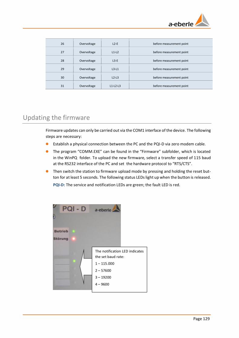
Page 129
26 Overvoltage L2-E before measurement point
27 Overvoltage L1-L2 before measurement point
28 Overvoltage L3-E before measurement point
29 Overvoltage L3-L1 before measurement point
30 Overvoltage L2-L3 before measurement point
31 Overvoltage L1-L2-L3 before measurement point
Updating the firmware
Firmware updates can only be carried out via the COM1 interface of the device. The following
steps are necessary:
0 Establish a physical connection between the PC and the PQI-D via zero modem cable.
0 The program “COMM.EXE” can be found in the “Firmware” subfolder, which is located
in the WinPQ folder. To upload the new firmware, select a transfer speed of 115 baud
at the RS232 interface of the PC and set the hardware protocol to “RTS/CTS”.
0 Then switch the station to firmware upload mode by pressing and holding the reset but-
ton for at least 5 seconds. The following status LEDs light up when the button is released.
PQI-D: The service and notification LEDs are green; the fault LED is red.
The notification LED indicates
the set baud rate:
1 – 115.000
2 – 57600
3 – 19200
4 – 9600
We take care of it.
Page 130
0 In the program “COMM.EXE” menu: Select “Send terminal/firmware with reset”.
0 The familiar Windows “Open file dialog” is shown. The valid firmware file (e.g.
PQI_UU.MOT) must be opened.
The "Operation" LED flashes once per second during data transfer.
The status of the upload can be followed in the program status line.
0 Then (transfer takes approx. 3 to 5 minutes), the device restarts. As soon as the "Oper-
ation" LED lights up again, it is possible to query the version at the terminal using the
“VER” command. The response must contain the new firmware version with the asso-
ciated date, e.g. "PQI-D: Version 5.0.09 from 13.01.11"
0 You can use the terminal command "SYSRESET=590" to load the current factory set-
tings. The station is then restarted. The station parameterisations are then restored via
one of the communication interfaces using the “PQPara”program components.
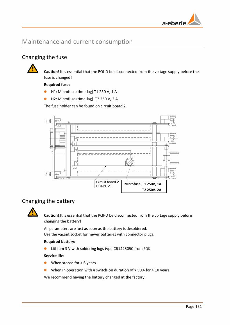
Page 131
Maintenance and current consumption
Changing the fuse
Caution! It is essential that the PQI-D be disconnected from the voltage supply before the
fuse is changed!
Required fuses:
0 H1: Microfuse (time-lag) T1 250 V, 1 A
0 H2: Microfuse (time-lag) T2 250 V, 2 A
The fuse holder can be found on circuit board 2.
Changing the battery
Caution! It is essential that the PQI-D be disconnected from the voltage supply before
changing the battery!
All parameters are lost as soon as the battery is desoldered.
Use the vacant socket for newer batteries with connector plugs.
Required battery:
0 Lithium 3 V with soldering lugs type CR1425050 from FDK
Service life:
0 When stored for > 6 years
0 When in operation with a switch-on duration of > 50% for > 10 years
We recommend having the battery changed at the factory.
Microfuse T1 250V, 1A
T2 250V, 2A
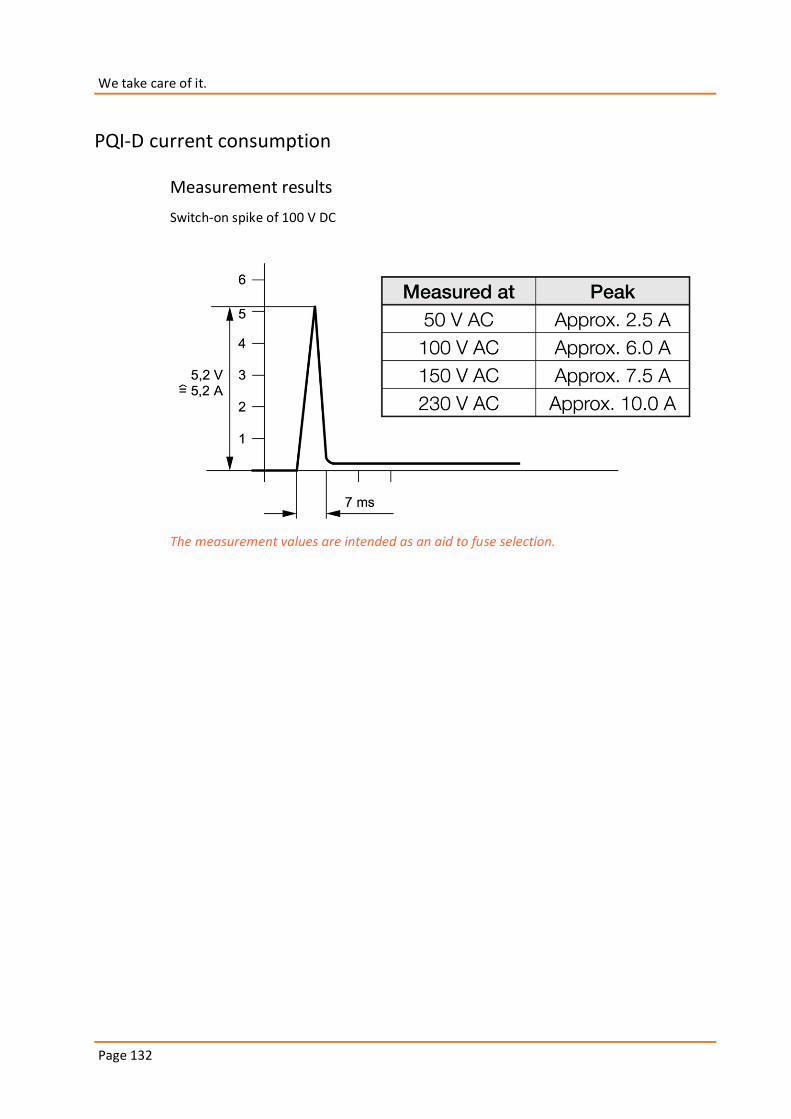
We take care of it.
Page 132
PQI-D current consumption
Measurement results
Switch-on spike of 100 V DC
The measurement values are intended as an aid to fuse selection.
Page 133
Scope of delivery
0 PQI-D corresponding to the design features
0 Operating manual
0 Supplement
0 CD (operating manual, PQ Para Express software)
Commissioning instructions
Storage information
The devices should be stored in clean, dry rooms. The devices and their respective replace-
ment modules can be stored between -25°C and +65°C.
The relative humidity must not lead to the formation of either condensation or ice.
We recommend that the storage temperature be kept between +0°C and +55°C to ensure
that the built-in electrolytic capacitors do not age prematurely.
We also recommend that the device be connected to an auxiliary voltage every two years to
reform the electrolytic capacitors. This procedure should also be carried out before the de-
vice is put into operation. Under extreme climatic conditions (tropics), this also ensures “pre-
heating” at the same time and helps to avoid the formation of condensation.
The device should be stored in the service room for at least two hours prior to being con-
nected to the voltage for the first time, so that it can become accustomed to the ambient
temperature and to avoid the formation of moisture and condensation.
Guarantee
The guarantee is valid for three years from the date of delivery.
We take care of it.
Page 134
Ordering information
Please note the following when ordering:
0 Only one code with the same capital letter is possible.
0 If the capital letter is followed by the number 9, additional details in plain text are re-
quired.
0 If capital letters are followed only by zeros, the code can be omitted.
FEATURE CODE
Power quality interface for medium and high voltage networks
0 according to DIN EN 50160 and IEC 61000-4-30 0 with two E-LAN interfaces for communication 0 with REGSys components REG-D(A), PAN-D, REG-DP(A), MMU-D, EOR-D and REG-DM. The standard version is equipped with COM 1, COM 2 and COM 3
PQI-D
Design
0 19" plug-in module (18TE/3HE) 0 Wall mounting housing (20TE)
0 Panel mounting housing (30TE) 0 19" frame or wall mounting housing (30TE, 49TE) Wiring according to agreement
B01 B90 B91 B92
Supply voltage
0 AC 100V ... 110V ... 240V / DC 100V..220V..300V
0 DC 20V...60V...70V
H1 H2
Input configuration
0 4 voltage transformers 0 2 x 4 voltage transformers
0 4 voltage transformers, 4 current transformers In = 1A (Imax < 2 x In) 0 4 voltage transformers, 4 current transformers In=1A (Imax < 20 x In) 0 4 voltage transformers, 4 current transformers In=5A (Imax < 2 x In) 0 4 voltage transformers, 4 current transformers In=5A (Imax < 20 x In)
0 4 voltage transformers, 4 current inputs for Rogowski coils 0 4 voltage transformers, 4 current inputs for mini current clamps
C00 C10
C20 C21 C30 C31 C40 C41
Rated value of the input voltage
0 100 V / 110 V 0 230 V / 400 V other rated voltages (e.g. 4 x 100 V and 4 x 400 V)
E1
E2 E9
Additional inputs and outputs
0 with 5 programmable relays plus life contact 16 programmable binary inputs (48…250 V AC/DC) (additional voltage ranges possible on request)
0 With 3 programmable relays plus life contacts 4 programmable mA outputs and 6 programmable binary inputs Note: Please specify the nominal voltage for the binary inputs!
0 with 7 programmable relays plus life contact
0 with 8 programmable mA outputs 0 with 6 analogue mA outputs and 2 binary outputs plus life contact
M00 M92
M93
M94 M95
Page 135
FEATURE CODE
0 with 5 relays plus life contact, 16 binary inputs for DC signals (48 V…250 V) with time stamp accuracy of +20 ms
(additional voltage ranges possible on request) 0 with one programmable relay contact (e.g. life contact)
16 programmable binary inputs (10 … 50 V AC/DC) 4 analogue inputs (0... 10 V / 4 ... 20 mA)
0 with one programmable relay contact (e.g. life contact) 16 programmable inputs (48 … 250 V AC/DC) 4 analogue inputs (0 ... 10 V / 4 ... 20 mA)
M96
M97
M98
Operating manual
0 German
0 English 0 French
G1
G2 G3
Accessories for PQI-D ID
Rogowski coil: Measurement range: 1 A to 2650 A, coil circumference: 61 cm with an 8 m long feeder cable
111.7009
Mini current clamp: Measurement range: 10 mA to 20 A, 10 m feeder cable with an 8 m long feeder cable
111.7010
Modem Develo MicroLink 56K 11.9030.02
100 MBit TCP/IP adaptor
0 can be installed on standard mounting rails with a power supply unit for Uh 230 V AC
0 as an 8TE / 3HE plug-in module with power supply unit: 85 V AC ... 110 V ... 264 V AC / 88 V ... 220 V ... 280 V DC
0 as an 8TE / 3HE plug-in module with power supply unit: 18 V ... 60 V ... 72 V DC
REG-COM
A01 A02
A03
DCF 77 radio clock 111.9024
GPS NIS Time radio clock
0 Supply voltage 85 V...264 V AC/DC 0 Supply voltage 18 V...72 V DC
111.9024.45 111.9024.46
RS 232 extension cable (10 m) 582.2040.10
USB adaptor for zero modem cable 111.9046
Industrial modem can be used as a dial-up line or dedicated line modem (Uh: 20 V ... 260 V AC / 14 V ... 280 V DC) with mounting rail adapter for PC and device side!
111.9030.17
IRIG-DCF77 - converter (10 TE)
0 AC 100V ... 110V ... 240V / DC 100V..220V..300V 0 DC 20V...60V...70V 0 as a 10TE / 3HE plug-in module 0 as a 20TE wall mounting housing
IRIG-DCF
H1
H2 B2 B1
Operating manual
0 German
0 English
G1 G2
Software
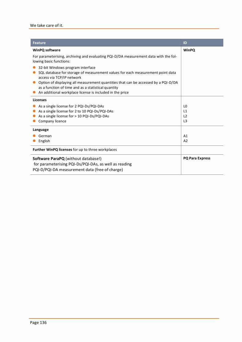
We take care of it.
Page 136
Feature ID
WinPQ software
For parameterising, archiving and evaluating PQI-D/DA measurement data with the fol-lowing basic functions:
0 32-bit Windows program interface 0 SQL database for storage of measurement values for each measurement point data
access via TCP/IP network
0 Option of displaying all measurement quantities that can be accessed by a PQI-D/DA as a function of time and as a statistical quantity
0 An additional workplace license is included in the price
WinPQ
Licenses
0 As a single license for 2 PQI-Ds/PQI-DAs
0 As a single license for 2 to 10 PQI-Ds/PQI-DAs 0 As a single license for > 10 PQI-Ds/PQI-DAs 0 Company licence
L0 L1
L2 L3
Language
0 German 0 English
A1 A2
Further WinPQ licenses for up to three workplaces
Software ParaPQ (without database!) for parameterising PQI-Ds/PQI-DAs, as well as reading
PQI-D/PQI-DA measurement data (free of charge)
PQ Para Express
Notes
Page 137
Notes
Power Quality Interface – PQI-D – 29/06/2021
A. Eberle GmbH & Co. KG
Frankenstraße 160
90461 Nuremberg, Germany
Tel.: +49 (0) 911 / 62 81 08-0
Fax: +49 (0) 911 / 62 81 08 96
E-mail: [email protected]
http://www.a-eberle.de
Software version:
_______________________________
Version: 130703
Version: 29.06.2021 11:11


![A New Paradigm for the Sociology of Knowledge [Eberle]](https://img.pdfslide.us/doc/110x75/577cbfc41a28aba7118e0a17/a-new-paradigm-for-the-sociology-of-knowledge-eberle.jpg)