Embed Size (px)
Citation preview

© 2016 TSMC, Ltd
TSMC Property
GaN on Si ManufacturingExcellency in CMOS Foundry Fab
Paul ChuOct. 2016

© 2016 TSMC, Ltd
TSMC Property
1. GaN Device Offering2. GaN Production
3. GaN MoCVD Manufacturability4. Yield Improvement 5. Summary
Agenda

© 2016 TSMC, Ltd
2
TSMC PropertyGaN device offering
l GaN superiority
l Good efficiency on system operation

© 2016 TSMC, Ltd
3
TSMC PropertyGaN device offering
650V
100V
40V
E-HEMT D-MIS D-HEMT
Ready
Technology Function Application650V E-HEMT AC-DC, DC-AC Adaptor, Motor controller, PV inverter650V D-MIS AC-DC, DC-AC Adaptor, Motor controller, PV inverter100V E-HEMT DC-DC IBC, Server, Notebook100V D-HEMT RF-PA WiFi, Base station40V D-MIS RF-switch WiFi, Base station
l GaN production since 2015l Engaged 15 customers/ 53 NTOl >90% of GaN common tools are shared with CMOS
manufacturing
© 2016 TSMC, Ltd
4
TSMC Property
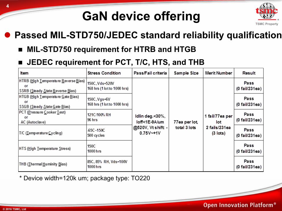
l Passed MIL-STD750/JEDEC standard reliability qualification n MIL-STD750 requirement for HTRB and HTGBn JEDEC requirement for PCT, T/C, HTS, and THB
GaN device offering
* Device width=120k um; package type: TO220

© 2016 TSMC, Ltd
5
TSMC PropertyProduction in tsmc
Total Clean Room Space (m2)C/R area: 9,800 m2
Technology Capability0.45um/0.5um/0.6um/0.8um/1.0um/1.2um/2.0um/3.0um
Lithographyi-line stepper, DUV stepper
6” Fab Key Milestones • 3.0um/1.2um/1.0um production 1990• 0.8um production 1992• 0.6um production 1994• 0.5um/0.45um production 1995• 1.0/0.6/0.5um HV production 2001• 0.6um BCD production 2006• 1.0/0.5um MEMS production 2007• GaN R&D 2011 • GaN production 2015

© 2016 TSMC, Ltd
6
TSMC Property
l Complex epitaxy GaN depositionl Warpage/Fragile wafer handlingl 1.5X thick substrate l Ultra thick metal l CMOS compatible metallization l Contamination control
Production Challenges

© 2016 TSMC, Ltd
7
TSMC Property
Gra
vity
Time
Gra
vity
Time
l Minimize vibration during transportation and process GaN Production
Vibration sensor
Action
before action after action
• Wafer transportation• Thermal ramp/cool rate optimization
• Hardware spec tighten
CMOS
GaN Wafer Broken Rate Trend
n Wireless n Real time monitor

© 2016 TSMC, Ltd
8
TSMC Property
l >90% common tools with CMOS
GaN Production
Comparable device process defect

© 2016 TSMC, Ltd
9
TSMC PropertyGaN Production
l GaN didn’t contaminate CMOS process
CMOS line stability

© 2016 TSMC, Ltd
10
TSMC Property
l 100% of WAT & In-line items passed production Cpkcriteria (Cpk > 1.33)
GaN Production
WAT & In-line Cpk

© 2016 TSMC, Ltd
11
TSMC PropertyGaN Production
l Comparable contact Rc with Au based metallization
Ref.-A: Low-resistance and high-reflectance Ni/Ag/Ru/Ni/Au ohmic contact on p-type GaN, APPLIED PHYSICS LETTERS VOLUME 85, NUMBER 19 8 NOVEMBER 2004
Ref.-B: Electrical, thermal, and microstructural characteristics of Ti/Al/Ti/Au multilayer Ohmic contacts to n-type GaN J. Appl. Phys. 93, 1087 (2003)
tsmc (Al base)
Ref. A (Au)Ref.-B (Au)
Al base Ohmic contact metallization
• Metal scheme• Process control

© 2016 TSMC, Ltd
12
TSMC Property
l Al based gate metallization with low gate leakage and wider Vg operation range. n Interface controln Electrical field optimization
l Offer Vg=7V operation (2016/Q4)
Production in tsmcIg
(mA
/mm
)Lo
g-sc
ale
specConsumer parts
tsmc parts
Vg-Ig Curve

© 2016 TSMC, Ltd
13
TSMC Property
l Excellent Cycle Time
GaN Production
(1) Tool stability improvement(2) Bottleneck capacity expansion(3) 2nd tool release
Time
GaN Cycle Time Improvement

© 2016 TSMC, Ltd
14
TSMC PropertyGaN MoCVD Production
LED Power Device
Issue: 1. Quantum efficiency2. Light extraction
Challenges: 1. Particle2. Wafer bow3. Dislocation density
Similar scheme w/i different challenges/requirements
Particle
© 2016 TSMC, Ltd
15
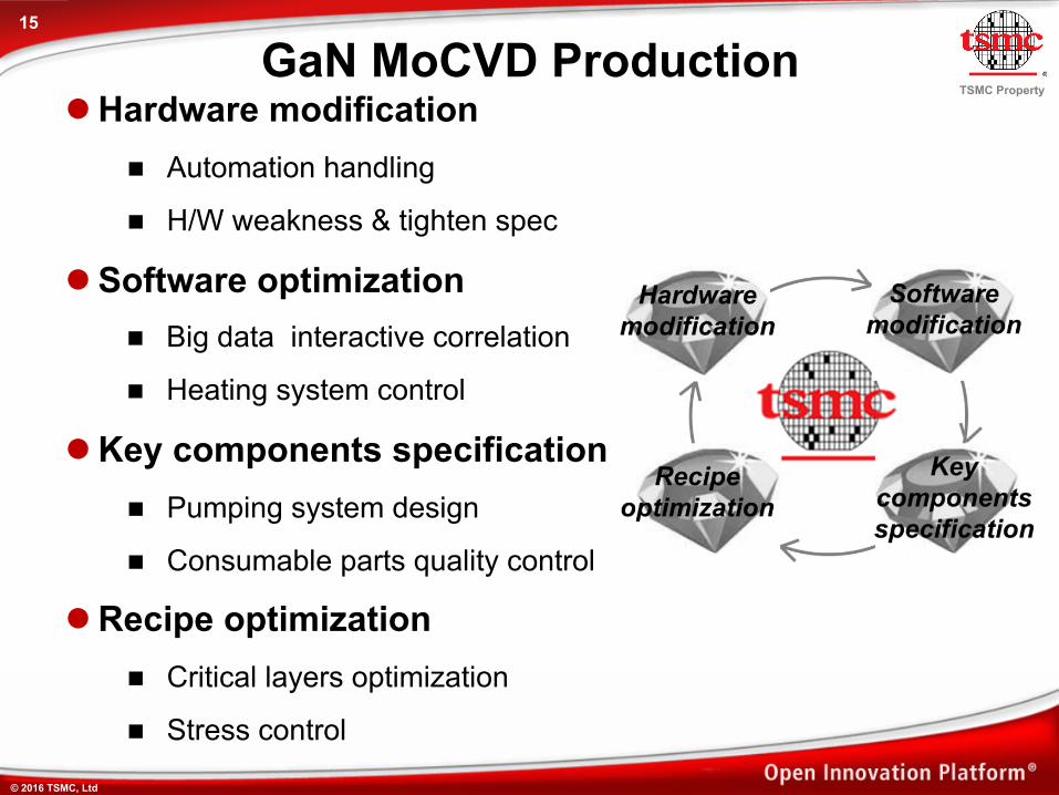
TSMC PropertyGaN MoCVD Production
lHardware modificationn Automation handling
n H/W weakness & tighten spec
lSoftware optimizationn Big data interactive correlation
n Heating system control
lKey components specification n Pumping system design
n Consumable parts quality control
lRecipe optimizationn Critical layers optimization
n Stress control

© 2016 TSMC, Ltd
16
TSMC PropertyGaN MoCVD Production
Characterization TechniquelNon-destructive
n Crystal quality: HR X-ray diffraction
n Wafer bow: In-situ monitor curvature, Ex-situ optical measurement
n Surface inspection: Candela optical metrology
lDestructiven AFM: Surface morphology
n SIMS: Profile of composition, impurity concentration
n TEM: Interface quality, dislocation density

© 2016 TSMC, Ltd
17
TSMC PropertyFault Detection and Classification
l The analysis of process data taken during a process run to
determine:n If the process is running normally or not (i.e. is a fault detected)
n The classification of faults for their source or cause
lPrevent excursion events by early detecting and warning
l Fault classification enables automatic fault identification

© 2016 TSMC, Ltd
18
TSMC PropertyiEDA (Interactive Engineering Data Analysis)
l SAS/graphic statistical software l Easy access, URD & IT skills not required> 90% reporting time saving
l Data access> 10X data access speed
l Wafer map correlation > Days to hours CP yield analysis

© 2016 TSMC, Ltd
19
TSMC PropertyParticle Control
Particle define
Candela(Distribution)
PFAanalysis
SEM(Type)
lParticle control with FDC and iEDA systemStep1: Wafer handling
Step2: Chamber Condition control
Step3: Particle excursiondetection
ü SPC excursion
Step4: Good –to-badlot comparison
Step5: H/W excursiondetection
Good
Bad
ü FDC correlation
Baseline improvement
© 2016 TSMC, Ltd
20
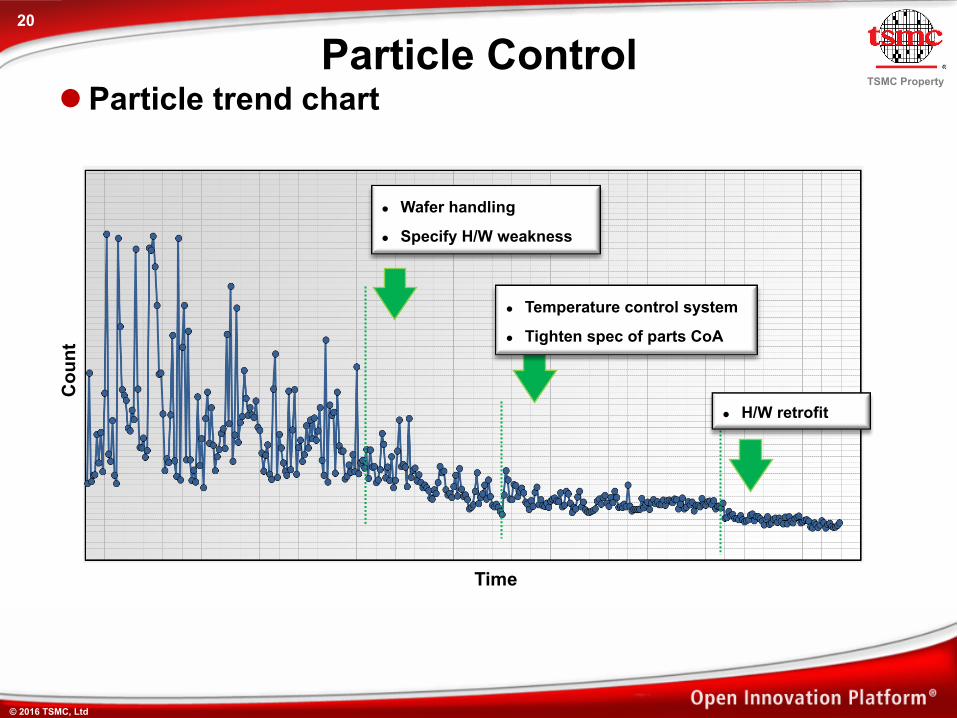
TSMC PropertyParticle Control
lParticle trend chartC
ount
Time
l Temperature control system
l Tighten spec of parts CoA
l Wafer handling
l Specify H/W weakness
l H/W retrofit

© 2016 TSMC, Ltd
21
TSMC PropertyWafer Bow Control
lBow control with FDC and iEDA systemStep1: FDC & SPC empowered by in-situ metrology
Step2: Good –to-badlot comparison
Step3: Tighten key parameters control
Step4: Recipe structureoptimization
ü Critical layer optimization

© 2016 TSMC, Ltd
22
TSMC PropertyWafer bow Control
lWafer bow trend chartC
ount
Time
l Recipe optimization
l Tighten temperature +
pressure + flow spec

© 2016 TSMC, Ltd
23
TSMC PropertyDislocation Density
lCritical layers optimization

© 2016 TSMC, Ltd
24
TSMC PropertyMatching Method
l Tool Matching by TSMC report functionStep1: FAC / Hardware matching
Step2: Critical Parts COA Matching
Step3: Software/ Recipe matching
Step4: SPC Matching
Step5: WAT/Cp yield Matching
PRS Match Function
Matching Result
COA Dashboard
Matching Result Matching Result
Defense All in One SPC Matching System One click Report
Matching Result Matching Result
Input Control Output Matching

© 2016 TSMC, Ltd
25
TSMC Property
l MoCVD GaN on Si multi layers epitaxy more than several thousands parameters collected for yield analysis
l Leveraged CMOS iEDA system for quick yield learning
Yield ImprovementC
P Yi
eld
1. FDC traces all EPI information 2. Intelligent EDA finds key process index 3. Well process control from CMOS learning4. Quick detection and corrective action. Process factors
Yiel
d fa
ilure
bin

© 2016 TSMC, Ltd
26
TSMC Property
l EPI electrical quality early detection methodology, Cycle time is improved from xx days to 1 day.
l Speed up the learning curve of EPI yield improvement
Yield Improvement
Yield correlation

© 2016 TSMC, Ltd
27
TSMC Property
l GaN on Si production launched since 2015 with good cycle time, yield and performance
l The most advanced CMOS manufacture process control and yield enhancement systems are adopted.
l Customer/tsmc/OSAT supply chain collaboration are critical for product grade
l Continuously performance enhancement and cost reduction to stay ahead of competition.
Summary