Embed Size (px)
Citation preview
1 QorvoTM Confidential & Proprietary Information
© 2015 Qorvo, Inc.
QorvoTM Confidential & Proprietary Information
© 2015 Qorvo, Inc.
Gallium Nitride Power MMICs – Fact and Fiction Charles F. Campbell

2 QorvoTM Confidential & Proprietary Information
© 2015 Qorvo, Inc.
Gallium Nitride has many attractive characteristics
• High operating voltage capability (VBD )
• High current capability (IMAX )
• Good microwave performance (GMAX , fT , fMAX )
• Good low noise performance (NFMIN )
• High thermal conductivity Silicon Carbide substrate
Should be ideal for microwave power applications!
Introduction
3 QorvoTM Confidential & Proprietary Information
© 2015 Qorvo, Inc.
Use of GaN based technology is rapidly growing
• Military (Radar, EW, Communications)
• Infrastructure (Basestation, Weather Radar, Satcom)
• Commercial (CATV, Test equipment)
Numerous circuit functions have been demonstrated
• Power amplifiers
• Low noise amplifiers
• RF control components
Introduction
4 QorvoTM Confidential & Proprietary Information
© 2015 Qorvo, Inc.
GaN MMIC design however is not without issues
Some are obvious
• High voltage / high current
• Thermal
Some are less so
• Wideband power amplifier designs
• Power combining
• User interface / driver circuitry
Introduction
5 QorvoTM Confidential & Proprietary Information
© 2015 Qorvo, Inc.
High voltage operation = higher output impedance
• Reduced transformation ratios
• Lower loss, wider band matching networks
• Less complex combining networks or more power
All true! Sometimes …….
• Narrow to moderate bandwidth designs do benefit
• Low frequency wideband designs also benefit
High Output Impedance = More Bandwidth?
6 QorvoTM Confidential & Proprietary Information
© 2015 Qorvo, Inc.
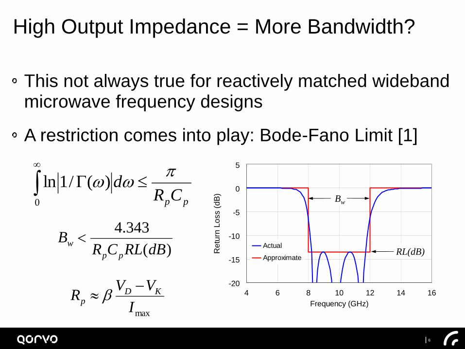
This not always true for reactively matched wideband microwave frequency designs
A restriction comes into play: Bode-Fano Limit [1]
High Output Impedance = More Bandwidth?
0
)(/1lnppCR
d
4 6 8 10 12 14 16
Frequency (GHz)
-20
-15
-10
-5
0
5
Re
turn
Lo
ss (
dB
)
Actual
Approximate
Bw
RL(dB))(
343.4
dBRLCRB
pp
w
maxI
VVR KD
p
7 QorvoTM Confidential & Proprietary Information
© 2015 Qorvo, Inc.
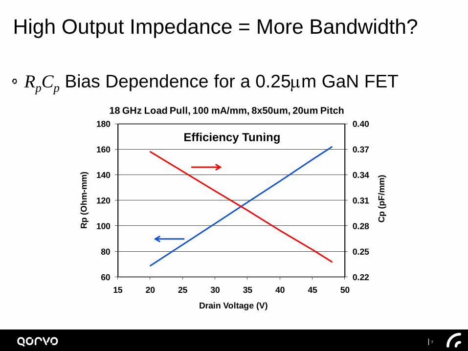
RpCp Bias Dependence for a 0.25mm GaN FET
High Output Impedance = More Bandwidth?
0.22
0.25
0.28
0.31
0.34
0.37
0.40
60
80
100
120
140
160
180
15 20 25 30 35 40 45 50
Cp
(p
F/m
m)
Rp
(O
hm
-mm
)
Drain Voltage (V)
18 GHz Load Pull, 100 mA/mm, 8x50um, 20um Pitch
Efficiency Tuning
8 QorvoTM Confidential & Proprietary Information
© 2015 Qorvo, Inc.
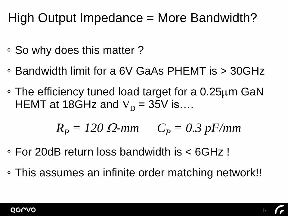
So why does this matter ?
Bandwidth limit for a 6V GaAs PHEMT is > 30GHz
The efficiency tuned load target for a 0.25mm GaN HEMT at 18GHz and VD = 35V is….
RP = 120 W-mm CP = 0.3 pF/mm
For 20dB return loss bandwidth is < 6GHz !
This assumes an infinite order matching network!!
High Output Impedance = More Bandwidth?

9 QorvoTM Confidential & Proprietary Information
© 2015 Qorvo, Inc.
Bandwidth increases if CP is reduced
Fundamental idea behind the distributed amplifier
Uniform distributed amplifier – Not a good PA
Dealing with Bode-Fano
RL
Zd
Q1
Zg
Cg
Zd
Q2
Zg
Cg
Zd
QN
Zg
Cg
RLgRFIN
Zd
Q3
Zg
Cg
RLd
10 QorvoTM Confidential & Proprietary Information
© 2015 Qorvo, Inc.
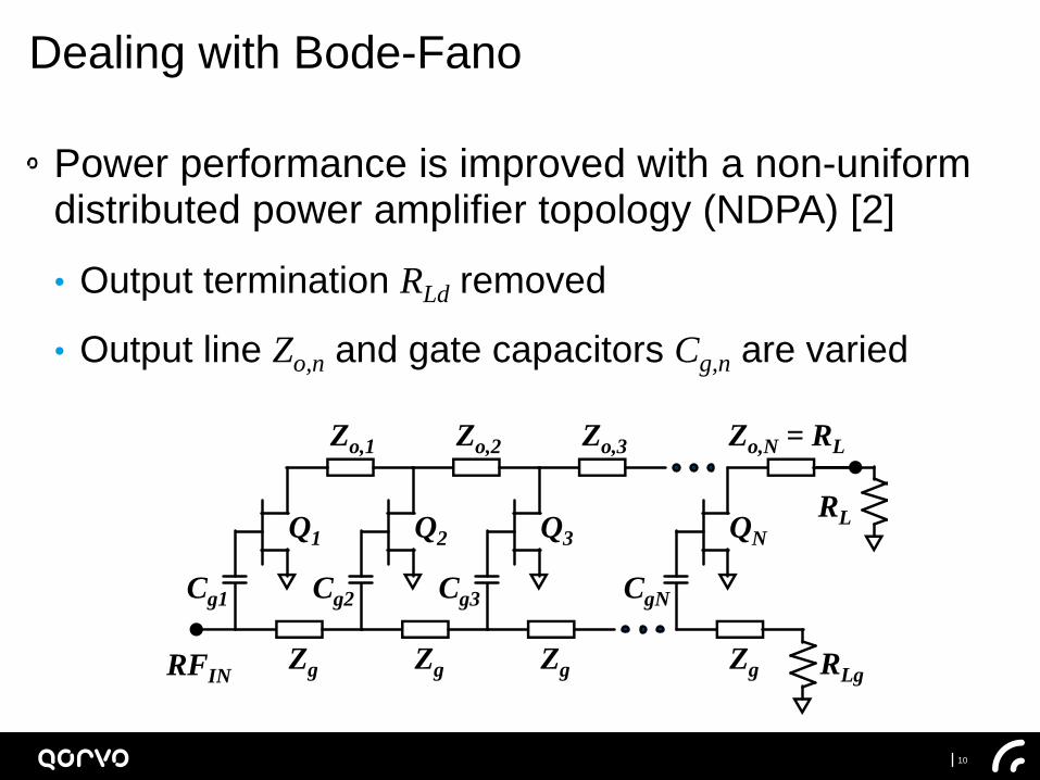
Power performance is improved with a non-uniform distributed power amplifier topology (NDPA) [2]
• Output termination RLd removed
• Output line Zo,n and gate capacitors Cg,n are varied
Dealing with Bode-Fano
RL
Zo,1
Q1
Zg
Cg1
Zo,2
Q2
Zg
Cg2
Zo,N = RL
QN
Zg
CgN
RLgRFIN
Zo,3
Q3
Zg
Cg3
11 QorvoTM Confidential & Proprietary Information
© 2015 Qorvo, Inc.
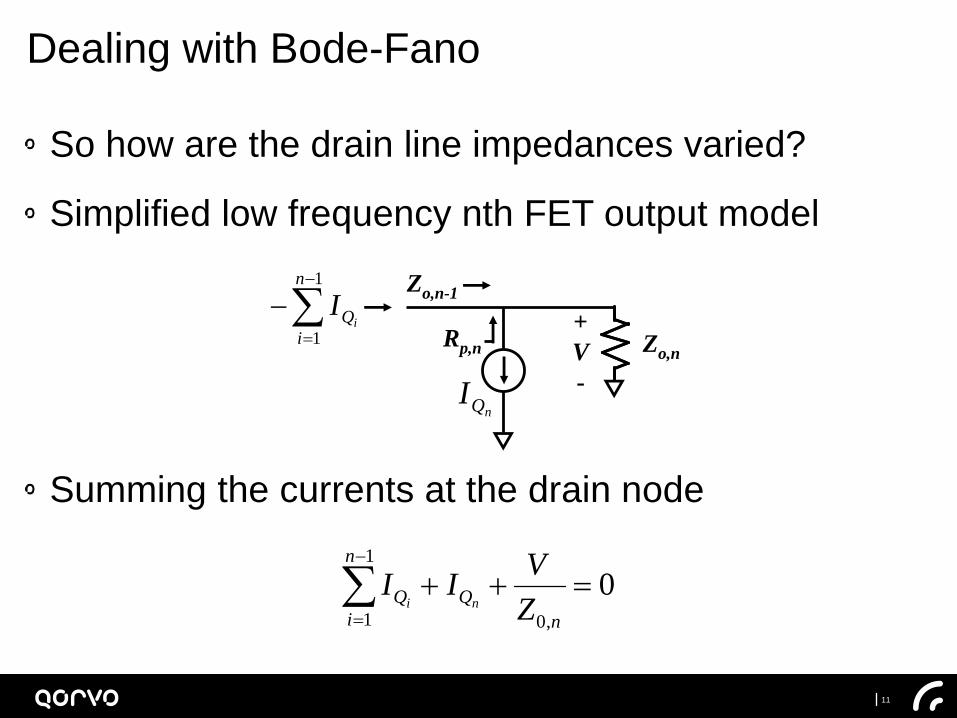
So how are the drain line impedances varied?
Simplified low frequency nth FET output model
Summing the currents at the drain node
Dealing with Bode-Fano
Rp,n
Zo,n-1
+
V
-
1
1
n
i
QiI
Zo,n
nQI
01
1 ,0
n
i n
QQZ
VII
ni
12 QorvoTM Confidential & Proprietary Information
© 2015 Qorvo, Inc.
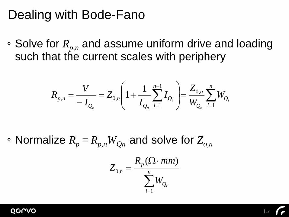
Solve for Rp,n and assume uniform drive and loading such that the current scales with periphery
Normalize Rp = Rp,nWQn and solve for Zo,n
Dealing with Bode-Fano
n
i
Q
Q
nn
i
Q
Q
n
Q
np i
n
i
nn
WW
ZI
IZ
I
VR
1
,01
1
,0,
11
W
n
i
Q
p
n
iW
mmRZ
1
,0
)(
13 QorvoTM Confidential & Proprietary Information
© 2015 Qorvo, Inc.
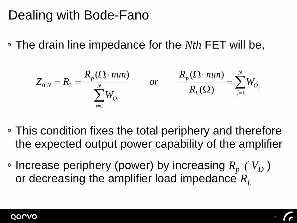
The drain line impedance for the Nth FET will be,
This condition fixes the total periphery and therefore the expected output power capability of the amplifier
Increase periphery (power) by increasing Rp ( VD ) or decreasing the amplifier load impedance RL
Dealing with Bode-Fano
W
WW
N
j
Q
L
p
N
i
Q
p
LN j
i
WR
mmRor
W
mmRRZ
1
1
,0)(
)()(

14 QorvoTM Confidential & Proprietary Information
© 2015 Qorvo, Inc.
Consider the following example for RL = 50W
• N = 10 FET cells
• RP =120 W-mm
• Total Periphery: 2.4mm
• Power: 7-12W (3-5W/mm)
Very high Zo
Q1 size sets max Zo [3]
The first transistors are poorly loaded!
Dealing with Bode-Fano
0
100
200
300
400
500
600
0 1 2 3 4 5 6 7 8 9 10 11
Dra
in L
ine
Imp
edan
ce (
Oh
m)
Transistor Cell
Q1-Q10 = 240um
Q1=600um, Q2-Q10=200um
Maximum
Realizable Zo on
100um Thick SiC
15 QorvoTM Confidential & Proprietary Information
© 2015 Qorvo, Inc.
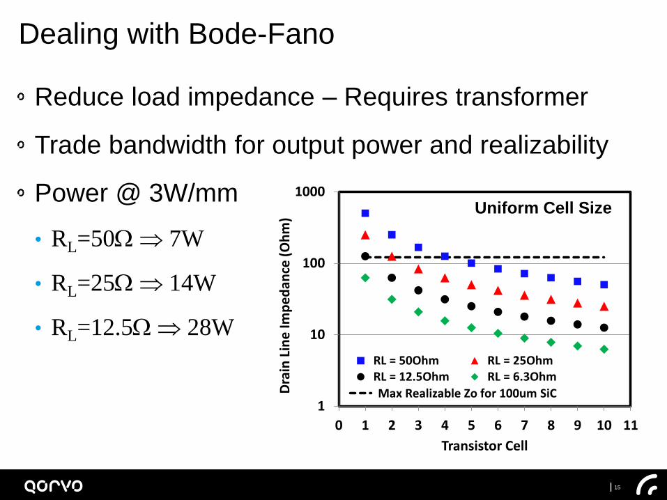
Reduce load impedance – Requires transformer
Trade bandwidth for output power and realizability
Power @ 3W/mm
• RL=50W 7W
• RL=25W 14W
• RL=12.5W 28W
Dealing with Bode-Fano
1
10
100
1000
0 1 2 3 4 5 6 7 8 9 10 11
Dra
in L
ine
Imp
ed
ance
(O
hm
)
Transistor Cell
RL = 50Ohm RL = 25OhmRL = 12.5Ohm RL = 6.3Ohm
Max Realizable Zo for 100um SiC
Uniform Cell Size
16 QorvoTM Confidential & Proprietary Information
© 2015 Qorvo, Inc.
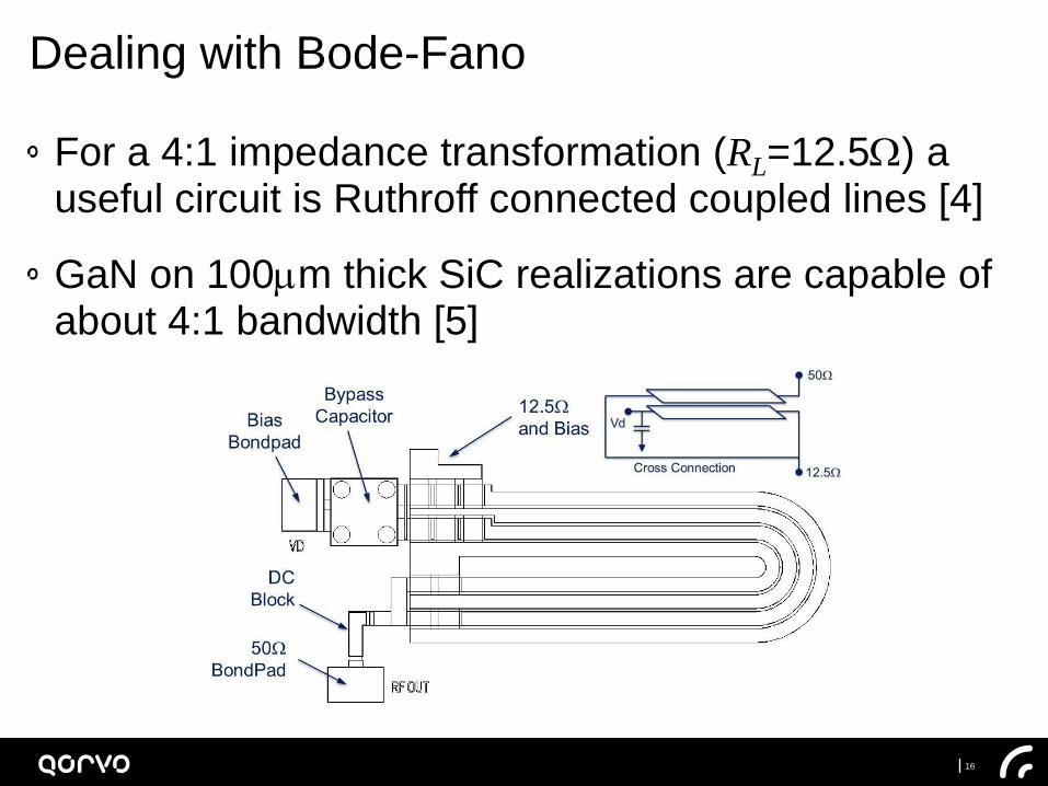
For a 4:1 impedance transformation (RL=12.5W) a useful circuit is Ruthroff connected coupled lines [4]
GaN on 100mm thick SiC realizations are capable of about 4:1 bandwidth [5]
Dealing with Bode-Fano
17 QorvoTM Confidential & Proprietary Information
© 2015 Qorvo, Inc.
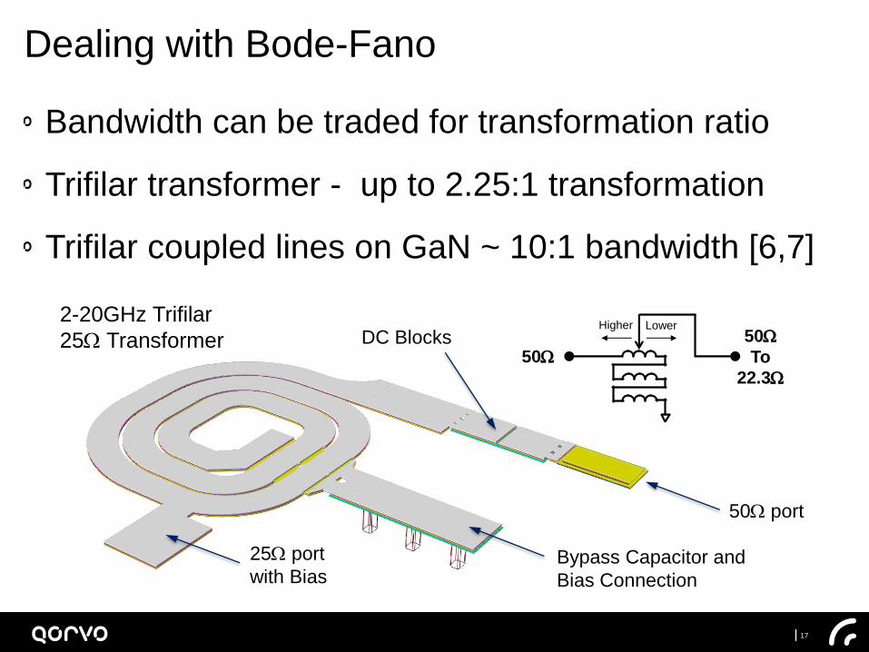
Bandwidth can be traded for transformation ratio
Trifilar transformer - up to 2.25:1 transformation
Trifilar coupled lines on GaN ~ 10:1 bandwidth [6,7]
Dealing with Bode-Fano
50W
50W
To
22.3W
Higher Lower
25W port
with Bias
DC Blocks
Bypass Capacitor and
Bias Connection
50W port
2-20GHz Trifilar
25W Transformer
18 QorvoTM Confidential & Proprietary Information
© 2015 Qorvo, Inc.
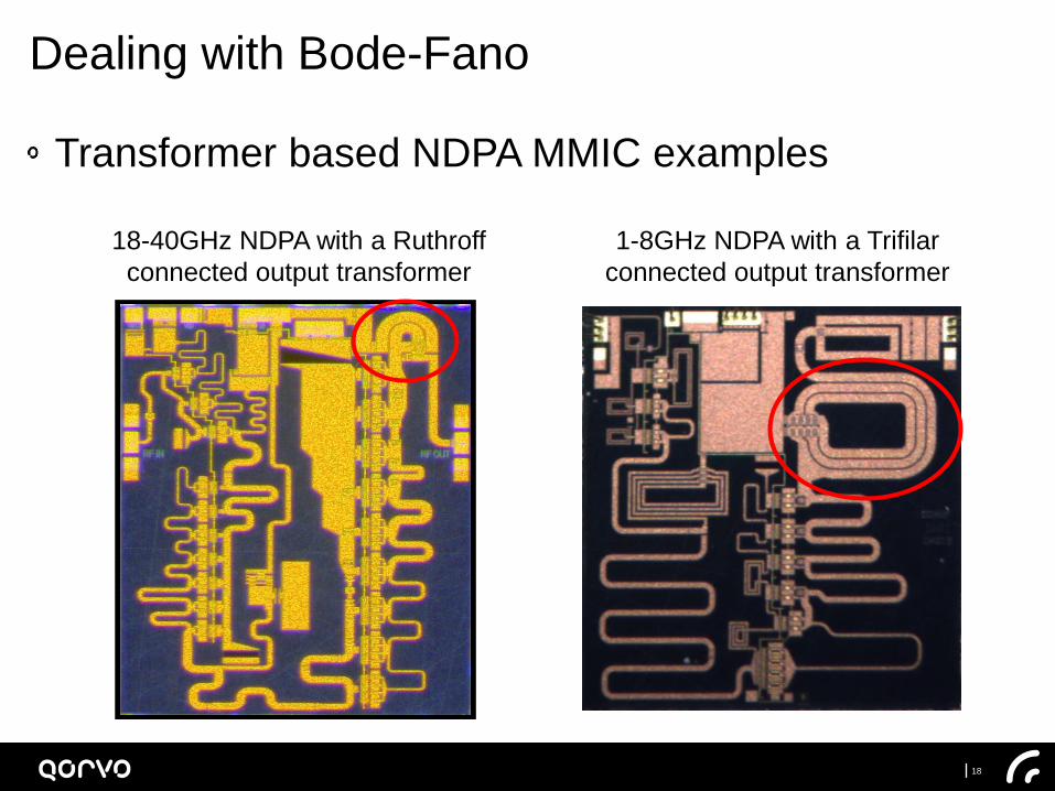
Transformer based NDPA MMIC examples
Dealing with Bode-Fano
18-40GHz NDPA with a Ruthroff
connected output transformer
1-8GHz NDPA with a Trifilar
connected output transformer
19 QorvoTM Confidential & Proprietary Information
© 2015 Qorvo, Inc.
Most GaN MMIC processes use SiC as a substrate
Thermal conductivity of SiC exceeds that of copper
Heat is transferred effectively to the back of the die
The power density of GaN HEMTs 3-5X higher than a GaAs PHEMT of equal periphery
The power added efficiency is however similar
The problem: 3-5X more heat flux to be removed
Why is My Part So Hot?
20 QorvoTM Confidential & Proprietary Information
© 2015 Qorvo, Inc.
Thermal management burden is placed on the user
Failure to remove heat Higher MMIC base temp
Today designers must practice thermal management
• Increase gate pitch Reduced RF performance
• Increase cell separation Die size and stability
• Individual source vias (ISVs) Die size
• Tune for Max PAE Reduced Power or linearity
Why is My Part So Hot?
21 QorvoTM Confidential & Proprietary Information
© 2015 Qorvo, Inc.
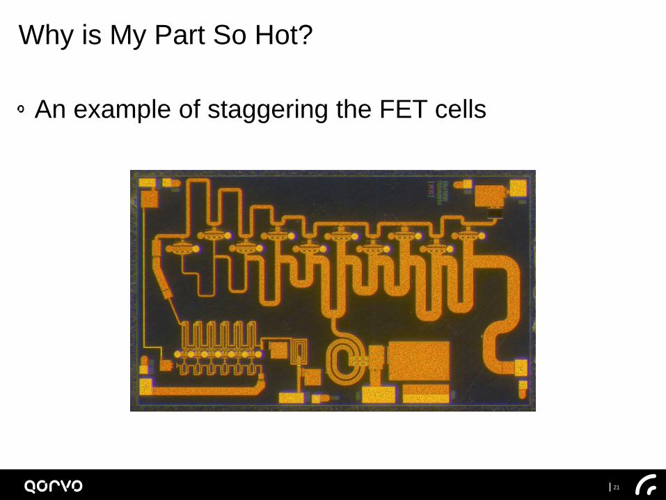
An example of staggering the FET cells
Why is My Part So Hot?
22 QorvoTM Confidential & Proprietary Information
© 2015 Qorvo, Inc.
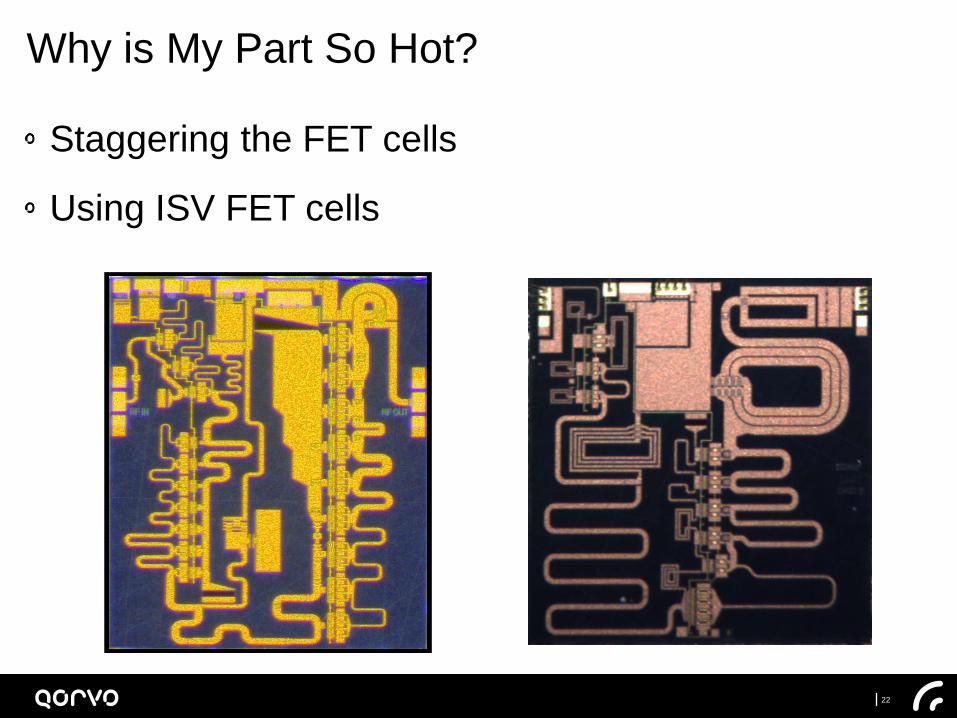
Staggering the FET cells
Using ISV FET cells
Why is My Part So Hot?

23 QorvoTM Confidential & Proprietary Information
© 2015 Qorvo, Inc.
An interesting example - power was reported power to be 1dB low for the 20mm FET die with loadpull prematch
An unexpected temperature distribution was noted
Why is My Part So Hot?
24 QorvoTM Confidential & Proprietary Information
© 2015 Qorvo, Inc.
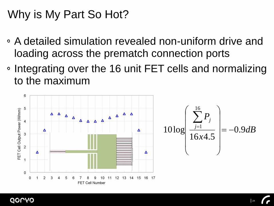
A detailed simulation revealed non-uniform drive and loading across the prematch connection ports
Integrating over the 16 unit FET cells and normalizing to the maximum
Why is My Part So Hot?
dBx
Pj
j
9.05.416
log10
16
1
25 QorvoTM Confidential & Proprietary Information
© 2015 Qorvo, Inc.
The odd temperature distribution for the 20mm FET is caused by asymmetries in the combining network
Some sources of combiner asymmetry
• Mutual inductance between parallel bond wires
• Mode formation due to curves and bends
• Coupling between microstrip lines
• Sharing source vias between adjacent cells
• Nonuniform temp. from adjacent cell heating
The Devil is in the Power Combining
26 QorvoTM Confidential & Proprietary Information
© 2015 Qorvo, Inc.
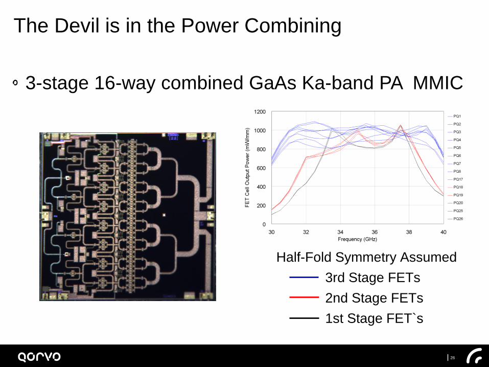
3-stage 16-way combined GaAs Ka-band PA MMIC
The Devil is in the Power Combining
Half-Fold Symmetry Assumed
3rd Stage FETs
2nd Stage FETs
1st Stage FET`s
27 QorvoTM Confidential & Proprietary Information
© 2015 Qorvo, Inc.
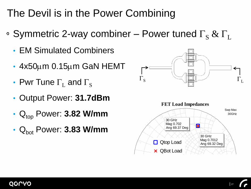
Symmetric 2-way combiner – Power tuned S & L
• EM Simulated Combiners
• 4x50mm 0.15mm GaN HEMT
• Pwr Tune L and S
• Output Power: 31.7dBm
• Qtop Power: 3.82 W/mm
• Qbot Power: 3.83 W/mm
The Devil is in the Power Combining
0 1.0
1.0
-1.0
10.0
10.0
-10.0
5.0
5.0
-5.0
2.0
2.0
-2.0
3.0
3.0
-3.0
4.0
4.0
-4.0
0.2
0.2
-0.2
0.4
0.4
-0.4
0.6
0.6
-0.6
0.8
0.8
-0.8
FET Load ImpedancesSwp Max
30GHz
Swp Min
30GHz
30 GHzMag 0.702Ang 69.37 Deg
30 GHzMag 0.7012Ang 69.32 DegQtop Load
QBot Load
S L
28 QorvoTM Confidential & Proprietary Information
© 2015 Qorvo, Inc.
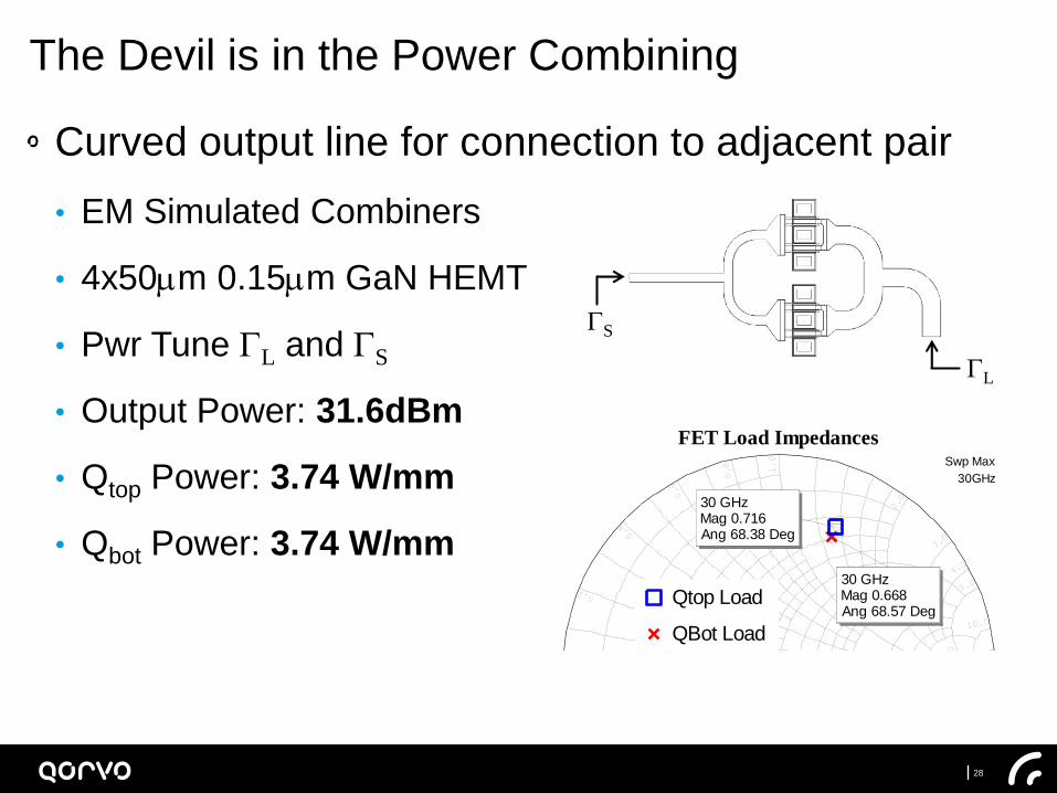
Curved output line for connection to adjacent pair
• EM Simulated Combiners
• 4x50mm 0.15mm GaN HEMT
• Pwr Tune L and S
• Output Power: 31.6dBm
• Qtop Power: 3.74 W/mm
• Qbot Power: 3.74 W/mm
The Devil is in the Power Combining
S
L
0 1.0
1.0
-1.0
10.0
10.0
-10.0
5.0
5.0
-5.0
2.0
2.0
-2.0
3.0
3.0
-3.0
4.0
4.0
-4.0
0.2
0.2
-0.2
0.4
0.4
-0.4
0.6
0.6
-0.6
0.8
0.8
-0.8
FET Load ImpedancesSwp Max
30GHz
Swp Min
30GHz
30 GHzMag 0.716Ang 68.38 Deg
30 GHzMag 0.668Ang 68.57 Deg
Qtop Load
QBot Load
29 QorvoTM Confidential & Proprietary Information
© 2015 Qorvo, Inc.
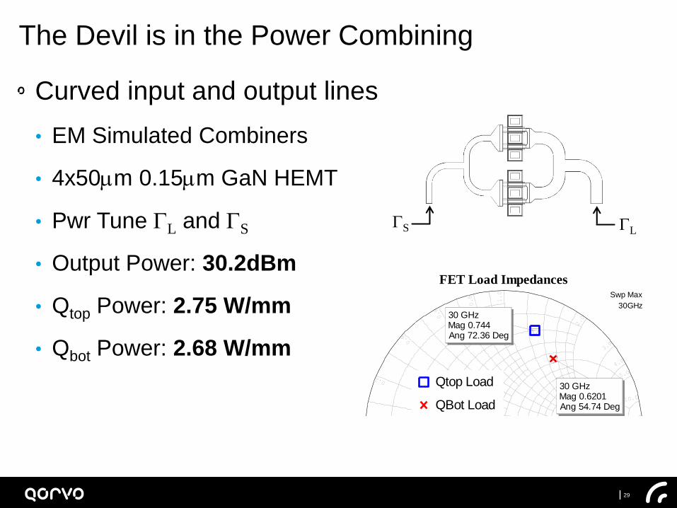
Curved input and output lines
• EM Simulated Combiners
• 4x50mm 0.15mm GaN HEMT
• Pwr Tune L and S
• Output Power: 30.2dBm
• Qtop Power: 2.75 W/mm
• Qbot Power: 2.68 W/mm
The Devil is in the Power Combining
0 1.0
1.0
-1.0
10.0
10.0
-10.0
5.0
5.0
-5.0
2.0
2.0
-2.0
3.0
3.0
-3.0
4.0
4.0
-4.0
0.2
0.2
-0.2
0.4
0.4
-0.4
0.6
0.6
-0.6
0.8
0.8
-0.8
FET Load ImpedancesSwp Max
30GHz
Swp Min
30GHz
30 GHzMag 0.744Ang 72.36 Deg
30 GHzMag 0.6201Ang 54.74 Deg
Qtop Load
QBot Load
S L
30 QorvoTM Confidential & Proprietary Information
© 2015 Qorvo, Inc.
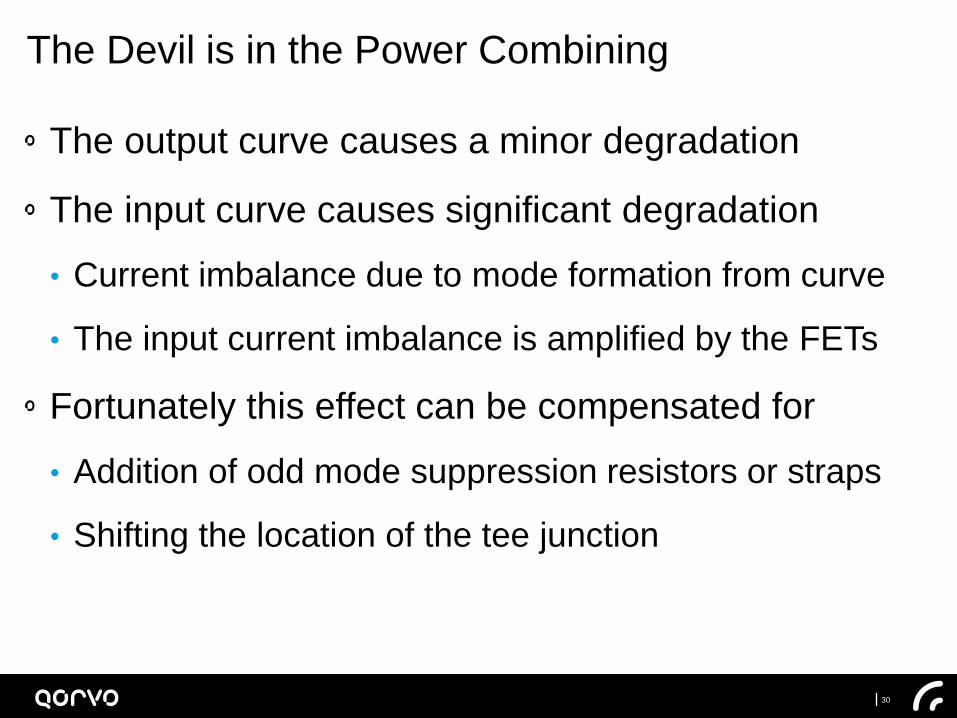
The output curve causes a minor degradation
The input curve causes significant degradation
• Current imbalance due to mode formation from curve
• The input current imbalance is amplified by the FETs
Fortunately this effect can be compensated for
• Addition of odd mode suppression resistors or straps
• Shifting the location of the tee junction
The Devil is in the Power Combining

31 QorvoTM Confidential & Proprietary Information
© 2015 Qorvo, Inc.
Compensated curved input and output lines
• Add Odd Mode Resistors
• Offset Tee Junctions
• Pwr Tune L and S
• Output Power: 31.7dBm
• Qtop Power: 3.86 W/mm
• Qbot Power: 3.78 W/mm
The Devil is in the Power Combining
S L
0 1.0
1.0
-1.0
10.0
10.0
-10.0
5.0
5.0
-5.0
2.0
2.0
-2.0
3.0
3.0
-3.0
4.0
4.0
-4.0
0.2
0.2
-0.2
0.4
0.4
-0.4
0.6
0.6
-0.6
0.8
0.8
-0.8
FET Load ImpedancesSwp Max
30GHz
Swp Min
30GHz
30 GHzMag 0.7Ang 69.47 Deg
30 GHzMag 0.7029Ang 68.88 DegQtop Load
QBot Load
32 QorvoTM Confidential & Proprietary Information
© 2015 Qorvo, Inc.
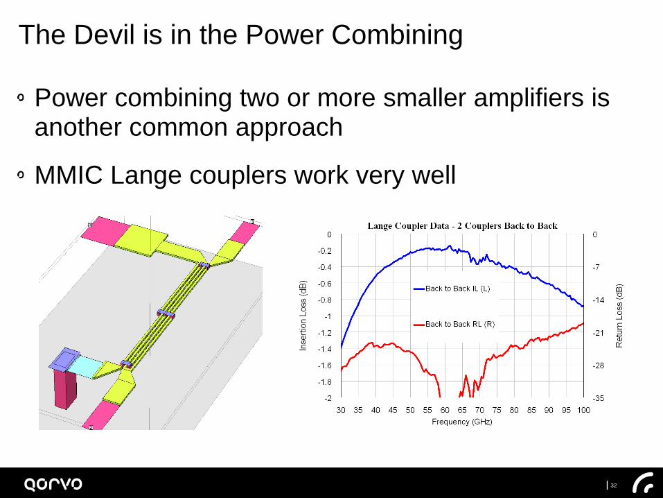
Power combining two or more smaller amplifiers is another common approach
MMIC Lange couplers work very well
The Devil is in the Power Combining
33 QorvoTM Confidential & Proprietary Information
© 2015 Qorvo, Inc.
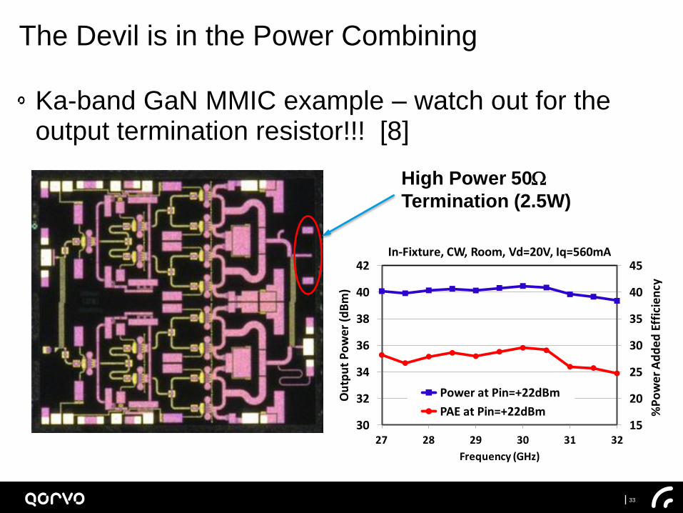
Ka-band GaN MMIC example – watch out for the output termination resistor!!! [8]
The Devil is in the Power Combining
High Power 50W
Termination (2.5W)
15
20
25
30
35
40
45
30
32
34
36
38
40
42
27 28 29 30 31 32
%P
ow
er
Ad
de
d E
ffic
ien
cy
Ou
tpu
t P
ow
er
(dB
m)
Frequency (GHz)
In-Fixture, CW, Room, Vd=20V, Iq=560mA
Power at Pin=+22dBm
PAE at Pin=+22dBm
34 QorvoTM Confidential & Proprietary Information
© 2015 Qorvo, Inc.
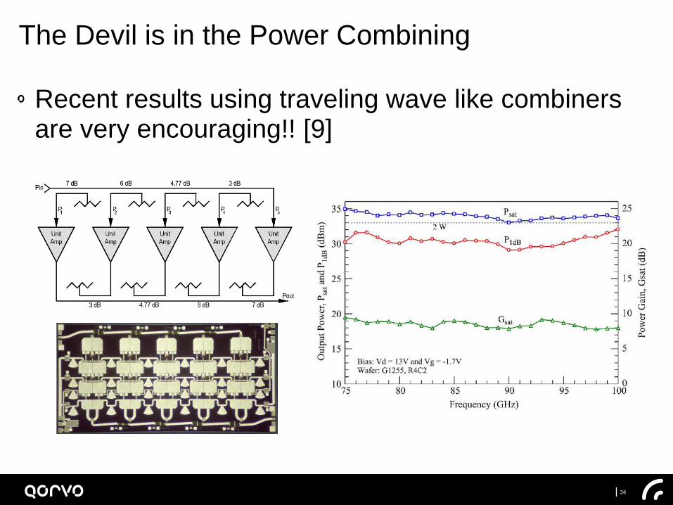
Recent results using traveling wave like combiners are very encouraging!! [9]
The Devil is in the Power Combining
35 QorvoTM Confidential & Proprietary Information
© 2015 Qorvo, Inc.
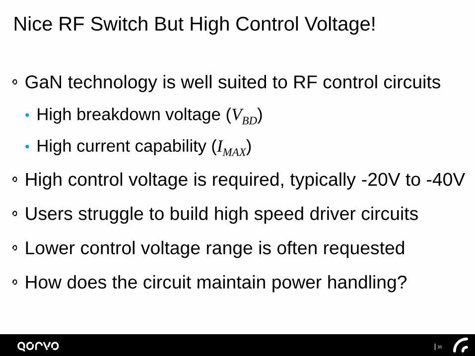
GaN technology is well suited to RF control circuits
• High breakdown voltage (VBD)
• High current capability (IMAX)
High control voltage is required, typically -20V to -40V
Users struggle to build high speed driver circuits
Lower control voltage range is often requested
How does the circuit maintain power handling?
Nice RF Switch But High Control Voltage!
36 QorvoTM Confidential & Proprietary Information
© 2015 Qorvo, Inc.
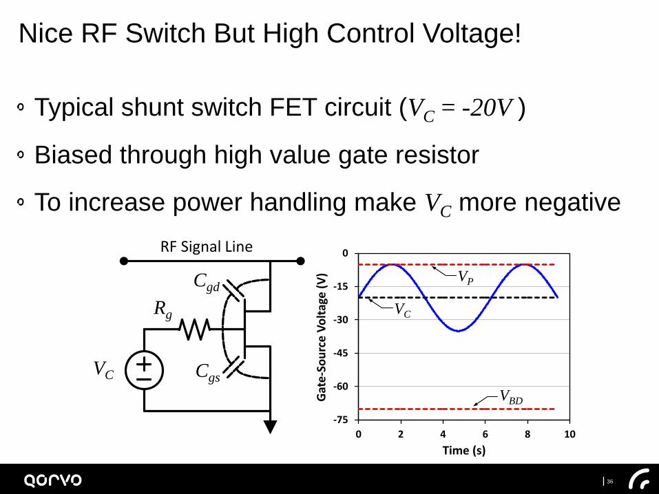
Typical shunt switch FET circuit (VC = -20V )
Biased through high value gate resistor
To increase power handling make VC more negative
Nice RF Switch But High Control Voltage!
Rg
VC
RF Signal Line
Cgd
Cgs
-75
-60
-45
-30
-15
0
0 2 4 6 8 10
Gat
e-S
ou
rce
Vo
ltag
e (
V)
Time (s)
VP
VC
VBD
37 QorvoTM Confidential & Proprietary Information
© 2015 Qorvo, Inc.
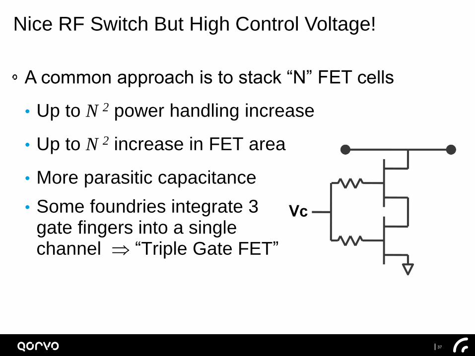
A common approach is to stack “N” FET cells
• Up to N 2 power handling increase
• Up to N 2 increase in FET area
• More parasitic capacitance
• Some foundries integrate 3 gate fingers into a single channel “Triple Gate FET”
Nice RF Switch But High Control Voltage!
38 QorvoTM Confidential & Proprietary Information
© 2015 Qorvo, Inc.
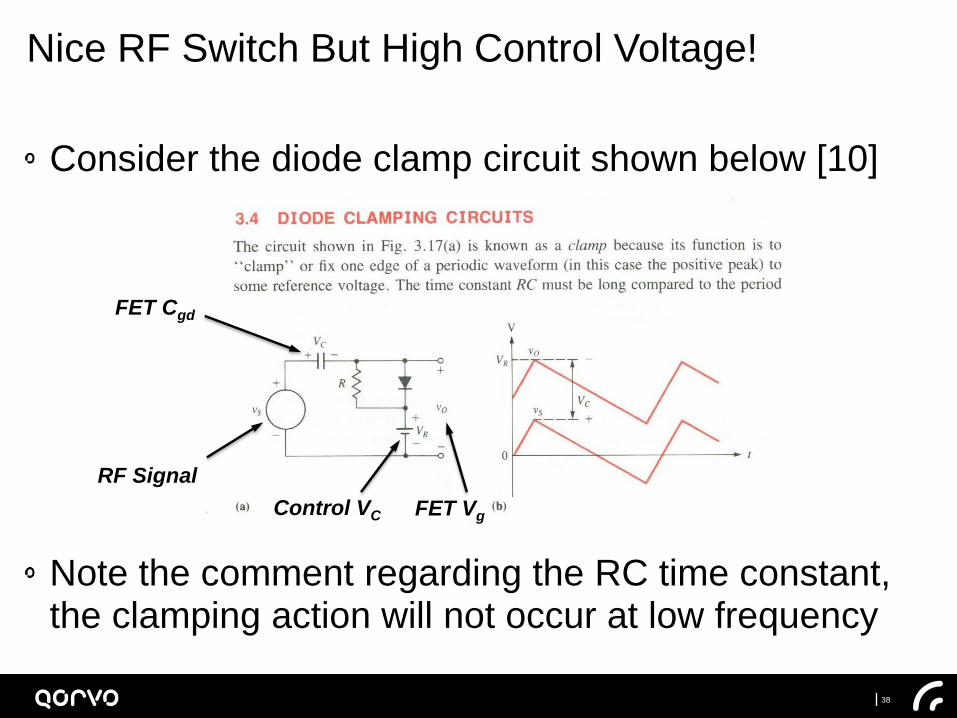
Consider the diode clamp circuit shown below [10]
Note the comment regarding the RC time constant, the clamping action will not occur at low frequency
Nice RF Switch But High Control Voltage!
RF Signal
FET Cgd
Control VC FET Vg
39 QorvoTM Confidential & Proprietary Information
© 2015 Qorvo, Inc.
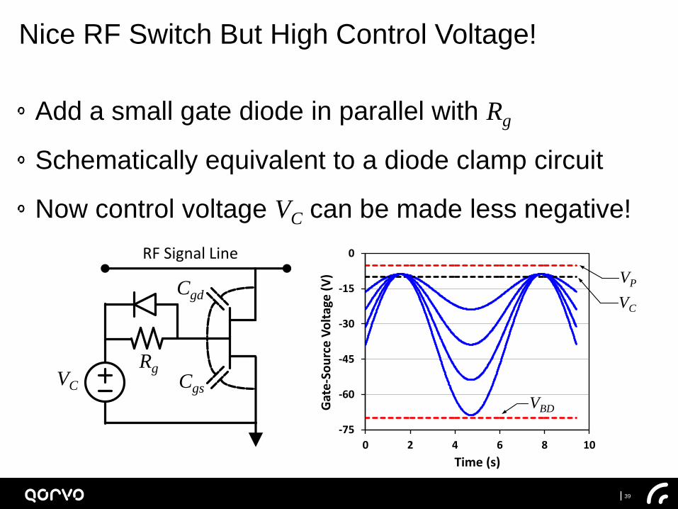
Add a small gate diode in parallel with Rg
Schematically equivalent to a diode clamp circuit
Now control voltage VC can be made less negative!
-75
-60
-45
-30
-15
0
0 2 4 6 8 10
Gat
e-S
ou
rce
Vo
ltag
e (
V)
Time (s)
VP
VC
VBD
VD
RgVC
RF Signal Line
Cgd
Cgs
Nice RF Switch But High Control Voltage!
-75
-60
-45
-30
-15
0
0 2 4 6 8 10
Gat
e-So
urc
e V
olt
age
(V)
Time (s)
VBD
VP
VC
40 QorvoTM Confidential & Proprietary Information
© 2015 Qorvo, Inc.
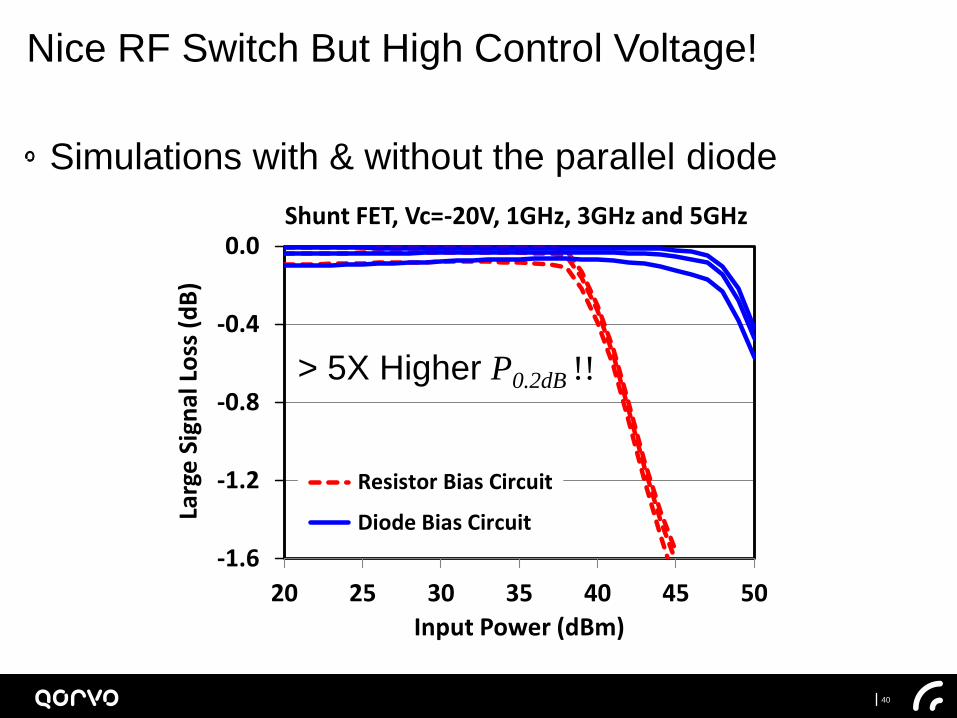
Simulations with & without the parallel diode
-1.6
-1.2
-0.8
-0.4
0.0
20 25 30 35 40 45 50
Larg
e S
ign
al L
oss
(d
B)
Input Power (dBm)
Shunt FET, Vc=-20V, 1GHz, 3GHz and 5GHz
Resistor Bias Circuit
Diode Bias Circuit
Nice RF Switch But High Control Voltage!
> 5X Higher P0.2dB !!
41 QorvoTM Confidential & Proprietary Information
© 2015 Qorvo, Inc.
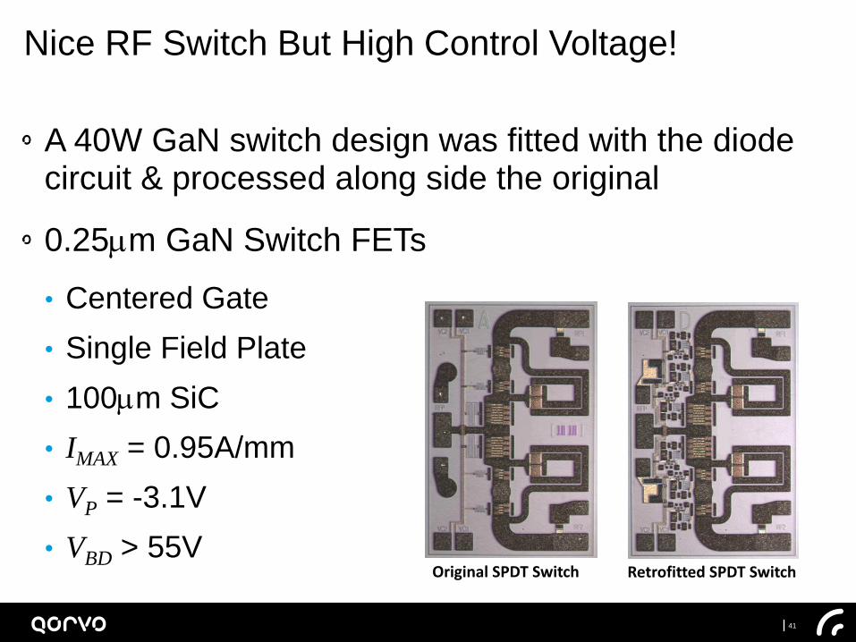
A 40W GaN switch design was fitted with the diode circuit & processed along side the original
0.25mm GaN Switch FETs
• Centered Gate
• Single Field Plate
• 100mm SiC
• IMAX = 0.95A/mm
• VP = -3.1V
• VBD > 55V
Original SPDT Switch Retrofitted SPDT Switch
Nice RF Switch But High Control Voltage!
42 QorvoTM Confidential & Proprietary Information
© 2015 Qorvo, Inc.
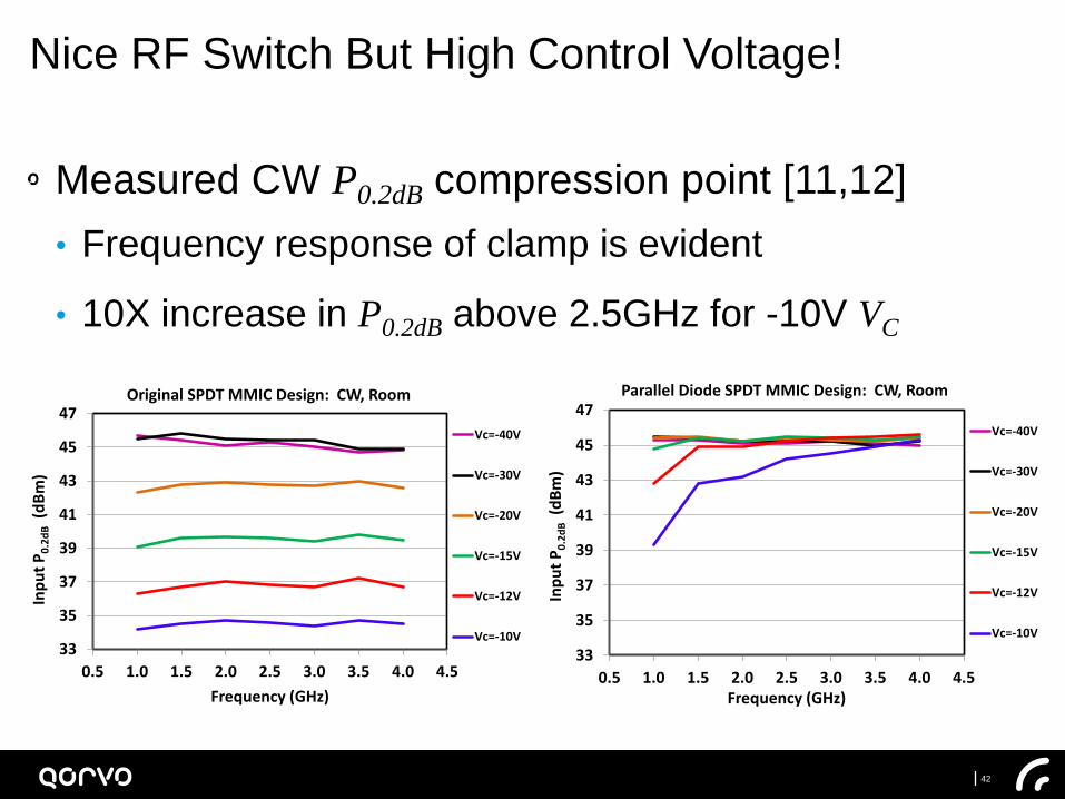
Measured CW P0.2dB compression point [11,12]
• Frequency response of clamp is evident
• 10X increase in P0.2dB above 2.5GHz for -10V VC
33
35
37
39
41
43
45
47
0.5 1.0 1.5 2.0 2.5 3.0 3.5 4.0 4.5
Inp
ut
P0
.2d
B(d
Bm
)
Frequency (GHz)
Original SPDT MMIC Design: CW, Room
Vc=-40V
Vc=-30V
Vc=-20V
Vc=-15V
Vc=-12V
Vc=-10V
33
35
37
39
41
43
45
47
0.5 1.0 1.5 2.0 2.5 3.0 3.5 4.0 4.5
Inp
ut
P0
.2d
B(d
Bm
)
Frequency (GHz)
Parallel Diode SPDT MMIC Design: CW, Room
Vc=-40V
Vc=-30V
Vc=-20V
Vc=-15V
Vc=-12V
Vc=-10V
Nice RF Switch But High Control Voltage!

43 QorvoTM Confidential & Proprietary Information
© 2015 Qorvo, Inc.
GaN MMIC technology is a real game changer
The enabling characteristics do come with issues
Hopefully this talk has illustrated some of the challenges associated with GaN MMIC design
Thank you for the opportunity to speak today!
Concluding Remarks
44 QorvoTM Confidential & Proprietary Information
© 2015 Qorvo, Inc.
[1] R. M. Fano, “Theoretical limitations on the broadband matching of arbitrary impedances,” J. Franklin Inst., vol. 249, pp. 57–83, 139–154, Jan./Feb. 1950.
[2] G. D. Vendelin, A. M. Pavio and U. L. Rohde, Microwave Circuit Design Using Linear and Nonlinear Techniques, John Wiley and Sons, 2005.
[3] C. Duperrier at al., “New Design Method of Uniform and Nonuniform Distributed Power Amplifiers”, IEEE Trans. Microw. Theory Techn., vol. 49, pp. 2494-2500, Dec. 2001.
[4] C. L. Ruthroff, "Some Broad-Band Transformers," Proceedings of the IRE , vol.47, no.8, pp.1337-1342, Aug. 1959.
[5] US Patent 8,988,161 “Transformer for Monolithic Microwave Integrated Circuits”
[6] J. Sevick, Transmission Line Transformers, Noble Pub. Corp. 4th Edition 2001.
[7] Patent Pending “Monolithic Wideband TriFilar Transformer”
[8] C. F. Campbell et al., “High efficiency Ka-band gallium nitride power amplifier MMICs,” 2013 IEEE Int. Microw. Comm., Antennas, Elect. Syst. Conf.
References
45 QorvoTM Confidential & Proprietary Information
© 2015 Qorvo, Inc.
[9] J. Schellenberg, “A 2-W W-Band GaN Traveling-Wave Amplifier With 25-GHz Bandwidth,” IEEE Trans. Microw. Theory Techn., vol. MTT-63, no. 9, pp. 2833– 2840, September 2015.
[10] S. G. Burns and P. R. Bond, Principles of Electronic Circuits, West Publishing Company, 1987.
[11] C. F. Campbell, “Method to Reduce Control Voltage for High Power GaN RF Switches”, IEEE MTT-S Int. Microwave Symp. Dig., 2015.
[12] Patent Pending “Bias Circuit for a High Power Radio Frequency Switching Device”
References