Embed Size (px)
Citation preview

Faculty of Electrical Engineering,Mathematics & Computer Science
Characterization of a Gallium NitrideHalf-Bridge module for use in a
Multi-Freqeuncy MultilevelModular Converter
Eelco BussinkB.Sc. ThesisAugust 2017
Supervisors:Moonen, D.J.G., M.Sc.
Leferink, prof.dr.ir.ing. F.B.J.Kokkeler, dr.ir. A.B.J.
Telecommunication Engineering GroupFaculty of Electrical Engineering,
Mathematics and Computer ScienceUniversity of Twente
P.O. Box 2177500 AE Enschede
The Netherlands
1
Summary
This reports shows measurements done on a gallium nitride half-bridge module, thesemeasurements will be the basis of EMI research of modules like this in a Multi-frequencyMultilevel Modular Converter (M3C) system, which will be a corner stone of a SmartGrid. Devices have to obey many rules and regulations to be Electromagnetic Com-patible (EMC), this makes versatility and controllability of signals within a device a mustin the design of such devices. This report gives some insight in the ringing effects onthe output with frequencies from 10 kHz up to 1 MHz, done with both the internal PWMgenerator and an FPGA as PWM input. Ringing can be a cause of ElectromagneticInterference (EMI). The FPGA is used to verify its capability for being used as an inputfor the GaN module, since the FPGA is easily programmable which results in easy ma-nipulation of signals. The ringing shows to be independent on frequency but dependenton dV
dt of the output. Furthermore the FPGA is capable of generating a PWM signal witha frequency of up to 1 MHz without introducing different ringing, showing a viable optionas input generator. At last some measurements with variable dead time are show whichare done with the FPGA. The variation in dead time has shown to be a viable way ofdecreasing overshoot at the output thus being able to influence EMI.
2

Keywords
Multi-frequency Multilevel Modular Converter (M3C)Gallium Nitride Half-BridgeRingingDead timeRise and Fall timeSmart Grid
3

Contents
1 Introduction 5
2 Theory 72.1 Ringing . . . . . . . . . . . . . . . . . . . . . . . . . . . . . . . . . . . . . 72.2 Rise and Fall time . . . . . . . . . . . . . . . . . . . . . . . . . . . . . . . 72.3 Duty Cycle . . . . . . . . . . . . . . . . . . . . . . . . . . . . . . . . . . . 82.4 Dead time . . . . . . . . . . . . . . . . . . . . . . . . . . . . . . . . . . . . 8
3 Analysis of the Modules 93.1 Motherboard (GS665EVBMB) . . . . . . . . . . . . . . . . . . . . . . . . . 93.2 GaN module (GS66504B) . . . . . . . . . . . . . . . . . . . . . . . . . . . 93.3 FPGA . . . . . . . . . . . . . . . . . . . . . . . . . . . . . . . . . . . . . . 103.4 Method of Measuring . . . . . . . . . . . . . . . . . . . . . . . . . . . . . . 10
4 Measurements 124.1 Measurements with internal PWM . . . . . . . . . . . . . . . . . . . . . . 124.2 Measurements with FPGA generated PWM input signals . . . . . . . . . 124.3 Comparison between the outputs with and without FPGA . . . . . . . . . 174.4 Measurements with load . . . . . . . . . . . . . . . . . . . . . . . . . . . . 174.5 Variation in deadtime . . . . . . . . . . . . . . . . . . . . . . . . . . . . . . 23
5 Evaluation Discussion 245.1 Conclusion . . . . . . . . . . . . . . . . . . . . . . . . . . . . . . . . . . . 245.2 Future research . . . . . . . . . . . . . . . . . . . . . . . . . . . . . . . . . 24
Appendix
4
1 Introduction
The so called ’Smart Grid’ is the upcoming term of the last few years. Research onSmart Grid is aimed at renewable energy, this includes a more efficient power transferfrom and towards the electrical grid. The current electrical grid is still governed by a50/60 Hz sinusoidal voltage, from a time where that was the only feasible way to transferpower. With the introduction of high power semiconductors, for instance Gallium Nitrideand Silicon Carbide, high voltage DC lines became realisable. GaN and SiC havethe advantage of being smaller and faster than Silicon based semiconductors. GaNdevices are grown on a standard silicon wafer whereas SiC needs a relatively expensivesubstrate [1].Both AC and DC systems have their advantages and disadvantages [2]. First a fewpros and cons for AC and DC systems will be reviewed and after that Multi-frequencyMultilevel Modular Converters (M3C) will be explained.
AC systems
Since the invention of electricity AC systems are the standard. This is because volt-age level conversion was only realisable via inductors, semiconductors had not beeninvented yet, thus only AC would work. This results in an immense amount of expe-rience and engineering practice combined with long standing protocols. The current50Hz 230V and 60Hz 110V grids, as standard and widely implemented, give easy im-plementable compatibility with regards to system design. The robustness on a largescale is achieved by interconnections and reserve generation, where as on small scalethe grid still relies on energy storage, predictive generation or load shedding especiallyin renewable energy systems.
DC systems
DC (micro)grids are becoming more realisable due to progress in power electronics bothin high voltage (HVDC) and low voltage (LVDC). Increase in renewable energy sources,such as solar, wind and thermal will benefit from HVDC systems due to simplicity andeconomic reasons [3]. There is an increasing number of consumer devices using DC,with an electrical grid that provides AC, results in most devices needing an AC-DCconverter which is a possible cost reduction if the grid would be DC. On the consumerlevel there is a huge increase in local renewables which usually output DC, like solarpanels and small windmills this increases complexity to transfer power to the grid. [4][5]
5
Multi-frequency Multilevel Modular Converters
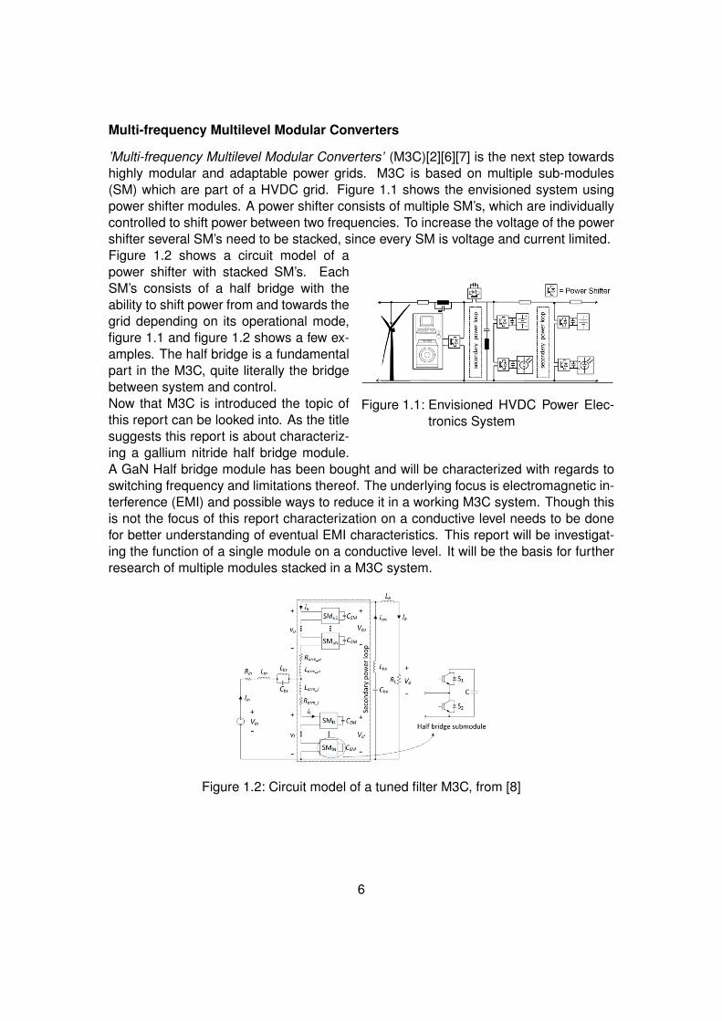
’Multi-frequency Multilevel Modular Converters’ (M3C)[2][6][7] is the next step towardshighly modular and adaptable power grids. M3C is based on multiple sub-modules(SM) which are part of a HVDC grid. Figure 1.1 shows the envisioned system usingpower shifter modules. A power shifter consists of multiple SM’s, which are individuallycontrolled to shift power between two frequencies. To increase the voltage of the powershifter several SM’s need to be stacked, since every SM is voltage and current limited.
Figure 1.1: Envisioned HVDC Power Elec-tronics System
Figure 1.2 shows a circuit model of apower shifter with stacked SM’s. EachSM’s consists of a half bridge with theability to shift power from and towards thegrid depending on its operational mode,figure 1.1 and figure 1.2 shows a few ex-amples. The half bridge is a fundamentalpart in the M3C, quite literally the bridgebetween system and control.Now that M3C is introduced the topic ofthis report can be looked into. As the titlesuggests this report is about characteriz-ing a gallium nitride half bridge module.A GaN Half bridge module has been bought and will be characterized with regards toswitching frequency and limitations thereof. The underlying focus is electromagnetic in-terference (EMI) and possible ways to reduce it in a working M3C system. Though thisis not the focus of this report characterization on a conductive level needs to be donefor better understanding of eventual EMI characteristics. This report will be investigat-ing the function of a single module on a conductive level. It will be the basis for furtherresearch of multiple modules stacked in a M3C system.
Figure 1.2: Circuit model of a tuned filter M3C, from [8]
6
2 Theory
This section will introduce a couple of definitions and theories on EMI. In the introduc-tion electromagnetic interference (EMI) has been mentioned. EMI describes the signalsthat cause interference from one device to another or from the environment to a device.An example of EMI generated by devices is a cellphone causing interference on an au-dio amplifier resulting in distorted sounds.The principle of electromagnetic compatibility (EMC) is both not producing or be sus-ceptible to interference. Since more and more devices are electrically controlled andsteered, rules and regulations have been put into place to ensure proper function of alldevices. Dependent on country or continent legislation EMC can vary.
Without going into detail about the legislation, insight in noise sources of devices isvital to be able to counter EMI. With regard to the GaN module there are four pointsof interest [9]. Since the output is a PWM signal, points of interest are ringing, rise/falltimes, duty cycle and dead time. The focus of will be on emission of the module.
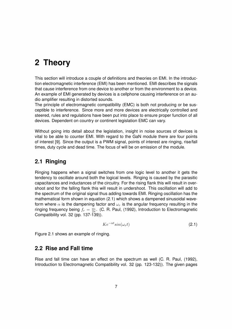
2.1 Ringing
Ringing happens when a signal switches from one logic level to another it gets thetendency to oscillate around both the logical levels. Ringing is caused by the parasiticcapacitances and inductances of the circuitry. For the rising flank this will result in over-shoot and for the falling flank this will result in undershoot. This oscillation will add tothe spectrum of the original signal thus adding towards EMI. Ringing oscillation has themathematical form shown in equation (2.1) which shows a dampened sinusoidal wave-form where α is the dampening factor and ωr is the angular frequency resulting in theringing frequency being fr = ωr
2π . (C. R. Paul, (1992), Introduction to ElectromagneticCompatibility vol. 32 (pp. 137-139)).
Ke−αtsin(ωrt) (2.1)
Figure 2.1 shows an example of ringing.
2.2 Rise and Fall time
Rise and fall time can have an effect on the spectrum as well (C. R. Paul, (1992),Introduction to Electromagnetic Compatibility vol. 32 (pp. 123-132)). The given pages
7
Figure 2.1: Example of ringing on a pulse signal, from [9]
show that for a pulse train a smaller (faster) rise and fall time give different spectralcontent than a larger (slower) rise and fall time.
2.3 Duty Cycle
Duty cycle is the percentage of time the PWM signal is on versus the signal being off,so 50% duty cycle means the PWM signal is turned on half of the period and turned offthe other half. In sinusoidal PWM varying the duty cycle is used to generated a PWMsignal that represents a sine wave when if filtered with a low pass filter, by rule of thumbthe carrier frequency should be about ten times higher than the original signal. It isnotable that in the situation of the half bridge configuration in this report a 50% dutycycle is practically impossible due to added dead time.
2.4 Dead time
Dead time is the time between switching on or off one transistor in a half bridge andturning off or on the other in said half bridge. This dead time is for safety so bothtransistors can never be on at the same time which would result in a short circuit. Deadtime will affect the output signal. With a PWM signal it adds a delay before each switchlowering the duty cycle, this may add different harmonics than a signal without deadtime. Variation of the dead time may be used to alter EMI emission of the device whichwill be shortly looked into later in the report.
8

3 Analysis of the Modules
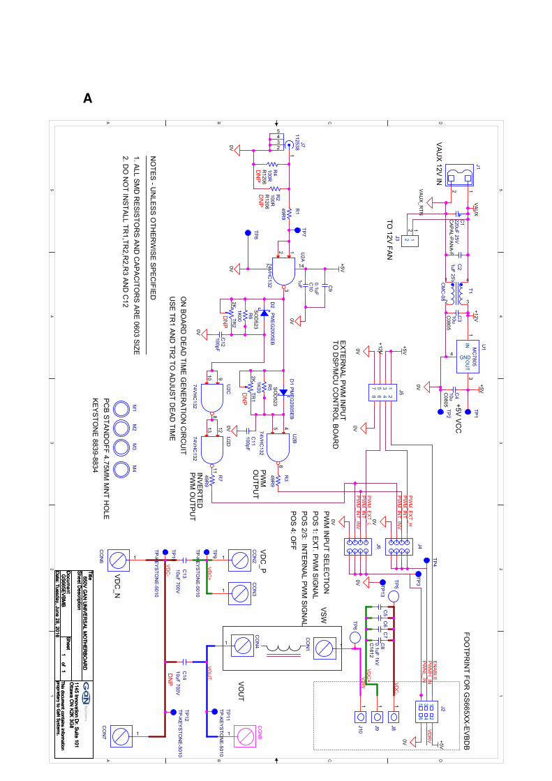
The introduction already mentioned that an existing GaN half bridge module, the GS66504Bwith the GS665EVBMB motherboard from GaN systems, will be used. This chapter willbriefly discuss the schematics, components and some specifications of the mother-board and the module provided. Furthermore reasoning of using an external PWMsignal using an FPGA will be discussed. At last the kind of measurements that will bedone are explained together with some reasoning
3.1 Motherboard (GS665EVBMB)
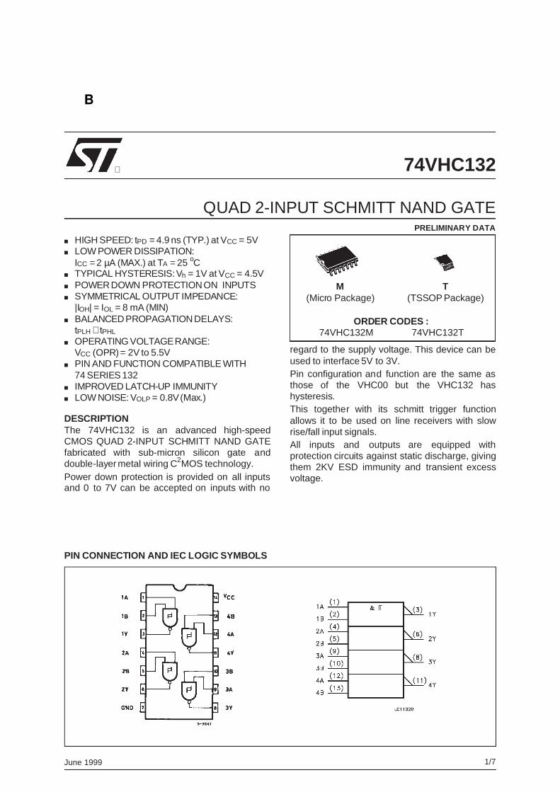
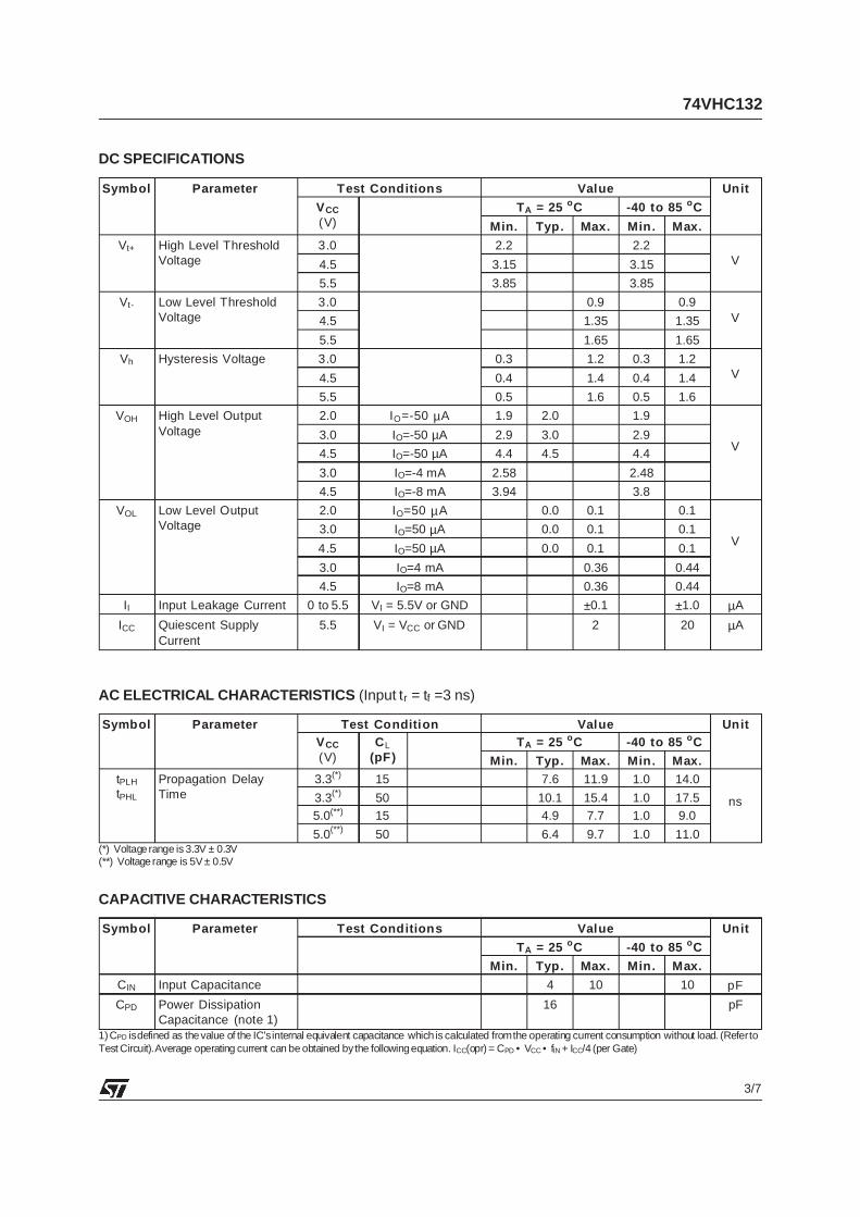
The design of the motherboard consists of an MC7805 and a 74VHC132. The MC7805is a DC-DC converter that generates 5 V from the 12 V input. The 5 V is used to powerthe components on the motherboard and on the module. The 74VHC132 is a schmitttrigger which uses a sine wave input to generate a PWM signal of the same frequency.The PWM signal consists of a high signal and a low signal with a deadtime of 100ns between the switches of the two. Deadtime is introduced to make sure the outputtransistors are not on at the same time, which would result in a short. The schmitttrigger is able to generate PWM signal with a frequency up to several megahertz. Theschematic of the motherboard and the useful pages of the data sheet of the schmitttrigger can be found in Appendix A and Appendix B respectively.
3.2 GaN module (GS66504B)
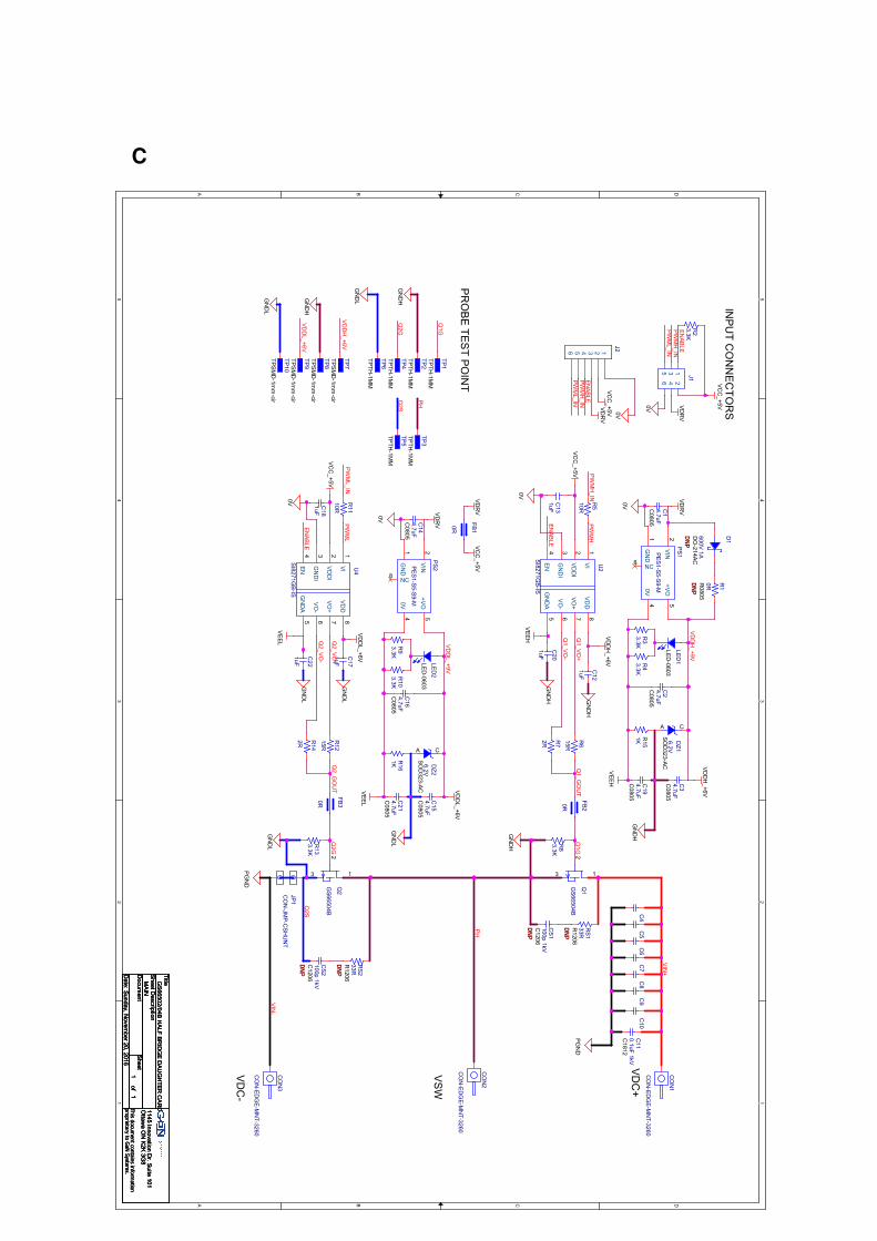
The Half Bridge module has, apart from the two GaN transistors, two gate drivers(SI8271GB-IS) and two 9 V DC-DC converters (PES1-S5-S9-M). Data sheets showthat the gate drivers have a typical rise and fall time of 10.5 ns and 13.3 ns respectivelyand uses the 9 V generated by the 9 V DC-DC converters to drive the gate. The inputPWM signals can be either 3.3 V or 5 V. The GaN transistors are specified to work upto drain source voltage of 650 V. Figures 3.1 and 3.2 show the design of one of the gatedrivers, including the output GaN transistor, and the 9 V DC-DC converter respectively.The entirety of the schematic can be found in appendix C, the relevant pages from thedata sheet of gate driver are shown in appendix D.
9
Figure 3.1: Circuit schematic of the gate driver
Figure 3.2: Circuit schematic of the 9V DC-DC converter
3.3 FPGA
Next to using the internal schmitt trigger for PWM generation an external PWM signalcan be applied directly to the gate drivers. This would be done using an FPGA. Theadvantage of using this FPGA is the possibility to easily and quickly modify input signalsfor example with regards to frequency, deadtime, rise and fall times. The FPGA iscapable of generating a PWM signal up to 1 MHz [10](to be published).
3.4 Method of Measuring
The FPGA can be used up to 1 MHz, measurements with the internal schmitt trigger willbe done up to 2 MHz because this will show that the module does not limit the signal upto 1 MHz and if the module works consistent even beyond 1 MHz. The system will betested with a input signal with a frequency of 10 kHz up to 2 MHz with both the internalPWM generated signal and a frequency of up to 1 MHz with the FPGA generated PWM
10

Output
Gate Q1
Gate Q2
Gate driver
Input
Schmitt trigger
PWM high
PWM low
Figure 3.3: Diagram of the module
Output
Gate Q1
Gate Q2
Gate driver
PWM high
PWM low
FPGA
Figure 3.4: Diagram of the module with the FPGA
signal. The Figures 3.3 and 3.4 show a diagram of the system without and with theFPGA respectively. The duty cycle will be 50%. Noting that the 100ns internal deadtime is not included in the duty cycle, so practically it is lower than 50% depending oninput frequency, on and off time have the same length. The duty cycle is not shownin the diagrams but the effect will be shown in the results section. For the FPGA afew measurements with several different dead times with a range of frequencies is alsodone to see what the influence of variable dead time is.The first measurement point of interest is the output of the schmitt trigger. Second pointis the output of both the gate drivers and the last point the output of the half bridge, theoutput will be measured loaded and unloaded with a linear impedance. For the FPGAmeasurements the same three points will be looked into, where the first point is not theoutput of the schmitt trigger but the output of the FPGA.
11
4 Measurements
This section will give a brief overview of measurements done and results. SeveralFigures will be shown in the appendix to not overcrowd this section with Figures.
4.1 Measurements with internal PWM
Measuring the system as explained in the previous sections resulted in the following.The PWM signal from the schmitt trigger, the gate signals and the output are measured.Figure 4.1 shows the PWM signal and the gate signal of the upper part of the half bridgeand the output, as shown in Figure 3.3. It shows measurements with an output voltageof 15 volt without a load and with several frequencies from 10 kHz up to 2 MHz. Theschmitt trigger has a rise a time of 2.7 ns. The falling flank of the gate transistor Q1has a step, this step is due to the dead time, the gate driver of Q1 has the output as areference voltage, so if the the gate driver turns off and transistor Q2 is not yet turnedon, the gate will drop with 9 V and will become the same as the output. Figure 4.2shows the same measurements as the previous Figure, but this time it shows the lowerpart of the module. From the Figures one can clearly see that rise time is not influencedby change in frequency. The rise time of the output signals is 3.4 ns, the fall times are3.6 ns.The following Figures, Figure 4.3 and 4.4, show an output voltage of 15, 30 and 45 voltand a frequency of 100 kHz. The overshoot, in case of Figure 4.3 is 30%, 27% and25% respectively and a rise time of around 3.9 ns for the 15 V output and around 9 nsfor the 30 V and 45 V output. The undershoot in case of Figure 4.4 25%, 21% and 17%respectively with a fall time of around 10 ns. The ringing is visibly different in the threecases. The ringing frequencies are crudely estimated by measuring the time betweenperiods of the visible signals, an FFT in matlab could not give an accurate insight in thespectrum due to lack of data points. The estimated frequencies are around 24 MHz,108 MHz, 250 MHz and 500 MHz, where for the higher output voltage the lower ringingfrequencies get more predominant than the high frequencies.
4.2 Measurements with FPGA generated PWM input signals
Now that several different points on the module have been measured the FPGA canadded as input signal. Figures 4.54.6 show the same signals as the section before, thistime the PWM signal is generated by the FPGA which is the top plot in the Figures. Thefrequencies shown are 100 kHz up to 600 kHz with an output amplitude of 15 V. The
12
-1 0 1 2 3 4 5
Time [s] 10-7
-5
0
5
10
15
20
Out
put [
V]
10 kHz20 kHz......1 MHz1.5 MHz2 MHz
-1 0 1 2 3 4 5
Time [s] 10-7
-10
0
10
20
30
Gat
e Q
1 [V
]
10 kHz20 kHz......1 MHz1.5 MHz2 MHz
-1 0 1 2 3 4 5
Time [s] 10-7
-2
0
2
4
6
PW
M S
igna
l [V
]
10 kHz20 kHz......1 MHz1.5 MHz2 MHz
[H]
Figure 4.1: From top to bottom: PWM signal schmitt trigger, gate signal Q1 and theoutput
13
-2 -1 0 1 2 3 4 5
Time [s] 10-7
-5
0
5
10
15
20
Out
put [
V]
10 kHz20 kHz......1 MHz1.5 MHz2 MHz
-2 -1 0 1 2 3 4 5
Time [s] 10-7
-10
-5
0
5
10
Gat
e si
gnal
Q2
[V]
10 kHz20 kHz......1 MHz1.5 MHz2 MHz
-2 -1 0 1 2 3 4 5
Time [s] 10-7
-2
0
2
4
6
PW
M s
igna
l [V
]
10 kHz20 kHz......1 MHz1.5 MHz2 MHz
[H]
Figure 4.2: From top to bottom: PWM signal schmitt trigger, gate signal Q2 and theoutput
14
-1 0 1 2 3 4 5
Time [s] 10-7
-0.2
0
0.2
0.4
0.6
0.8
1
1.2
1.4
Nor
mal
ized
out
put
15 V output30 V output45 V output
Figure 4.3: Normalized outputs of the rising flank with 15 V, 30 V and 45 V
15
-1 0 1 2 3 4 5
Time [s] 10-7
-0.4
-0.2
0
0.2
0.4
0.6
0.8
1
1.2
Nor
mal
ized
out
put
15 V output30 V output45 V output
Figure 4.4: Normalized outputs of the falling flank with 15 V, 30 V and 45 V
16

rise time and fall time of the output is comparable to the previous measured rise and falltimes with a rise time of around 3.4 ns and a fall time of around 3.6 ns. The rise time ofthe PWM signal generated by the FPGA is 12 ns.
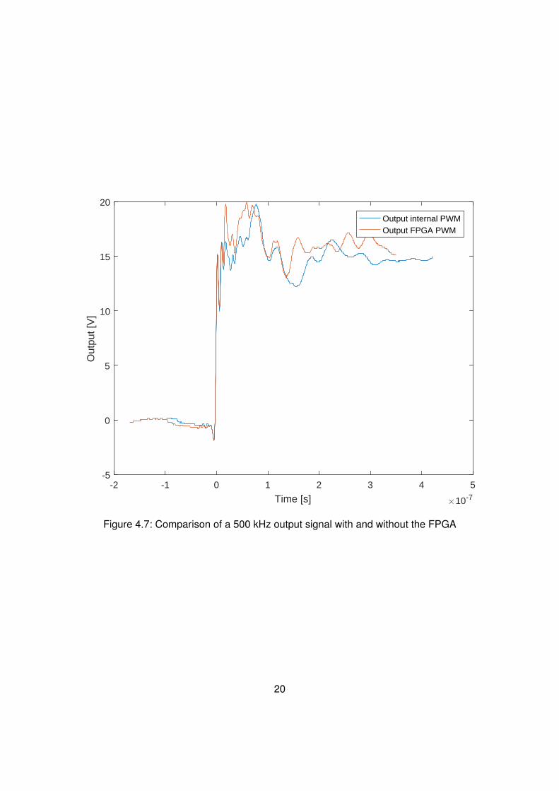
4.3 Comparison between the outputs with and without FPGA
For better comparison of the output signal, a signal of the output with and without theFPGA at 500 kHz is shown in Figure 4.7. The output amplitude is 15V, the overshoot isaround 32% for both signals
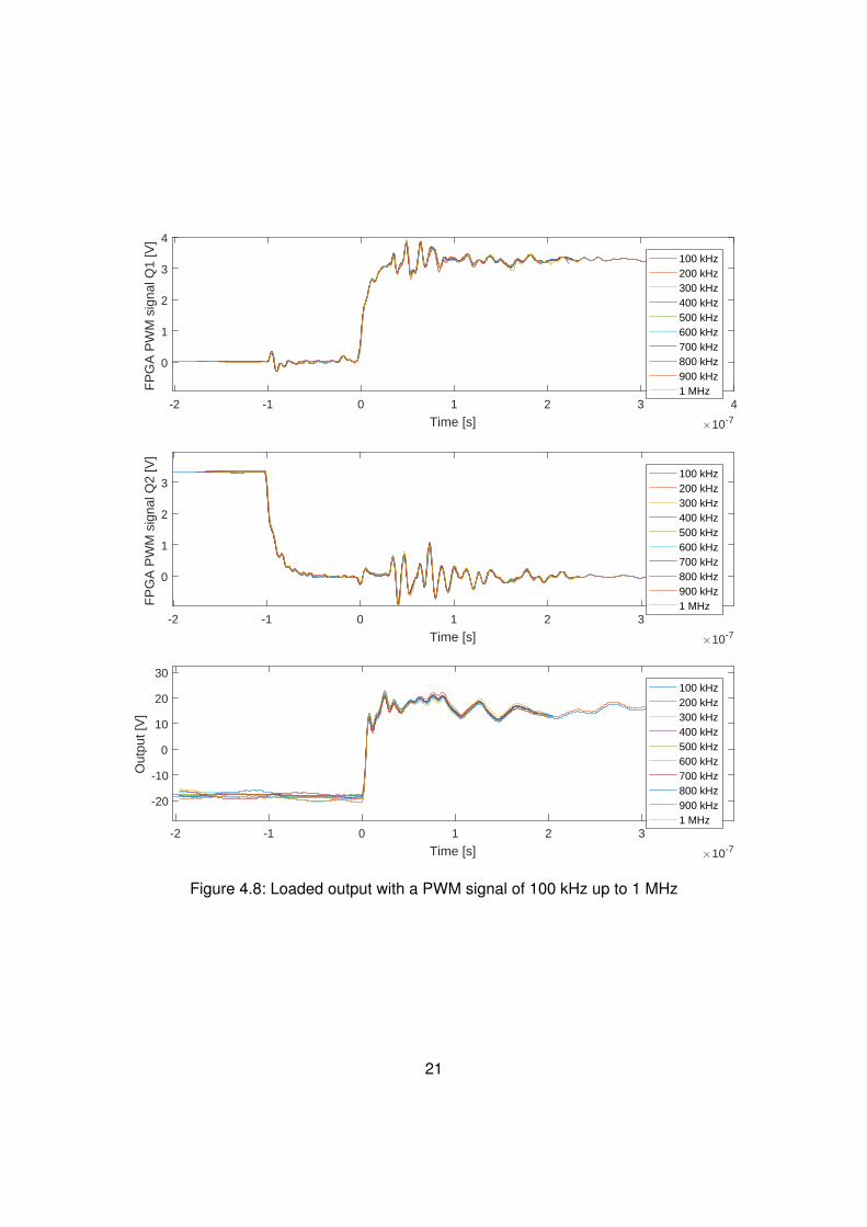
4.4 Measurements with load
All the previous Figures show signals with an unloaded output. The next few Figureswill show the output with a resistive load of 60Ω. Figures 4.8 and 4.9 show the twoinput signals generated by the FPGA and the output. Figure 8 shows the rising flank ofthe output where Figure 4.9 shows the falling flank of the output. The output amplitudeis 35 V, the frequencies used are 100 kHz up to 1 MHz and the dead time is 100 ns.The rise time is around 17 ns for every frequency, the fall time is around 4 ns for everyfrequency. The overshoot is 32% and the undershoot is 45% for all frequencies.
17

-4 -2 0 2 4 6 8 10
Time [s] 10-7
-5
0
5
10
15
20
25
Out
put [
V]
100 kHz200 kHz300 kHz400 kHz500 kHz600 kHz
-4 -2 0 2 4 6 8 10
Time [s] 10-7
-10
0
10
20
30
Gat
e Q
1 [V
]
100 kHz200 kHz300 kHz400 kHz500 kHz600 kHz
-4 -2 0 2 4 6 8 10
Time [s] 10-7
-1
0
1
2
3
4
PW
M S
igna
l FP
GA
[V] 100 kHz
200 kHz300 kHz400 kHz500 kHz600 kHz
Figure 4.5: Top to bottom: FPGA signal, gate signal Q1 and the output
18
-4 -2 0 2 4 6 8 10
Time [s] 10-7
-5
0
5
10
15
20
25
Out
put [
V]
100 kHz200 kHz300 kHz400 kHz500 kHz600 kHz
-4 -2 0 2 4 6 8 10
Time [s] 10-7
-10
-5
0
5
10
Gat
e Q
2 [V
]
100 kHz200 kHz300 kHz400 kHz500 kHz600 kHz
-4 -2 0 2 4 6 8 10
Time [s] 10-7
-2
0
2
4
6
PW
M S
igna
l FP
GA
[V] 100 kHz
200 kHz300 kHz400 kHz500 kHz600 kHz
Figure 4.6: Top to bottom: FPGA signal, gate signal Q2 and the output
19
-2 -1 0 1 2 3 4 5
Time [s] 10-7
-5
0
5
10
15
20
Out
put [
V]
Output internal PWMOutput FPGA PWM
Figure 4.7: Comparison of a 500 kHz output signal with and without the FPGA
20
-2 -1 0 1 2 3
Time [s] 10-7
-20
-10
0
10
20
30
Out
put [
V]
100 kHz200 kHz300 kHz400 kHz500 kHz600 kHz700 kHz800 kHz900 kHz1 MHz
-2 -1 0 1 2 3
Time [s] 10-7
0
1
2
3
FP
GA
PW
M s
igna
l Q2
[V]
100 kHz200 kHz300 kHz400 kHz500 kHz600 kHz700 kHz800 kHz900 kHz1 MHz
-2 -1 0 1 2 3 4
Time [s] 10-7
0
1
2
3
4
FP
GA
PW
M s
igna
l Q1
[V]
100 kHz200 kHz300 kHz400 kHz500 kHz600 kHz700 kHz800 kHz900 kHz1 MHz
Figure 4.8: Loaded output with a PWM signal of 100 kHz up to 1 MHz
21

-5 -4 -3 -2 -1 0 1 2 3 4 5
Time [s] 10-7
-30
-20
-10
0
10
20
Out
put [
V]
100 kHz200 kHz300 kHz400 kHz500 kHz600 kHz700 kHz800 kHz900 kHz1 MHz
-5 -4 -3 -2 -1 0 1 2 3 4 5
Time [s] 10-7
-1
0
1
2
3
4
FP
GA
PW
M s
igna
l Q2
[V]
100 kHz200 kHz300 kHz400 kHz500 kHz600 kHz700 kHz800 kHz900 kHz1 MHz
-5 -4 -3 -2 -1 0 1 2 3 4 5
Time [s] 10-7
-1
0
1
2
3
4
FP
GA
PW
M s
igna
l Q1
[V]
100 kHz200 kHz300 kHz400 kHz500 kHz600 kHz700 kHz800 kHz900 kHz1 MHz
Figure 4.9: Loaded output with a PWM signal of 100 kHz up to 1 MHz
22
60 80 100 120 140 160 180 200
Deadtime [ns]
0
5
10
15
20
25
30
35
40O
vers
hoot
[per
cent
age]
100 kHz500 kHz750 kHz1 MHz
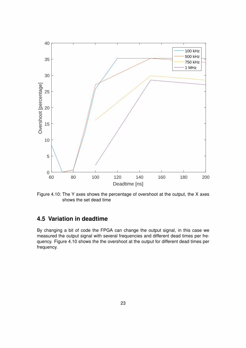
Figure 4.10: The Y axes shows the percentage of overshoot at the output, the X axesshows the set dead time
4.5 Variation in deadtime
By changing a bit of code the FPGA can change the output signal, in this case wemeasured the output signal with several frequencies and different dead times per fre-quency. Figure 4.10 shows the the overshoot at the output for different dead times perfrequency.
23
5 Evaluation Discussion
5.1 Conclusion
The previous section of this report showed several measurements. Figures 4.1 and 4.2show the ringing generated at the output is independent of the frequency where theinput frequency is increased up to a frequency of 2 MHz. Also can be concluded thatthe rise and fall time stay the same for an unloaded Half-Bridge. Where the rise and falltime is the amount of time needed for the signal to get to its end state.Figures 4.3 and 4.4 compares the same frequency with different output voltages. Therise times seem to get higher for higher voltage outputs, this is probably due to theringing frequency interfering and keeping the signal under the 90% signal mark, sincerise and fall time is the time it takes for the signal to get from 10% to 90%. Overshootis comparable percent wise, from that can be concluded that the amount of overshootscales linearly with output voltage. The data shows ringing frequencies from 12 MHz upto 250 MHz, where it seems for higher output voltages the lower ringing frequencies getmore predominant. The signals have similar rise time which means the 45 V signal hasa higher dV
dt than the 15 V and 30 V signals, this will have an influence on the parasiticsand thus the ringing.Figure 4.7 shows the effect of the FPGA on the output signal with the same outputamplitude and same input frequency. The rise time is not affected by the FPGA, alsothe ringing frequencies range from 24 MHz to 500 MHz.In the case of a loaded output the ringing frequencies are slightly different to the un-loaded case, they are in the range of 20 MHz to around 200 MHz shown in Figures 4.8and 4.9. These Figures also show that the FPGA is capable of driving the Half-Bridgemodule up to a frequency of 1 MHz, furthermore it shows that a load does not influ-ence characteristics of the signal if the output voltage is constant and the frequency ischanged. The last Figure shows that there is a relation between overshoot and deadtime, dead time can be used to decrease overshoot and influence EMI.
5.2 Future research
The report has shown that the module is capable of switching high frequencies up to 2MHz and that the FPGA can drive the module as intended up to 1 MHz. Shown is thatdead time has an influence on overshoot, a programmable FPGA might show usefulin case the module will be stacked in a M3C system, where a slight variation in signalvariables might make the difference between being electromagnetic compatibility or not.
24

Future research should look into the relation between dead time and the overshoot andringing of the signal, also include several different output voltages and loads to see ifresults from this paper also apply to higher voltages up to 600 Volt.
25

Appendix
The following pages show relevant documents. It consists of parts of data sheets andcircuit diagrams.
55
44
33
22
11
DD
CC
BB
AA
VAUX 12V IN
EXTERN
AL PWM
INPU
TTO
DSP/M
CU
CO
NTR
OL BO
ARD
PWM
INPU
T SELECTIO
N
ON
BOAR
D D
EAD TIM
E GEN
ERATIO
N C
IRC
UIT
USE TR
1 AND
TR2 TO
ADJU
ST DEAD
TIME
POS 2/3: IN
TERN
AL PWM
SIGN
AL
+5V VCC
POS 1: EXT. PW
M SIG
NAL
PWM
O
UTPU
T
INVER
TED
PWM
OU
TPUT
VDC
_P
VDC
_N
VOU
T
VSW
DN
PD
NP
TO 12V FAN
DN
P
DN
P
DN
P
NO
TES - UN
LESS OTH
ERW
ISE SPECIFIED
1. ALL SMD
RESISTO
RS AN
D C
APACITO
RS AR
E 0603 SIZE
POS 4: O
FF
2. DO
NO
T INSTALL TR
1,TR2,R
2,R3 AN
D C
12
FOO
TPRIN
T FOR
GS665XX-EVBD
B
PCB STAN
DO
FF 4.75MM
MN
T HO
LEKEYSTO
NE 8839-8834
+5VVAU
X
0V0V
+5V
0V
0V
0V
0V0V
0V
0V0V
+5V
+12V
VAUX_R
TN
+12V
+5V
0V
0V
Title
Docum
ent
Date:
Sheetof
This document contains inform
ationproprietary to GaN System
s.
Sheet Description
1145 Innovation Dr. Suite 101
Ottaw
a ON
K2K 3G8
650V GAN
UN
IVERSAL M
OTH
ERBO
ARD
11
Tuesday, June 28, 2016G
S665EVBMB
Title
Docum
ent
Date:
Sheetof
This document contains inform
ationproprietary to GaN System
s.
Sheet Description
1145 Innovation Dr. Suite 101
Ottaw
a ON
K2K 3G8
650V GAN
UN
IVERSAL M
OTH
ERBO
ARD
11
Tuesday, June 28, 2016G
S665EVBMB
Title
Docum
ent
Date:
Sheetof
This document contains inform
ationproprietary to GaN System
s.
Sheet Description
1145 Innovation Dr. Suite 101
Ottaw
a ON
K2K 3G8
650V GAN
UN
IVERSAL M
OTH
ERBO
ARD
11
Tuesday, June 28, 2016G
S665EVBMB
CO
N7 1
R3
49R9
C4
10uC
0805
CO
N41
TP5
J2
12
34
56
J112
TP4
CO
N21
C1
220uF 25VC
APAL-PANA-F
TP13J9
1
D1
PMEG
2005EB
SOD
523
C12
100pF
C14
10uF 700V
J4
TP12TP-KEYSTO
NE-5010
R7
49R9
C10
1uF
CO
N51
J81
C9
0.1uF
R6
1K00
TP2
TP7
J6
TR1
2K
TP11TP-KEYSTO
NE-5010
C8
0.1uF 1kVC
1812
TP9
TP-KEYSTON
E-5010
R1
49R9
U2B
74VHC
132
456
TP6
CO
N31
C3
10uC
0805
T1
CM
C-08
1 4
2 3
C2
1uF 25V
U2C
74VHC
132
9108
J5
12
34
5768
M1
M2
J3 11
22
C7
C11
100pF
D2
PMEG
2005EB
SOD
523TP8
U2D
74VHC
132
121311
R4
100RR
1206
CO
N6 1
C5
M3
M4
U1M
C7805
IN1
OU
T3
GND4
J7112538
1
2345
TP3
R2
100RR
1206
C13
10uF 700VTP10
TP-KEYSTON
E-5010
C6
U2A
74VHC
132
312
147
TP1
CO
N1 1
R5
1K00
TR2
2K
J101
PWM
_EXT_HPW
M_IN
TPW
M_IN
T_INV
PWM
_EXT_LPW
M_IN
TPW
M_IN
T_INV
ENABLE
VDC
-
VDC
+
VDC
-
VOU
T VSW
PWM
H_IN
PWN
L_IN
VDC
+
VDR
V
A
74VHC132
QUAD 2-INPUT SCHMITT NAND GATEPRELIMINARY DATA
June 1999
HIGH SPEED: tPD = 4.9 ns (TYP.) at VCC = 5V LOW POWER DISSIPATION:
ICC =2 µA (MAX.) at TA = 25 oC TYPICAL HYSTERESIS:Vh = 1V at VCC = 4.5V POWERDOWN PROTECTIONON INPUTS SYMMETRICAL OUTPUT IMPEDANCE:
|IOH| = IOL = 8 mA (MIN) BALANCEDPROPAGATIONDELAYS:
tPLH ≅ tPHL
OPERATING VOLTAGERANGE:VCC (OPR)= 2V to 5.5V
PIN AND FUNCTION COMPATIBLE WITH74 SERIES 132
IMPROVED LATCH-UP IMMUNITY LOW NOISE: VOLP = 0.8V(Max.)
DESCRIPTIONThe 74VHC132 is an advanced high-speedCMOS QUAD 2-INPUT SCHMITT NAND GATEfabricated with sub-micron silicon gate anddouble-layer metal wiring C2MOS technology.Power down protection is provided on all inputsand 0 to 7V can be accepted on inputs with no
regard to the supply voltage. This device can beused to interface 5V to 3V.Pin configuration and function are the same asthose of the VHC00 but the VHC132 hashysteresis.This together with its schmitt trigger functionallows it to be used on line receivers with slowrise/fall input signals.All inputs and outputs are equipped withprotection circuits against static discharge, givingthem 2KV ESD immunity and transient excessvoltage.
PIN CONNECTION AND IEC LOGIC SYMBOLS
ORDER CODES :74VHC132M 74VHC132T
M(Micro Package)
T(TSSOP Package)
1/7
B

INPUT EQUIVALENT CIRCUIT
ABSOLUTE MAXIMUM RATINGS
Symbol Parameter Value Unit
VCC Supply Voltage -0.5 to +7.0 V
VI DC Input Voltage -0.5 to +7.0 V
VO DC Output Voltage -0.5 to VCC + 0.5 V
IIK DC Input Diode Current - 20 mA
IOK DC Output Diode Current ± 20 mA
IO DC Output Current ± 25 mA
ICC or IGND DC VCC or Ground Current ± 50 mA
Tstg Storage Temperature -65 to +150 oC
TL Lead Temperature (10 sec) 300 oCAbsoluteMaximum Ratingsarethose values beyond whichdamage to the device may occur. Functional operation under these condition isnot implied.
TRUTH TABLE
A B Y
L L H
L H H
H L H
H H L
PIN DESCRIPTION
PIN No SYMBOL NAME AND FUNCTION
1, 4, 9, 12 1A to 4A Data Inputs
2, 5, 10, 13 1B to 4B Data Inputs
3, 6, 8, 11 1Y to 4Y Data Outputs
7 GND Ground (0V)
14 VCC Positive Supply Voltage
RECOMMENDED OPERATING CONDITIONS
Symbol Parameter Value Unit
VCC Supply Voltage 2.0 to 5.5 V
VI Input Voltage 0 to 5.5 V
VO Output Voltage 0 to VCC V
Top Operating Temperature -40 to +85 oC
74VHC132
2/7
CAPACITIVE CHARACTERISTICS
Symbol Parameter Test Conditions Value Unit
TA = 25 oC -40 to 85 oC
Min. Typ. Max. Min. Max.
CIN Input Capacitance 4 10 10 pF
CPD Power DissipationCapacitance (note 1)
16 pF
1)CPD isdefined as thevalue of the IC’sinternal equivalent capacitance which is calculated fromthe operating current consumption without load. (RefertoTest Circuit).Average operating current can be obtained bythe followingequation. ICC(opr) = CPD • VCC • fIN + ICC/4 (per Gate)
AC ELECTRICAL CHARACTERISTICS (Input tr = tf =3 ns)
Symbol Parameter Test Condition Value UnitVCC
(V)CL
(pF)TA = 25 oC -40 to 85 oC
Min. Typ. Max. Min. Max.tPLH
tPHL
Propagation DelayTime
3.3(*) 15 7.6 11.9 1.0 14.0
ns3.3(*) 50 10.1 15.4 1.0 17.55.0(**) 15 4.9 7.7 1.0 9.0
5.0(**) 50 6.4 9.7 1.0 11.0(*) Voltagerange is 3.3V ± 0.3V(**) Voltagerange is 5V ± 0.5V
DC SPECIFICATIONS
Symbol Parameter Test Conditions Value Unit
VCC
(V)TA = 25 oC -40 to 85 oC
Min. Typ. Max. Min. Max.
Vt+ High Level ThresholdVoltage
3.0 2.2 2.2V4.5 3.15 3.15
5.5 3.85 3.85
Vt- Low Level ThresholdVoltage
3.0 0.9 0.9V4.5 1.35 1.35
5.5 1.65 1.65
Vh Hysteresis Voltage 3.0 0.3 1.2 0.3 1.2V4.5 0.4 1.4 0.4 1.4
5.5 0.5 1.6 0.5 1.6
VOH High Level OutputVoltage
2.0 IO=-50 µA 1.9 2.0 1.9
V3.0 IO=-50 µA 2.9 3.0 2.9
4.5 IO=-50 µA 4.4 4.5 4.4
3.0 IO=-4 mA 2.58 2.48
4.5 IO=-8 mA 3.94 3.8
VOL Low Level OutputVoltage
2.0 IO=50 µA 0.0 0.1 0.1
V3.0 IO=50 µA 0.0 0.1 0.1
4.5 IO=50 µA 0.0 0.1 0.1
3.0 IO=4 mA 0.36 0.44
4.5 IO=8 mA 0.36 0.44
II Input Leakage Current 0 to 5.5 VI = 5.5V or GND ±0.1 ±1.0 µA
ICC Quiescent SupplyCurrent
5.5 VI = VCC or GND 2 20 µA
74VHC132
3/7
55
44
33
22
11
DD
CC
BB
AA
VD
C+
VS
W
VD
C-
PR
OB
E T
ES
T P
OIN
T
INP
UT
CO
NN
EC
TO
RS
DNPDNP
DNP
DNP
DNP
DNP
0V
VD
RV
VD
DH
_+6V
PG
ND
PG
ND
GN
DH
VD
RV
VC
C_+
5V
GN
DH
VD
DH
_+6V
VC
C_+
5V
0V
GN
DL
VD
DL_+
6V
0V
VC
C_+
5V
0V
VD
RV
GN
DH
GN
DLGN
DL
GN
DH
VC
C_+
5VV
DR
V
0V
VC
C_+
5VVD
RV
0V
VE
EH
GN
DH
GN
DH
VD
DL_+
6V
GN
DL
VE
EL
VE
EL
GN
DL
GN
DL
VE
EH
Title
Docum
ent
Date:
Sheet
ofThis docum
ent contains information
proprietary to GaN
Systems.
Sheet D
escription1145 Innovation D
r. Suite 101
Ottaw
a ON
K2K
3G8
GS
66502/04B H
ALF
BR
IDG
E D
AU
GH
TE
R C
AR
D
11
Sunday, N
ovember 20, 2016
MA
IN
Title
Docum
ent
Date:
Sheet
ofThis docum
ent contains information
proprietary to GaN
Systems.
Sheet D
escription1145 Innovation D
r. Suite 101
Ottaw
a ON
K2K
3G8
GS
66502/04B H
ALF
BR
IDG
E D
AU
GH
TE
R C
AR
D
11
Sunday, N
ovember 20, 2016
MA
IN
Title
Docum
ent
Date:
Sheet
ofThis docum
ent contains information
proprietary to GaN
Systems.
Sheet D
escription1145 Innovation D
r. Suite 101
Ottaw
a ON
K2K
3G8
GS
66502/04B H
ALF
BR
IDG
E D
AU
GH
TE
R C
AR
D
11
Sunday, N
ovember 20, 2016
MA
IN
PS
1PE
S1-S
5-S9-M
GN
D1
VIN
2+
VO
5
0V
4
NC8
RS
133RR
1206
CO
N3
CO
N-E
DG
E-M
NT
-3260
J1
12
34
56
C11
0.1uF 1kV
C1812
TP
9
TP
SM
D-1m
m-cir
J2123456
R4
3.3K
TP
6
TP
TH
-1MM
R11
10R
U2
SI8271G
B-IS
VI
1
VD
DI
2
GN
DI
3
EN
4G
ND
A5
VO
-6
VO
+7
VD
D8
C22
1uF
R13
3.3K
R15
1K
FB
2
0R
C3
4.7uFC
0805
JP1
CO
N-JM
P-C
SH
UN
T
CS
1100p 1kVC
1206
C16
4.7uFC
0805
C18
1uF
C21
4.7uFC
0805
C5
TP
2
TP
TH
-1MM
C15
4.7uFC
0805
R6
15R
C20
1uF
R10
3.3K
R2
3.3K
TP
10
TP
SM
D-1m
m-cir
CO
N1
CO
N-E
DG
E-M
NT
-3260
FB
1
0R
FB
3
0R
C14
4.7uFC
0805
TP
3
TP
TH
-1MM
C12
1uF
R3
3.3K
R1
0RR0805
U4
SI8271G
B-IS
VI
1
VD
DI
2
GN
DI
3
EN
4G
ND
A5
VO
-6
VO
+7
VD
D8
C6
C2
4.7uFC
0805
R12
15R
C8
C17
1uF
DZ
26.2V
SO
D323-A
C
A C
R7
2R
Q1
GS
66504B
1
2
3
TP
8
TP
SM
D-1m
m-cir
TP
4
TP
TH
-1MM
C9
R9
3.3K
R5
10R
TP
1
TP
TH
-1MM
PS
2PE
S1-S
5-S9-M
GN
D1
VIN
2+
VO
5
0V
4
NC8
CO
N2
CO
N-E
DG
E-M
NT
-3260
C4
RS
233RR
1206
R8
3.3K
D1
600V 1A
DO
-214AC
TP
5
TP
TH
-1MM
R14
2R
TP
7
TP
SM
D-1m
m-cir
LED
1
LED
-0603
C10
R16
1K
C19
4.7uFC
0805
LED
2
LED
-0603
Q2
GS
66504B
1
2
3
C7
DZ
16.2V
SO
D323-A
C
A C
C1
4.7uFC
0805
CS
2100p 1kVC
1206
C13
1uF
VIN
+
PH
Q1G
VIN
-
Q2S
Q1_G
OU
TQ
1_VO
+
Q1_V
O-
VD
DH
_+9V
Q2G
Q2_G
OU
TQ
2_VO
+
Q2_V
O-
VD
DL_+
9V
PW
MH
_IN
PW
ML_IN
Q1G
Q2G
PH
Q2S
VD
DH
_+6V
VD
DL_+
6V
PW
MH
PW
ML
EN
AB
LE
EN
AB
LEP
WM
H_IN
PW
ML_IN
EN
AB
LE
EN
AB
LEP
WM
H_IN
PW
ML_IN
C
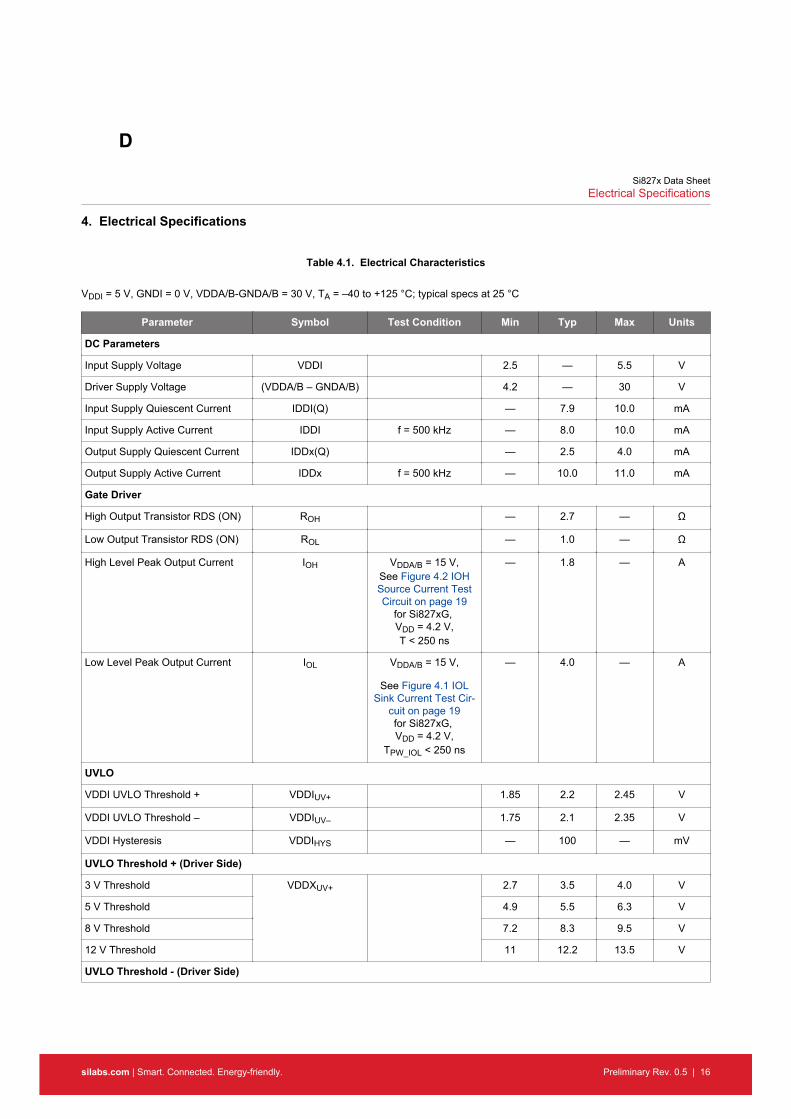
4. Electrical Specifications
Table 4.1. Electrical Characteristics
VDDI = 5 V, GNDI = 0 V, VDDA/B-GNDA/B = 30 V, TA = –40 to +125 °C; typical specs at 25 °C
Parameter Symbol Test Condition Min Typ Max Units
DC Parameters
Input Supply Voltage VDDI 2.5 — 5.5 V
Driver Supply Voltage (VDDA/B – GNDA/B) 4.2 — 30 V
Input Supply Quiescent Current IDDI(Q) — 7.9 10.0 mA
Input Supply Active Current IDDI f = 500 kHz — 8.0 10.0 mA
Output Supply Quiescent Current IDDx(Q) — 2.5 4.0 mA
Output Supply Active Current IDDx f = 500 kHz — 10.0 11.0 mA
Gate Driver
High Output Transistor RDS (ON) ROH — 2.7 — Ω
Low Output Transistor RDS (ΟΝ) ROL — 1.0 — Ω
High Level Peak Output Current IOH VDDA/B = 15 V,See Figure 4.2 IOHSource Current TestCircuit on page 19
for Si827xG, VDD = 4.2 V,T < 250 ns
— 1.8 — A
Low Level Peak Output Current IOL VDDA/B = 15 V,
See Figure 4.1 IOLSink Current Test Cir-
cuit on page 19for Si827xG, VDD = 4.2 V,
TPW_IOL < 250 ns
— 4.0 — A
UVLO
VDDI UVLO Threshold + VDDIUV+ 1.85 2.2 2.45 V
VDDI UVLO Threshold – VDDIUV– 1.75 2.1 2.35 V
VDDI Hysteresis VDDIHYS — 100 — mV
UVLO Threshold + (Driver Side)
3 V Threshold VDDXUV+ 2.7 3.5 4.0 V
5 V Threshold 4.9 5.5 6.3 V
8 V Threshold 7.2 8.3 9.5 V
12 V Threshold 11 12.2 13.5 V
UVLO Threshold - (Driver Side)
Si827x Data SheetElectrical Specifications
silabs.com | Smart. Connected. Energy-friendly. Preliminary Rev. 0.5 | 16
D
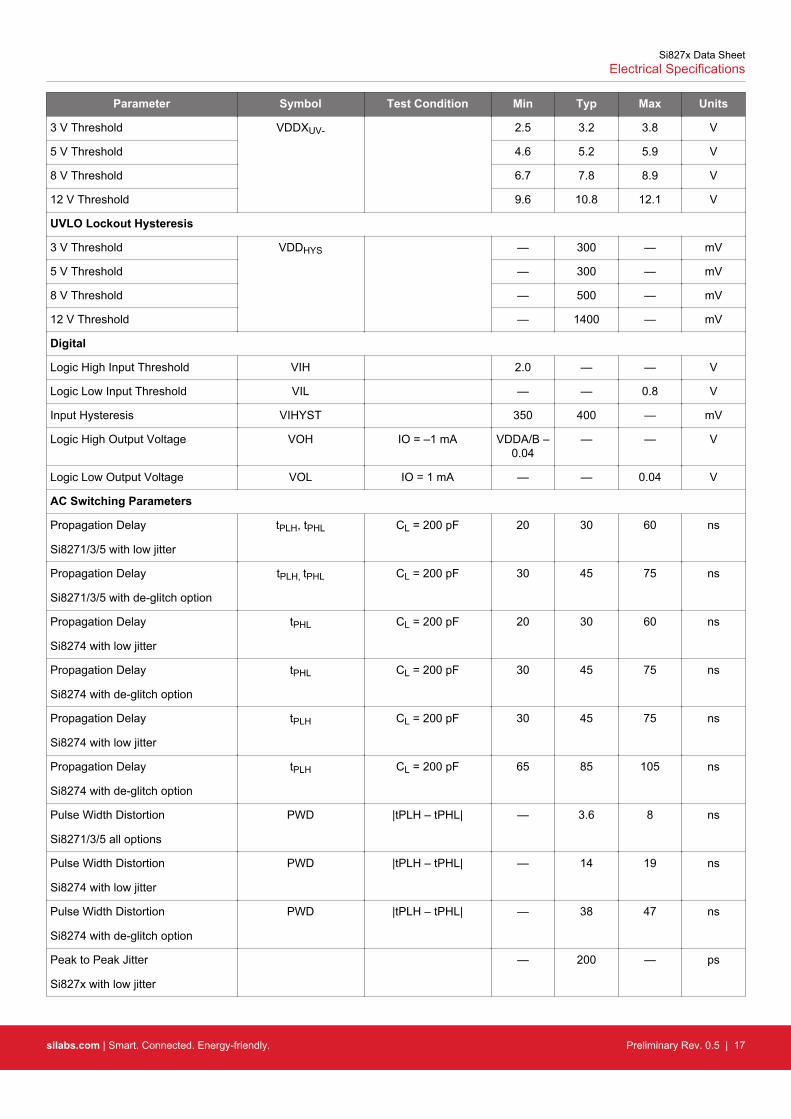
Parameter Symbol Test Condition Min Typ Max Units
3 V Threshold VDDXUV- 2.5 3.2 3.8 V
5 V Threshold 4.6 5.2 5.9 V
8 V Threshold 6.7 7.8 8.9 V
12 V Threshold 9.6 10.8 12.1 V
UVLO Lockout Hysteresis
3 V Threshold VDDHYS — 300 — mV
5 V Threshold — 300 — mV
8 V Threshold — 500 — mV
12 V Threshold — 1400 — mV
Digital
Logic High Input Threshold VIH 2.0 — — V
Logic Low Input Threshold VIL — — 0.8 V
Input Hysteresis VIHYST 350 400 — mV
Logic High Output Voltage VOH IO = –1 mA VDDA/B –0.04
— — V
Logic Low Output Voltage VOL IO = 1 mA — — 0.04 V
AC Switching Parameters
Propagation Delay
Si8271/3/5 with low jitter
tPLH, tPHL CL = 200 pF 20 30 60 ns
Propagation Delay
Si8271/3/5 with de-glitch option
tPLH, tPHL CL = 200 pF 30 45 75 ns
Propagation Delay
Si8274 with low jitter
tPHL CL = 200 pF 20 30 60 ns
Propagation Delay
Si8274 with de-glitch option
tPHL CL = 200 pF 30 45 75 ns
Propagation Delay
Si8274 with low jitter
tPLH CL = 200 pF 30 45 75 ns
Propagation Delay
Si8274 with de-glitch option
tPLH CL = 200 pF 65 85 105 ns
Pulse Width Distortion
Si8271/3/5 all options
PWD |tPLH – tPHL| — 3.6 8 ns
Pulse Width Distortion
Si8274 with low jitter
PWD |tPLH – tPHL| — 14 19 ns
Pulse Width Distortion
Si8274 with de-glitch option
PWD |tPLH – tPHL| — 38 47 ns
Peak to Peak Jitter
Si827x with low jitter
— 200 — ps
Si827x Data SheetElectrical Specifications
silabs.com | Smart. Connected. Energy-friendly. Preliminary Rev. 0.5 | 17
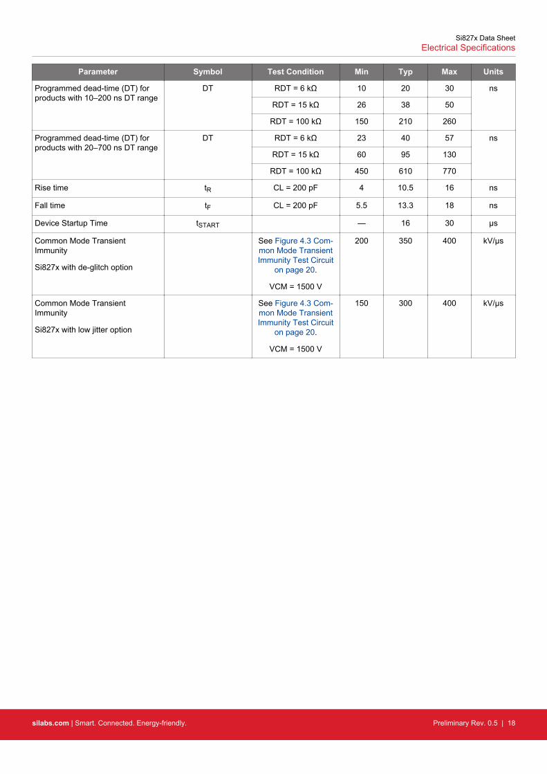
Parameter Symbol Test Condition Min Typ Max Units
Programmed dead-time (DT) forproducts with 10–200 ns DT range
DT RDT = 6 kΩ 10 20 30 ns
RDT = 15 kΩ 26 38 50
RDT = 100 kΩ 150 210 260
Programmed dead-time (DT) forproducts with 20–700 ns DT range
DT RDT = 6 kΩ 23 40 57 ns
RDT = 15 kΩ 60 95 130
RDT = 100 kΩ 450 610 770
Rise time tR CL = 200 pF 4 10.5 16 ns
Fall time tF CL = 200 pF 5.5 13.3 18 ns
Device Startup Time tSTART — 16 30 µs
Common Mode TransientImmunity
Si827x with de-glitch option
See Figure 4.3 Com-mon Mode TransientImmunity Test Circuit
on page 20.
VCM = 1500 V
200 350 400 kV/µs
Common Mode TransientImmunity
Si827x with low jitter option
See Figure 4.3 Com-mon Mode TransientImmunity Test Circuit
on page 20.
VCM = 1500 V
150 300 400 kV/µs
Si827x Data SheetElectrical Specifications
silabs.com | Smart. Connected. Energy-friendly. Preliminary Rev. 0.5 | 18
List of References
[1] G. Deboy, M. Treu, O. Haeberlen, and D. Neumayr, “Si, SiC and GaN power de-vices: An unbiased view on key performance indicators,” Tech. Dig. - Int. ElectronDevices Meet. IEDM, pp. 20.2.1–20.2.4, 2017.
[2] M. Gagic, T. Hailu, and J. A. Ferreira, “Multifunctional modular multilevel converter-based systems bottom-up approach to system design,” 2016 IEEE 8th Int. PowerElectron. Motion Control Conf. IPEMC-ECCE Asia 2016, pp. 944–951, 2016.
[3] N. M. Kirby, L. Xu, M. Luckett, and W. Siepmann, “HVDC transmission for largeoffshore wind farms,” Power Eng. J., vol. 16, no. 3, pp. 135–141, 2002.
[4] M. Starke, L. M. Tolbert, and B. Ozpineci, “AC vs. DC distribution: A loss compar-ison,” Transm. Distrib. Expo. Conf. 2008 IEEE PES Powering Towar. Futur. PIMS2008, 2008.
[5] D. Nilsson and A. Sannino, “Efficiency analysis of low-and medium-voltage DCdistribution systems,” Power Eng. Soc. Gen. . . . , pp. 1–7, 2004.
[6] J. A. Ferreira, “The multilevel modular DC converter,” IEEE Trans. Power Electron.,vol. 28, no. 10, pp. 4460–4465, 2013.
[7] ——, “Nestled secondary power loops in multilevel modular converters,” 2014IEEE 15th Work. Control Model. Power Electron. COMPEL 2014, pp. 1–9, 2014.
[8] K. Huang and J. A. Ferreira, “Two operational modes of the modular multilevel DCconverter,” 9th Int. Conf. Power Electron. - ECCE Asia ”Green World with PowerElectron. ICPE 2015-ECCE Asia, pp. 1347–1354, 2015.
[9] C. R. Paul, Introduction to Electromagnetic Compatibility, 1992, vol. 38, no. 7-8.
[10] N. Moonen, F. Buesink, and F. Leferink, “MATLAB Controllable FPGA-BasedsPWM Generator for High Switching Frequency Multi-Level Converters with Con-trollable Output Frequency.”