Embed Size (px)
Citation preview

GaAs based Vertical-Cavity Surface-
Emitting Transistor-Lasers
Yu Xiang
Doctoral Thesis in Microelectronics and Applied Physics
Stockholm, Sweden 2014
Integrated Devices and Circuits
School of Information and Communication Technology
KTH Royal Institute of Technology

A dissertation submitted to KTH Royal Institute of Technology, Stockholm, Sweden, in particular
fulfillment of the requirements for the degree of Technologie Doktor (Doctor of Philosophy). The public
defense will take place on 19 December 2014, 10:00 a.m. in Sal C, Electrum, Isafordsgatan 22, Kista
TRITA-ICT/MAP AVH Report 2014:16
ISSN 1653-7610
ISRN KTH/ICT-MAP/AVH-2014:16-SE
ISBN 978-91-7595-363-2
© Yu Xiang, 2014
Printed by US-AB, Stockholm, 2014

III
Abstract
The ever-increasing demand for broadband capacity of the global optical communication networks
puts enormous requirements on the semiconductor laser used in the optical transmitter. Industrial
standard bodies for optical communication project requirements of single-channel data rates as high
as 100 Gbit/s around year 2020. This is a significant step with respect to today's technology which is
only at the verge of introducing 25 Gbit/s emitters. The preferred light source for these applications is
the vertical-cavity surface-emitting laser (VCSEL) which can offer cost- and power-efficient directly
modulated operation. However, it has proven extremely difficult to push the modulation bandwidth of
VCSELs beyond 30 GHz and radically new device concepts are demanded to meet the upcoming needs.
One such new device paradigm consists of the transistor laser which is the fusion of a semiconductor
laser and a high-speed heterojunction bipolar transistor (HBT) into a single device, with potential
significant advantages in modulation bandwidth, noise properties and novel functionality by virtue of
the three-terminal configuration. The present thesis deals with the design, fabrication and analysis of
vertical-cavity surface-emitting transistor-lasers (T-VCSELs), a device previously not realized or
investigated in great detail.
GaAs-based T-VCSELs are investigated both theoretically and experimentally. A three-dimensional
model is set up with a commercial software package and used for performance predictions and analysis
as well as design and optimization purposes. It is concluded that a T-VCSEL biased in the common-
base configuration may have a bandwidth surpassing those of conventional diode-type VCSELs or a T-
VCSEL itself in the common-emitter configuration. Fabricated T-VCSELs make use of an epitaxial
regrowth design to homogeneously integrate an AlGaAs/GaAs HBT and an InGaAs/GaAs VCSEL. An
intracavity contacting scheme involving all three terminals, undoped distributed Bragg reflectors and
modulation doping are used to ensure a low-loss laser structure. The first generation of devices showed
sub-mA range base threshold current in combination with a high output power close to 2 mW but did
not fulfill the requirements for a fully operational transistor laser since the transistor went into
saturation before the onset of lasing (IBsat<IBth). From numerical simulations this premature saturation
was demonstrated being due to a lateral potential variation within the device and large voltage drops
along the base and collector regions. As a remedy to this problem the base region was redesigned for a
reduced resistance and transistor current gain, and the saturation current could thereby be extended
well beyond threshold. These devices showed excellent transistor-laser characteristics with clear gain-
compression at threshold, mA-range base threshold current, mW-range output power, high-
temperature operation to at least 60°C, low collector-emitter offset voltage and record-low power
dissipation during lasing. Furthermore, the collector-current breakdown characteristics was
investigated in some detail and it is concluded that this, in contrast to previous models, presumably
not is due to an intracavity photon reabsorption process but rather to a quantum-well band-filling
effect.

IV
List of appended papers
Paper A: Design and modeling of a transistor vertical-cavity surface-
emitting laser W. Shi, B. Faraji, M. Greenberg, L. Chrotowski J. Berggren, Y. Xiang, M. Hammar, M Lestrade, Z.-Q.
Li and S. Li, Opt. Quant. Electron. 42, 659–666 (2011)
Paper B: Room-temperature operation of a transistor vertical-cavity
surface-emitting laser X. Yu, Y. Xiang, J. Berggren, M. Hammar, N. Akram, W. Shi and L. Chrostowski, Electron. Lett. 49(3),
208–210 (2013)
Paper C: Minority current distribution in InGaAs/GaAs transistor-vertical-
cavity surface-emitting laser Y. Xiang, X. Yu, J. Berggren, T. Zabel, M. Hammar, M. N. Akram, Appl. Phys. Lett. 102, 191101 (2013)
Paper D: Performance optimization of GaAs-based pnp-type vertical-
cavity surface-emitting transistor-lasers Y. Xiang, C. Reuterskiöld-Hedlund, X. Yu, C. Yang, T. Zabel, M. N. Akram and M. Hammar, submitted
to IEEE Photonics Technol. Lett. (2014)
Paper E: Influence of base-region thickness on the performance of pnp
transistor-VCSEL M. Nadeem Akram, Y. Xiang, X. Yu, T. Zabel and Mattias Hammar, Optics Express, 22 (2), 27398-
28414 (2014)
Paper F: 1.3-µm buried tunnel junction InGaAs/GaAs VCSELs X. Yu, Y. Xiang, T. Zabel, J. Berggren and M. Hammar, 37
th Workshop on Compound Semiconductor
Device and Integrated Circuits held in Europe, Rostock, Germany, 2013
Paper G: AlGaAs/GaAs/InGaAs pnp-type vertical-cavity surface-emitting
transistor-lasers Y. Xiang, C. Reuterskiöld-Hedlund, X. Yu, C. Yang, T. Zabel, M. N. Akram and M. Hammar,
Manuscript (2014)
V
Publications resulting from the work but not included in this thesis
1. Single-mode InGaAs/GaAs 1.3-µm VCSELs based on a Shallow Intracavity Patterning
X. Yu, I. S. Chung, J. Mørk, Y. Xiang, J. Berggren and M. Hammar, Proceedings of the SPIE, pp.
772021-772021, Photonics Europe 2010.
2. Self-Consistent Modeling of a Transistor Vertical-Cavity Surface-Emitting Laser
W. Shi, B. Faraji, M. Greenberg, J. Berggren, Y. Xiang, M. Hammar and L. Chrotowski, 10th
annual NUSOD (Numerical Simulations of Optoelectronic Devices) conference, Atlanta, GA, USA,
Sep. 2010.
3. Large-area single-mode 1.3-μm InGaAs/GaAs VCSELs based on a shallow intracavity patterning
X. Yu, Y. Xiang, J. Berggren, M. Hammar, I. S. Chung and J. Mørk, VCSEL day, Politecnico di
Torino, Italy, May 2010.
4. Epitaxially regrown VCSELs and transistor VCSELs
X. Yu, Y. Xiang, J. Berggren and M.Hammar, VCSEL day, Toulouse, France, May 2011.
5. Development of epitaxially regrown InGaAs/GaAs 980nm vertical transistor lasers
Y. Xiang, X. Yu, M. N. Akram, W. Shi, L. Chrotowski, J. Berggren and M.Hammar, SPIE
Photonics Europe, Brussels, Belgium, Apr. 2012.
6. Current distribution in InGaAs/GaAs transistor vertical-cavity surface-emitting lasers
Y. Xiang, X. Yu, T. Zabel, J. Berggren, M. N. Akram and M. Hammar, Progress In
Electromagnetics Research Symposium, Stockholm, Sweden, Aug. 2013.
7. Transistor vertical-cavity surface-emitting lasers,
M. Hammar, Y. Xiang, X. Yu, T. Zabel, J. Berggren and M. N. Akram, 6th IEEE/International
Conference on Advanced Infocomm Technology (IEEE/ICAIT 2013), Hsinchu, Taiwan, July 6-9,
2013 (Invited presentation)
8. Toward ultra-high-bandwidth vertical-cavity surface-emitting lasers
M. Hammar, Y. Xiang, X. Yu, T. Zabel, J. Berggren and M. N. Akram, SPIE Newsroom, invited
paper. DOI: 10.1117/2.1201306.004896.

VI
Acknowledgement
This work would not have been finished without the help of many people. First and foremost, I would
like to thank my supervisor Prof. Mattias Hammar for accepting me as a PhD student in his group. His
wide knowledge of semiconductor physics and process technology guided me through many difficulties.
His excellent writing skills also helped me a lot. More importantly, his great passion for scientific
research encouraged me to devote more efforts to the project. I also would like to thank Prof. Sebastian
Lourdudoss for providing me the opportunity to do the master thesis work at HMA and Prof. Anand
Srinivasan for useful suggestions on the thesis.
I am also very thankful to Dr. Richard Schatz for sharing his knowledge about laser physics, especially
the dynamic measurement principle and experiences. Thank you for providing me with measurement
equipment and advices.
I would like to Xingang Yu and Andy Zhang for their good companion during the past five years and
taught me the process skills, Thomas Zabel for being the “Mr. Knowing Everything” and always patient
to talk me out of confusions, and Muhammad Nadeem Akram for so many inspiring discussions
regarding the device modeling and simulations.
Many thanks to Jesper Berggren and Carl Reuterskiöld-Hedlund for being cooperative and providing
high quality epitaxy samples so that dropping wafer is not the end of world to me. Chen Yang has been
such a good colleague and friend who carried so much measurement work and shared lots of
interesting conversations. Particular gratitude to Oscar Gustafsson for being an inspiring colleague as
well as a hospitality friend, I will never forget those nice parties.
I am so appreciated the company and help of many talented researchers and students in the laboratory:
Qin Wang, Rikard Marcks von Würtemberg, Carl Junesand, Reza Nikpars, Magnus Lindberg, Yanting
Sun, Hans Bergqvist, Wubeshet Sahle, Henry Radamson, Marek Chacinski, Maziar Manouchehry
Naiini, Jiantong Li, Reza Sanatinia, Christian Ridder and Yong-bin Wang.
I am very grateful to Prof. Mikael Östling and Prof. Carl-Mikael Zetterling for managing the EKT
department full of friendly and enjoyable atmosphere. Project support is acknowledged from the
Swedish Research Council.
Thanks also to the Chinese friends I have met here in Stockholm: Tong Liu, Kun Wang, Shun Yu,
Wenhui Cai, Fei Lou, Xi Chen, Tingsu Chen, Sha Tao, JiaJia Chen, Zhangwei Yu, Geng Yang, Ye Tian
and Yuxuan Sun.
Last but not least, I would like to thank my mother and father, my mother in law and father in law for
being supportive all the time. I am extremely thankful and indebted to my dear wife Cecilia Zhou for
being such an understanding and considerate life partner and soul mate.

VII
Table of Contents
1. Introduction .............................................................................................................................. 1
1.1 High-speed VCSELs .................................................................................................................. 1
1.2 Transistor lasers: new optoelectronic three-port devices..................................................... 2
1.3 T-VCSELs: motivation and review ........................................................................................... 4
1.4 About this work ........................................................................................................................... 5
2. T-VCSEL structure and fabrication ........................................................................ 7
2.1 Regrown pn-blocking layer confined T-VCSELs ................................................................... 7
2.2 Tunnel-junction confined T-VCSELs ..................................................................................... 10
3. T-VCSEL modeling ............................................................................................................ 13
3.1 General introduction ................................................................................................................ 13
3.2 Npn oxidation-confined T-VCSEL model.............................................................................. 14
3.3 Pnp regrown-confined T-VCSEL model ............................................................................... 17
4. T-VCSEL material and device characterization ........................................... 20
4.1 Active layer integrity ................................................................................................................. 20
4.2 Results of regrown-confined T-VCSELs ............................................................................... 23
4.3 Results of tunnel-junction confined T-VCSELs ................................................................... 26
5. Summary and outlook .................................................................................................... 28
5.1 Conclusions............................................................................................................................... 28
5.2 Suggestions for future work .................................................................................................... 28
Guide to the papers ............................................................................................................... 30
References.................................................................................................................................... 32
Appendix I: Processing list of T-VCSEL ................................................................ 37
Appendix II: Process flow of pn-blocking confined T-VCSEL ............... 42
Appendix III: Simulation files of pn-blocking confined T-VCSEL........ 47

1
1. Introduction
1.1 High-speed VCSELs
Ever since Prof. Kenichi Iga and his team at Tokyo Institute of Technology proposed and demonstrated
the first vertical-cavity surface-emitting laser (VCSEL) during the 1970s [1], the development of these
devices has made a remarkable progress and nowadays VCSELs represent a mature device technology
with numerous applications in various fields such as optical communication, sensing, reprographics,
computer mice, etc. [2]. Owing to the short optical cavity and small gain volume, VCSELs have merits
such as low threshold current, longitudinal single-mode emission and high power efficiency. They also
correspond to a cost-efficient technology compared to conventional edge-emitting semiconductor
lasers since they allow on-wafer fabrication and testing including two-dimensional array fabrication.
In the standard silica fiber-based networking applications, high-speed VCSELs based on different
material systems covering the wavelength range from 850-nm to 1550-nm are commercially available
and attracting enormous research efforts. The traditional main application areas of high-speed
VCSELs are at all levels in optical communication networks. 850-nm VCSEL has the longest research
history and was first commercialized [3] driven by applications such as Ethernet, InfiniBand and Fiber
Channel. On the other hand, from metro and access networks, long-wavelength VCSELs operating at
1300-nm and 1550-nm are developed due to the low absorption loss and dispersion distortion in optic
fibers. In comparison to short wavelength VCSELs, the progress of high-speed long-wavelength
VCSELs was slow due to inherent material issues of the InP-based system. These challenges include
intrinsic poor thermal conductivity as well as difficulties in finding good DBR candidates with
appropriate refractive indices difference.
In addition, VCSEL has been qualified as the optical interconnect in data centers (Storage Area
Networks, SAN), high performance computing (HPC) systems as well as consumer electronics (USB,
PCI Express, HDMI, etc.) to replace galvanic interconnects in datacom-applications. VCSEL-based
high-speed optical interconnects are widely used as a new market in recent years and propel the
development and manufacturing in turn. Furthermore, the dense deployments of high-speed
interconnect networks results in tremendous power consumption together with heat dissipation issue.
New data centers have been located in cool climate areas with easy access to power plants and rivers or
lakes for cooling water, within which the data transfer consumes most part of the energy. As a result,
energy efficiency of the high-speed VCSELs as the power per transmitted bit becomes the most salient
figure of merit for this application. Besides, as the migration steps towards lower level, operation at
elevated temperatures pronounces its importance since it can easily reach over 80°C inside a computer
system. As a result, VCSELs are particularly well matched candidates as optical interconnects owing to
the high-speed and thermal stability performance, especially the power efficiency. For this application,
GaAs-based 850-nm and 980-nm VCSELs are able to accommodate these critical requirements [2].
The highest modulation bandwidth demonstrated so far for a 850-nmVCSEL is 28 GHz [4]. This is
also the current record for any wavelength-VCSEL. These VCSELs have been used to realize error free
(BER<10-12) data transmission up to 57 Gbit/s [4]. For 980-nm VCSELs, a maximum data rate of 49
Gbit/s was presented but at a low temperature of -14°C [5]. By employing a buried tunnel-junction
(BTJ) and multiple strained QWs into a short cavity, data rate of 30 Gbit/s up to 10 kilometers single-
mode fiber has been reported for 1300-nm VCSEL [6] and 40 Gbit/s in a back-to-back configuration
for 1550-nm VCSEL [7]. Using electronic equalization, 64 Gbit/s data transmission was demonstrated
over 57-m multimode fiber using a 26 GHz 850-nm VCSEL [8]. From the industrial perspective,
vendors are capable of offering products covering different emission wavelengths with 25 GB/s
capability, including IBM/Finisar [9], TE Connectivity [10], VI Systems [11], Avago [12], Philips [13],
Sumitomo [14], Furukawa [15], and Vertilas [16].

2
Evolving from previous 10Gbit/s standards, the next generation solutions require single-channel rates
of up to 25 Gbit/s [17]. It is suggested that by the year 2020, single-channel data rate as high as 100
Gbit/s will be required. Apparently today's VCSEL technology will have great difficulties to meet these
demands, which create a quest for totally new device concepts. There have been some suggestions in
the literature regarding improved-bandwidth VCSELs, including external modulation [18], self-
injection-locked lasers [19], transverse-mode coupled-cavity VCSELs [20], minimized modal volume
using high-index-contrast grating mirrors [21], and/or new modulation formats [22]. During recent
years it has also been suggested that transistor-VCSELs (T-VCSELs) may be an option to realize
significantly increased bandwidth. The experimental realization of such devices is the topic of the
present thesis.
1.2 Transistor lasers: new optoelectronic three-port devices
The inventions of two semiconductor devices have revolutionized society, namely the transistor and
the laser which have been instrumental in the development of microelectronics and photonics,
respectively, both of which are cornerstones for continuous improvements in ICT systems. The
transistor-laser (T-laser) as proposed by Feng and Holonyak in 2004 [23] represents the fusion of
these two components into a single device with refined properties, including the potential for a greatly
extended modulation bandwidth [24]. The first experimental demonstration of a T-laser was reported
in 2005 [25], in which a QW active region was integrated into the base of a heterojunction bipolar
transistor (HBT) so that a T-laser was realized. This achievement was highlighted by the American
Institute of Physics as being one of the five most important papers published in the journal Applied
Physics Letters throughout its entire history [26]. Ever since this proof-of-concept demonstration, T-
laser research attracted more attention and more devices have been fabricated by different groups. The
short-wavelength AlGaAs/InGaAs/GaAs T-lasers with emission around 1-µm [27], experimental T-
lasers based on InP substrates including 1.3-µm emission with AlGaInAs multiple QWs [28] and1.5-
µm emission with InGaAsP multiple QWs [29, 30] have been demonstrated.
Unlike an individual transistor or a laser, T-laser has two independent input signals and can
simultaneously output an electrical and an optical signal. The three-terminal configuration along with
the active layers alter carrier dynamics in the base/cavity region and result in a number of attractive
properties compared to conventional diode lasers. First, the transistor-based operation allows for a
fast recombination lifetime, facilitating an enhanced modulation bandwidth [31, 32, 33, 34] with a
suppression of relaxation oscillation. In addition, it enables a reduced turn-on delay [35] as well as the
relative intensity noise (RIN) [36]. Second, the electrical output from the collector can be used as a
feedback signal to reduce the high order intermodulation distortion (IMD) [37] and allow for an all-
electrical laser power stabilization circuitry [38] without any monitor photodiode. Moreover, the T-
laser is applicable to voltage-driven operation under various configurations such as common-emitter
and common-base [39], which leads to a versatile optoelectronic device with simplified driver
electronics [40, 41] and increased-flexibility matching network designs or ultra-compact negative-
resistance oscillators, mixers, etc., for analog applications [42].
The basic operation principle of a T-laser is illustrated in Fig. 1. 1. In this case, it is based on an npn
HBT structure working at normal mode (also called active mode), i.e., the emitter and base junction is
forward-biased and the base-collector junction is reverse-biased. An active region consisting of a
multiple QWs (MQW) package is incorporated in the base region. Minority carriers of electrons are
injected from the emitter into the base, a part of the carriers is consumed by the MQW, and the
remaining are swept out of the base to the collector. In a conventional HBT structure, the
recombination mechanism which contributes to the base current (IB) involves bulk recombination,
base-emitter space-charge recombination as well as back injection of holes from base to emitter [43].
In the case of a T-laser, owing to the presence of QWs in the base, injected electrons get additional
chances to be captured by the QWs and recombine with holes, spontaneous and stimulated emission is
thereby generated. The majority carrier supply from base contact leads to the dominant component of

3
IB, bulk recombination, while other contributions become negligible. In other words, recombination
center of QWs serves as the “optical collector” of injected carriers. Together with the collector current
(IC), both an electrical output and an optical output signals are generated simultaneously.
Figure 1.1: Illustration of the current components in an npn T-VCSEL biased in the common-emitter configuration. The electron
and hole currents are indicated by the red and blue arrows, respectively. The major current components are: 1) Electron-
injection over the forward-biased base-emitter junction (IEe); 2) Base recombination current (IBr); 3) Part of the emitter current
that is swept into the collector (ICe); 4) Majority-carrier contributions due to tunneling over the base-collector junction; and 5)
Minority carrier contributions due to electron and hole injection over the base-collector junction (only effective in the saturation
regime).
The carrier dynamics of the base region in an npn T-laser is illustrated in Fig. 1.2 (a). Assuming that
the device is operating in the normal mode and a single QW is placed in the middle of the base, the
excess electron density at the collector side of the base is close to zero due to reverse-biased base-
collector junction and the overall electron density profile is a triangular. When the injected electrons
diffuse to the QW position, a part of them diffuse across it and reach the collector with a transition
lifetime of τt, which contributes to the IC. Meanwhile, the rest of electrons undergo the quantum
capture process with an effective lifetime of τcap. Before recombination occurs with a lifetime of τrec,
some captured electrons have the chance to escape from the QW with a lifetime of τesc and get swept
out of the base. In an ordinary T-laser with a thin base, τt is on the level of few ps, τcap and τesc are also
of ps. In terms of recombination lifetime τrec, this is characterized by the spontaneous emission below
lasing threshold which can be as long as ns. After the stimulated emission becomes dominant, this
recombination time decreases and excess electrons get consumed more efficiently as optical output
power increases. The unique mechanisms of excess carrier recombination and removal in a T-laser
base region give rise to the most important feature that the modulation bandwidth can be extended. In
other words, due to the fast removal of electrons from base by the reverse-biased base-collector
junction, the effective lifetime of electrons in the base is decreased, which in turn is favorable of a
higher modulation speed. In the common-base configuration, the modulated input signal is applied to
the emitter terminal and the collector serves as the output terminal, while the base is common for both.
The corresponding band diagram of an npn T-VCSEL working in the normal mode is illustrated in Fig.
1.2 (b). Since the modulated carriers in this configuration are electrons, a reduced carrier lifetime
based on mechanism described above is valid and therefore the modulation bandwidth enhancement
could be realized. When such a device is modulated in a common-emitter configuration (Fig. 1.2 (c)),
the base terminal is the input end and the corresponding injected carriers are holes. As a result, the
only option for the majority carriers is recombination with electrons captured in the QW conduction

4
band. Given that carrier diffusion and removal process is not applicable in this case, it provides no
benefit for high-speed modulation [42]. Another T-laser small-signal modulation configuration is
called common-collector. As the name implies, in this configuration, the collector terminal is common
and grounded, the input signal is from the base terminal. Because of the same majority carrier
injection as in common-emitter configuration, the optical modulation response is expected to be the
same as in common-emitter case.
Figure 1.2: (a) Schematic of the carrier distribution profile in the base region in the conduction band. (b) Energy band diagram
and carrier dynamics in the common-base modulation configuration. (c) Energy band diagram and carrier dynamics in the
common-emitter modulation configuration. From path 1 to 3, injected carriers can be consumed by direct recombination or as a
result of QW capture, while path 4 indicates the carrier swept-out process in the common-base configuration (based on [44]).
1.3 T-VCSELs: motivation and review
Inheriting all merits of a T-laser, T-VCSEL would add some typical “VCSEL advantages”, e.g. in terms
of low-cost manufacturing, on-wafer testing and large-scale 2D-arrays. A numerical study of a T-
VCSEL was made by W. Shi et al at University of British Columbia (UBC) in collaboration with KTH
[Paper A]. Both static and dynamic properties were evaluated, illustrating typical behaviors such as
differential gain compression at the onset of stimulated emission and voltage-control operation [40].

5
In addition, an analytical expression of transfer function under small-signal modulation was developed
by Faraji et al in UBC which is applicable to both T-lasers and T-VCSELs [31]. Calculations indicated a
small-signal modulation enhancement in the common-base configuration as compared to common-
emitter configuration. Moreover, the common-base modulation response is not only superior to the
common-emitter configuration with respect to maximum bandwidth, but it also follows the intrinsic
bandwidth without exceeding the limitation. Given the same input material parameters, results
indicated an estimated maximum 3 dB-bandwidth of 48 GHz in the particular common-base
configuration.
In 2012, experimental results of GaAs-based 980-nm T-VCSELs were demonstrated for the first time
by Wu et al from University of Illinois at Urbana-Champagne [45, 46]. The measured static
characteristics do exhibit the predicted phenomena such as low base threshold current compared to T-
lasers, current gain compression at the base threshold as well as voltage–control operation. Besides, a
photo-assisted tunneling effect at the base-collector junction was proposed under highly reversed-
biased condition. However, the continuous-wave (CW) operation was only achieved at -75°C with
modest power levels. Later in 2013, the first room-temperature operation of a GaAs-based 980-nm T-
VCSEL was reported by KTH, realizing CW emission till at least 50°C with sub-mA base threshold
current and mW-range output power [Paper B]. On the other hand, the device exhibited a premature
saturation below threshold which results in a partial forward-biased base-collector junction that
neutralizes the minority carrier swept-out effect during lasing.
1.4 About this work
This dissertation describes work towards the development of GaAs-based T-VCSELs. A comprehensive
3-D model of T-VCSEL including electrical, optical and thermal effects was established with a
commercial software package. The model is calibrated by fitting the simulated performance to static
measurements on conventional VCSELs as well as T-VCSELs. In paper A, an npn-type, oxidation-
confined T-VCSEL is simulated and basic features of the device such as current gain compression at
the onset of base threshold current and voltage control are demonstrated. Furthermore, it is
demonstrated that the device operated in the common-base configuration has an extended modulation
bandwidth as compared to a conventional diode VCSEL or to a T-VCSEL operated in the common-
emitter configuration.
Due to preliminary materials issues related to p-doping close to the QW region, the experimental work
focused on 980-nm pnp T-VCSELs, which were designed and fabricated for the first time. The
measured device performance in paper B included mW-range output power, sub-mA threshold base
current and continuous-wave operation well above room-temperature. However, a premature
saturation below threshold was also observed, which is not desirable from application point of view
since it effectively obstructs any of the potential T-laser advantages. In paper C, numerical simulations
were used to analyze the spatial potential and current distribution in the device. This indicated that the
premature saturation is due to a lateral potential variation in the device that results in a gradual turn-
on of the base-collector junction so that it locally, in the interior of the device operate in its active
mode while it globally operates in the saturation regime as reflected by the measured current-voltage
characteristics.
In order to obtain a T-VCSEL that works in the active mode of operation also above lasing threshold,
the design was optimized based on the numerical simulations. This evaluation suggested that an
increase of the n-type layer thickness underneath the QWs would postpone the saturation and thereby
extend the region of active mode of operation [Paper D]. New devices were fabricated according to this
design and the corresponding measurements showed good agreement with the simulations. In this
way, T-VCSELs in the active mode of operation well beyond threshold were demonstrated with mA
level threshold current and mW-range output power up to at least 60°C [Paper E].

6
Additional design modifications involved buried tunnel-junction (BTJ) current injection, as evaluated
on 1.3-µm InGaAs/GaAs VCSELs [Paper F], and an asymmetric current injection scheme for improved
lateral feeding from the base and collector contacts. The BTJ-based current injection is expected to
lead to more efficient carrier injection with reduces parasitics and optical absorption and it also
corresponds to a simplified fabrication procedure. Such devices were fabricated and evaluated in Paper
G. However, compared to npn-blocking layer current confinement and symmetric contact
configuration they didn’t show any improved performance, calling for additional fine-tuning of these
designs. Finally, the mechanism behind the collector current breakdown, in the limit of high base
current and/or collector-emitter voltage was discussed with respect to a previously published model
based on photon-assisted absorption in the reverse-biased base-collector junction. It is suggested here
that this breakdown mechanism is rather due to a band-filling effect in the active layer [Papers F and
G].

7
2. T-VCSEL structure and fabrication
The material growth and most of the device fabrication in this thesis was conducted at the KTH
Electrum Laboratory cleanroom facility in Kista [47]. This has included MOVPE growth and regrowth
of laser base structures and current confinement layers, stepper lithography, plasma deposition of
dielectrics for surface passivation of high-contrast, non-conducting DBRs, evaporation and sputtering
metallization, chemical wet etching and reactive ion etching. An electroplating processing step for the
final metallization was performed at the MC2 cleanroom facility at Chalmers University of Technology.
All devices were fabricated on full two-inch (001) oriented GaAs wafers. The fabrication sequence is
borrowed and extended from the one for long-wavelength InGaAs/GaAs VCSELs [48].
2.1 Regrown pn-blocking layer confined T-VCSELs
The schematic layout of a fabricated regrown T-VCSEL structure is shown in Fig. 2.1. First, a basic
structure of the device was epitaxially grown on an n-type GaAs substrate, consisting of 36.5 periods of
graded Al0.875Ga0.125As/GaAs bottom DBR, the entire p-type collector and n-type base region, as well as
part of the p-type emitter region. Modulation doping schemes were implemented both in the collector
and emitter regions so that the high doped p-type layers were overlapping with the nodes of the
standing-wave pattern. In the base region, triple intrinsic In0.17Ga0.83As QWs of 7-nm thickness were
sandwiched between two n-type GaAs layers. One of the most critical steps throughout a pnp T-VCSEL
process is mesa etching of the base contact position. In the case of a GaAs-based npn T-VCSEL, a
InGaP layer is usually employed as the emitter material [45], which works as an etching stop layer as
well [49]. However, it doesn’t apply to the emitter material in a pnp T-VCSEL, which is AlGaAs in our
cases. Due to epitaxy uniformity and etching precision, the n-type layer on top of the QWs has a
thickness of 240-nm in order to make working base contacts on large scale of the wafer.
Figure 2.1: Cross-sectional schematic of a fabricated pnp T-VCSEL with regrown confinement scheme.
After the initial growth, a reflectance measurement was done using a normal incident white light
source. The transfer matrix method was used to calculate the reflectance spectrum from the
corresponding layer stack. A good match between the measured and calculated results is demonstrated
in Fig. 2.2 by slight tuning of the layer thicknesses. The extracted growth rate is then applied in the
further regrowth steps to compensate possible deviations from the nominal thicknesses in the initial
layers.

8
Figure 2.2: A reflectance spectrum from the initial growth, including the bottom DBR and most part of the cavity. The fitting
parameters are used to adjust or compensate the growth rate of the materials.
Subsequent processing steps are schematically demonstrated in Fig. 2.3. Starting from a square mesa
etch with about 200-nm depth to define active regions as indicated in the second graph. The mask
shown in Fig. 2.4 includes five different aperture sizes of 2, 4, 6, 8 and 10-µm, defining the side length
of the square-shaped active layer region. The sidewalls of mesas are along the crystallographic <100>-
type directions and a SiO2 mask is used to cover the mesa during the first regrowth step. The first
epitaxial regrowth step is performed with an n-type layer that is thinner than the mesa height,
corresponding to Fig. 2.3 (c). After oxide mask removal, a squared mesa with approximately 80-nm
height is formed, which defines the electrical and optical confinement simultaneously. This is directly
followed by the second regrowth step to complete the cavity above the active region. In subsequent
processing steps, dry etching followed by wet etching is used to define the emitter and base mesas
respectively. These mesa definitions also determine the positions of the base and collector contacts.
The etch depths are here well controlled by layer thickness determinations from reflectance spectrum
measurement. Contacts are patterned and deposited by evaporation and lift-off processes.
Pd/Ge/Ti/Au n-type contact is formed on top of the base region, outside the emitter mesa.
Pd/Ti/Zn/Au p-type contacts for emitter and collector are made on top of the entire cavity and the
modulation doped sub-collector layers respectively.

9
Figure 2.3: Process flow of a regrown confined T-VCSEL.
Figure 2.4: A top view micrograph of the fabricated T-VCSEL with 10-µm active region aperture. The top dielectric DBR is seen
as green fields.
A test dielectric top DBR consisting of four periods of α-Si/SiO2 bi-layers is deposited on a GaAs
substrate by PECVD and measured for reflectivity at the design wavelength of the T-VCSEL, which in
this case is 980-nm. The so-called Z-method is used for an easy and accurate reflectivity measurement
[50]. The scattered intensity from every second reflection is measured and plotted against the numbers
of bounces. An analytic expression is then used to extract the reflectance with high accuracy. The
calibrated top dielectric DBR is then deposited. Via holes are etched to the emitter, base and collector
contacts and a seed layer of gold is sputtered in the via holes as well as on top of the dielectric DBR.
Probe pads are patterned and electroplated. The last step is to remove the seed layer of gold from the

10
top mirror by a wet etching process. A microscope image of a fabricated 10-µm aperture T-VCSEL is
shown in Fig. 2.4.
In addition to the symmetric mesa definitions, another approached implemented in this thesis as part
of the second generation layout design was the asymmetric mesa definition [51], as shown in Fig. 2.5.
In order to shorten the lateral distance for current transport to the active region and thereby to reduce
the corresponding voltage drop, part of the emitter and base mesas including the intracavity contacts
are removed and replaced by collector contact. As a result, the shortest distance between collector
contact and the center of device in the case of a 10-µm aperture decreases from 28 µm to 11 µm.
Figure 2.5 Cross-sectional schematic of a T-VCSEL with asymmetric mesa design.
2.2 Tunnel-junction confined T-VCSELs
In the case of a highly doped pn junction, the thin depletion region gives rise to a sufficiently narrow
barrier that electrons are able to tunnel directly between energetically aligned valence band states on
the p-side to conduction band states on the n-side. A typical I-V curve of such a tunnel diode is
displayed in Fig. 2.6. In the forward bias direction, the tunnel diode has a region of negative
differential resistance (between point B and C) due to the finite bias region of overlapped conduction
and valance-band states, which are widely used in microwave applications. As for the reverse biased
condition, the Fermi level of conduction band in n-type region is lower than the Fermi level of valence
band in p-type region. As a result, the filled states on the p-type side align with empty states on the n-
type side, which directly gives rise to a tunneling current of electrons from p-type region to n-type
region. Further increase of the reverse bias voltage simply increases the tunneling current,
corresponding to a low series resistance. By employing a reverse-biased tunnel junction as the current
confinement scheme in a pnp T-VCSEL, the fabrication is simplified by reducing the regrowth steps
from two to one. Furthermore, the partial replacement of the emitter region from p-type to n-type is
favorable for optical and thermal characteristics due to lower free carrier absorption and higher
mobility. In addition, the tunnel junction induced low series resistance as well as junction capacitance
results in a lower electric parasitics.

11
Figure 2.6: I-V characteristic of a tunnel junction under forward and reverse biased conditions and the corresponding band
diagrams at different operation points. The corresponding band diagrams at different points are illustrated in (a), (b) and (c).
T-VCSELs with buried reverse biased tunnel-junction were fabricated by a single regrowth epitaxy step.
A schematic of the device is shown in Fig. 2.7. The device has a similar base structure as the previous
described T-VCSEL except for the confinement structure. In this case, a tunnel junction formed by a
10-nm p-type (C: 2×1020cm-3) GaAs layer and a 20-nm n-type (Si: 1×1019cm-3) In0.1Ga0.9As layer was
grown on top the p-type emitter region. The initial growth was ended with another 50-nm n-type (Si:
2×1018cm-3) thin layer on top of the highly doped InGaAs layer. Afterwards, a wet etching process was
performed to define squared mesa for the electrical and optical confinement by the same recipe as in
the case of a regrown confined T-VCSEL. Following the removal of SiO2 mask layer on top of the active
region, a straightforward single-regrowth step was required for the rest of the n-type cavity with a
uniform doping (Si: 2×1018cm-3). The device fabrication process follows essentially the same
procedures as for the case of a pn-blocking layer injection device. The only difference is the n-type
emitter contact in a tunnel-junction T-VCSEL that replaces p-type ones in the previous design.

12
Figure 2.7: Cross-sectional schematic of a reverse biased tunnel-junction T-VCSEL.

13
3. T-VCSEL modeling
Numerical modeling and parameter fitting are of major significance in the development and
optimization of semiconductor devices. An important aspect of this work is an iterative comparison
between simulated and measured device characteristics for a gradually refined model and improved
agreement. This can then be used for performance analysis and device optimization as well as ultimate
performance predictions. In the present, work we made used of a comprehensive commercial
simulator PICS3D (Photonic Integrated Circuit Simulator in 3D) [52] that is capable of a full three-
dimensional, self-consistent analysis of the light-current-voltage (L-I-V) characteristics, including
optical mode distribution and thermal effects for the performance analysis and optimization of
fabricated devices but also for general performance predictions. The general features of T-VCSEL
operation as well as the conditions for improved modulation bandwidth for oxidation-confined T-
VCSELs were examined [Paper A], but the model was also used to understand the limitations and
optimization of the here fabricated epitaxially regrown T-VCSELs, specifically the design of the base
region for an extended current-voltage range of T-VCSEL operation [Paper E].
3.1 General introduction
Three-dimensional mesh generation is very complex, and it consists of a number of 2D meshes
generated by parallel cross sections varying slowly in the third direction. For example, a ridge
waveguide laser would use the waveguide cross-section as the x, y direction and the z axis would be the
longitudinal propagation axis. In the case of our T-VCSELs with square geometry and intra-cavity
contacts, it requires multiple such segments in a stack to fully describe a 3D structure and therefor
results in a large amount of total mesh points and computation time. By making use of the rotational
symmetry, we can reduce the three-dimensional coordinate system to a two-dimensional one in order
to save model building and computation time. Given the same volume of the active region, test VCSEL
structures with square and cylindrical mesas were evaluated respectively in Fig. 3.1. The results
showed a slight increase of the slope efficiency and an identical electrical characteristic when the
simplified approach was used. The slope variation might be due to mode difference by solving
Helmholtz equations in Cartesian or cylindrical coordinate systems [53].
Figure 3.1: Cross-sectional schematic of the built-in example of a simple VCSEL structure with cylindrical geometry (left) and
comparison of L-I-V curves (right) between the cylindrical example and its modified structure with a square geometry by keeping
the same active volume [53].
By default PICS3D uses drift-diffusion theory to describe carrier transport in the bulk layers, together
with a thermionic emission model as the boundary condition for heterojunctions [54, 55, 56]. A
quantum well is treated as having two back-to-back heterojunctions and transport is mesh-point
sequential: carriers from the left barrier must first drop into the well before they jump to the right

14
barrier [57]. The current density including drift and diffusion components also takes thermal effects
into account by an extra term describing the effect of temperature gradient on current distribution.
The dependence of electric resistivity on carrier mobility is provided by the Hall measurement
determining the values for maximum electron and hole mobility in GaAs. All the metal contacts are
treated as ideal, which means no contact resistance or interference with optical waves.
The exact solution of the optical mode in T-VCSEL involves vector wave solution in a microcavity of
complex boundaries [58]. In PICS3D, it uses the effective index method (EIM) approximation for the
calculation of the lateral optical modes in T-VCSELs [59]. This method is especially useful when an
oxide confinement scheme is implemented. In the vertical direction, the transfer matrix method (TMM)
is used to evaluate the round-trip gain and locate the position of the longitudinal modes. The optical
modes couple to drift-diffusion model through carrier-dependent refractive index. The temperature
dependence of the refractive index is material dependent which has major influences on emission
wavelength, DBR reflectivity as well as slope efficiency. The refractive index of each layer is updated
according to local mesh temperature at each bias during a continuous-wave simulation. The optical
loss αf is governed by free-carrier absorption and Auger recombination. The free-carrier absorption is
also referred as intraband absorption and is calculated by a linear combination of the contributions
from electron and hole concentrations αf=kn·n+kp·p, kn and kp are absorption coefficients for electrons
and holes respectively. The Auger recombination effect is simplified as Raug=Cpnp2 with major
contributions from valence band Auger recombination, Cp is Auger recombination coefficient for holes.
Another uniform background optical loss is also taken into account for non-active materials as a fitting
parameter to compensate the uncertain loss mechanisms.
Accurate thermal simulation results in correct temperature–dependent material parameters among
which the most important ones are carrier mobility, bandgap energy, various recombination
coefficients and refractive index. All of these temperature–dependent parameters are evaluated and
updated with local mesh temperatures at each bias point. The heat source can be separated into
contributions from Joule heat, generation/recombination heat and Thomson/Peltier heat. Heat flux is
governed by material thermal conductivity defined as function of both material composition and local
temperature.
The calculation of the quantum wells gain-current relationship requires among the most sophisticated
models in the simulation and there are different levels of approximations to include in the calculations.
In this work, the default quantum model was applied which assumes a single, symmetric, flat-band
and step-wise potential profile. Quantum wells in a MQW region are assumed to be isolated from each
other and wave functions do not overlap. The quantum well levels are calculated at every bias point
during an actual simulation because the bandgap of the active region is a function of carrier density. As
the bias increases, the higher carrier density in the quantum well reduces the bandgap and changes the
quantum well depth. A full computation of subbands using k.p theory is performed taking the strain
induced non-parabolic valence band splitting and mixing into account. Carrier densities and interband
optical transitions are obtained using numerical integral over the non-parabolic subbands, resulting in
longer computation time.
3.2 Npn oxidation-confined T-VCSEL model
The T-VCSEL simulations in this thesis were originated from the model established by W.Shi et al. at
the University of British Columbia in collaboration with KTH [Paper A]. It revealed the unique
features of a T-VCSEL which were qualitatively reflected in the performance of the fabricated devices
described in Papers D, F and G.
To calibrate the model, comparisons were made with PL measurements on a reference structure
containing the MQW active layer as well as complete L-I-V characterization of a diode VCSEL with a
similar overall layer design as the T-VCSEL to be modelled. The effective bandgap for optical gain

15
calculations is reduced because of exchange effects [60]. Such a bandgap shrinkage is given by
ΔEg=3×10⁻¹⁰eV/m∙ (n/2+p/2)1/3. Since this term increases with carrier concentration, it causes a “red
shift” tendency in the optical gain spectrum as the carrier concentration is increased. The peak optical
gain also has a “blue shift” tendency due to the band filling effect (i.e., the Fermi level separation
becomes larger as more subbands are filled). The blue shift effect is usually stronger than the red shift
effect due to bandgap shrinkage. Broadening of intra-band scattering significantly reduces the local
gain function and must be considered. The software has used the same broadening line shape
functions which is the Lorentzian shape function for the spontaneous emission spectrum as for the
gain function. This allowed us to compare experimental data with the broadened spontaneous
spectrum calculation. Besides, the Coulomb interaction between electrons and holes confined in an
active region was in particularly considered [61]. The role of Coulomb interaction can be explained in a
way that while Coulomb force attracts electrons and holes at a closer distance, electron-hole radiative
recombination rate increases, which manifests in enhancement in intensity of spontaneous emission
as well as in gain magnitude. In addition Coulomb interaction modifies spontaneous emission and gain
spectra of laser diodes by shifting the gain peak towards lower energies. By tuning the scattering time
of 85 fs in Lorentzian broadening, calculated spontaneous emission showed a good agreement with the
measured PL result (shown in Fig. 3.2).
Figure 3.2 Calculated and measured PL results, with and without Coulomb enhancement effect (Paper A).
A further VCSEL sample was fabricated employing the same QWs structure as the active layers. With
the fixed parameters of the QWs, standard L-I-V curve were used for the extrapolation of remaining
electrical and optical key parameters. The optical output power as a function of current injection gave
rise to free-carrier absorption coefficients of kn=3×10-18cm2 for electrons and kp=6×10-18cm2 for holes.
The Auger coefficient Cp was assumed to be 6.5 × 10⁻³⁰ cm6·s−1. For the AlGaAs/GaAs DBRs, the
thermal conductivity was modified by a factor of 0.4 in vertical direction to compensate frequent
phonon scattering at multi-interfaces and a factor of 0.5 in lateral direction to take alloy scattering of
phonons into consideration. In addition, the carrier mobility was reduced to 75% in the DBRs to
compensate phonon scattering effect. All the above parameters contributed to a good fitting result as
demonstrated in Fig. 3.3. Moreover, it offered reasonable initial guesses for the pnp regrown-confined
T-VCSEL models.

16
Figure 3.3: Simulated vs measured L-I-V curves of a conventional VCSEL structure (Paper A).
Another important mechanism during the carrier transport process in a T-VCSEL is the QW capture
and escape effects, which competes with the carrier diffusion to the collector. In order to describe such
a phenomenon, a quantum capture/escape model was implemented along with a capture lifetime
τcap=1 ps and an escape lifetime τesc=20 ps. An npn oxidation-confined 980-nm T-VCSEL model was
built upon the parameters and effects described above. The simplified schematic is shown in Fig. 3.4.
Both of the DBRs were made of AlAs/GaAs layer stacks and doped for electrical conduction. A single
InGaAs/GaAs QW structure was embedded between two highly p-doped thin layers. An n-type InGaP
layer served as both the emitter layer and etching stop layer. In this design, the oxidation confinement
scheme was implemented with an aperture of 6-µm. For the sake of simplicity and easy convergence,
the model didn’t include impact ionization and Zener tunneling effects as well as the thermal effects.
The numerical calculation demonstrated the static characteristics of a T-VCSEL which inherited merits
of both the VCSELs and the T-lasers. More importantly, the material parameters extracted from the
numerical simulations were used for an analytical analysis of the dynamic performance.
Figure 3.4: Schematic of the simulated cylindrical npn T-VCSEL (Paper A).

17
3.3 Pnp regrown-confined T-VCSEL model
The epitaxially regrown-confined pnp-T-VCSEL model was implemented in PICS3D to simulate the
room-temperature performance. The input files are essentially similar to those described in the
previous section with some exceptions related to the carrier confinement configuration (listed in
Appendix III). Special attention should be paid to the pn-blocking layer since it easily results in
convergence difficulties due to the fact that the simulator uses either quasi-Fermi levels or carrier
concentrations as the variables to solve equations corresponding to the amount of current flow which
exhibits a lot difference from the blocking layer and the adjacent regions. Therefore, a trick was
applied to ensure the convergence by ramping up the doping density in the blocking layer from an
artificially reduced density to the real level. The calculated results show a good match with the
measured ones from the first fabricated T-VCSELs, as shown in Fig. 3.5.
Figure 3.5: Calculated (dash lines) vs measured (solid lines) performances of a T-VCSEL with 10-µm aperture. The inset shows
the same experimental results below IB=1 mA (Paper C).
Although there is a qualitative match between the simulated and measured optical output power, the
absolute value of the measured one is a factor of three lower, as shown in Fig. 3.6. This discrepancy
may be due to several different effects and shortcomings of the numerical model or combinations
thereof, including overestimated material gain, overestimated modal gain (not taking account of
spatial gain-mode mismatch due to uncertainties in epitaxial layer thicknesses, underestimated lateral
carrier diffusion in the QWs, mismatch between carrier resonance and gain peak, or the usage of a
circular rather than quadratic active region area), overestimated mirror loss (uncertainties in dielectric
DBR layer thicknesses or refractive indices), underestimated internal losses (due to deviations from
nominal doping levels, mismatch between modulation-doped layers and optical standing wave, or
insufficient transverse optical confinement) or simply that divergent optical modes are not captured in
the experiment which relies on a large-area detector positioned at some distance from the chip instead
of using an integrating sphere positioned in closest proximity to the chip. Extensive calibrations
between the model and similarly designed diode-VCSELs and T-VCSELs may resolve this issue. It
should be noted that the agreement between the simulated and measured curves here is significantly
better than what was obtained in Paper E. This is achieved by tuning kn, kp and Cp to generate the
lowest Pout with the same IBth as measured, while a set of different values of those coefficients were
used in Paper E.

18
Figure 3.6: Calculated versus measured lasing power of a T-VCSEL with 10-µm aperture.
As is clear from the inset of Fig. 3.5, transistor saturation occurs before the lasing threshold when
increasing IB. This is undesirable and requires optimization of the device structure. From an analysis of
the inner carrier flow and potential distribution (further discussed in the next chapter) different
alterations of the device structure were made and examined by simulations. An effective strategy was
here found to be an extension of the n-doped layer underneath the QWs, as indicated in Fig. 3.7. Three
structures were investigated, with this layer being 10, 100 and 200-nm, and the first structure serving
as a reference corresponding to the first-generation devices. To maintain the emission wavelength at
980-nm a corresponding reduction in thickness had to be made to the collector region.
Figure 3.7: Layer configuration under the base contact within a base mesa, including the entire base region as well as the
intrinsic collector layer.
The dash lines in Fig. 3.8 shows simulations of the collector current as function of the base current for
a constant collector-emitter voltage. A clear effect from the extended base region is seen. This was also
implemented in fabricated devices with the corresponding measurements shown as the solid lines in
Fig. 3.8. More details of this analysis and development are described in the next chapter. The slight
difference in the simulated curves between Fig. 3.8 and Fig. 3.5 is due to different simulation input
parameters and models involved as well as an updated software package. In addition, an increased
current gain is obtained from the measurements of the 10-nm sample in the second generation as
compared to the first generation devices (Fig. 3.5) despite the same nominal layer configuration and
processing procedures. This might be attributed to small deviations in the layer thicknesses, doping

19
concentrations and/or device topography. In addition, these devices were fabricated using different
mask sets corresponding to different layouts of the probe metal that also corresponds to larger contact
areas and thereby reduced contact resistances in the newer generation devices in Fig. 3.8. The details
regarding input parameters and calculated results of each design are given in Paper D.
Figure 3.8: Calculated (dash lines) and measured (solid lines) of the IB vs IC curves in different designs at a constant VCE=3 V.
The layer configuration in each design is the same except the thickness of n-doped layer underneath the QWs in the base
region, with 10-nm, 100-nm and 200-nm respectively.
20
4. T-VCSEL material and device characterization
The first T-VCSEL design and simulation was based on an npn HBT structure, because of the high
electron mobility which was beneficial for modulation respond and the emitter material of InGaP
which facilities an easy etching process [62, 63]. However, due to practical issue of the active layer
quality in such an npn structure, we turned to the fabrication of a pnp 980-nm T-VCSEL instead. In
this chapter, the PL study of the QW properties in different base region was demonstrated. Moreover,
measurement results from generations of pnp T-VCSELs are presented and analyzed. Improved
performance was obtained attributed to numerical optimization.
4.1 Active layer integrity
Different from a conventional diode laser but similar to a HBT, the T-laser requires a high doping
concentration in the base very close to the active region since it is the base recombination and its
relation to the QW recombination that provide the basis for the operational characteristics. However, a
high doping concentration in the cavity or close to the QWs is also known to induce losses due to free-
carrier absorption or enhanced non-radiative carrier recombination, and dopant diffusion or
segregation during growth of the active region may induce QW degradation [29, 64]. It is therefore of
importance to detect any degradation in the luminescence efficiency related to the doping and to
optimize the growth with this in mind. Prior to the growth of the T-VCSEL structures we therefore
carried out a systematic study to investigate the dependency of QW luminescence as function of p- and
n-type doping using Zn or C, or Si as dopants, respectively. Several samples employing triple QWs in
the middle of the layer structures were prepared, as shown in Fig. 4.1. The structure in Fig. 4.1(a) was a
reference sample, in which the QWs were embedded in intrinsic GaAs layers. Focusing on the Zn/C-
doped (8×1018cm-3) p-type samples, different alternative structures were designed as shown from Fig.
4.2 (b) to (f), including changing the growth temperature, doping level and locations, and post
annealing of doped layer, in which the QWs were located at the same position with the same growth
condition.

21
Figure 4.1: Layer structures of the PL samples as well as the layer thickness and growth temperatures. (a) Reference sample
with intrinsic GaAs. (b) – (f) Test sample with Zn doped layers on top and/or underneath the active layers.
PL measurement results based on these samples were demonstrated in Fig. 4.2. A significant decrease
of the signal was observed comparing the Zn-doped sample to the reference. The result repeated itself
by growing the same structure once again. Afterwards, another two dopant candidates which were
carbon and silicon was tested based on the identical layer structure as shown in Fig. 4.1 (b). The C-
doped p-type resulted in a similar degenerated signal while the Si-doped n-type sample retained the
QW integrity by generating the same PL intensity as the reference.

22
Figure 4.2: PL results of p-type samples with different designs and process strategies.
Despite no solid conclusions could be drawn on any dependencies, there were some indications of
distance and/or doping concentration dependency, suggesting a deteriorated PL signal as the p-type
doping level increases and/or the layer position closer to the QWs. On the other hand, no extended
defects were observed by PL microscopy or cathode luminescence in any of the sample mentioned
above.
Since dopant diffusion was identified as the potential mechanism that gave rise to the QW degradation,
secondary ion mass spectrometry (SIMS) measurements were performed on the Zn-doped and C-
doped samples respectively. The corresponding results are illustrated in Fig. 4.3. The QWs are marked
by the indium concentration while the 40-nm p-type layers on top of the QWs are on the left side and
the 10-nm p-type layers underneath the QWs are on the right side. In the case of C-doped sample, it is
evident that there is no carbon diffusion into the QW layers. On the other hand, segregation of zinc
appears to be present in the bottom QW layer at the InGaAs/GaAs interfaces, enhancing the zinc
concentration in the InGaAs QW by about a factor of five in comparison to the neighboring GaAs
regions. Despite that such a phenomenon is not observed at the left flank of the 40-nm Zn-doped layer,
the other QWs are free from the diffused zinc dopants

23
Figure 4.3: Depth and concentration profile of Zn and C with In, Ga, and Al marker in the Zn-doped (top) and C-doped (bottom)
samples with the same epitaxy structure.
The above results indicate that further experiments and growth optimizations are required to ensure
high-quality QWs and efficient luminescence from an npn-type T-laser structure. While similar
problems with InP-based T-lasers have been reported in the past and also are likely reasons for the
rather modest threshold and power levels achieved from GaAs-based T-VCSELs [65], we have
understood from other contacts that it is indeed possible to optimize the growth for preserved QW
efficiency in the vicinity of both high p- and n-doping [66]. Anyway, partly because of these findings
we decided to concentrate our efforts to pnp-type T-VCSELs, the other reason being that this would
allow us to use a buried tunnel-junction injection scheme in combination with an n-type emitter region.
4.2 Results of regrown-confined T-VCSELs
The first fabricated T-VCSELs were of the pn-blocking layer-type described in Sec. 2.1. This was a
natural extension of our previous work on similar-type diode-VCSELs which had already
demonstrated good performance [48]. The first batch of these devices showed good performance in
terms of threshold, output power, voltage control and high-temperature operation as described in
Papers B and C. However, as discussed in the context of Fig. 3.5, they also showed a premature
saturation, i.e. the transistor went into saturation before lasing threshold when increasing the base
current. The reason for this was discussed extensively in Papers C, D and E as being due to a spatial
potential distribution within the device and in particular to lateral voltage drops in the base and
collector. As a result, the potential over the base-collector junction will be position-dependent and the
state of the transistor will vary along this junction [Paper D, 40]. This is obviously an undesirable
situation since the functionality of the T-laser relies on the transistor being in its active range of
24
operation and that the measured collector current resembles the optical output power for feedback
operation or power monitoring.
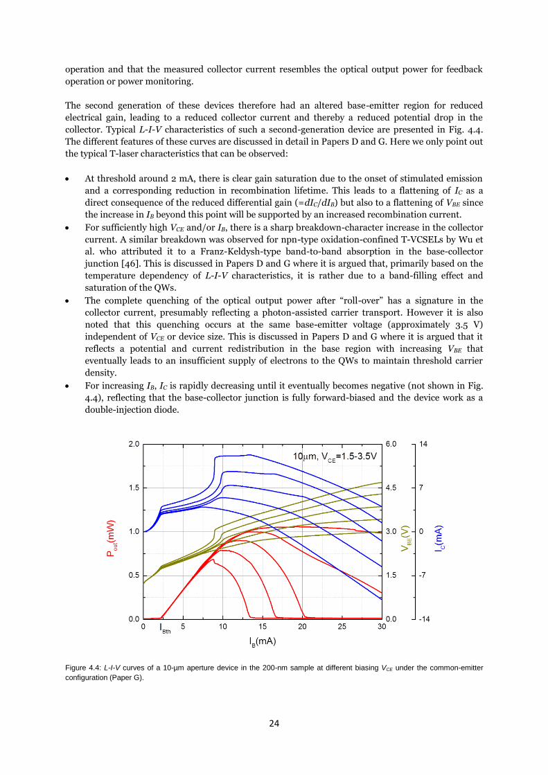
The second generation of these devices therefore had an altered base-emitter region for reduced
electrical gain, leading to a reduced collector current and thereby a reduced potential drop in the
collector. Typical L-I-V characteristics of such a second-generation device are presented in Fig. 4.4.
The different features of these curves are discussed in detail in Papers D and G. Here we only point out
the typical T-laser characteristics that can be observed:
At threshold around 2 mA, there is clear gain saturation due to the onset of stimulated emission
and a corresponding reduction in recombination lifetime. This leads to a flattening of IC as a
direct consequence of the reduced differential gain (=dIC/dIB) but also to a flattening of VBE since
the increase in IB beyond this point will be supported by an increased recombination current.
For sufficiently high VCE and/or IB, there is a sharp breakdown-character increase in the collector
current. A similar breakdown was observed for npn-type oxidation-confined T-VCSELs by Wu et
al. who attributed it to a Franz-Keldysh-type band-to-band absorption in the base-collector
junction [46]. This is discussed in Papers D and G where it is argued that, primarily based on the
temperature dependency of L-I-V characteristics, it is rather due to a band-filling effect and
saturation of the QWs.
The complete quenching of the optical output power after “roll-over” has a signature in the
collector current, presumably reflecting a photon-assisted carrier transport. However it is also
noted that this quenching occurs at the same base-emitter voltage (approximately 3.5 V)
independent of VCE or device size. This is discussed in Papers D and G where it is argued that it
reflects a potential and current redistribution in the base region with increasing VBE that
eventually leads to an insufficient supply of electrons to the QWs to maintain threshold carrier
density.
For increasing IB, IC is rapidly decreasing until it eventually becomes negative (not shown in Fig.
4.4), reflecting that the base-collector junction is fully forward-biased and the device work as a
double-injection diode.
Figure 4.4: L-I-V curves of a 10-µm aperture device in the 200-nm sample at different biasing VCE under the common-emitter
configuration (Paper G).

25
Typical electrical and optical common-emitter collector diagrams are shown in Fig. 4.5. The dash lines
indicate a lower base potential than the collector (VBC < 0) measured at the terminals based on the VBE-
vs-VCE results which is not presented here but follows the same trend as the IC-vs-VCE diagram since
VBE depends on IE (=IC+IB) and IB is kept constant. The solid lines correspond to the situation when the
measured base terminal potential is higher than the collector terminal (VBC > 0). Meanwhile, black
color indicates that only spontaneous emission is observed and red color suggests the stimulated
emission. The VCE offset voltage increases with a higher IB and the VCE biasing at VBC = 0 is located in
the active region of the collector diagram given a certain IB, indicated as the transition point from dash
line to soild line, both of which is attributed to voltage drops induced by layer resistances. The gain
compression at threshold is clearly observed as a denser distribution of lines in the IC-vs-VCE diagram
for a constant increment in IB. The breakdown in IC, matching the quenching of Pout, is observed to
occur at decreasing VCE for increasing IB, consistent with the observations in Fig. 4.4. From a closer
inspection (Paper D) it is possible to see a reduction in threshold current in the limit of high VCE
(around 4.5 V) due to direct tunneling of electrons from the collector to the base. An interesting
observation is also that large part of the light emission can be obtained in the transistor saturation
regime (VBC < 0).
Figure 4.5 Collector diagram and voltage-controlled lasing of a 10-µm aperture device in the 200-nm sample at room-
temperature in the common-emitter configuration (Paper G).
The measured results of a 10-µm aperture with asymmetric mesa and 200-nm base doping layer in
comparison to the symmetric mesa design are demonstrated in Fig. 4.6. Despite a similar IBth and
current gain, VBE increases much faster in the case of the asymmetric mesa, indicating a higher
effective cavity resistance as a result of a non-uniform current injection. Besides, the optical output
power is only 60% as compared to the symmetric mesa design for the same aperture size. This suggests
a carrier-gain mismatch induced by the non-uniform injection profile.

26
Figure 4.6 Measurement results of VBE (top) and IC (bottom) as function of IB of a 10-µm aperture T-VCSEL with asymmetric and
symmetric mesa designs.
4.3 Results of tunnel-junction confined T-VCSELs
Buried tunnel-junction (BTJ) devices were first evaluated in conventional diode-VCSELs and despite
the non-optimized tunnel junction a clear reduction of the parasitic contributions were obtained
[Paper F]. For the T-VCSELs, both of GaAs (p-type)/InGaAs (n-type) and InGaAs (p-type)/InGaAs (n-
type) were implemented, where the latter type would be expected to show an even reduced voltage
drop and series resistance. Figure 4.7 shows measured L-I-V characteristics from a 10-µm aperture
BTJ-T-VCSEL with standard symmetric mesa design. Compared to the results of a similar device with
pn-blocking layer confinement scheme, a much lower current gain and Pout along with a higher VBE are
obtained from the BTJ-T-VCSEL, which at first sight appears counter-intuitive. The measured results
indicate that the tunnel-junction provides higher resistance than expected thereby yielding a higher
VBE.

27
Figure 4.7 L-I-V characteristics of a 10-µm aperture T-VCSEL with symmetric mesa and InGaAs/InGaAs buried tunnel-junction
designs.

28
5. Summary and outlook
5.1 Conclusions
In this thesis, a new optoelectronics device, the T-VCSEL, has been examined both theoretically and
experimentally. Comprehensive three-dimensional numerical simulations taking account of electrical,
optical and thermal properties has been used for device design, optimization and performance
predictions, and several generations of prototypical GaAs-based T-VCSELs have been fabricated and
analyzed. The work and results can be summarized as follows:
A T-VCSEL biased in the common-base configuration may have a modulation bandwidth
surpassing those of conventional diode-VCSELs or T-VCSELs biased in the common-emitter
configuration.
Several generations of GaAs-based T-VCSELs were designed, fabricated and analyzed. The design
makes use of an epitaxial regrowth process including triple-intracavity contacting, undoped DBRs
and modulation doping for minimized optical loss. This resulted in the first demonstration of T-
VCSELs operating continuous-wave at room-temperature and beyond with static performance
figures resembling those of conventional diode VCSELs in terms of threshold current, output
power, power efficiency and high-temperature operation.
The collector current breakdown mechanism, in previous works identified as a Franz-Keldysh-
photon reabsorption process [46], was analyzed in some detail and it was concluded that the
governing mechanism behind this breakdown rather is related to a band-filling effect.
Different design variations for an efficient current injection based on epitaxially regrown pn-
blocking layers, a BTJ and/or an asymmetric device layout for improved lateral feeding were
investigated. The BTJ concept corresponds to a simplified processing sequence and reduced
parasitics and should be of interest for further optimizations, whereas the asymmetric current
injection resulted in reduced power, increased threshold and reduced operation range. This may
very well have the potential for improvement using better optimized contact layout and/or layer
structure.
5.2 Suggestions for future work
The T-VCSEL is still in a very early stage of development. While the present study represents the first
successful demonstration of the room-temperature operation of such devices, there is a long way to go
before it becomes clear whether it can have any impact on applications, e.g., in high-speed data
communication as frequently suggested in literature. This will correspond to a cumbersome step-by-
step approach to evaluate different design approaches for optimized static performance, dynamic
measurement to evaluate intrinsic and extrinsic bandwidth limitations, noise properties linearity,
feedback-operation, etc. Equivalent circuit models need to be constructed to evaluate the potential for
using it as building blocks in more advanced configurations that for instance taking account of
transistor-based design techniques to realize compact circuits for microwave applications. The most
immediate concerns will be to evaluate design-improvements for the here presented devices in terms
of static and dynamic properties:
The optimization and implementation of improved BTJ structures. Using the present n+p+
InGaAs/(In)GaAs as a base line other heterojunctions for more efficient tunneling should be
evaluated. This may include higher In-content or increased-doping InGaAs/InGaAs junctions but
also more novel varieties such as (In)GaAs(Sb):p++/(In)GaAs(N):n++ junction for where Sb and N
have the effects of pushing up the valence band edge and pushing down the conduction band edge,
respectively [67]. However, it is important to note that the tunnel junction needs to be designed in

29
such a way that band-to-band absorption of the lasing light should be avoided. This approach has
so far been more common for long-wavelength VCSELs in the 1100 to 1550-nm regime [7, 16, 68].
Theoretical and experimental investigations on an altered layer structure and lateral device design
to meet the combined requirements on a short-cavity with functional transistor operation.
Further investigations and optimization of p-doped cavity/active layer regions for preserved
luminescence properties so that also npn-type T-VCSELs can be examined.
Extensive dynamic characterizations to explore the bandwidth limitations and construction of
equivalent circuit models.
Refined theoretical models to enable a more thorough understanding of ultimate performance
limitations.
Identifications and investigations of different applications that may benefit from the T-VCSEL, e.g.
taking account of the three-terminal configuration for signal-mixing, collector current-based
feedback operation or the potentially extended dynamic properties.

30
Guide to the papers
Paper A: Design and modeling of a transistor vertical-cavity surface-emitting
laser A numerical model of npn T-VCSEL is established, incorporating various physical models to describe
important effects such as Coulomb enhancement, free-carrier absorption, Auger recombination, QW
capture/escape process, etc. The material parameters and coefficients are carefully calibrated against
the photoluminescence results of InGaAs QWs as well as L-I-V curves of a conventional GaAs-based
VCSEL with otherwise similar design as the here considered T-VCSEL. Both the static performance
and modulation response are derived based on the simulation, which demonstrate the influence of
quantum capture/escape process on electrical and optical properties and the modulation bandwidth
enhancement in the common-base configuration.
Author contribution: part of 980-nm VCSEL design and growth, discussions on the analysis and
modeling
Paper B: Room-temperature operation of a transistor vertical-cavity surface-
emitting laser A GaAs-based 980-nm pnp T-VCSEL working at room-temperature up to 50°C is demonstrated for the
first time. A pn-blocking layer is implemented during two regrowth steps as the electrical and optical
confinement scheme. Square active regions and mesas are defined and a Si/SiO2 dielectric top DBR is
deposited. The device is operated in current and voltage controlled modes, with mA-level threshold
current and mW-range optical power.
Author contribution: Part of the device design and fabrication, characterization, data analysis
Paper C: Minority current distribution in InGaAs/GaAs transistor-vertical-cavity
surface-emitting laser The static performance of the T-VCSELs demonstrated in Paper A is examined using numerical
simulations. It is found that the internal potential and carrier distribiutions have a large impact on the
device performance, e.g. leading to a premature saturation below threshold. As a result, it operates in
the active mode in the interior of the device while the measured current-voltage characteristics
indicate that it is in saturation.
Author contribution: Device characterization, simulation, data analysis, writing the paper
Paper D: Performance optimization of GaAs-based pnp-type vertical-cavity
surface-emitting transistor-lasers GaAs-based pnp T-VCSELs are fabricated with systematic variation of the base width. It is
demonstrated that the active mode of operation can be extended by an increased base width due to the
combined effects of reduced base resistance and current gain. This results in transistor-laser like
characteristics well beyond lasing threshold, including mA-range threshold current, mW-range
outpout power, record-low power dissipation during lasing and high-temperature lasing up to at least
60°C. The collector current breakdown characteristics as function of base current or emitter-collector
voltage is studied in some detail and in contrast to previous studies it is suggested that the breakdown
mechanism presumably is trigged by a quantum band-filling effect.
Author contribution: Device design and fabrication, characterization, data analysis, writing the paper

31
Paper E: Influence of base-region thickness on the performance of pnp
transistor-VCSEL Numerical multi-physics device simulations are performed in order to better understand the device
physics of the first generation T-VCSELs (presented in Papers B and C) and as a tool for device
optimization. The simulations suggest that the operating range of the T-VCSEL can be enhanced from
an extension of the base width, which was later confirmed by measurements on fabricated devices
(Paper D). Guidelines are also provided regarding the doping distribution in the base region and the
positioning of the quantum wells, and it is suggested that alternative device designs that allow the
positioning of the metal contacts closer to the center of the device should be evaluated.
Author contribution: Device fabrication and characterization, part of the simulation optimization
Paper F: 1.3-µm buried tunnel junction InGaAs/GaAs VCSELs InGaAs/GaAs VCSELs are fabricated using an epitaxial regrowth process. Using highly strained
InGaAs/GaAs QWs with emission wavelength beyond 1200-nm in combination with a negative gain-
cavity detuning, it is possible to extend the wavelength towards 1300-nm. Pn-blocking layer and
buried tunnel-junction confinement are compared and it is concluded that the latter can provide lower
series resitance and improved high-speed dynamics through a reduction of the electrical parasitics.
Author contribution: Part of the device design and fabrication, characterization
Paper G: AlGaAs/GaAs/InGaAs pnp-type vertical-cavity surface-emitting
transistor-lasers The fabrication and optimization of pnp-type T-VCSELs are reviewed. Measurements on T-VCSELs
with systematic design variations reveal a rich interplay between electrical field, current distribution
and optical field that needs to be taken into account in the optimization process. Tunnel-juntion
current injection and devices with asymmetric contact layeout are investigated for the purpose of
reducing the extrinsic base, emitter and collector resistances.
Author contribution: Device design and fabrication, characterization, data analysis, writing the paper

32
References
[1] H. Soda, K.-i. Iga, C. Kitahara and Y. Suematsu, "GaInAsP/InP Surface Emitting Injection Lasers," Jpn. J. Appl.
Phy, vol. 18, no. 12, p. 2329, 1979.
[2] R. Michalzik edited, VCSELs: Fundamentals, Technology and Applications of Vertical-Cavity Surface-
Emitting Lasers, Springer, 2013.
[3] J. K. Guenter, R. A. H. III, D. N. Granville, M. K. Hibbs-Brenner and R. A. Morgan, "Reliability of proton-
implanted VCSELs for data communications," in Photonics West, International Society for Optics and
Photonics, 1996.
[4] P. Westbergh, R. Safaisini, E. Haglund, J. S. Gustavsson, A. Larsson and A. Joel, "High-speed 850 nm VCSELs
with 28 GHz modulation bandwidth for short reach communication," in SPIE OPTO. International Society
for Optics and Photonics, 2013.
[5] P.Wolf, P. Moser, G. Larisch, M. Kroh, A. Mutig, W. Unrau, W. Hofmann and D. Bimberg, "High-
performance 980 nm VCSELs for 12.5 Gbit/s data transmission at 155°C and 49 Gbit/s at −14°C," Electronic
Letters, vol. 48, no. 7, pp. 389-390, 2012.
[6] M. Müller, C. Grasse and M. C. Amann, "InP-based 1.3 μm and 1.55 μm short-cavity VCSELs suitable for
telecom-and datacom-applications," in Transparent Optical Networks (ICTON), 2012 14th International
Conference on, 2012.
[7] W. Hofmann, M. Müller, P. Wolf, A. Mutig, T. Gründl, G. Böhm, D. Bimberg and M. C. Amann, "40 Gbit/s
modulation of 1550 nm VCSEL," Electronics Letters, vol. 47, no. 4, pp. 270-271, 2011.
[8] D. Kuchta, A. V. Rylyakov, C. L. Schow, J. Proesel, C. Baks, P. Westbergh, J. S. Gustavsson and A. Larsson,
"64Gb/s Transmission over 57m MMF using an NRZ Modulated 850nm VCSEL," in Optical Fiber
Communication Conference, 2014.
[9] D. M. Kuchta, A. V. Rylyakov, C. L. Schow, J. E. Proesel, C. Baks, C. Kocot, L. Graham, R. Johnson, G. Landry,
E. Shaw, A. MacInnes and J. Tatum, "A 55Gb/s Directly Modulated 850nm VCSEL-Based Optical Link," in
Photonics Conference (IPC), 2012 IEEE, 2012.
[10] M. Chaciński, N. Chitica, S. Molin, N. Lalic and O. Sahlén, "25.78Gbps Data Transmission with 850nm
Multimode VCSEL Packaged in QSFP Form Factor Module," in Optical Fiber Communication Conference,
2013.
[11] S. Blokhin, J. Lott, A. Mutig, G. Fiol, N. Ledentsov, M. Maximov, A. Nadtochiy, V. Shchukin and D. Bimberg,
"Oxide-confined 850 nm VCSELs operating at bit rates up to 40 Gbit/s," Electronics Letters, vol. 45, no. 10,
pp. 501-503, 2009.
[12] J. Wang, M. Keever, Z.-W. Feng, T. Fanning, C. Chu, A. Sridhara, F. Hopfer, T. Sale, A.-N. Cheng, B. Shao, L.
Ding, P. Wen, H.-H. Chang, C. Wang, D. C. W. Hui and L. Giovane, "28 Gb/s 850 nm oxide VCSEL
development at Avago," in SPIE OPTO. International Society for Optics and Photonics, 2013.
[13] M. Grabherr, S. Intemann, S. Wabra, P. Gerlach, M. Riedl and R. King, "25 Gbps and beyond: VCSEL

33
development at Philips," in SPIE OPTO. International Society for Optics and Photonics, 2013.
[14] N. Li, C. Xie, W. Luo, C. J. Helms, L. Wang, C. Liu, Q. Sun, S. Huang, C. Lei, K. P. Jackson and R. F. Carson,
"Emcore's 1 Gb/s to 25 Gb/s VCSELs," in SPIE OPTO. International Society for Optics and Photonics, 2012.
[15] T. Suzuki, S. Imai, S. Kamiya, K. Hiraiwa, M. Funabashi, Y. Kawakita, H. Shimizu, T. Ishikawa and A.
Kasukawa, "Reliability study of 1060nm 25Gbps VCSEL in terms of high speed modulation," in SPIE OPTO.
International Society for Optics and Photonics, 2012.
[16] M. Müller, P. Wolf, C. Grasse, M. Dias, M. Ortsiefer, G. Böhm, E. Wong, W. Hofmann, D. Bimberg and M.-C.
Amann, "1.3 µm short-cavity VCSELs enabling error-free transmission at 25 Gbit/s over 25 km fibre link,"
Electronics Letters , vol. 48, no. 23, pp. 1487-1489, 2012.
[17] A. Larsson, J. Gustavsson, Å. Haglund and P. Westbergh, "Advances in VCSELs for communication and
sensing," in Semiconductor Laser Conference (ISLC), 2010 22nd IEEE International. IEEE, 2010.
[18] A. Paraskevopoulos, H.-J. Hensel, W.-D. Molzow, H. Klein, N. Grote, N. Ledentsov, V. Shchukin, C. Möller, A.
Kovsh, D. Livshits, I. Krestnikov, S. Mikhrin, P. Matthijsse and G. Kuyt, "Ultra-High-Bandwidth (>35 GHz)
Electrooptically-Modulated VCSEL," in Optical Fiber Communication Conference, 2006.
[19] L. Chrostowski, X. Zhao, C. J. Chang-Hasnain, R. Shau, M. Ortsiefer and M.-C. Amann, "50-GHz Optically
Injection-Locked 1.55-μm VCSELs," IEEE Photonics Technol. Lett., vol. 18, no. 2, pp. 367-369, 2006.
[20] H. Dalir and F. Koyama, "High-speed operation of bow-tie-shaped oxide aperture VCSELs with photon–
photon resonance," Appl. Phys. Expr., vol. 7, no. 2, p. 022102, 2014.
[21] I.-S. Chung and J. Mørk, "Speed enhancement in VCSELs employing grating mirrors," in SPIE OPTO.
International Society for Optics and Photonics, 2013.
[22] K. Szczerba, B.-E. Olsson, P. Westbergh, A. Rhodin, J. Gustavsson, Å. Haglund, M. Karlsson, A. Larsson and
P. A. Andrekson, "37 Gbps transmission over 200 m of MMF using single cycle subcarrier modulation and a
VCSEL with 20 GHz modulation bandwidth," in 2010 36th European Conference and Exhibition on Optical
Communication (ECOC), 2010.
[23] M. Feng, N. Holonyak and R. Chan, "Quantum-well-base heterojunction bipolar light-emitting transistor,"
Applied Physics Letters, vol. 84, no. 11, pp. 1952-1954, 2004.
[24] H. W. Then, M. Feng and N. Holonyak, "Optical bandwidth enhancement by operation and modulation of
the first excited state of a transistor laser," Applied Physics Letters, vol. 91, no. 18, p. 183505, 2007.
[25] M. Feng, N. Holonyak, G. Walter and R. Chan, "Room temperature continuous wave operation of a
heterojunction bipolar transistor laser," Applied Physics Letters, vol. 87, no. 13, p. 131103, 2005.
[26] [Online]. Available: http://phys.org/news68731792.html.
[27] Y. Mori, J. Shibata, Y. Sasai, H. Serizawa and T. Kajiwara, "Operation principle of the InGaAsP/InP laser
transistor," Applied Physics Letters, vol. 47, no. 7, pp. 649-651, 1985.
[28] M. Shirao, T. Sato, N. Sato, N. Nishiyama and S. Arai, "Room-temperature operation of npn- AlGaInAs/InP
multiple quantum well transistor laser emitting at 1.3-µm wavelength," Optics Express, vol. 20, no. 4, pp.

34
3983-3989, 2012.
[29] Z. Duan, W. Shi, L. Chrostowski, X. Huang, N. Zhou and G. Chai, "Design and epitaxy of 1.5 μm InGaAsP-InP
MQW material for a transistor laser," Optics Express, vol. 18, no. 2, pp. 1501-1509, 2010.
[30] S. Liang, D. H. Kong, H. L. Zhu, L. J. Zhao, J. Q. Pan and W. Wang, "InP-based deep-ridge NPN transistor
laser," Optics Letters, vol. 36, no. 16, pp. 3206-3208, 2011.
[31] B. Faraji, W. Shi, D. L. Pulfrey and L. Chrostowski, "Analytical Modeling of the Transistor Laser," IEEE
Journal of Selected Topics in Quantum Electronics, vol. 15, no. 3, pp. 594-603, 2009.
[32] M. Shirao, S. Lee, N. Nishiyama and S. Arai, "Large-Signal Analysis of a Transistor Laser," IEEE JOURNAL OF
QUANTUM ELECTRONICS, vol. 47, no. 3, pp. 359-367, 2011.
[33] I. Taghavi, H. Kaatuzian and J.-P. Leburton, "Bandwidth enhancement and optical performances of multiple
quantum well transistor lasers," Applied physics letters, vol. 100, no. 23, p. 231114, 2012.
[34] H. W. Then, M. Feng and N. Holonyak, "Physics of base charge dynamics in the three port transistor laser,"
Applied Physics Letters, vol. 96, no. 11, p. 113509, 2010.
[35] M. Feng, H. W. Then, N. Holonyak, G. Walter and A. James, "Resonance-free frequency response of a
semiconductor laser," Applied Physics Letters, vol. 95, no. 3, p. 033509, 2009.
[36] F. Tan, R. Bambery, M. Feng and N. Holonyak, "Relative intensity noise of a quantum well transistor laser,"
Applied Physics Letters, vol. 10, no. 15, p. 151118, 2012.
[37] H. W. Then, F. Tan, M. Feng and N. Holonyak, "Transistor laser optical and electrical linearity enhancement
with collector current feedback," Applied Physics Letters, vol. 100, no. 22, p. 221104, 2012.
[38] E. W. Iverson and M. Feng, "Transistor Laser Power Stabilization Using Direct Collector Current Feedback
Control," IEEE PHOTONICS TECHNOLOGY LETTERS, vol. 24, no. 1, pp. 4-6, 2012.
[39] B. Faraji, W. Shi, D. L. Pulfrey and L. Chrostowski, "Common-emitter and common-base small-signal
operation of the transistor laser," Applied Physics Letters, vol. 93, no. 14, p. 143503, 2008.
[40] W. Shi, L. Chrostowski and B. Faraji, "Numerical study of the optical saturation and voltage control of a
transistor vertical-cavity surface-emitting laser," IEEE Photonics Technology Letters, vol. 20, no. 24, pp.
2141-2143, 2008.
[41] R. Bambery, F. Tan, M. Feng, J. M. Dallesasse and N. Holonyak, "Voltage and Current Modulation at 20
Gb/s of a Transistor Laser at Room Temperature," IEEE Photonics Technology Letters, vol. 25, no. 9, pp.
859-862, 2013.
[42] H. W. Then, C. H. Wu, G. Walter, M. Feng and N. Holonyak, "Electrical-optical signal mixing and
multiplication (2→22 GHz) with a tunnel junction transistor laser," Applied Physics Letters, vol. 94, no. 10,
p. 10114, 2009.
[43] W. Liu, Fundamentals of III-V devices: HBTs, MESFETs, and HEMTs, Wiley-Interscience, 1999.
[44] B. Faraji, Modeling of the Transistor Vertical Cavity Surface Emitting Laser, Ph.D. Thesis, University of

35
British Columbia, 2011.
[45] M.-K. Wu, M. Feng and N. Holonyak, "Surface Emission Vertical Cavity Transistor Laser," IEEE Photonics
Technology Letters, vol. 24, no. 15, pp. 1346-1348, 2012.
[46] M. K. Wu, M. Feng and N. Holonyak, "Voltage modulation of a vertical cavity transistor laser via intra-
cavity photon-assisted tunneling," Applied Physics Letters, vol. 101, no. 8, p. 081102, 2012.
[47] [Online]. Available: http://www.electrumlaboratoriet.se/KTHAcreo.aspx.
[48] R. Marcks von Würtemberg, X. Yu, J. Berggren and M. Hammar, "Performance optimisation of epitaxially
regrown 1.3-µm vertical-cavity surface-emitting lasers," IET Optoelectronics, vol. 3, no. 2, pp. 112-121,
2009.
[49] G. Walter, N. Holonyak, M. Feng and R. Chan, "Laser operation of a heterojunction bipolar light-emitting
transistor," Applied Physics Letters, vol. 85, no. 20, pp. 4768-4770, 2004.
[50] C. Asplund, S. Mogg, G. Plaine, F. Salomonsson, N. Chitica and M. Hammar, "Doping-induced losses in
AlAs/GaAs distributed Bragg reflectors," Journal of Applied Physics, vol. 90, no. 2, pp. 794-800, 2001.
[51] M.-K. Wu, M. Liu, R. Bambery, M. Feng and N. Holonyak, "Low Power Operation of a Vertical Cavity
Transistor Laser via the Reduction of Collector Offset Voltage," IEEE Photonics Technology Letters, vol. 26,
no. 10, pp. 1003-1006, 2014.
[52] [Online]. Available: www.crosslight.com.
[53] X. Wu, Simulation Study of Epitaxially Regrown Vertical-Cavity Surface-Emitting Lasers, Master Thesis,
Royal Institute of Technology, 2011.
[54] S. M. Sze and K. K. Ng, Physics of Semiconductor Devices, 3rd Edition, Wiley, 2006.
[55] E. M. Azoff, "Energy Transport Numerical Simulation of Graded AlGaAs/GaAs Heterojunction Bipolar
Transis tors," IEEE Transactions on Electron Devices, vol. 36, no. 4, pp. 609-616, 1989.
[56] E. M. Azoff, "Close-form method for solving the steady-state generalized energy-momentum conservation
equations," COMPEL - The international journal for computation and mathematics in electrical and
electronic engineering, vol. 6, no. 1, pp. 25-30, 1987.
[57] M. A. Alam, "Simulation of semiconductor quantum well lasers," IEEE Transactions on Electron Devices,
vol. 47, no. 10, pp. 1917-1925, 2000.
[58] E. Snitzer, "Cylindrical Dielectric Waveguide Modes," Journal of the Optical Societ of America, vol. 51, no.
5, pp. 491-498, 1961.
[59] G. R. Hadley, K. L. Lear, M. E. Warren, K. D. Choquette, J. W. Scott and S. W. Corzine, "Comprehensive
Numerical Modeling of Vertical-Cavity Surface-Emitting Lasers," IEEE Journal of Quantum Electronics, vol.
32, no. 4, pp. 607-616, 1996.
[60] S. R. Chinn, P. S. Zory and A. R. Reisinger, "A Model for GRIN-SCH-SQW Diode Lasers," IEEE Journal of
Quantum Electronics, vol. 24, no. 11, pp. 2191-2214, 1988.

36
[61] C.-F. Hsu, P. S. Zory, C.-H. Wu and M. A. Emanuel, "Coulomb enhancement in InGaAs-GaAs quantum-well
lasers," Selected Topics in Quantum Electronics, vol. 3, no. 2, pp. 158-165, 1997.
[62] H. Kroemer, "Heterostructure Bipolar Transistors and Integrated Circuits," Proceedings of the IEEE, vol. 70,
no. 1, pp. 13-25, 1982.
[63] N. Pan, J. Elliott, M. Knowles, D. P. Vu, K. Kishimoto, J. K. Twynam, H. Sato, M. T. Fresina and G. E. Stillman,
"High Reliability InGaP/GaAs HBT," IEEE Electron Device Letters, vol. 19, no. 4, pp. 115-117, 1998.
[64] Y. Huang, J.-H. Ryou and R. D. Dupuis, "Control of Zn diffusion in InP/InAlGaAs-based heterojunction
bipolar transistors and light emitting transistors," Journal of Crystal Growth, vol. 310, no. 19, pp. 4345-
4350, 2008.
[65] M. Feng, N. Holonyak, G. Walter and R. Chan, "Room temperature continuous wave operation of a
heterojunction bipolar transistor laser," Applied Physics Letters, vol. 87, no. 13, p. 131103, 2005.
[66] R. King, Philips Photonics, private communication.
[67] I. Vurgaftman, J. R. Meyer and L. R. Ram-Mohan, "Band parameters for III–V compound semiconductors
and their alloys," Journal of Applied Physics, vol. 89, no. 11, pp. 5815-5875, 2001.
[68] K. Yashiki, N. Suzuki, K. Fukatsu, T. Anan, H. Hatakeyama and M. Tsuji, "1.1-μm-Range Tunnel Junction
VCSELs with 27-GHz Relaxation Oscillation Frequency," in Optical Fiber Communication Conference, Optical
Society of America, 2007.

37
Appendix I: Processing list of T-VCSEL
1. Epitaxy 1.1 Growth according to layer configuration
2. Regrowth
2.1 Deposition of SiO2 and Si3N4
2.1.1 HCl: H2O=1: 2, 30sec, rinse in DI-H2O
2.1.2 Deposition of 100-nm SiO2 in Pekka: 300°C, 90sec
2.1.3 Deposition of 60-nm Si3N4, in Pekka: 300°C, 250sec
2.2 Lithography of aperture 1
2.2.1 HMDS, 25min
2.2.2 Spinning: SPR700-1.2, 4000rpm, 30sec
2.2.3 Contact hotplate: 95°C, 60sec
2.2.4 DSW stepper: ex xiangact1\1,2,3,4,5, exposure 0.3sec on patterns and 0.35sec on blank edges
2.2.5 Contact hotplate: 115°C, 60sec
2.2.6 Develop: CD-26, 32sec
2.2.7 Rinse in bubble water, 60sec
2.3 Si3N4 etch
2.3.1 Ash in ESA: 15mTorr, 45W, 25sccm O2, 30sec
2.3.2 Etch in ESA: 15mTorr, 45W, 25sccm CF4, 7min
2.3.3 Ash in ESA: 15mTorr, 45W, 25sccm O2, 2min
2.4 Removal of resist
2.4.1 Acetone + propanol + H2O, 5min + 5min + 5min
2.4.2 Ash in ESA: 15mTorr, 45W, 25sccm O2, 30sec
2.5 Lithography of aperture 2
2.5.1 HMDS, 25min
2.5.2 Spinning: SPR700-1.2, 4000rpm, 30sec
2.5.3 Contact hotplate: 95°C, 60sec
2.5.4 DSW stepper: map xiangact2\mapreg,1,2,3,4,5, exposure 0.3sec on patterns and 0.35sec on
blank edges
2.5.5 Contact hotplate: 115°C, 60sec
2.5.6 Develop: CD-26, 32sec
2.5.7 Rinse in bubble water, 60sec
2.6 Si3N4 etch
2.6.1 Ash in ESA: 15mTorr, 45W, 25sccm O2, 30sec
2.6.2 Etch in ESA: 15mTorr, 45W, 25sccm CF4, 7min
2.6.3 Ash in ESA: 15mTorr, 45W, 25sccm O2, 2min
2.7 Removal of resist
2.7.1 Acetone + propanol + H2O, 5min + 5min + 5min
2.7.2 Ash in ESA: 15mTorr, 45W, 25sccm O2, 30sec
2.8 SiO2 etch
2.8.1 BHF: H2O=1: 25, 2min30sec
2.9 GaAs wet etch (in the case of pn-blocking T-VCSEL)
2.9.1 Si3N4 etch in ESA: 150mTorr, 30W, 45sccm CF4, 5sccm O2, 3min
2.9.2 HCl: H2O=1: 2, 2min30sec
2.9.3 GaAs wet etch: H2O: NH4OH: H2O2=1000: 20: 7
2.9 GaAs wet etch (in the case of tunnel junction T-VCSEL)
2.9.1 HCl: H2O=1: 2, 2min30sec
2.9.2 GaAs wet etch: H2O: NH4OH: H2O2=1000: 20: 7
2.10 Regrowth (in the case of pn-blocking T-VCSEL)
2.10.1 Regrowth of blocking layer
38
2.10.2 SiO2 etch: BHF, 30sec
2.10.3 2nd regrowth of conducting layer
2.10 Regrowth (in the case of tunnel junction T-VCSEL)
2.10.1 Si3N4 and SiO2 etch: BHF, 30sec
2.10.2 Regrowth of conducting layer
3. Base mesa define
3.1 Deposition of SiO2
3.1.1 Deposit 200-nm SiO2 in Pekka: 300°C, 180sec
3.2 Lithography of base mesa
3.2.1 HMDS, 25min
3.2.2 Spinning: SPR700-1.2, 4000rpm, 30sec
3.2.3 Contact hotplate: 95°C, 60sec
3.2.4 DSW stepper: map xiangbpit\mapreg,1,2,3,4,5, exposure 0.3sec on patterns and 0.35sec on
blank edges
3.2.5 Contact hotplate: 115°C, 60sec
3.2.6 Develop: CD-26, 32sec
3.2.7 Rinse in bubble water, 60sec
3.3 SiO2 etch
3.3.1 Ash in ESA: 15mTorr, 45W, 25sccm O2, 30sec
3.3.2 BHF: H2O=1: 25, 5min
3.4 GaAs dry etch
3.4.1 RIE in Fabio: 2mTorr, SiCl4 = 3sccm, Ar = 2sccm, power = 40W
3.5 Remove of resist
3.5.1 Ash in ESA: 15mTorr, 45W, 25sccm O2, 2min
3.5.2 Acetone + propanol + H2O, 5min + 5min + 5min
3.5.3 Ash in ESA: 15mTorr, 45W, 25sccm O2, 30sec
3.6 GaAs wet etch
3.6.1 GaAs wet etch: H2O: NH4OH: H2O2=1000: 20: 7
3.7 SiO2 etch
3.7.1 BHF, 30sec
4. Collector mesa define
4.1 Deposition of SiO2
4.1.1 Deposit 200-nm SiO2 in Pekka: 300°C, 180sec
4.2 Lithography of collector mesa
4.2.1 HMDS, 25min
4.2.2 Spinning: SPR700-1.2, 4000rpm, 30sec
4.2.3 Contact hotplate: 95°C, 60sec
4.2.4 DSW stepper: map xiangcpit\mappit,1,2,3,4,5, exposure 0.3sec on patterns and 0.35sec on blank
edges
4.2.5 Contact hotplate: 115°C, 60sec
4.2.6 Develop: CD-26, 32sec
4.2.7 Rinse in bubble water, 60sec
4.3 SiO2 etch
4.3.1 Ash in ESA: 15mTorr, 45W, 25sccm O2, 30sec
4.3.2 BHF: H2O=1: 25, 5min
4.4 GaAs dry etch
4.4.1 RIE in Fabio: 2mTorr, SiCl4 = 3sccm, Ar = 2sccm, power = 40W
4.5 Remove of resist
4.5.1 Ash in ESA: 15mTorr, 45W, 25sccm O2, 2min
4.5.2 Acetone + propanol + H2O, 5min + 5min + 5min
4.5.3 Ash in ESA: 15mTorr, 45W, 25sccm O2, 30sec

39
4.6 GaAs wet etch
4.6.1 GaAs wet etch: H2O: NH4OH: H2O2=1000: 20: 7
4.7 SiO2 etch
4.7.1 BHF, 30sec
5. TLM mesa define
5.1 Deposition of SiO2
5.1.1 Deposit 200-nm SiO2 in Pekka: 300°C, 180sec
5.2 Lithography of TLM mesa
5.2.1 HMDS, 25min
5.2.2 Spinning: SPR700-1.2, 4000rpm, 30sec
5.2.3 Contact hotplate: 95°C, 60sec
5.2.4 DSW stepper: map xiangtlm\mapreg,1, exposure 0.3sec
5.2.5 Contact hotplate: 115°C, 60sec
5.2.6 Develop: CD-26, 32sec
5.2.7 Rinse in bubble water, 60sec
5.3 SiO2 etch
5.3.1 Ash in ESA: 15mTorr, 45W, 25sccm O2, 30sec
5.3.2 BHF: H2O=1: 25, 5min
5.4 GaAs dry etch
5.4.1 RIE in Fabio: 2mTorr, SiCl4 = 3sccm, Ar = 2sccm, power = 40W
5.5 Remove of resist
5.5.1 Ash in ESA: 15mTorr, 45W, 25sccm O2, 2min
5.5.2 Acetone + propanol + H2O, 5min + 5min + 5min
5.5.3 Ash in ESA: 15mTorr, 45W, 25sccm O2, 30sec
5.6 SiO2 etch
5.6.1 BHF, 30sec
6. N-type contact deposition
6.1 Si3N4 deposition
6.1.1 Deposit 135-nm SiO2 in Pekka: CIP21, 25min
6.2 Lithography of N-metal
6.2.1 HMDS, 25min
6.2.2 Spinning: S1818, 4000rpm, 30sec
6.2.3 Contact hotplate: 115°C, 60sec
6.2.4 DSW stepper: map xiangnmp\mappit,1 (for pn-blocking T-VCSEL) ; mapxiangnmp2\mappit,1
(for tunnel junction T-VCSEL)
6.2.5 Develop: 351: H2O=1: 5, 50sec
6.2.6 Rinse in bubble water, 60sec
6.3 Si3N4 etch
6.3.1 Ash in ESA: 15mTorr, 45W, 25sccm O2, 30sec
6.3.2 Etch in ESA: 15mTorr, 45W, 25sccm CF4, 5sccm O2, 260sec
6.3.3 Etch in ESA: 150mTorr, 25W, 50sccm CF4, 5sccm O2, 150sec
6.3.4 Ash in ESA: 150mTorr, 25W, 50sccm O2, 120sec
6.3.5 HCl: H2O=1: 2, 30sec, rinse in DI-H2O
6.4 Evaporation of N-metal
6.4.1 Evaporation in Barbara: Pd (40nm)/Ge (80nm)/Ti (40nm)/Pd (40nm)/Ti (10nm), from bottom
to top
6.5 Lift-off of N-metal
6.5.1 Lift-off: acetone+ propanol + DI-H2O, 5min + 5min + 5min
6.5.2 Ash in ESA: 15mTorr, 45W, 25sccm O2, 30sec
7. P-type contact deposition

40
7.1 Lithography of P-metal
7.1.1 HMDS, 25min
7.1.2 Spinning: S1818, 4000rpm, 30sec
7.1.3 Contact hotplate: 115°C, 60sec
7.1.4 DSW stepper: map xiangpmp\mapmet,1 (for pn-blocking T-VCSEL); map xiangpmp2\mapmet,1
(for tunnel junction T-VCSEL)
7.1.5 Develop: 351: H2O=1: 5, 50sec
7.1.6 Rinse in bubble water, 60sec
7.2 Si3N4 etch
7.2.1 Ash in ESA: 15mTorr, 45W, 25sccm O2, 30sec
7.2.2 Etch in ESA: 15mTorr, 45W, 25sccm CF4, 5sccm O2, 260sec
7.2.3 Etch in ESA: 150mTorr, 25W, 50sccm CF4, 5sccm O2, 150sec
7.2.4 Ash in ESA: 150mTorr, 25W, 50sccm O2, 120sec
7.2.5 HCl: H2O=1: 2, 30sec, rinse in DI-H2O
7.3 Evaporation of P-metal
7.3.1 Evaporation in Zita and Barbara: Au (5nm)/Zn (30nm)/Au (40nm)/Pd (40nm)/Ti (10nm), from
bottom to top
7.4 Lift-off of P-metal
7.4.1 Lift-off: acetone+ propanol + DI-H2O, 5min + 5min + 5min
7.4.2 Ash in ESA: 15mTorr, 45W, 25sccm O2, 30sec
8. Mirror hole define
8.1 Lithography of mirror hole
8.1.1 HMDS, 25min
8.1.2 Spinning: S1818, 4000rpm, 30sec
8.1.3 Contact hotplate: 115°C, 60sec
8.1.4 DSW stepper: map xiangmirr\mapmet,1
8.1.5 Develop: 351: H2O=1: 5, 50sec
8.1.6 Rinse in bubble water, 60sec
8.2 Si3N4 etch
8.2.1 Ash in ESA: 15mTorr, 45W, 25sccm O2, 30sec
8.2.2 Etch in ESA: 15mTorr, 45W, 25sccm CF4, 5sccm O2, 260sec
8.2.3 Etch in ESA: 150mTorr, 25W, 50sccm CF4, 5sccm O2, 150sec
8.2.4 Ash in ESA: 150mTorr, 25W, 50sccm O2, 120sec
8.3 Remove of resist
8.3.1 Acetone+ propanol + H2O, 5min + 5min + 5min
8.3.2 Ash in ESA: 15mTorr, 45W, 25sccm O2, 30sec
9. Mirror deposition
9.1 Deposit first top mirror layer
9.1.1 Deposit SiO2 in Pekka: 250°C
9.2 Contacts annealing
9.2.1 Annealing in PEO, 325°C, 30min
9.3 Deposit the rest of mirror
9.3.1 Deposit α-Si in P5000: 250°C (×number of periods)
9.3.2 Deposit SiO2 in Pekka: 250°C (×number of periods-1)
10. Via hole
10.1 Lithography of via hole
10.1.1 HMDS, 25min
10.1.2 Spinning: S1818, 4000rpm, 30sec
10.1.3 Contact hotplate: 115°C, 60sec

41
10.1.4 DSW stepper: map xiangvia\mappit,1
10.1.5 Develop: 351: H2O=1: 5, 50sec
10.1.6 Rinse in bubble water, 60sec
10.2 Etch via hole
10.2.1 Ash in ESA: 15mTorr, 45W, 25sccm O2, 30sec
10.2.2 LP α-Si etch in ESA: 25mTorr, 50W, 25sccm CF4, 5sccm O2 (×number of periods)
10.2.3 HP α-Si etch in ESA: 150mTorr, 30W, 50sccm CF4, 5sccm O2 (×number of periods)
10.2.4 SiO2 etch in ESA: 25mTorr, 50W, 25sccm CF4, 5sccm O2 (×number of periods)
10.3 Remove of resist
10.3.1 Ash in ESA: 15mTorr, 45W, 25sccm O2, 2min
10.3.2 Acetone+ propanol + H2O, 5min + 5min + 5min
10.3.3 Ash in ESA: 15mTorr, 45W, 25sccm O2, 30sec
11. Surface metal
11.1 Sputtering of seed layer
11.1.1 Sputter in KDF: TiW, 1.5kW, speed 75, pass 8, 250nm
Au, 1.5kW, speed 200, pass 8, 100nm
11.2 Backside protection
11.2.1 Deposit 200-nm SiO2 in Pekka: 300°C, 180sec
11.3 Lithography of surface metal
11.3.1 HMDS, 25min
11.3.2 Spinning: S1818, 4000rpm, 30sec
11.3.3 Contact hotplate: 115°C, 60sec
11.3.4 DSW stepper: map xiangsup\mappit,1
11.3.5 Develop: 351: H2O=1: 5, 50sec
11.3.6 Rinse in bubble water, 60sec
11.4 Plating of surface metal
11.4.1 Ash in ESA: 15mTorr, 45W, 25sccm O2, 30sec
11.4.2 Plating at Chalmers
11.5 Remove of resist
11.5.1 Ash in ESA: 15mTorr, 45W, 25sccm O2, 2min
11.5.2 Acetone+ propanol + H2O, 5min + 5min + 5min
11.5.3 Ash in ESA: 15mTorr, 45W, 25sccm O2, 30sec
11.6 Remove of seed layer
11.6.1 Au etch, KI
11.6.2 TiW etch, H2O2

42
Appendix II: Process flow of pn-blocking confined T-VCSEL (Cross-sectional schematics in accordance to process procedures in Appendix I)
2.1.3 2.2.2
2.3.2 2.8.1
2.9.3 2.10.1

43
2.10.3 3.1.1
3.3.2 3.4.1
3.7.1 4.2.2
4.3.2 4.5.2

44
4.6.1 4.7.1
6.1.1 6.2.2
6.3.3 6.4.1
6.5.1 7.1.5

45
7.3.1 7.4.1
8.1.5 8.3.1
9.3.2 10.1.5
10.3.2 11.1.1

46
11.3.2 11.3.5
11.4.2 11.5.2
11.6.2

47
Appendix III: Simulation files of pn-blocking confined T-
VCSEL
1. Material parameters (Double column format)$***********************************
$ macro algaas
$ for bulk Al(x)Ga(1-x)As
$ Lattice matched to GaAs
$ [free-style]
$ Temperature dependent version of macro
algaas
$ Renamed from algaas.temp
$ Typical use:
$ load_macro name=algaas var1=#x
mater=#m &&
$ var_symbol1=x
$ parameter_range x=[0 1]
$ parameter_range temper=[77 600]
$ parameter_range total_doping=[1.e20 1.e26]
$ parameter_range doping_n=[1.e20 1.e26]
$ parameter_range doping_p=[1.e20 1.e26]
$ parameter_range trap_1=[1.e18 1.e24]
$***********************************
begin_macro algaas
material type=semicond band_valleys=(1 1)
&&
el_vel_model=n.gaas hole_vel_model=beta
dielectric_constant variation=function
function(x)
13.1 - 3 * x
end_function
electron_mass variation=function
function(x)
for 0.<x<0.45
0.067 + 0.083 * x
for 0.45<x<1.
0.85 - 0.14 * x
end_function
hole_mass variation=function
function(x)
( ( 0.087 + 0.063 * x ) ** (3 / 2)
+ ( 0.62 + 0.14 * x ) ** (3 / 2) ) ** (2 / 3)
end_function
band_gap variation=function
function(x,temper)
for 0.<x<0.45
shift=-5.5e-4 * temper**2
/(temper+225)+9.4285712E-02 ;
1.424 + 1.247 * x +shift
for 0.45<x<1.
shift=-5.5e-4 * temper**2
/(temper+225)+9.4285712E-02 ;
1.9 + 0.125 * x + 0.143 *x * x +shift
end_function
affinity variation=function
function(x,temper)
for 0<x<0.45
offset=0.6;
shift=-5.5e-4 * temper**2
/(temper+225)+9.4285712E-02 ;
4.07 - 0.748 * x-offset*shift
for 0.45<x<1.
offset=0.6;
shift=-5.5e-4 * temper**2
/(temper+225)+9.4285712E-02 ;
3.7964 - 0.14 * x-offset*shift
end_function
electron_mobility variation=function
function(x,temper,total_doping)
for 0<x<0.45
fac=(300/temper)**2.3;
mu_max=1.5 * exp(-18.516 * x ** 2 )*fac;
mu_min=0;
ref_dens=1.69d23;
alpha=0.436;
mu_min+(mu_max-
mu_min)/(1+(total_doping/ref_dens)**alpha)
for 0.45<x<1.
fac=(300/temper)**2.3;
mu_max=0.035*fac;
mu_min=0;
ref_dens=1.69d23;
alpha=0.436;
mu_min+(mu_max-
mu_min)/(1+(total_doping/ref_dens)**alpha)
end_function
hole_mobility variation=function
function(x,temper,total_doping)
dope=1.e22 ;

48
tfac1=(temper/300)**2.3 ;
tfac2=(temper/300)**1.5 ;
fac=1/( tfac1 + 1.6e-24*dope*tfac2 );
mu_max=(0.07 - 0.048 * x + 0.02 * x * x)*fac;
mu_min=0;
ref_dens=2.75d23;
alpha=0.395;
mu_min+(mu_max-
mu_min)/(1+(total_doping/ref_dens)**alpha)
end_function
beta_n value=2.
electron_sat_vel variation=function
function(x,temper)
for 0<x<0.45
fac=(300/temper)**2.3;
0.77e5 * (1 - 0.44 * x )*fac
for 0.45<x<1.
fac=(300/temper)**2.3;
8.e4*fac
end_function
beta_p value=1.
hole_sat_vel variation=function
function(temper)
dope=1.e22 ;
tfac1=(temper/300)**2.3 ;
tfac2=(temper/300)**1.5 ;
fac=1/( tfac1 + 1.6e-24*dope*tfac2 );
1.d5*fac
end_function
norm_field value=4.e5
tau_energy value=1.e-13
radiative_recomb value=1.d-16
auger_n variation=function
function(temper)
2.0e-43 + (temper- 300)*1e-44
end_function
auger_p variation=function
function(temper)
6.0e-43 + (temper- 300)*1e-44
end_function
lifetime_n value=1.e-7
lifetime_p value=1.e-7
real_index variation=function
function(x,temper)
$3.52 - 0.57*x + 3.5e-4*(temper - 300)
3.52 - 0.57*x + 3.5e-4*(temper - 300)
end_function
elec_carr_loss variation=function
function(temper)
$3e-22 +(temper- 300.)*0.02e-22
3e-22 +(temper- 300.)*0.02e-22
end_function
hole_carr_loss variation=function
function(temper)
$6.0e-22 + (temper- 300.)*0.05e-22
6.0e-22 + (temper- 300.)*0.05e-22
end_function
absorption value=0
thermal_kappa variation=function
function(x)
55-212*x + 248*x*x
end_function
spec_heat variation=function
function(x)
450*x + 327*(1-x)
end_function
mass_density variation=function
function(x)
3760*x + 5320 *(1-x)
end_function
end_macro algaas
$ ***********************************
$
$ ***********************************
$ macro for sio2
$ Bulk insulator SiO2
$ [free-style]
$ Typical use:
$ load_macro name=sio2 mater=#m
$ ***********************************
begin_macro sio2
material type=insulator
$ set affinity for the purpose of plotting band
diagram

49
affinity value=4.0
dielectric_constant value=3.9
$real_index value=1.45
real_index variation=function
function(temper)
1.45 + 1.5e-4*(temper-300)
end_function
$absorption value=0.
thermal_kappa value=1.4 $ real value = 1.4
spec_heat value=1000
$ mass density (Kg/m^3)
mass_density value=2330
end_macro sio2
$$$$$$$$$$$$$$$$$$$$$$$$$$$$$$$$$$
$$$$$$
begin_macro sio2-gaas
material type=insulator
$ set affinity for the purpose of plotting band
diagram
affinity value=4.0
dielectric_constant value=13.1
real_index variation=function
function(temper)
3.52 + 1.5e-4*(temper - 300)
end_function
absorption value=0.0
thermal_kappa value=55
spec_heat value=327
mass_density value=5320
end_macro sio2-gaas
$ ******************************************
*****
$ acitve layer macro : In(xw)Ga(1-
xw)As/Al(xb)Ga(1-xb)As
$ [free-style]
$ xw=Indium composition in well,
$ xb=Al. comp. in barrier,
temper=temperature
$ Typical use:
$ get_active_layer name=InGaAs/AlGaAs
mater=#m &&
$ var1=#xw var2=#xb var_symbol1=xw
var_symbol2=xb
$ parameter_range xw=[0 1]
$ parameter_range xb=[0 1]
$ parameter_range temper=[77 600]
$ ******************************************
****
$
begin_active_layer InGaAs/AlGaAs
$
layer_type type=strained_well
valley_gamma=1 valley_l=4 &&
valley_hh=1 valley_lh=1
$
eg0_well variation=function
function(xw,temper)
shift0=-5.5d-4*300.**2/(300.+225.) ;
shift=-5.5d-4*temper**2/(temper+225.) ;
$1.424-1.4895*xw+0.4205*xw*xw+shift-shift0
$ Ref: Appl. Phys. Lett. 58 (20) p. 2208
$1.43-1.53*xw+0.45*xw*xw+shift-shift0
$ 1.14+shift-shift0
1.16+shift-shift0
end_function
$
eg0_bar variation=function
function(xb,temper)
for 0.<xb<0.45
shift0=-5.5d-4*300.**2/(300.+225.) ;
shift=-5.5d-4*temper**2/(temper+225.) ;
1.424+1.247*xb+shift-shift0
for 0.45<xb<1.
shift0=-5.5d-4*300.**2/(300.+225.) ;
shift=-5.5d-4*temper**2/(temper+225.) ;
1.9+.125*xb+0.143*xb**2+shift-shift0
end_function
$
lband_well value=0.28
$
lband_bar value=0.28
$
$ compressive strain is negative:
50
$
strain_well variation=function
function(xw,temper)
a0ga=5.65325;
a0in=6.0584;
acomp=a0ga+xw*(a0in-a0ga);
(a0ga-acomp)/acomp
end_function
$
strain_bar value=0.0
$
band_offset value=0.7
$
delta_so_well variation=function
function(xw)
0.366-0.0451*xw+0.0691*xw*xw
end_function
$
delta_so_bar value=0.366
$
mass_gamma_well variation=function
function(xw)
0.063-0.036*xw
end_function
$
mass_l_well value=0.56
$
mass_gamma_bar variation=function
function(xb)
0.067+0.083*xb
end_function
$
mass_l_bar variation=function
function(xb)
0.56+0.1*xb
end_function
$
gamma1_well variation=function
function(xw)
g1ga=6.9 ;
g1in=19.7 ;
g1ga+xw*(g1in-g1ga)
end_function
$
gamma2_well variation=function
function(xw)
g2ga=2.2 ;
g2in=8.4 ;
g2ga+xw*(g2in-g2ga)
end_function
$
gamma3_well variation=function
function(xw)
g3ga=2.9 ;
g3in=9.3 ;
g3ga+xw*(g3in-g3ga)
end_function
$
a_well variation=function
function(xw)
dhga=-9.8 ;
dhin=-5.0 ;
dhga+xw*(dhin-dhga)
end_function
$
b_well variation=function
function(xw)
duga=-1.76 ;
duin=-1.8 ;
duga+xw*(duin-duga)
end_function
$
c11_well variation=function
function(xw)
c11ga=11.9 ;
c11in=8.33 ;
c11ga+xw*(c11in-c11ga)
end_function
$
c12_well variation=function
function(xw)
c12ga=5.38 ;
c12in=4.53 ;
c12ga+xw*(c12in-c12ga)
end_function
$
gamma1_bar variation=function
function(xb)
g1ga=6.9 ;
g1al=3.45 ;
g1ga*(1.-xb)+g1al*xb
end_function
$
gamma2_bar variation=function
function(xb)
g2ga=2.2 ;
g2al=0.68 ;
g2ga*(1.-xb)+g2al*xb
end_function
$
gamma3_bar variation=function
function(xb)
g3ga=2.9 ;
g3al=1.29 ;
g3ga*(1.-xb)+g3al*xb
end_function

51
$
a_bar variation=function
function(xb)
dhga=-9.8 ;
dhal=-9.8 ;
dhga*(1.-xb)+dhal*xb
end_function
$
b_bar variation=function
function(xb)
duga=-1.76 ;
dual=-1.76 ;
duga*(1.-xb)+dual*xb
end_function
$
c11_bar variation=function
function(xb)
c11ga=11.9 ;
c11al=12.02 ;
c11ga*(1.-xb)+c11al*xb
end_function
$
c12_bar variation=function
function(xb)
c12ga=5.38 ;
c12al=5.70 ;
c12ga*(1.-xb)+c12al*xb
end_function
kane_para_f_well variation=function
function(xw)
inas=-2.9;
gaas=-1.94;
xw*inas+(1-xw)*gaas
end_function
kane_para_f_bar variation=function
function(xb)
alas=-0.48;
gaas=-1.94;
xb*alas+(1-xb)*gaas
end_function
lifetime_n value=100.e-9
lifetime_p value=100.e-9
$
lattice_constant value=5.65325
$
end_active_layer InGaAs/AlGaAs
$************************************
$ macro for alas oxide
$ Bulk AlAs oxide as an insulator
$ [free-style]
$ Typical use:
$ load_macro name=alas_oxide mater=#m
$*************************************
begin_macro alas_oxide
material type=insulator
$
$ just a guess for the static dielectric constant
$
dielectric_constant value=7.5
$real_index variation=function
$function(temper)
$3.52+3.55e-4*(temper-300)
$end_function
real_index variation=function
function(temper)
3.52 +3.5e-4*(temper - 300)
end_function
absorption value=0.
$ set affinity for the purpose of plotting band
diagram
affinity value=4.
thermal_kappa value=10.
end_macro alas_oxide
2. Layer file begin_layer
$
rotation angle=0.00
column column_num=1 w=5.64 mesh_num=8 r=0.9
column column_num=2 w=1.5 mesh_num=5 r=1.1
column column_num=3 w=9.5 mesh_num=10 r=1.
column column_num=4 w=10. mesh_num=10 r=1
column column_num=5 w=10. mesh_num=10 r=1.
layer_mater macro_name=algaas column_num=1 var_symbol1=x var1=0
layer_mater macro_name=algaas column_num=2 var_symbol1=x var1=0
layer_mater macro_name=algaas column_num=3 var_symbol1=x var1=0

52
layer_mater macro_name=algaas column_num=4 var_symbol1=x var1=0
layer_mater macro_name=algaas column_num=5 var_symbol1=x var1=0
layer d=50. n=5 r=1. vcsel_type=sub
vcsel_section vcsel_type=bottomdbr grating_model=2layers active=no &&
layer1=7.e-8 index1=-3.5 layer2=7.95e-8 index2=-3.08 mesh_points=10
layer_mater macro_name=algaas column_num=1 var_symbol1=x var1=0.6
layer_mater macro_name=algaas column_num=2 var_symbol1=x var1=0.6
layer_mater macro_name=algaas column_num=3 var_symbol1=x var1=0.6
layer_mater macro_name=algaas column_num=4 var_symbol1=x var1=0.6
layer_mater macro_name=algaas column_num=5 var_symbol1=x var1=0.6
layer d=5.382 n=10 r=1. vcsel_type=bottomdbr
$
vcsel_section vcsel_type=cavity1 grating_model=1layer active=no &&
mesh_points=3
layer_mater macro_name=algaas column_num=1 var_symbol1=x var1=0
layer_mater macro_name=algaas column_num=2 var_symbol1=x var1=0
layer_mater macro_name=algaas column_num=3 var_symbol1=x var1=0
layer_mater macro_name=algaas column_num=4 var_symbol1=x var1=0
layer_mater macro_name=algaas column_num=5 var_symbol1=x var1=0
layer d=0.0503 n=3 r=1. vcsel_type=cavity1
$
vcsel_section vcsel_type=cavity2 grating_model=1layer active=no &&
mesh_points=3
layer_mater macro_name=algaas column_num=1 var_symbol1=x var1=0.4375 &&
grade_var=1 grade_from=0 grade_to=0.875
layer_mater macro_name=algaas column_num=2 var_symbol1=x var1=0.4375 &&
grade_var=1 grade_from=0 grade_to=0.875
layer_mater macro_name=algaas column_num=3 var_symbol1=x var1=0.4375 &&
grade_var=1 grade_from=0 grade_to=0.875
layer_mater macro_name=algaas column_num=4 var_symbol1=x var1=0.4375 &&
grade_var=1 grade_from=0 grade_to=0.875
layer_mater macro_name=algaas column_num=5 var_symbol1=x var1=0.4375 &&
grade_var=1 grade_from=0 grade_to=0.875
layer d=0.02 n=3 r=1. vcsel_type=cavity2
$
vcsel_section vcsel_type=cavity3 grating_model=1layer active=no &&
mesh_points=3
layer_mater macro_name=algaas column_num=1 var_symbol1=x var1=0.875
layer_mater macro_name=algaas column_num=2 var_symbol1=x var1=0.875
layer_mater macro_name=algaas column_num=3 var_symbol1=x var1=0.875
layer_mater macro_name=algaas column_num=4 var_symbol1=x var1=0.875
layer_mater macro_name=algaas column_num=5 var_symbol1=x var1=0.875
layer d=0.0604 n=3 r=1. vcsel_type=cavity3
$
vcsel_section vcsel_type=cavity4 grating_model=1layer active=no &&
mesh_points=3
layer_mater macro_name=algaas column_num=1 var_symbol1=x var1=0.4375 &&
grade_var=1 grade_from=0.875 grade_to=0
layer_mater macro_name=algaas column_num=2 var_symbol1=x var1=0.4375 &&
grade_var=1 grade_from=0.875 grade_to=0
layer_mater macro_name=algaas column_num=3 var_symbol1=x var1=0.4375 &&
grade_var=1 grade_from=0.875 grade_to=0
layer_mater macro_name=algaas column_num=4 var_symbol1=x var1=0.4375 &&

53
grade_var=1 grade_from=0.875 grade_to=0
layer_mater macro_name=algaas column_num=5 var_symbol1=x var1=0.4375 &&
grade_var=1 grade_from=0.875 grade_to=0
layer d=0.02 n=3 r=1. vcsel_type=cavity4
$
vcsel_section vcsel_type=cavity5 grating_model=1layer active=no &&
mesh_points=10
layer_mater macro_name=algaas column_num=1 var_symbol1=x var1=0 &&
p_doping=1.9e+23
layer_mater macro_name=algaas column_num=2 var_symbol1=x var1=0 &&
p_doping=1.9e+23
layer_mater macro_name=algaas column_num=3 var_symbol1=x var1=0 &&
p_doping=1.9e+23
layer_mater macro_name=algaas column_num=4 var_symbol1=x var1=0 &&
p_doping=1.9e+23
layer_mater macro_name=algaas column_num=5 var_symbol1=x var1=0 &&
p_doping=1.9e+23
layer d=0.048 n=4 r=1. vcsel_type=cavity5
$
vcsel_section vcsel_type=collector1 grating_model=1layer active=no &&
mesh_points=8
layer_mater macro_name=algaas column_num=1 var_symbol1=x var1=0 &&
p_doping=1.92e+24
layer_mater macro_name=algaas column_num=2 var_symbol1=x var1=0 &&
p_doping=1.92e+24
layer_mater macro_name=algaas column_num=3 var_symbol1=x var1=0 &&
p_doping=1.92e+24
layer_mater macro_name=algaas column_num=4 var_symbol1=x var1=0 &&
p_doping=1.92e+24
layer_mater macro_name=algaas column_num=5 var_symbol1=x var1=0 &&
p_doping=1.92e+24
layer d=0.04 n=4 r=1. vcsel_type=collector1
$
layer_mater macro_name=algaas column_num=1 var_symbol1=x var1=0 &&
p_doping=1.9e+23
layer_mater macro_name=algaas column_num=2 var_symbol1=x var1=0 &&
p_doping=1.9e+23
layer_mater macro_name=algaas column_num=3 var_symbol1=x var1=0 &&
p_doping=1.9e+23
layer_mater macro_name=algaas column_num=4 var_symbol1=x var1=0 &&
p_doping=1.9e+23
layer_mater macro_name=algaas column_num=5 var_symbol1=x var1=0 &&
p_doping=1.9e+23
layer d=0.1 n=4 r=1. vcsel_type=cavity5
$
layer_mater macro_name=algaas column_num=1 var_symbol1=x var1=0 &&
p_doping=1.92e+24
layer_mater macro_name=algaas column_num=2 var_symbol1=x var1=0 &&
p_doping=1.92e+24
layer_mater macro_name=algaas column_num=3 var_symbol1=x var1=0 &&
p_doping=1.92e+24
layer_mater macro_name=algaas column_num=4 var_symbol1=x var1=0 &&
p_doping=1.92e+24

54
layer_mater macro_name=algaas column_num=5 var_symbol1=x var1=0 &&
p_doping=1.92e+24
layer d=0.04 n=4 r=1. vcsel_type=collector1
$
layer_mater macro_name=algaas column_num=1 var_symbol1=x var1=0 &&
p_doping=1.9e+23
layer_mater macro_name=algaas column_num=2 var_symbol1=x var1=0 &&
p_doping=1.9e+23
layer_mater macro_name=algaas column_num=3 var_symbol1=x var1=0 &&
p_doping=1.9e+23
layer_mater macro_name=algaas column_num=4 var_symbol1=x var1=0 &&
p_doping=1.9e+23
layer_mater macro_name=algaas column_num=5 var_symbol1=x var1=0 &&
p_doping=1.9e+23
layer d=0.1 n=4 r=1. vcsel_type=cavity5
$
layer_mater macro_name=algaas column_num=1 var_symbol1=x var1=0 &&
p_doping=1.92e+24
layer_mater macro_name=algaas column_num=2 var_symbol1=x var1=0 &&
p_doping=1.92e+24
layer_mater macro_name=algaas column_num=3 var_symbol1=x var1=0 &&
p_doping=1.92e+24
layer_mater macro_name=algaas column_num=4 var_symbol1=x var1=0 &&
p_doping=1.92e+24
layer_mater macro_name=algaas column_num=5 var_symbol1=x var1=0 &&
p_doping=1.92e+24
layer d=0.04 n=4 r=1. vcsel_type=collector1
$
layer_mater macro_name=algaas column_num=1 var_symbol1=x var1=0 &&

55
p_doping=1.9e+23
layer_mater macro_name=algaas column_num=2 var_symbol1=x var1=0 &&
p_doping=1.9e+23
layer_mater macro_name=algaas column_num=3 var_symbol1=x var1=0 &&
p_doping=1.9e+23
layer_mater macro_name=algaas column_num=4 var_symbol1=x var1=0 &&
p_doping=1.9e+23
layer_mater macro_name=algaas column_num=5 var_symbol1=x var1=0 &&
p_doping=1.9e+23
layer d=0.0957 n=10 r=1. vcsel_type=cavity5
$
vcsel_section vcsel_type=cavity6 grating_model=1layer active=no &&
mesh_points=4
layer_mater macro_name=algaas column_num=1 var_symbol1=x var1=0
layer_mater macro_name=algaas column_num=2 var_symbol1=x var1=0
layer_mater macro_name=algaas column_num=3 var_symbol1=x var1=0
layer_mater macro_name=algaas column_num=4 var_symbol1=x var1=0
layer_mater macro_name=void column_num=5
layer d=0.04 n=4 r=1. vcsel_type=cavity6
$
vcsel_section vcsel_type=cavity7 grating_model=1layer active=no &&
mesh_points=6
layer_mater macro_name=algaas column_num=1 var_symbol1=x var1=0 &&
n_doping=5.e+24
layer_mater macro_name=algaas column_num=2 var_symbol1=x var1=0 &&
n_doping=5.e+24
layer_mater macro_name=algaas column_num=3 var_symbol1=x var1=0 &&
n_doping=5.e+24
layer_mater macro_name=algaas column_num=4 var_symbol1=x var1=0 &&
n_doping=5.e+24
layer_mater macro_name=void column_num=5
layer d=0.01 n=10 r=1. vcsel_type=cavity7
$
vcsel_section vcsel_type=cavity8 grating_model=1layer active=yes &&
mesh_points=6
layer_mater macro_name=algaas column_num=1 var_symbol1=x var1=0
layer_mater macro_name=algaas column_num=2 var_symbol1=x var1=0
layer_mater macro_name=algaas column_num=3 var_symbol1=x var1=0
layer_mater macro_name=algaas column_num=4 var_symbol1=x var1=0
layer_mater macro_name=void column_num=5
layer d=0.015 n=4 r=1. vcsel_type=cavity8
$
vcsel_section vcsel_type=qw1 grating_model=1layer active=yes &&
mesh_points=6
layer_mater macro_name=ingaas column_num=1 var_symbol1=x var1=0.17 &&
active_macro=InGaAs/AlGaAs avar_symbol1=xw avar1=0.17 avar_symbol2=xb &&
avar2=0
layer_mater macro_name=ingaas column_num=2 var_symbol1=x var1=0.17 &&
active_macro=InGaAs/AlGaAs avar_symbol1=xw avar1=0.17 avar_symbol2=xb &&
avar2=0
layer_mater macro_name=ingaas column_num=3 var_symbol1=x var1=0.17 &&
active_macro=InGaAs/AlGaAs avar_symbol1=xw avar1=0.17 avar_symbol2=xb &&
avar2=0

56
layer_mater macro_name=ingaas column_num=4 var_symbol1=x var1=0.17 &&
active_macro=InGaAs/AlGaAs avar_symbol1=xw avar1=0.17 avar_symbol2=xb &&
avar2=0
layer_mater macro_name=void column_num=5
layer d=0.007 n=4 r=1. vcsel_type=qw1
$
vcsel_section vcsel_type=barrier1 grating_model=1layer active=yes &&
mesh_points=6
layer_mater macro_name=algaas column_num=1 var_symbol1=x var1=0
layer_mater macro_name=algaas column_num=2 var_symbol1=x var1=0
layer_mater macro_name=algaas column_num=3 var_symbol1=x var1=0
layer_mater macro_name=algaas column_num=4 var_symbol1=x var1=0
layer_mater macro_name=void column_num=5
layer d=0.016 n=4 r=1. vcsel_type=barrier1
$
vcsel_section vcsel_type=qw2 grating_model=1layer active=yes &&
mesh_points=6
layer_mater macro_name=ingaas column_num=1 var_symbol1=x var1=0.17 &&
active_macro=InGaAs/AlGaAs avar_symbol1=xw avar1=0.17 avar_symbol2=xb &&
avar2=0
layer_mater macro_name=ingaas column_num=2 var_symbol1=x var1=0.17 &&
active_macro=InGaAs/AlGaAs avar_symbol1=xw avar1=0.17 avar_symbol2=xb &&
avar2=0
layer_mater macro_name=ingaas column_num=3 var_symbol1=x var1=0.17 &&
active_macro=InGaAs/AlGaAs avar_symbol1=xw avar1=0.17 avar_symbol2=xb &&
avar2=0
layer_mater macro_name=ingaas column_num=4 var_symbol1=x var1=0.17 &&
active_macro=InGaAs/AlGaAs avar_symbol1=xw avar1=0.17 avar_symbol2=xb &&
avar2=0
layer_mater macro_name=void column_num=5
layer d=0.007 n=4 r=1. vcsel_type=qw2
$
vcsel_section vcsel_type=barrier2 grating_model=1layer active=yes &&
mesh_points=6
layer_mater macro_name=algaas column_num=1 var_symbol1=x var1=0
layer_mater macro_name=algaas column_num=2 var_symbol1=x var1=0
layer_mater macro_name=algaas column_num=3 var_symbol1=x var1=0
layer_mater macro_name=algaas column_num=4 var_symbol1=x var1=0
layer_mater macro_name=void column_num=5
layer d=0.016 n=4 r=1. vcsel_type=barrier2
$
vcsel_section vcsel_type=qw3 grating_model=1layer active=yes &&
mesh_points=6
layer_mater macro_name=ingaas column_num=1 var_symbol1=x var1=0.17 &&
active_macro=InGaAs/AlGaAs avar_symbol1=xw avar1=0.17 avar_symbol2=xb &&
avar2=0
layer_mater macro_name=ingaas column_num=2 var_symbol1=x var1=0.17 &&
active_macro=InGaAs/AlGaAs avar_symbol1=xw avar1=0.17 avar_symbol2=xb &&
avar2=0
layer_mater macro_name=ingaas column_num=3 var_symbol1=x var1=0.17 &&
active_macro=InGaAs/AlGaAs avar_symbol1=xw avar1=0.17 avar_symbol2=xb &&
avar2=0
layer_mater macro_name=ingaas column_num=4 var_symbol1=x var1=0.17 &&

57
active_macro=InGaAs/AlGaAs avar_symbol1=xw avar1=0.17 avar_symbol2=xb &&
avar2=0
layer_mater macro_name=void column_num=5
layer d=0.007 n=4 r=1. vcsel_type=qw3
$
vcsel_section vcsel_type=cavity9 grating_model=1layer active=yes &&
mesh_points=6
layer_mater macro_name=algaas column_num=1 var_symbol1=x var1=0
layer_mater macro_name=algaas column_num=2 var_symbol1=x var1=0
layer_mater macro_name=algaas column_num=3 var_symbol1=x var1=0
layer_mater macro_name=algaas column_num=4 var_symbol1=x var1=0
layer_mater macro_name=void column_num=5
layer d=0.015 n=4 r=1. vcsel_type=cavity9
$
vcsel_section vcsel_type=cavity10 grating_model=1layer active=no &&
mesh_points=12
layer_mater macro_name=algaas column_num=1 var_symbol1=x var1=0 &&
n_doping=5.e+24
layer_mater macro_name=algaas column_num=2 var_symbol1=x var1=0 &&
n_doping=5.e+24
layer_mater macro_name=algaas column_num=3 var_symbol1=x var1=0 &&
n_doping=5.e+24
layer_mater macro_name=algaas column_num=4 var_symbol1=x var1=0 &&
n_doping=5.e+24
layer_mater macro_name=void column_num=5
layer d=0.237 n=12 r=1. vcsel_type=cavity10
$
vcsel_section vcsel_type=cavity11 grating_model=1layer active=no &&
mesh_points=4
layer_mater macro_name=algaas column_num=1 var_symbol1=x var1=0.4375 &&
grade_var=1 grade_from=0 grade_to=0.875 p_doping=1.9e+23
layer_mater macro_name=algaas column_num=2 var_symbol1=x var1=0.4375 &&
grade_var=1 grade_from=0 grade_to=0.875 p_doping=1.9e+23
layer_mater macro_name=algaas column_num=3 var_symbol1=x var1=0.4375 &&
grade_var=1 grade_from=0 grade_to=0.875 p_doping=1.9e+23
layer_mater macro_name=void column_num=4
layer_mater macro_name=void column_num=5
layer d=0.01 n=4 r=1. vcsel_type=cavity11
vcsel_section vcsel_type=cavity12 grating_model=1layer active=no &&
mesh_points=5
layer_mater macro_name=algaas column_num=1 var_symbol1=x var1=0.875 &&
p_doping=1.91e+24
layer_mater macro_name=algaas column_num=2 var_symbol1=x var1=0.875 &&
p_doping=1.91e+24
layer_mater macro_name=algaas column_num=3 var_symbol1=x var1=0.875 &&
p_doping=1.91e+24
layer_mater macro_name=void column_num=4
layer_mater macro_name=void column_num=5
layer d=0.01 n=5 r=1. vcsel_type=cavity12
vcsel_section vcsel_type=cavity13 grating_model=1layer active=no &&
mesh_points=4
layer_mater macro_name=algaas column_num=1 var_symbol1=x var1=0.875 &&
p_doping=1.91e+24

58
layer_mater macro_name=algaas column_num=2 var_symbol1=x var1=0.875 &&
p_doping=1.91e+24
layer_mater macro_name=algaas column_num=3 var_symbol1=x var1=0.875 &&
p_doping=1.91e+24
layer_mater macro_name=void column_num=4
layer_mater macro_name=void column_num=5
layer d=0.01 n=4 r=1. vcsel_type=cavity13
vcsel_section vcsel_type=cavity14 grating_model=1layer active=no &&
mesh_points=4
layer_mater macro_name=algaas column_num=1 var_symbol1=x var1=0.875 &&
p_doping=1.91e+24
layer_mater macro_name=algaas column_num=2 var_symbol1=x var1=0.875 &&
p_doping=1.91e+24
layer_mater macro_name=algaas column_num=3 var_symbol1=x var1=0.875 &&
p_doping=1.91e+24
layer_mater macro_name=void column_num=4
layer_mater macro_name=void column_num=5
layer d=0.02 n=4 r=1. vcsel_type=cavity14
vcsel_section vcsel_type=cavity15 grating_model=1layer active=no &&
mesh_points=4
layer_mater macro_name=algaas column_num=1 var_symbol1=x var1=0.4375 &&
grade_var=1 grade_from=0.875 grade_to=0 p_doping=1.91e+24
layer_mater macro_name=algaas column_num=2 var_symbol1=x var1=0.4375 &&
grade_var=1 grade_from=0.875 grade_to=0 p_doping=1.91e+24
layer_mater macro_name=algaas column_num=3 var_symbol1=x var1=0.4375 &&
grade_var=1 grade_from=0.875 grade_to=0 p_doping=1.91e+24
layer_mater macro_name=void column_num=4
layer_mater macro_name=void column_num=5
layer d=0.025 n=4 r=1. vcsel_type=cavity15
vcsel_section vcsel_type=cavity16 grating_model=1layer active=no &&
mesh_points=4
layer_mater macro_name=algaas column_num=1 var_symbol1=x var1=0 &&
p_doping=1.91e+24
layer_mater macro_name=algaas column_num=2 var_symbol1=x var1=0 &&
p_doping=1.91e+24
layer_mater macro_name=algaas column_num=3 var_symbol1=x var1=0 &&
p_doping=1.91e+24
layer_mater macro_name=void column_num=4
layer_mater macro_name=void column_num=5
layer d=0.0362 n=4 r=1. vcsel_type=cavity16
vcsel_section vcsel_type=cavity29 grating_model=1layer active=no &&
mesh_points=4
layer_mater macro_name=algaas column_num=1 var_symbol1=x var1=0 &&
p_doping=1.9e+23
layer_mater macro_name=algaas column_num=2 insulator_macro=yes var_symbol1=x &&
var1=0 n_newdoping_index=1 n_doping=2.e+24
layer_mater macro_name=algaas column_num=3 insulator_macro=yes var_symbol1=x &&
var1=0 n_newdoping_index=1 n_doping=2.e+24
layer_mater macro_name=void column_num=4
layer_mater macro_name=void column_num=5
layer d=0.0744 n=6 r=1. vcsel_type=cavity29
vcsel_section vcsel_type=cavity17 grating_model=1layer active=no &&
mesh_points=4

59
layer_mater macro_name=algaas column_num=1 var_symbol1=x var1=0 &&
p_doping=1.91e+24
layer_mater macro_name=algaas insulator_macro=yes column_num=2 var_symbol1=x &&
var1=0 n_newdoping_index=1 n_doping=2.e+24
layer_mater macro_name=algaas column_num=3 insulator_macro=yes var_symbol1=x &&
var1=0 n_newdoping_index=1 n_doping=2.e+24
layer_mater macro_name=void column_num=4
layer_mater macro_name=void column_num=5
layer d=0.04 n=4 r=1. vcsel_type=cavity17
vcsel_section vcsel_type=cavity18 grating_model=1layer active=no &&
mesh_points=4
layer_mater macro_name=algaas column_num=1 var_symbol1=x var1=0 &&
p_doping=1.9e+23
layer_mater macro_name=algaas insulator_macro=yes column_num=2 var_symbol1=x &&
var1=0 n_newdoping_index=1 n_doping=2.e+24
layer_mater macro_name=algaas column_num=3 insulator_macro=yes var_symbol1=x &&
var1=0 n_newdoping_index=1 n_doping=2.e+24
layer_mater macro_name=void column_num=4
layer_mater macro_name=void column_num=5
layer d=0.02 n=4 r=1. vcsel_type=cavity18
vcsel_section vcsel_type=cavity28 grating_model=1layer active=no &&
mesh_points=5
layer_mater macro_name=algaas column_num=1 insulator_macro=yes var_symbol1=x &&
var1=0 p_doping=1.9e+23
layer_mater macro_name=algaas insulator_macro=yes column_num=2 var_symbol1=x &&
var1=0 p_doping=1.9e+23
layer_mater macro_name=algaas column_num=3 var_symbol1=x var1=0 &&
p_doping=1.9e+23
layer_mater macro_name=void column_num=4
layer_mater macro_name=void column_num=5
layer d=0.08 n=4 r=1. vcsel_type=cavity28
vcsel_section vcsel_type=cavity19 grating_model=1layer active=no &&
mesh_points=4
layer_mater macro_name=algaas insulator_macro=yes column_num=1 var_symbol1=x &&
var1=0 p_doping=1.91e+24
layer_mater macro_name=algaas insulator_macro=yes column_num=2 var_symbol1=x &&
var1=0 p_doping=1.91e+24
layer_mater macro_name=algaas column_num=3 var_symbol1=x var1=0 &&
p_doping=1.91e+24
layer_mater macro_name=void column_num=4
layer_mater macro_name=void column_num=5
layer d=0.04 n=4 r=1. vcsel_type=cavity19
vcsel_section vcsel_type=cavity20 grating_model=1layer active=no &&
mesh_points=4
layer_mater macro_name=algaas column_num=1 var_symbol1=x var1=0 &&
p_doping=1.9e+23
layer_mater macro_name=algaas column_num=2 var_symbol1=x var1=0 &&
p_doping=1.9e+23
layer_mater macro_name=algaas column_num=3 var_symbol1=x var1=0 &&
p_doping=1.9e+23
layer_mater macro_name=void column_num=4
layer_mater macro_name=void column_num=5
layer d=0.02 n=4 r=1. vcsel_type=cavity20

60
vcsel_section vcsel_type=cavity21 grating_model=1layer active=no &&
mesh_points=4
layer_mater macro_name=algaas column_num=1 var_symbol1=x var1=0 &&
p_doping=1.9e+23
layer_mater macro_name=algaas column_num=2 var_symbol1=x var1=0 &&
p_doping=1.9e+23
layer_mater macro_name=algaas column_num=3 var_symbol1=x var1=0 &&
p_doping=1.9e+23
layer_mater macro_name=void column_num=4
layer_mater macro_name=void column_num=5
layer d=0.08 n=4 r=1. vcsel_type=cavity21
vcsel_section vcsel_type=cavity22 grating_model=1layer active=no &&
mesh_points=4
layer_mater macro_name=algaas column_num=1 var_symbol1=x var1=0 &&
p_doping=1.91e+24
layer_mater macro_name=algaas column_num=2 var_symbol1=x var1=0 &&
p_doping=1.91e+24
layer_mater macro_name=algaas column_num=3 var_symbol1=x var1=0 &&
p_doping=1.91e+24
layer_mater macro_name=void column_num=4
layer_mater macro_name=void column_num=5
layer d=0.04 n=4 r=1. vcsel_type=cavity22
vcsel_section vcsel_type=cavity23 grating_model=1layer active=no &&
mesh_points=4
layer_mater macro_name=algaas column_num=1 var_symbol1=x var1=0 &&
p_doping=1.9e+23
layer_mater macro_name=algaas column_num=2 var_symbol1=x var1=0 &&
p_doping=1.9e+23
layer_mater macro_name=algaas column_num=3 var_symbol1=x var1=0 &&
p_doping=1.9e+23
layer_mater macro_name=void column_num=4
layer_mater macro_name=void column_num=5
layer d=0.1 n=4 r=1. vcsel_type=cavity23
vcsel_section vcsel_type=cavity24 grating_model=1layer active=no &&
mesh_points=4
layer_mater macro_name=algaas column_num=1 var_symbol1=x var1=0 &&
p_doping=1.91e+24
layer_mater macro_name=algaas insulator_macro=yes column_num=2 var_symbol1=x &&
var1=0 p_doping=1.91e+24
layer_mater macro_name=algaas column_num=3 var_symbol1=x var1=0 &&
p_doping=1.91e+24
layer_mater macro_name=void column_num=4
layer_mater macro_name=void column_num=5
layer d=0.04 n=4 r=1. vcsel_type=cavity24
vcsel_section vcsel_type=cavity25 grating_model=1layer active=no &&
mesh_points=4
layer_mater macro_name=algaas column_num=1 var_symbol1=x var1=0 &&
p_doping=1.9e+23
layer_mater macro_name=algaas insulator_macro=yes column_num=2 var_symbol1=x &&
var1=0 p_doping=1.9e+23
layer_mater macro_name=algaas column_num=3 var_symbol1=x var1=0 &&
p_doping=1.9e+23
layer_mater macro_name=void column_num=4

61
layer_mater macro_name=void column_num=5
layer d=0.1 n=4 r=1. vcsel_type=cavity25
vcsel_section vcsel_type=cavity26 grating_model=1layer active=no &&
core_radius=5.64 mesh_points=4
layer_mater macro_name=algaas insulator_macro=yes column_num=1 var_symbol1=x &&
var1=0 p_doping=1.91e+24
layer_mater macro_name=sio2 insulator_macro=yes column_num=2
layer_mater macro_name=void column_num=3
layer_mater macro_name=void column_num=4
layer_mater macro_name=void column_num=5
layer d=0.04 n=4 r=1. vcsel_type=cavity26
vcsel_section vcsel_type=cavity27 grating_model=1layer active=no &&
mesh_points=4
layer_mater macro_name=algaas insulator_macro=yes column_num=1 var_symbol1=x &&
var1=0 p_doping=1.9e+23
layer_mater macro_name=sio2 insulator_macro=yes column_num=2
layer_mater macro_name=void column_num=3
layer_mater macro_name=void column_num=4
layer_mater macro_name=void column_num=5
layer d=0.0486 n=4 r=1. vcsel_type=cavity27
vcsel_section vcsel_type=topdbr grating_model=2layers active=no &&
layer1=1.69e-7 index1=-1.45 layer2=6.8e-8 index2=-3.6 mesh_points=10
layer_mater macro_name=sio2 insulator_macro=yes column_num=1
layer_mater macro_name=sio2 insulator_macro=yes column_num=2
layer_mater macro_name=void column_num=3
layer_mater macro_name=void column_num=4
layer_mater macro_name=void column_num=5
layer d=0.711 n=10 r=1. vcsel_type=topdbr
top_contact column_num=3 from=1.5 to=7.5 contact_num=3 contact_type=ohmic
top_contact column_num=4 from=2. to=8. contact_num=2 contact_type=ohmic
top_contact column_num=5 from=2. to=8. contact_num=1 contact_type=ohmic
$
end_layer
3. QW gain file (Double column format)begin_gain
use_macrofile macro1=TVCSEL_Oct2012.mac
plot_data plot_device=postscript
include file=TVCSEL_Oct2012.mater
$independent_mqw
$self_consistent
set_active_reg broadening = lorentzian
tau_scat = 8.50e-014 &&
valence_mixing =yes exch_coef =1.0e-010
&&
gain_coulomb =yes
gain_wavel wavel_range=[ 0.9 1.05] &&
conc_range=[ 0.5000E+24 0.1000E+26]
&&
curve_number=30
sp.rate_wavel wavel_range=[ 0.93 1] &&
conc_range=[ 0.5000E+24 0.1000E+26]
&&
curve_number=30
$ data_point=100
$ data_file=pl.txt
index_wavel wavel_range=[ 0.9 1.05] &&
conc_range=[ 0.5000E+24 0.1000E+26]
&&
curve_number=30 init_conc=1.5e24
current_conc conc_range=[ 0.5000E+24
0.1000E+26] &&
data_point=30 &&
use_macro=yes fit_outfile=tmp.data
modify_qw kp_bands=2 mater=6
gain_density wavel_range=(0.977 0.983) &&

62
conc_range=(5.e23 5.e24) pn_ratio=0.47
data_point=60 &&
data_file=maxgain.txt
export_kp_data
export_gain_data pn_ratio_range=[0.1 0.7]
pn_ratio_points=7 &&
temper_range=[300 390] temper_points=10
end_gain
4. Solver file (Double column format) begin
use_macrofile macro1=TVCSEL_Oct2012.mac
load_mesh mesh_inf=TVCSEL_Oct2012.msh
$ Include the gain file which contains material
info.
include file=TVCSEL_Oct2012.gain
include file=TVCSEL_Oct2012.doping
output sol_outf=TVCSEL_Oct2012.out
$more_output ac_data=yes
import_kp_data
import_gain_data
$ VCSEL parameters
cylindrical axis=y
vcsel_model use_eim=yes eim_zero=7.14
add_r_division=5
$q_transport q_elec_trap_tau=25e-12
q_hole_trap_tau=25e-12 &&
$ n_side_down=yes q_trap_model=yes
q_transport q_elec_trap_tau=25e-12
q_hole_trap_tau=25e-12 &&
n_side_down=yes q_trap_model=yes
auger_n variation=function mater=6
function(temper)
$6.0e-42 + (temper- 300)*0.1e-42
3.5e-42 + (temper- 300)*0.05e-42
end_function
auger_p variation=function mater=6
function(temper)
$80.0e-42 + (temper- 300)*1e-42
50e-42 + (temper- 300)*0.5e-42
end_function
thermal_kappa_xy dir=x factor=0.3 mater=1
thermal_kappa_xy dir=y factor=0.3 mater=1
thermal_kappa_xy dir=x factor=0.3 mater=2
thermal_kappa_xy dir=y factor=0.3 mater=2
thermal_kappa_xy dir=x factor=0.3 mater=3
thermal_kappa_xy dir=y factor=0.3 mater=3
thermal_kappa_xy dir=x factor=0.3 mater=4
thermal_kappa_xy dir=y factor=0.3 mater=4
thermal_kappa_xy dir=x factor=0.3 mater=5
thermal_kappa_xy dir=y factor=0.3 mater=5
thermal_kappa_xy dir=x factor=0.3 mater=6
thermal_kappa_xy dir=y factor=0.3 mater=6
thermal_kappa_xy dir=x factor=0.3 mater=7
thermal_kappa_xy dir=y factor=0.3 mater=7
thermal_kappa_xy dir=x factor=0.3 mater=8
thermal_kappa_xy dir=y factor=0.3 mater=8
parallel_linear_solver solver=MUMPS
$sparse_eigen_solver use_mf=yes
contact num=1 type=ohmic thermal_type=3
&&
thermal_cond=0.1
contact num=2 type=ohmic thermal_type=3
&&
thermal_cond=0.1
contact num=3 type=ohmic thermal_type=3
&&
thermal_cond=0.1
thermal_interf thm_num = 1 thm_type = 1
thm_within_x = [0,36] &&
thm_within_y = [0,0] thm_ext_temp=300
heat_flow damping_step =3.5 max_iter = 200
j.e_model = yes &&
thm_transient = yes

63
init_wave backg_loss =300 init_wavel =
9.800000E-001 &&
wavel_range = [9.00000E-
001,1.1000E+000] gain.sat = 1.500e-023
multimode mode_num=1
$ Set Newton parameters for equilibrium
solution
newton_par damping_step=3. var_tol=1.e-8
res_tol=1.e-8 &&
max_iter=100 opt_iter=15 stop_iter=50
print_flag=3
$
$ Solve equations at equilibrium
equilibrium index_newdoping = 1
newdoping_order = -2
rtgain_phase density= 0.3000E+25
$
$ You may stop here to examine the round trip
gain
$stop
$
newton_par damping_step=1. var_tol=1e-4
res_tol=1e-4 &&
max_iter=50 opt_iter=15 stop_iter=9
print_flag=3 change_variable =yes
scan var = voltage_1 value_to = -3 var2 =
voltage_2 value2_to = -1.2 &&
init_step = 5.000E-002 min_step =
1.000000e-007 &&
max_step = 0.5
newton_par damping_step=1. var_tol=1e-4
res_tol=1e-4 &&
max_iter=50 opt_iter=15 stop_iter=9
print_flag=3 change_variable =yes
scan var=new_doping value_to=0
print_step=100 &&
init_step=0.001 min_step=1e-15
max_step=0.2
scan var=current_2 value_to=5e-3 print_step
= 0.5e-3 &&
init_step= 0.1E-03 min_step=1.e-8
max_step=0.002 &&
auto_finish=rtgain auto_until=0.997
auto_condition=above
newton_par damping_step = 1 var_tol =
1.000000e-004 &&
res_tol = 1.000000e-004 max_iter = 50
opt_iter = 15 &&
stop_iter = 9 print_flag = 3 change_variable
=yes
scan var=current_2 value_to = 20.00000E-
003 &&
print_step=0.5e-3 init_step=1e-4
max_step=1e-3 &&
min_step=1e-7 solve_rtg=yes var2=time
value2_to=1
$scan var=time var2=current_2 value_to=1.e-
12 &&
$ value2_to=3.010000E-003 print_step=1.e-
12 &&
$ init_step=3.e-13 min_step=1.e-13
max_step=1.e-12 &&
$ solve_rtg=yes
$scan var=time value_to=200.e-12
print_step=2e-12 &&
$ var2=current_2 function_label2=my_pulse
max_step=0.2e-12 solve_rtg=yes
$scan_function label=my_pulse type=pulse
pulse_t1=2e-12 pulse_tr=1e-12 &&
$pulse_dt=0e-12 pulse_tf=1e-12 pulse_s1=3e-
3 pulse_s2=3.1e-3
$newton_par damping_step=1. var_tol=1e-4
res_tol=1e-4 &&
$ max_iter=50 opt_iter=15 stop_iter=9
print_flag=3 change_variable =yes
$
$scan var = voltage_2 value_to = -1.2 &&
$ init_step = 0.500E-002 min_step =
1.000000e-007 &&
$ max_step = 0.1
$
$newton_par damping_step=1. var_tol=1e-4
res_tol=1e-4 &&
$ max_iter=50 opt_iter=15 stop_iter=9
print_flag=3 change_variable =yes

64
$
$scan var=new_doping value_to=0
print_step=100 &&
$ init_step=0.001 min_step=1e-15
max_step=0.2
$
$newton_par damping_step=1. var_tol=1e-4
res_tol=1e-4 &&
$ max_iter=50 opt_iter=15 stop_iter=9
print_flag=3 change_variable =yes
$
$scan var=current_2 value_to=4.8e-3
print_step = 2e-3 &&
$ init_step= 0.01E-03 min_step=1.e-8
max_step=0.0002 &&
$ auto_finish=rtgain auto_until=0.995
auto_condition=above
$
$
$newton_par damping_step = 1 var_tol =
1.000000e-004 &&
$ res_tol = 1.000000e-004 max_iter = 50
opt_iter = 15 &&
$ stop_iter = 9 print_flag = 3
change_variable =yes
$
$scan var=voltage_1 value_to=-2.5 var2 =
current_2 value2_to = 4.8e-3 &&
$print_step = 0.2 &&
$ init_step= 1E-03 min_step=1.e-4
max_step=0.1 &&
$ auto_finish=rtgain auto_until=0.995
auto_condition=above
$
$scan var=voltage_1 value_to = -5 var2 =
current_2 value2_to = 4.8e-3 &&
$ print_step=0.2 init_step=1e-3
max_step=1e-1 &&
$ min_step=1e-7 solve_rtg=yes var3=time
value3_to=1
end
$ Longitudinal mode session:
begin_zsol
lateral_mode3d mode_num=1 sort_modes=no
longitudinal ref_wavel= 0.9800E-06 &&
left_f_refl= 0.3000E+00 &&
right_f_refl= 0.3000E+00
include file=TVCSEL_Oct2012.vcsel
mode_srch iter_num = 75 wavel_xrange =
[9.30000E-007,9.90000E-007] &&
omega_xrange = 8
end_zsol