Embed Size (px)
Citation preview

Two~Dimensional .Surface-EmittingArrays ofGaAs/AlGaAs Diode LasersJ.P. Donnelly
• Hybrid and monolithic two-dimensional surface-emitting arrays of
GaAs/AlGaAs diode lasers have been designed and fabricated. The hybriddevices consist oflinear arrays ofedge-emitting graded-index: separateconfinement-heterostructure singIe-quantum-well (GRIN-SCH-SQW) lasersmounted on a Si substrate containing integral 45° deflecting mirrors and
microchanneIs for the flow ofcooling fluid. With this design, CW outputpowers ~120W/cm2 have been achieved. For quasi-CW operation (150-j.lSec
. 2pulses), peak output powers greater than 400 W/cm appear to be achievable.
Two types ofmonolithic arrays-the first ofedge-emitting lasers with ex:ternalcavity deflecting mirrors adjacent to the laser facets and the second withintracavity 45° deflecting mirrors-have also been fabricated and tested.
ARRAYS OF SEMICONDUCTOR diode lasers are of
. great interest for applications that require powerlevels higher than single devices can attain. De
velopment efforts to date have concentrated mainly
on linear arrays of edge-emitting GaAs/AlGaAs lasers[1-6]; these efforts have met with considerable success.
Higher pulsed output power can be achieved by stacking and bonding these arrays to form composite twodimensional arrays that are often referred to as rack-andstack arrays [7-11]. Unless the stacking density is low;however, thermal considerations generally limit the
maximum pulse repetition rate to less than 100 Hz.An alternative to such composite arrays are mono
lithic two-dimensional arrays that consist of surfaceemitting lasers. Several types of surface-emitting
GaAs/AlGaAs and GaInAsPlInP diode lasers have. been demonstrated, including lasers with resonant cavi
ties that are normal to the surface (i.e., vertical-cavitylasers) [12-17], lasers that incorporate total-iriternal
reflecting 45° mirrors in the laser cavity [18-25J, andlasers that utilize a second-order grating to achieveemission normal to the surface [26-29].
During the past several years, researchers have madesubstantial progress in developing all of the above
monolithic surface-emitting techniques. In particular,although they still suffer from high series resistance and
low power efficiency, vertical-cavity lasers that utilizeepitaxially grown high-reflectivity quarter-wave stacks[30] to define the laser cavity have become an excitingarea ofresearch. Another approach to fabricating mono
lithic two-dimensional arrays is to couple edge-emittingdiode lasers with external mirrors that deflect the radiation from the laser facets by 90° [21, 23, 31-39]. AtLincoln Laboratory, Z.L. Liau and J.N. Walpole [3133] have fabricated such arrays ofdevices that combinea GaInAsP/InP laser with a parabolic deflector adjacentto one or both facets. The facets and deflectors are
formed by selective chemical etching followed by amass-transport process [31, 40, 41). Because a similarmass-tiansport process is not available for AlGaAs, othertechniques such as ion-bearn-assisted etching (IBAE)[22,42--45], modified IBAE [46,47], reactive ion etching [22, 24, 48], and ion milling [24, 35, 36] have beenused to form the noncleaved laser facets and adjacentdeflecting mirrors. Although these monolithic techniques
hold great promise for the high-volume production oflarge-area high-power laser arrays, they are still in theearly stages ofdevelopment.
VOLUME 3, NUMBER 3, 1990 THE LINCOLN LABORATORY JOURNAL 361

-DONNELLYTwo-Dimensional Surface Emitting Arrays ofGaAslAIGaAs Diode Lasers
This article will discuss several approaches to fabricating two-dimensional surface-emitting arrays ofGaAs/AlGaAs diode lasers:
• a hybrid approach [21, 49, 50] in which lineararrays of edge-emitting lasers with cleaved endfacets are mounted on microchannel Si heat sinksthat have integral 45° deflecting mirrors,
• a monolithic approach in which edge-emittinglasers are fabricated such that the deflecting mir
rors are adjacent to both of the end facets of eachlaser, and
• a monolithic approach in which horizontal-cavitylasers with intracavity 45° deflecting mirrors are
fabricated.
In both monolithic approaches, all the laser facets and
deflecting mirrors are fabricated by IBAE. The hybridapproach is a technology that can be implemented today. In fact, arrays made with this process are currently
being used to side-pump Nd:YAG slab lasers. Much ofthe packaging and heat-sink technology being developed for hybrid arrays should be applicable to monolithic arrays, which are considered to be a more longterm technology than the hybrid arrays. It is important
Light Output
to note that the two-dimensional output patterns ofmonolithic arrays are determined photolithographically.Thus it should be easier to integrate these arrays witharrays of lenses for increased pump intensity or forincorporation in external cavities to combine individual
elements coherently [51,52].
Hybrid Surface-Emitting Arrays
Figute 1 is a schematic illustration of a hybrid twodimensional surface-emitting array [21, 49, 50]. Thedevice consists of linear arrays of edge-emitting laserswith conventional cleaved end facets mounted in grooveswith flat bottoms and 45° sidewalls etched in a Sisubstrate. The substrate contains microchannels [53
60] for the flow of cooling fluid; the microchannelcooling provides an efficient means of removing high
average dissipated powers. The eu bar on top of eachlinear array provides high electrical conductivity alongthe array and transient heat sinking during pulsed operation. This section first discusses the AlGaAs epitaxialmaterial from which the linear arrays are fabricated.Next, the fabrication and performance of the linear
arrays and the microchannel Si heat sinks are discussed.
GaAs/AIGaAsLi near Laser Array
Si
Ti/Pt/AuMetallization
n+ -SiWafer
Microchannelsfor Cooling
Fluid
r-700 pm-1FIGURE 1. Schematic diagram of a hybrid two-dimensional surface-emitting array of GaAs/AIGaAs diodelasers with integral Si heat sink.
362 THE LINCOLN LABORATORY JOURNAL VOLUME 3. NUMBER 3. 1990

• DONNELLYTwo-Dimensional Suiface Emitting Arrays ofGaAs/AIGaAs Diode Lasers
FIGURE 2. Scanning-electron micrograph of the graded-index separateconfi nement-heterostructu re si ng le-q uantum-well (G RI N-SCH-SQW)laser structure with layer identification on right.
Performance data on modules containing two 1-cm2
hybrid arrays are then presented and discussed.
Material
In order to fabricate high-efficiency high-power arrays,
we must reproducibly grow uniform laser material with
low threshold current density lrh' high differential
quantum efficiency TId' and low series resistance Rs' Formany applications, such as the pumping of Nd:YAG
lasers for which the emission wavelength including any
chirping during pulsed operation must be between
804 and 810 run, we must also reproducibly control the
emission wavelength of the diode laser material.
The linear arrays used in the two-dimensional hybrid
arrays are fabricated in AlGaAs material with a graded
index separate-confinement-heterostructure single
quantum-well (GRIN-SCH-SQW) structure (Figure 2).
The GRIN-SCH-SQW structure is grown on n+-GaAs
by organometallic vapor phase epitaxy (OMVPE). The
quantum well is typically 100 A thick and contains
-7 mole % AlAs. The GRIN region on either side of
the quantum well is graded from 30 to 60 mole %
AlAs over approximately 2000 A, which makes the con
finement region approximately 4100 A thick. Ex
tensive development of Lincoln Laboratory's OMVPE
reactor has yielded uniform precision growth of the de
sired laser structure and lasers with low lrh and high TId
[61]. Some of the important design features of the reac
tor include a vertical growth chamber, porous-plug gas
injection, low-pressure (0.2 arm) operation, and high
substrate rotation rates. Reference 62 contains de
tails of the reactor development.
We evaluated the uniformity ofmaterial grown in the
reactor by randomly selecting a laser wafer and testing
lasers fabricated from different sections of the wafer. For
192 broad-area lasers with 500-pm cavity lengths takenfrom different sections ofa 2-in wafer, the mean value of
lrh was 287.5 AJcm2 with a standard deviation of
11.3 AJcm2 [61, 62J. The mean value of TId was 83%
with a standard deviation of2.5%. The highest value of
TId was 88%, which is among the highest reported in
the literature. The mean value and standard devia
tion of the emission wavelength were 804.9 nm and0.6 nm, respectively. The mean value of emission
wavelength for 10 different wafers ranged from 803.5 to
807.4 nm, and wafer-to-wafer variations in 1mand TId
were typically less than 10%.
Figure 3 plots the values oflrh and Tld-1versus cavity
length for broad-area lasers fabricated from a typical
wafer. The value of1mdecreases with cavity length and is
typically 200 AJcm2 for a length 0000 pm, the cavity
length used in the hybrid arrays. From the plot ofTI/ ' theinternal absorption coefficient a in the GRIN-SCH
SQW material tested was determined to be -2.5 cm-1
VOLUME 3, NUMBER 3. 1990 THE LINCOLN LABORATORY JOURNAL 363

• DONNELLYTwo-Dimensional Surface Emitting Arrays ofGaAs/AIGaAs Diode Lasers
LinearArrays
For use in the two-dimensional hybrid arrays, linear
arrays of proton-defined stripe lasers (Figure 6) have
been fabricated in the GRIN-SCH-SQW AlGaAs ma
terial. Following the deposition ofa top ohmic contact,
a shallow proton bombardment that penetrates to a
depth approximately 0.2 Jim above the top GRIN region converts the bombarded regions to high-resistivity
material [65, 66], thus confining current to the
nonbombarded laser stripes. A second proton bombard
ment at higher energies into 10-Jim stripes midway be
tween the laser stripes introduces sufficient optical loss
to suppress lasing in the transverse direction. After the
in temperature degrade both laser performance andlifetime, and contribute to chirping of the laser wavelength during pulsed operation.) Fi gure 5 illustrates that
lasers fabricated in material with abrupt heterojunctionsbetween the top p+-GaAs contacting layer and p-
AlGaAs cladding layer, and between the n--AlGaAscladding layer and n+-GaAs substrate, exhibit large
nonlinear series resistances. Compositionally grad
ing these interfaces reduces the height of these para
sitic heterojunction barriers [63, 64], and enables the
fabrication of laser diodes with low ~. The value of~ for 40 X 700-,um laser diodes with graded p+Ip- and
n-In+ heterojunctions is typically less than 0.2 n.
810 ,.--...---1-"T1----,'--..----I-...---,-"T1---'
800400 600
Length (pm)
(b)
200
OL..-__..L..-__....L....._--'--_.....L..__......I
o
2
I
FIGURE 3. (a) Threshold current density Jth and (b) reciprocal of differential quantum efficiency 7)d -1 versuscavity length for broad-area GRIN-SCH-SQW diodelasers.
800
600~
C'I
Eu
~ 400~
.t::
-5"200
00 200 400 600 800
Length (pm)(a)
3
[61]. This low internal loss is responsible for the low lrh
and high external T)d obtained even on lasers with long
cavity lengths.
Becauselrh' and therefore the population inversion inthe 100-A quantum wells, changes with cavity length,
the emission wavelength also changes. Facet coatings,
which are used to prevent facet degradation, can also
affect the wavelength through changes in facet reflectiv
ity and, consequently, in lrh' Figure 4 illustrates how the
emission wavelength changes with lrh in these lasers. Note
that a 15% change inlrh around a value of 200 A/cm2
results in about a 1-nm shift in lasing wavelength.
As mentioned previously, in addition to low lrh and
high T)d' low ~ is important to obtain a laser that hashigh power efficiency and a minimum increase in tem
perature during high-power operation. (Large increases
805 I- \x -E '-.xc:~ x",~-Cl 800 I- :X~ x -c:Ql
Qi>ra3: 795 - -
790I I I I I I
0 200 400 600
Threshold Current Density Jth (A/cm2)
FIGURE 4. Emission wavelength versus threshold current density of diode lasers fabricated from a typicalAIGaAs GRIN-SCH-SQW wafer in which the quantumwell thickness is 100 A. Changes in the threshold current density result from changes in cavity length andfacet reflectivity.
364 THE LINCOLN LABORATORY JOURNAL VOLUME 3, NUMBER 3, 1990

-DONNELLYTwo-Dimensional Suiface Emitting Arrays ofGaAs/AIGaAs Diode Lasers
The performance of the linear arrays depends on the
stripe width Wand laser period S. Figure 7 plots lrh andemission wavelength for proton-defined uncoated lasersmade from 800-nm material versus WFor stripes widerthan -40 J1ffi, the values of1m, emission wavelength, and
1Jd (not shown) are nearly constant. Below 40 p.m, 1mincreases with a corresponding decrease in emission
wavelength and TId' In addition, for 1011m < W < 40 J1ffi,
kinks are observed in the light-output-versus-current(L-I) characteristics and the emission spectrum is notwell behaved with drive current; i.e., blue-shifted, orhigher-energy, modes begin to appear as the drive current increases and the spectrum can become very broadand fairly complicated. For narrow stripes (W~ 10 11m),
the L-I characteristics and emission are again well be
haved. For these narrow widths, however, 1m is significantly higher and TId significantly lower than the valuesobtained on broad-area lasers. In fact, for W = 5 11m,1mincreases to the extent that the lasing wavelength jumpsto a transition between higher-energy quantum-welllevels. Thus we have used stripes at least 40 11m wide inthe linear arrays.
.As previously discussed, facet coatings that decreasereflectivity also increase the threshold current, and blue
shift the emission spectrum. For coatings -15% thickerthan A/2, where A is the laser wavelength, the value
of 1m for the lasers with W;::: 40 J1ffi increases by-30 Alcm2 (an increase of 15%), and the laser wave
length decreases to -799 nm. For pumping Nd:YAG,therefore, control of the facet-coating thickness doesnot appear to be critical and tolerances as large as
±15% should be acceptable.
4.03.0
Abruptp+/p- and n+/n
Heterojunctions
""
2.0
Voltage (V)
Gradedp+/p- and n+/n
Heterojunctions
""
1.0
Ol...-_-=:;;~::::::'_...L__--L__---.J
o
c~~
::J
U 1.0
2.0
wafers are thinned to -100 pm and ohmic contacts madeto the n+-GaAs substrate, linear arrays of the appropriate length are cleaved from the wafers and the facetscoated with approximately a half-wavelength-thick layer
ofAlz03·
FIGURE 5. Typical current-voltage characteristics of40 x 700-pm GRIN-SCH-SQW lasers with abruptp+-GaAs/p--Alo.6Gao.4As and n--Alo.6Gao.4As/n+GaAs-substrate contacting heterojunctions, and withgraded contacting heterojunctions. With gradedheterojunctions, the series resistance for this size laseris less than 0.2 n.
Proton-Bombarded Regions ~I I~ s .1
Active Region
FIGURE 6. Illustration of proton-defined linear array of AIGaAs GRIN-SCH-SQW lasers. Ashallow proton bombardment confines the current to unbombarded stripes of width Wand adeep proton bombardment suppresses lasing in the transverse direction.
VOLUME 3. NUMBER 3. 1990 THE LINCOLN lABORATORY JOURNAL 365

• DONNELLYTwo-Dimensional Suiface Emitting Arrays ofGaAs/AIGak Diode Lasers
~~.::..~ 600 800.~ + Wavelength ~
Cfl Ec cQ)
0 400 ..c+-' 0,c
~ 795c
JthQ)
:::J Q)
u 200>ro
"0 3:0..cCfl
~ 0 790..c 0 20 40 60 80 100f-
Stripe Width (pm)
FIGURE 7. Threshold current density Jth and peak emission wavelength versus stripe width for proton-definedAIGaAs GRIN-SCH-SQW stripe diode lasers. The lasers have uncoated facets and cavity lengths of 700 .um.
Once lrh and 71d versus Ware known, the temperature rise ~ Tin the middle ofeach laser stripe, the power
efficiency 71p' and the required operating current ~p canbe calculated for any values of W5, pulse length, and
desired output power. Because the wavelength ofAlGaAs
lasers increases by approximately 0.3 nm per 1°C rise in
temperature, the temperature rise must be kept as small
as possible to minimize wavelength chirping during
pulsed operation-an important consideration for ap
plications such as the pumping of Nd:YAG lasers in
which the emission wavelength must remain In the
Nd:YAG absorption band during the entire pulse. In
addition, because.lr.h increases and 71d decreases with in
creasing temperature (although the rate of change issmall for AlGaAs quantum-well lasers), minimizing the
temperature rise ~T to prevent degradation of the over
all laser performance is desirable.
As an example of the kind ofperformance that can be
expected, Figure 8 shows Jop' 71p' and ~T as functions ofS for a linear array with W = 40 J.lffi. and a fixed output
power of 30 W during a single 150-.usec pulse. A value
of 150 .usee was used because it is a reasonable pulse
length for the pumping of Nd:YAG, which has an
excited Nd lifetime of -230 .usee. A I-em-long linear
array mounted junction side up was assumed. Two
dimensional transient heat flow was used in calculating
~T; the calculations were performed both including
[67] and neglecting transient heat flow into the top Cu
conducting bar (Figure 1). The presence of the Cu bars,
as shown in Figure 8, significantly reduced the transient~T and, in addition, acted as a heat spreader, making
~ T less sensitive to the laser period S [67]. Also note
that there are trade-off's between ~ T, 71p' and ~p' For thestripe width and output power of Figure 8, a value
of S between 100 and 150 pm appears to be a good
compromIse for most applications. For lower peak
20 ...----..----....----.----.------, 1.0 50
40~
<{~
30 +-'c~
--:::J
20 u-a.
....::
10
0
0.8>-ucQ)
0.6ui:UJ
--Q)
0.4 ~0
a..a.
>="0.2
25020015010050
""""", "
...~~T(;i~;:~'TOP Cu Bars)
11 T(with Top Cu Bars)-- '\ --OL-__.L-__..L-__....L.__...J...__-l
o
15
5
Go
.... 10<1
Laser Period S(pm)
FIGURE 8. Calculated operating parameters of a 1-cm-long protondefined AIGaAs GRIN-SCH-SQW linear diode laser array with 40-.umwide laser stripes: the calculated temperature rise I1T in the center ofeach laser stripe with and without the top Cu conducting bars, thepower efficiency 1]p' and required operating current lop versus laserperiod S. The data are for a cavity length of 700 .um, a fixed output powerof 30 W during a single 15D-.usec pulse, and the worst-case Jth and Rs'
366 THE LINCOLN LABORATORY JOURNAL VOLUME 3. NUMBER 3. 1990

-DONNELLYTwo-Dimensional Suiface Emitting Arrays ofGaAs/AIGaAs Diode Lasers
output powers a larger Smay be warranted, and for high
er peak output powers a smaller S. Calculations indicate, however, that even for a higher output of 50 Wduring a 150-,usec pulse, the maximum transient ~Tshould be less than 2°C for S between 100 and 150 f.1ITl.
The calculated temperature rise in Figure 8 is for asingle 150-,usec pulse. Higher repetition raJ:es shift the~ T curve up by approximately the average temperaturerise that results from the average power dissipation.Microchannel Si heat sinks are very effective in remov
ing high average power dissipation.(a)
Microchannel Si Heat Sinks
fluid pump power (-10 W for a 1 x l-cm array), themicrochannel Si heat sinks will have a CW thermalresistance ofless than 0.07°C-cm2/W (at the top surface
FIGURE 9. Etched groove in Si heat sink: (a) sawedcross section of flat-bottom test groove with 45° sidewallsand (b) top view of GaAs/AIGaAs linear array mountedin the metallized groove. Reflections of cleaved endfacets of the linear array can be seen in the 45° mirrors.
The flat-bottom grooves with 45° sidewalls in the heatsink in which the laser bars are mounted (Figure 1) are
etched in (l00) silicon with standard photolithographyand an orientation-selective etch. A stripe pattern oriented in an (013) direction is first defined in a Si3N4capping layer that serves as an etch mask. The Si is then
etched with a KOH-isopropanol-H20 solution at 80°C.The bottom (l00) Si plane etches about 2.5 times fasterthan the (331) sidewalls. Figure 9(a) shows a sawed crosssection ofa test etched groove. Because the etch ratio isonly 2.5, the actual angles between the sidewalls and thetop and bottom are closer to 45° than the theoreticalangle of 46.5° between the (331) and (l00) planes.
After etching, the surface of the Si is metallized with Ti/Pt/Au to form efficient deflecting mirrors. Figure 9(b)shows a top view of a metallized test Si sample with aGaAs/AlGaAs linear array mounted in a groove. Reflections of the cleaved end facets of the GaAs/AlGaAsbar are clearly visible in the 45° deflecting mirrors.
For the actual hybrid arrays reported here, the etchedgrooves were about 210 f.1ITl deep with 700-,um-widebottoms.
We used a dicing saw to cut microchannels into thebottom of the Si heat sink [58, 60]. Figure 10, a photomicrograph of the sawed cross section of a portion of
an actual hybrid array, shows a linear array mountedin an etched groove in a microchannel Si heat sink.The sawed microchannels are 100 ,urn wide andspaced every 200 ,urn. The top Cu conductor is tapered so that it will not block any of the light thatemerges from the surface of the array.
Theoretical calculations [55-57] and experimental
results [58, 60] indicate that with a reasonable cooling-
Array
~ 400 pm ---.J(b)
Reflectionof Cleaved
Facet in45° Mirror
VOLUME 3. NUMBER 3. 1990 THE LINCOLN LABORATORY JOURNAL 367
-DONNELLYTwo-Dimensional Suiface Emitting Arrays ofGaAslAIGaAs Diode Lasers
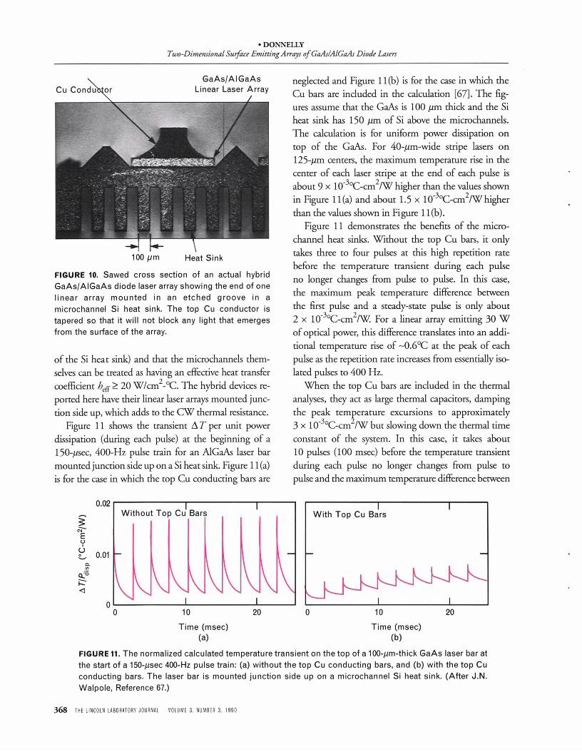
FIGURE 10. Sawed cross section of an actual hybridGaAs{AIGaAs diode laser array showing the end of onelinear array mounted in an etched groove in amicrochannel Si heat sink. The top Cu conductor istapered so that it will not block any light that emergesfrom the surface of the array.
of the Si heat sink) and that the microchannels themselves can be treated as having an effective heat transfercoefficient heff "2. 20 W/cm2
_0C. The hybrid devices reported here have their linear laser arrays mounted junction side up, which adds to the CW thermal resistance.
Figure 11 shows the transient ~T per unit powerdissipation (during each pulse) at the beginning of a150-,usec, 400-Hz pulse train for an AlGaAs laser barmounted junction side up on a Si heat sink. Figure 11 (a)is for the case in which the top Cu conducting bars are
100 Jim Heat Sink
neglected and Figure 11 (b) is for the case in which theCu bars are included in the calculation [67]. The figures assume that the GaAs is 100 ,urn thick and the Siheat sink has 150 ,urn of Si above the microchannels.The calculation is for uniform power dissipation ontop of the GaAs. For 40-,um-wide stripe lasers on125-,urn centers, the maximum temperature rise in thecenter of each laser stripe at the end of each pulse isabout 9 x 1O-3°C-cm2/W higher than the values shownin Figure 11 (a) and about 1.5 x 1O-3°C-cm2/W higherthan the values shown in Figure 11(b).
Figure 11 demonstrates the benefits of the microchannel heat sinks. Without the top Cu bars, it onlytakes three to four pulses at this high repetition ratebefore the temperature transient during each pulseno longer changes from pulse to pulse. In this case,the maximum peak temperature difference betweenthe first pulse and a steady-state pulse is only about2 x 1O-3°C_cm2/W For a linear array emitting 30 W
of optical power, this difference translates into an additional temperature rise of -0.6°C at the peak of eachpulse as the repetition rate increases from essentially isolated pulses to 400 Hz.
When the top Cu bars are included in the thermalanalyses, they act as large thermal capacitors, dampingthe peak temperature excursions to approximately3 x 1O-3°C_cm2/W but slowing down the thermal time
constant of the system. In this case, it takes about10 pulses (100 msec) before the temperature transientduring each pulse no longer changes from pulse topulse and the maximum temperature difference between
0.02
~r;;-Eu,u
0.01L-a.VI
0.."i=:'<l
Without Top Cu Bars
10
Time (msec)(a)
20 o
With Top Cu Bars
10
Time (msec)(b)
20
FIGURE 11. The normalized calculated temperature transient on the top of a 1OO-,um-thick GaAs laser bar atthe start of a 150-,usec 400-Hz pulse train: (a) without the top Cu conducting bars, and (b) with the top Cuconducting bars. The laser bar is mounted junction side up on a microchannel Si heat sink. (After J.N.
Walpole, Reference 67.)
368 THE LINCOLN LABORATORY JOURNAL VOLUME 3. NUMBER 3. 1990

• DONNELLYTwo-Dimensional Surftce Emitting Arrays ofGaAs/AIGaAs Diode Lasers
(a)
(b)
I" -I I" -I1 cm 1 cm
FIGURE 12. Completed module that contains two 1-cm2 two-dimensional surface-emitting arrays of diodelasers: (a) overall view and (b) view of front face.
the peak of a first pulse and the peak of a steady-statepulse is -4.5 x 1O-3°C_cm2/W For a I-em linear laser
array emitting 30 W of optical power, this differencetranslates into an additional temperature rise of-I.38°Cas the repetition rate increases from essentially isolatedpulses to 400 Hz. Note, however, that the transient temperature during each pulse is now only -1.3°C for the30-W scenario compared to -7°C without the top Cubars (Figure 8).
For uniform heat dissipation across the laser bar, theaverage temperature rise is the same both with and
without the Cu bars. For CWoperation, the only effect
of the top Cu bars is to act as heat spreaders, a secondarybut important consideration that makes the temperature across the top ofthe laser bar more uniform and less
dependent on the laser width Wand spacing S.
Hybrid-Array Performance
Figure 12 shows photographs ofa completed laser module that contains two I-em2 hybrid arrays, each ofwhichconsists of eight I-em-long linear arrays soldered ineight grooves on a microchannel Si heat sink. In thisdesign, the linear arrays are driven in pairs. Coolingfluid enters the module through a center tube and
VOLUME 3, NUMBER 3, 1990 THE LINCOLN LABORATORY JOURNAL 369

-DONNELLYTwo-Dimensional Suiface Emitting Arrays ofGaAs/AIGaAs Diode Lasers
FIGURE 13. Near-field pattern of a module that contains two 1-cm2 surface-emitting hybrid AIGaAs GRIN-SCHSQW diode laser arrays.
exits through two outside tubes.Figure 13 shows the near-field pattern ofa completed
module. The geometry of these hybrid arrays is suchthat the amount of thermal cross talk between the individual linear arrays is insignificant. Thus testing the
linear-array bars individually or in pairs one pair at a
Side 1 of Module60
Q; 403:o
c...~
a.:; 20o
o i-=':J....J,~....I.=~~'l-.l.......::~'r-l-=:::I.-...L---L---L---l----J
o 10 0 10 0 10 0 10 20 30 40 50 60
Current (A)
time provides a good idea of the ultimate performance
of the hybrid arrays.Figure 14 shows the output power versus current
(L-I characteristic) of successive pairs of laser bars in a
module driven with 150-.usec current pulses at 10 Hz.Note that the response is very uniform with high T)d
Side 2 of Module
o 10 0 10 0 10 0 10 20 30 40 50 60
Current (A)
FIGURE 14. Pulsed output power versus current for 150-,usec pulses at 10 Hz into successive pairs of laser bars of amodule that contains two 1-cm2 two-dimensional surface-emitting hybrid arrays of AIGaAs diode lasers.
370 THE LINCOLN LABORATORY JOURNAL VOLUME 3. NUMBER 3. 1990

• DONNELLYTwo-DimensionalSuiface Emitting Arrays ofGaAslAIGaAs Diode Lasers
Wavelength (nm)
815810805
.0 L...-__~~L-__~_L- ----I
800
80 A~
1.0c
::::>~
~~
-e~ 0.5:;.&::J
0
for all pairs in the array. From these data, the totalenergy per 150-,usec pulse from the entire modulewith 60 A through each pair (30 A per I-em-longlinear array) should be 68 m]. Separate measurements using a calorimeter with the entire moduledriven at one time have given a total energy of 64 m]per pulse [68].
Figure 15 shows the L-I characteristics of a pair oflaser bars driven with 150-f.1Sec pulsed currents up to
100 A. From these data, we estimate that if the entiremodule were driven with 100 A per pair (50 A perbar), the output energy per pulse would be -120 mJ.Figure 16 shows the integrated output spectra of the
Two 1-cm Bars in Parallel100
~80
~
"-Ql
~ 600
Cl.....::J0- 40....::J
0
20
00 20 40 60
Current (A)
80 100
FIGURE 16. Output spectra of a pair of paralleI1-cm-longbars of GRIN-SCH-SQW lasers (40,um wide on 125-,umcenters) of a hybrid array. The bars were driven with40-A (20 A/bar) and 80-A (40 A/bar) 150-llsec pulses at10 Hz.
driven with 150-f.1Sec pulses at various currents up to
30 A at 10 Hz, and with 150-,usec pulses of 30 A atrepetition rates from 10 to 500 Hz. At the higher currents, the output of the particular bar tested showedanomalous blue-shifted modes, which are not usuallyobserved. The wavelength change at 30 A comparedwith that at 7 A indicated a temperature rise of <3°Cduring a 30-A 150-f.1Sec pulse. (As mentioned previously, the wavelength ofAlGaAs lasers increases by -0.3 nm
FIGURE 15. Pulsed output power versus current of asingle pair of parallel 1-cm laser bars of a hybrid arraydriven with 150-,usec pulses at 10 Hz. One 1-cm Bar
40
laser pair driven with 40-A (20 A/bar) and 80-A
(40 A/bar) 150-f.1Sec pulses at 10Hz. The spectra aretypical ofmost arrays.
Additional tests were performed by disconnectingone bar of several pairs and then testing the remainingbars individually at various currents, pulse widths, andrepetition rates. Figure 17 shows the L-I characteristics
of one I-em-long bar of a hybrid array driven with150-f.1Sec pulses at repetition rates up to 500 Hz. The lasers in the array were 40 ,urn wide and spaced on centerat 125 pm. Note that at 40 A, there was less than
a 10% decrease in output per pulse at 500 Hz compared with that at 10 Hz.
We also obtained the output spectra of the same bar
~~
"-30Ql
~0
Cl.....20::J
0-....::J
0
FIGURE 17. Pulsed output power versus current of one1-cm-long GRIN-SCH-SQW laser bar of a hybrid twodimensional surface-emitting array driven with 150-psecpulses at repetition rates up to 500 Hz. The AIGaAsdiode lasers were 40,um wide on 125-,um centers.
VOLUME 3. NUMBER 3. 1990 THE LINCOLN LABORATORY JOURNAL 371

-DONNELLYTwo-Dimensional Surfizce Emitting Arrays ofGaAs/AlGaAs Diode Lasers
50 .--....----,.-..--....----,.-..--....-----r-..---,-----r---,
Wavelength (nm)
FIGURE 18. Output spectra of one 1-cm-long GRINSCH-SQW laser bar of a hybrid two-dimensional surface-emitting array driven with 30-A 150-.usec pulses atrepetition rates of 10, 100,400, and 500 Hz. The AIGaAsdiode lasers were 40 jim wide on 125-.um centers.
per 1°C rise in temperature.) Figure 18 shows the out
put spectra of the bar driven with 150-jisec pulses of
30 A at repetition rates of 10, 100, 400, and 500 Hz.
The additional temperature rise at the high repetition
rates appears to be less than 1°C.
Figure 19 shows the L-I characteristics ofa single bar
for pulses ranging from 150 jisec to 1 msec at 10Hz.
The figure also shows the CW output for currents up to
25 A. Figure 20 contains a blow-up of the CW charac-
One 1-cm Bar 0.9 >.u
3' 20 cQl
0.7 u~ :;::.... ...-Ql 15 w~ ....0 0.5 Ql
a.. ~..... 10 0:J a..c...... 0.3:J ~0 5 Ql
>
0.1 0
00 5 10 15 20 25 30
Current (A)
teristics and the overall power efficiency TJp versus cur
rent. Note that the overall CW TIp at 25 A (including
losses in the input wires that were not intended for CW
operation) is 33%. For 150-jisec pulses, TJp (again in
cluding losses in the input wires) is -38% at 40 A. We
also measured the output spectra for 8-A 150-jisec
pulses at 10 Hz and for 7- and 25-A CWoperation.
From that data, the estimated temperature rise for
25-A CW operation was -30°C.
We can use this value of temperature rise and an
estimate of the power dissipated in the laser bar itself to
obtain an estimate of the thermal resistance of the laser-
FIGURE 20. The CW output power and overall powerefficiency versus current of one 1-cm-long GRIN-SCHSQW laser bar of a hybrid two-dimensional surfaceemitting array. The AIGaAs diode lasers were 40.um wideon 125-.um centers.
25 r--,..----r-----r--..---....----,
815810
10 Hz
" I
___ 500 Hz__ 400 Hz
I
805
J
100 HZ--:~
1 '/
a
I
800795
One 1-cm Bar40
3'~
....30Ql
~0
a.......
20:JC......:J
010
o L....£--'---(f-L....&-.L-ff-l-~-{f-J...."L...L..j.f--L..L....L...---L.---L---'
o 10 0 10 0 10 0 10 0 10 20 30
Current (A)
FIGURE 19. Output power versus current of one 1-cmlong GRIN-SCH-SQW laser bar of a hybrid two-dimensional surface-emitting array driven with 150-, 300-, and600-.usec and 1-msec pulses at 10 Hz. Also shown is theCW output for current up to 25 A. The AIGaAs diodelasers were 40.um wide on 125-.um centers.
bar/heat-sink combination. For 25-W CW operation,
the total power into the laser bar (assuming each of the
80 lasers in the 1-cm bar has a series resistance of0.2 Q)is -40 W Thus, with an optical power output of 18 W,the dissipated power in the laser bar is -22 W With this
dissipated power, the CW temperature rise of-30°C gives
a total effective thermal resistance of -0.094°C-cm2/WThis result is in close agreement with previous heat-sink
measurements and calculations: from References 58 and
60, the thermal resistance is -0.07°C-cm2/W for the Si
heat sink and -0.02°C-cm2/W for the 100-jim-thick
laser bar.
After operating a bar in CW mode at 25 A for about
15 min, we measured the L-I characteristic of the bar
driven with 150-jisec pulses at 10Hz. The results indi
cated insignificant degradation «5%) after the CW
testing [50J.
372 THE LINCOLN LABORATORY JOURNAL VOLUME 3. NUMBER 3. 1990

-DONNELLYTwo-Dimensional Surface Emitting A"ays ofGaAs/AIGaAs Diode Lasers
100
0.75-cm 2 Array Area
~80
~
'-<ll~ 600
a.....-::Ja.
40...-::J
0
~u 20
00 30 60 90 120 150 180
Drive Current (A)
intracavity 45° deflecting mirrors have been fabricated
(Figures 22[b] and [c]) [21,23]. In both types ofarrays,
ion-bearn-assisted etching (IBAE) was used to form all
the laser facets and deflecting mirrors.
FIGURE 21. CW output power versus current of six
1-cm-long linear arrays (0.75-cm2 area) of a hybrid
microchannel-cooled module operated in parallel.
Monolithic Surface-Emitting Diode Laser Arrays
Although hybrid arrays have excellent performance
characteristics, the fabrication and assembly of this type
of laser require a great deal ofskilled labor. Researchers
are hopeful that monolithic arrays, which can be fabri
cated almost entirely with high-volume semiconductor
processing techniques, will be more arnenable to mass
production. As a possible direct replacement for hybrid
arrays, monolithic two-dimensional arrays of GaAs/
AlGaAs diode lasers with light emission normal to the
surface have been made by fabricating horiwntal-cavity
edge-emitting quantum-well lasers coupled with exter
nal mirrors that deflect the radiation from the laser
facets by 90° (Figure 22 [a]) [21,23,37,38]. In addition,
several preliminary surface-emitting arrays with
Figure 21 shows the CW output power versus cur
rent of six bars (0.75 cm2) operating in parallel. Note
that at 25 A per bar (a total current of 150 A), the
output power is 90 W, or 120 W/cm2, which is slightly
less than the 144 W/cm2 (18 W/bar x 8 bars/cm2) ob
tained from the single-bar data ofFigure 20.
(a)
(b)
(c) TDielectric Stack
FIGURE 22. Geometries of three designs of monolithic sur
face-emitting lasers: (a) external-cavity parabolic deflector,
(b) intracavity 45° mirror, and (c) intracavity 45° mirror withan internal dielectric mirror stack.
VOLUME 3. NUMBER 3, 1990 THE LINCOLN LABORATORY JOURNAL 373

-DONNELLYTwo-Dimensional Surface Emitting Arrays ofGaAs/AIGaAs Diode Lasers
Argon Gas
~
.....-H+--++- Tungsten Filament
Carbon GridsA node ---tl---*I
Argon-IonFlux 500eV ---I-I--~:itt7t7- "'I--~r- Neutralizer
Masked Substrate ---tl--
on Sample Stage
Gate Valve
Substrate Holder -----./
...--- Load Lock
~§~---I"~Rough Vacuum
FIGURE 23. Schematic of CI2-ion-beam-assisted-etching (IBAE) system.
IBAE is a dry-etching technique in which the chemi
cally reactant species and the energetic ions can beindependently controlled. In Reference 42, Geis et al.
describe the basic IBAE system. Figure 23 is a schematic
illustration of an IBAE system with load lock, tiltable
sample holder, and cryopump. In the system, which
routinely reaches a background pressure of 10-7 Torr
15 min after sample loading, a chemically reactant spe
cies from a local jet and a separately controlled collimated
ion beam from an ion source impinge simultaneously
upon the sample. Both GaAs and AlGaAs can be etched
at room temperature with Cl2 as the reactant gas and
argon as the source of ions. Because neither GaAs nor
AlGaAs is spontaneously etched by Cl2 at room tem
perature, IBAE is higWy directional and the sidewall
slope of a masked etch trench is determined essentially
by the direction ofthe argon-ion beam. Therefore, almost
any concave shape can be generated with a computer
controlled sample stage that precisely varies the tilt anglebetween the sample and the ion beam during etching
[44]. Materials such as photoresist, phosphosilicate glass,
Si02, Ni, and Ti that have slow etch rates compared to
GaAs and AlGaAs can be used as etch masks.
For the work reported in this article, the system
operating parameters were adjusted to give an etch rate
of 120 nm/min at normal incidence for both GaAs and
AlGaAs. The energy of the argon-ion beam was 500 eVand the current density was -40 mNcm2
. The pressure
due to the argon-ion beam at the sample surface was
0.1 mTorr and the local chlorine pressure was2.8 mTorr. With these parameters, we observed no
roughness or steps at the GaAs/AlGaAs heterointerfaces.
Monolithic Arrays with External DeflectingMirrors
We have fabricated monolithic two-dimensional sur
face-emitting arrays of GaAs diode lasers by using a
combination of straight and angled IBAE to produce
arrays ofedge-emitting separate-confinement quantum
well lasers with deflecting mirrors adjacent to the laser
facets (Figure 24). The AlGaAs/GaAs material used for
these arrays was separate-confInement-heterostructure
single-quantum-well (SCH-SQW) material that con-
374 THE LINCOLN LABORATORY JOURNAL VOLUME 3, NUMBER 3. 1990

-DONNELLYTwo-Dimensional Suiface Emitting Arrays ofGaAslAIGaAs Diode Lasers
DeepProton-Bombarded
Region
- - - -}- - --
ActiveLayer
ShallowProton-Defined
Laser Stripe
"'EtchedLaser Facets
-I -Sf.Jm tNi/Ge/Au
Back Contact
FIGURE 24. Schematic illustration of a monolithic two-dimensional surface-emitting array of GaAs/AIGaAs diode lasers with external parabolic deflecting mirrors.
tained an undoped 200-A GaAs quantum well sand
wiched between twO 3200-A-thick Alo.3Gao.7As confining layers, one n-type and the other p-type. The
cladding layers contained 70 mole % AlAs. Cleavedfacet lasers fabricated from this SCH-SQW material
had higher threshold current densities and lower differ
ential quantum efficiencies (TId == 60%) than those oftheGRIN-SCH-SQW material (Figure 3) now being used
for the hybrid arrays. Because ofthe wide quantum-well
thickness of the monolithic array lasers, however, the
threshold current density does not increase as rapidly
with decreasing cavity length. Nevertheless, longer cav
ity lengths than those used in the arrays reported in thisarticle should result in better performance.
We used photoresist as an etch mask and IBAE to
etch pairs of straight-sided grooves 2 pm wide and 3 to
4 pm deep. The outer walls of each pair acted as the
facets for rows of laser cavities that were 250 pm long.
Lines approximately 3 pm wide immediately adjacent
to the inside edge ofone ofthe grooves in each pair were
then opened in a new layer ofphotoresist, and parabolic
deflectors for one side of each row were formed by
computer-controlled angled IBAE. The deflectors for
the other side of each row were formed in a similar
manner.
Figure 25 shows the near-field pattern of a
100-element two-dimensional surface-emitting array. Ashallow proton bombardment was used to confine the
current to 40-pm-wide stripes on lBO-pm centers, and
a deep proton bombardment midway between the laser
stripes was used to introduce a sufficient optical loss to
suppress transverse lasing. References 21 and 36 con
tain further details of the fabrication. Figure 26 plots
the pulsed output power versus current for this array.
The available pulsed current of62 A limits the power to
15 W Figure 27 plots the output power versus cur
rent for an array that consists of only two rows (a
total of 20 elements) fabricated from the same wafer
as that of Figure 26. The smaller array has a pulsed
• • • • • • • • • • •• • • • • • • • • • •• • • • • • • • • • •• • • • • • • • • • •• • • • • • • • • • •• • • • • • • • • • •• • • • • • • • • • •• • • • • • • • • • •• • • • • • • • • • •• • • • • • • • • • •
FIGURE 25. Near-field pattern of 100-element monolithictwo-dimensional surface-emitting array of GaAs/AIGaAsdiode lasers with external deflecting mirrors.
VOLUME 3, NUMBER 3, 1990 THE LINCOLN LABORATORY JOURNAL 375

-DONNELLYTwo-Dimensional Suiface Emitting Arrays ofGaAslAIGaAs Diode Lasers
70605040302010
16
14
~ 12~
....Q)
:;: 100
a......::J 8a.....::J
06
4
2
mentioned previously, cleaved-facet lasers fabricated inthe GRIN-SCH-SQW material also have a higher dif
ferential quantum efficiency [>80%].) In addition,making the junction slightly deeper (2.5 to 3 J..Lffi deepinstead of 2 J..Lffi) and the facet etch narrower (l to 1.5J..Lffi wide instead of2 f.1m) should increase the collectionefficiency of the deflecting mirrors and make them moretolerant of photolithographic and etching inaccuracies.
With a planar top surface, curved deflectors are necessary to obtain an f-number less than 1. Figure 28shows a design ofan integral parabolic deflecting mirrorwith an f-number less than 0.85. The actual curve
etched in the AlGaAs material is now being designed tooptimize the f-number, with attention to the following
factors: passivation and metal overlayers, the depth ofthe junction, and tolerances in the lithography used to
form the etch mask. For the front surface of the deflec
tor to be parabolic, etching a second-order polynomialcurve IS necessary.
Figure 29(a) illustrates the method [23] that we arenow using to etch the curve in the laser material. First
the curve is broken down into a number of line seg-
Pulsed Current (A)
FIGURE 27. Pulsed output power versus current for a 20element (two rows of 10 elements) two-dimensionalarray of GaAs{AIGaAs diode lasers. The pulses are500 nsec at 1 kHz and the array area is 1.08 x 10⁻² cm2
.
18 .----.,....---r----,--~-___,--r_____,
70605040302010
OL.o::::;_....L..._.......L.._--1__..L.-_...J...._--'-_---'
o
18
16
14
12
~....
10Q)
:;:0
a...... 8::Ja.....::J
06
4
2
power output of 16.5 W at 62 A, which corresponds to
a power density of 1.5 kW/cm2 [21,23,37,38].
The differential quantum efficiency 1')d of these arrays
is about 20%. Several factors can limit 1')d, including the
quality of the laser facets, the beam divergence of the
laser emission, and the effective f-number of the deflect
ing mirrors. The latter two factors affect the fraction of
light emitted from the laser facets that is deflected by the
deflecting mirrors. Although the quality of the laser
facets can be a problem, the fraction deflected by the
mirrors is currently the major limitation on 1')d.
We can make several obvious changes to increase the
fraction of light collected and to make this fraction less
dependent on process variables. The first is to use laser
material with a smaller output-beam divergence. Cleaved
facet lasers fabricated in the GRIN-SCH-SQW materi
al now being used in the hybrid arrays have a beamdivergence ~36° (full width at halfmaximum), which is
significantly smaller than the ~45° measured in similarlasers fabricated in the SCH-SQW material used for the
array whose near-field pattern is shown in Figure 25. (As
Pulsed Current (A)
FIGURE 26. Pulsed output power versus current for the100-element monolithic array whose near-field pattern isshown in Figure 25. The pulses are 500 nsec at 1 kHzand the area of the array is 5.4 x 10⁻² cm2
.
376 THE LINCOLN LABORATORY JOURNAL VOLUME 3. NUMBER 3. 1990

-DONNELLYTwo-Dimensional Surface Emitting Arrays ojGaAs/AIGaAs Diode Lasers
.JIlrolI1---:"-' Final MetallizedParabolic Reflector
~I-- Etched Reflector
2.5 Jim
GaAs ~Quantum - .....-01
Well .................... e............
........
1.....11------ 4.5 Jim------J~--
----.,....-i
FIGURE 28. Illustration of an external deflecting mirror. The effective f-number is less than 0.85and the minimum e is 30.5°.
ments of length Ln, which is determined by the resolution of the computer-controlled stepping motor. Oncethe daily etch rate is determined, the time requiredto etch each segment tn is calculated from the formula
tn = L)(r cos cfJ), where r is the etch rate and cfJn is theincident angle of the argon-ion beam. The resolution
of the steps coupled with the slight divergence of theion beam (-0.5°) create a smooth surface with
the individual etched segments blended together.Figure 29(b) compares the desired theoretical curvewith an actual etched curve. Note the excellent agreement berween the rwo curves; the small amount ofdeviation is most likely due to an error in determiningthe etch rate. To achieve even greater accuracy, we arecurrently determining the rate by using a surface
profIle technique in place ofoptical microscopy.The scanning-electron micrographs in Figure 30 show
the face of a typical etched facet and the surface of atypical etched deflector. We found that a photoresistmask did not hold up well during the vertical-facetformation but was sufficient for etching the deflectors
because the tilting action in the latter procedure shiftedthe edge of the mask and minimized the mask-edge
erosion. We are now using a silicon-dioxide mask foretching and a self-aligning process for accurately fIxingthe facet-to-deflector distance. With these changes, it
should be possible to fabricate parabolic deflecting mirrors with effective f-numbers less than one and arrays
with l1d > 60%.
Monolithic Arrays with Intracavity Deflecting Mirrors
Using a combination ofstraight and 45° IBAE, we havefabricated monolithic rwo-dimensional surface-emittingarrays with intracavity 45° mirrors (Figure 31) [21, 23].Lasers of this type are sometimes called folded-cavitylasers [22, 23]. We etched the arrays in one photolithog
raphy step. With photoresist as an etch mask, we usedIBAE to etch straight-sided grooves 6 pm wide. Without removing the sample from the etch chamber, wetilted the sample at a 45° angle and etched the 45°intracavity mirrors. Figure 32, an optical micrograph ofa cleaved cross section ofan IBAE test sample, shows thesuccess of the technique. Some erosion of the photoresist etch mask occurred, which produced steps in thevertical facet and 45° mirror. The step in the verticalfacet, however, was above the laser active layer and the
VOLUME 3. NUMBER 3, 1990 THE LINCOLN LABORATORY JOURNAL 377

• DONNELLYTwo-Dimensional Suiface Emitting Arrays ofGaAslAIGaAs Diode Lasers
1 Jim(b)
I~
1....-- 10 Jim---+-I(a)
efficiency is low, about 4%. One factor that degraded
the performance of this first array was the optical loss in
the p+-GaAs capping layer, which was not removed
from the window region.
Obviously, more work is needed to improve the qual
ity and accuracy of both the 45° etch and the verticaletch in this device. Other parameters that could poten
tially limit the performance of the device are the parallel
ism and quality of the top surface facet, the diffraction
between the top facet and the 45° mirror, and the
absorption in any GaAs contacting layer left on the
surface of the wafer. We expect the use of a silicon-
FIGURE 30. Scanning-electron micrographs of (a) the
face of an etched vertical facet and (b) the etched
surface of a parabolic deflector.
Ih"-- Line Segmentsn-~ Programmed
into Etcher~~_~~~...-- Curve
to Be Etched
(a)
FIGURE 29. (a) Dynamic tilting algorithm employed in
micromachining the polynomial curve required to pro
duce a parabolic deflector. The quantity tln is the angu
lar displacement generated by a step of the motor, andLn is the segment length at each step. (b) Optical
micrograph of a cleaved cross section of a parabolicdeflector. The black curved line represents the desired
theoretical curve.
step in the 45° mirror was below the active layer. Thus
their effect on device performance was not catastrophic.
Figure 33 shows the near-field pattern of a
100-element array. Note the one bad element in the
fourth row and the scattering in the fifth row. All of the
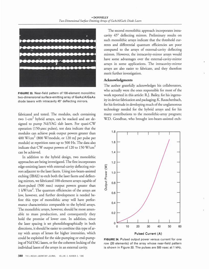
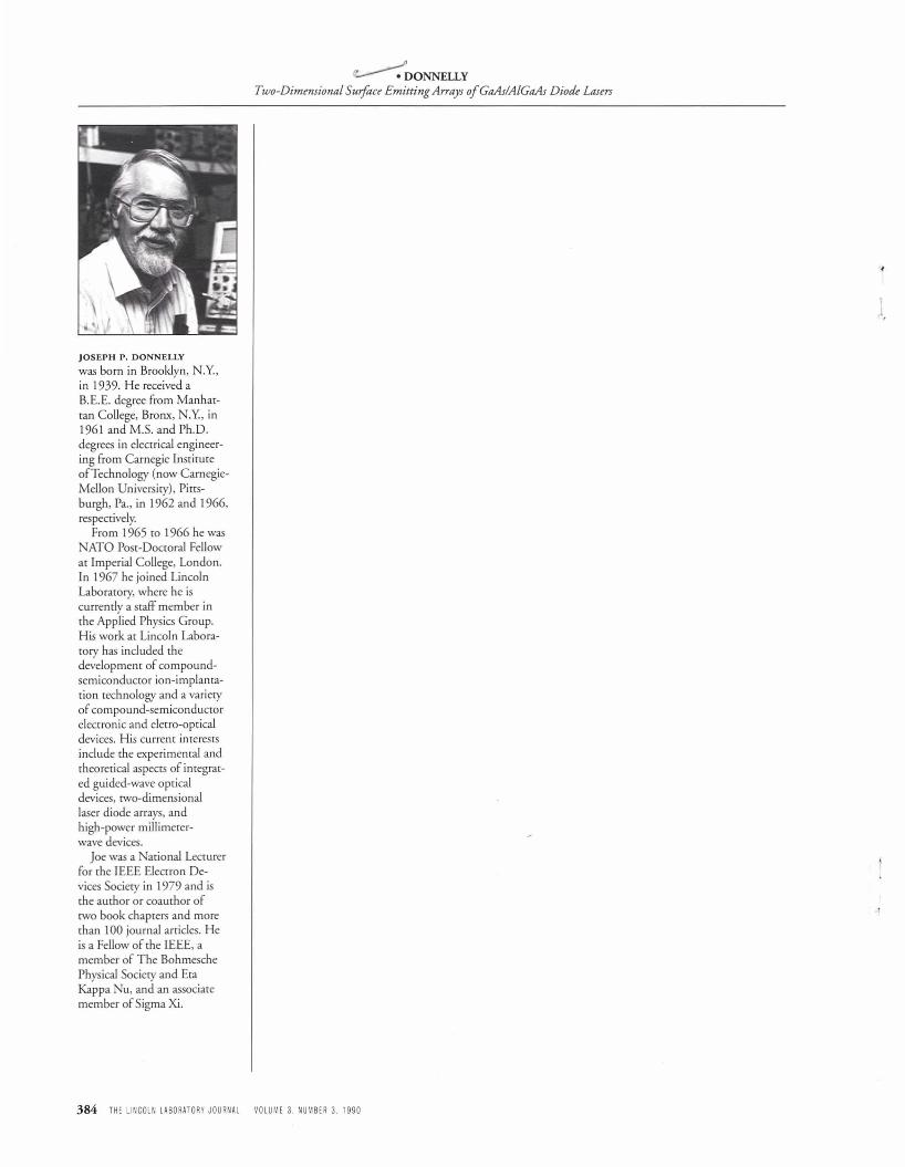
other lasers were operational. Figure 34 shows the pulsed
output power versus current for the first row ofthe array
(a total of20 elements). The average threshold current is
high, about 1 A per laser, and the differential quantum
378 THE LINCOLN LABORATORY JOURNAL VOLUME 3, NUMBER 3, 1990

• DONNELLYTwo-Dimensional Surface Emitting Arrays ofGaAs/AIGaAs Diode Lasers
DeepProton-Bombarded
Region
Etched45° Intracavity
Mirror
Cr/AuMetallization
ActiveLayer
WindowRegion
EtchedLaser Facet
ShallowProton-Defi ned
Laser Stripe
Ni/Ge/AuBack Contact
FIGURE 31. Schematic illustration of a monolithic two-dimensional surface-emitting array of GaAs/AIGaAs diode lasers with intracavity 45° deflecting mirrors.
dioxide or metal etch mask to improve the quality of the
surfaces dramatically, which would in turn improve
array performance. In addition, future arrays will be
fabricated with the capping layer removed.
We have also fabricated monolithic arrays that had
two internal 45° mirrors and an integral high-reflectivity
dielectric mirror stack (Figure 22[c]) [23]. For this type
of array, forming the internal and top-surface facets in
one step minimized the IBAE and processing time. The
dielectric mirror stack, which consisted of 20 pairs of
alternating layers ofAlQ.2Gao.sAs and Alo.sGao.~, hada reflectivity of -95% at the lasing wavelength of inter
est. The arrays performed similarly to the internal-cavity45° mirror arrays that had one etched 90° facet.
In addition to the problems associated with arrays
that have one etched 90° facet, diffraction and series
resistance in the dielectric mirror stack must be consid
ered for the arrays that have two internal 45° mirrors. Asdiscussed earlier, berrer-quality 45° mirrors and the re
moval of the p+-GaAs capping layer should improve the
performance of this type of laser.
Summary
Several approaches to fabricating two-dimensional sur
face-emitting arrays of GaAs/AlGaAs diode lasers are
being developed at Lincoln Laboratory.
Modules of hybrid diode laser arrays that utilize lin
ear laser arrays with cleaved facets and microchannel Si
heat sinks with integral 45° deflecting mirrors have been
FIGURE 32. Optical micrograph of the cleaved crosssection of a test wafer, profiling the vertical facet and45°-mirror structure of the intracavity 45° deflecting mirror, or folded-cavity, design. After the vertical facet isformed, the sample is tilted in situ and the 45° mirror isetched.
VOLUME 3. NUMBER 3. 1990 THE LINCOLN LABORATORY JOURNAL 379
-DONNELLYTwo-Dimensional Suiface Emitting Arrays ofGaAs/AIGaAs Diode Lasers
FIGURE 33. Near-field pattern of 100-element monolithictwo-dimensional surface-emitting array of GaAs/AIGaAsdiode lasers with intracavity 45° deflecting mirrors.
fabricated and tested. The modules, each containing
two l-cm2 hybrid arrays, can be stacked and are de
signed to pump Nd:YAG slab lasers. For quasi-CW
operation (150-psec pulses), test data indicate that the
modules can achieve peak output powers greater than
400 W/cm2 (800 W/module, or 120 m] per pulse per
module) at repetition rates up to 500 Hz. The data also
indicate that CW output powers of 120 to 150 W /cm2
can be achieved.
In addition to the hybrid design, two monolithic
approaches are being investigated. The first incorporates
edge-emitting lasers with external-cavity deflecting mir
rors adjacent to the laser facets. Using ion-bearn-assisted
etching (IBAE) to etch both the laser facets and deflect
ing mirrors, we fabricated 1OO-element arrays capable of
short-pulsed (500 nsec) output powers greater than
1 kW/cm2. The quantum efficiencies of the arrays are
low, however, and further development is needed be
fore this type of monolithic array will have perfor
mance characteristics comparable to the hybrid arrays.
The monolithic arrays, however, should be more arnen
able to mass production, and consequently they
hold the promise of lower cost. In addition, since
the laser spacing is set photolithographically in both
directions, it should be easier to combine this type ofar
ray with arrays of lenses for higher intensities, which
could be exploited for the side-pumping or end-pumping of Nd:YAG lasers, or for the coherent locking ofthe
individual lasers of the arrays in an external cavity.
380 THE LINCOLN LABORATORY JOURNAL VOLUME 3. NUMBER 3. 1990
The second monolithic approach incorporates intra
cavity 45° deflecting mirrors. Preliminary results on
such monolithic arrays indicate that the threshold cur
rents and differential quantum efficiencies are poor
compared to the arrays of external-cavity deflecting
mirrors. However, the intracavity-mirror arrays would
have some advantages over the external-cavity-mirror
arrays in some applications. The intracavity-mirror
arrays are also easier to fabricate, and they therefore
merit further investigation.
Acknowledgments
The author gratefully acknowledges his collaborators,
who actually were the ones responsible for most of the
work reponed in this article: R.]. Bailey, for his ingenu
ity in device fabrication and packaging; K. Rauschenbach,
for his fortitude in developing much ofthe unglarnorous
technology needed for the hybrid arrays and for his
many contributions to the monolithic-array prograrn;
WD. Goodhue, who brought ion-bearn-assisted etch-
1.8
1.6
1.4
1.2
~....
1.0Ql
~0
a......0.8::J
a.....::J
00.6
0.4
0.2
00 10 20 30 40 50 60
Pulsed Current (A)
FIGURE 34. Pulsed output power versus current for onerow (20 elements) of the array whose near-field patternis shown in Figure 33. The pulses are 500 nsec at 1 kHz.

• DONNELLYTwo-Dimensional Surface Emitting Arrays ofGaAs/AIGaAs Diode Lasers
ing to the fabrication ofmonolithic arrays; CA. Wang,for her unique talent and perseverance in developing the
epitaxial technology necessary to grow the high-qualitylaser material used in this work and for not quittingwhen she was told the program needed "only" 40 morewafers; J.N. Walpole, for his insights into semiconductor diode lasers and microchannel heat sinks and forhis numerical heat-flow calculations; L.J. Missaggia, forhis many contributions to this program, especially hisexpertise in heat-sink-module design and assembly;J.D. Woodhouse, for supervising the fabrication of thelinear arrays; V. Diadiuk, for her unselfish effort in producing the microchannel Si heat sinks; and V. Daneu,
for his independent measurements on the hybrid arrays. The author would also like to acknowledge H.K.Choi, EJ. O'Donnell, GA. Ferrante, G.D. Johnson,D.B. Hoyt, and CD. Hoyt for their many contribu
tions to this project, and S.M. McNeill, P.S. Day,M.D. McAleese, and D.M. Tracy for their technicalassistance. The continued interest of R.C Williamson,D.L. Spears, A. Sanchez-Rubio, and 1. Melngailis is
also greatly appreciated.This work was sponsored by the Department of the
Navy for SDIO and the Department of the Air Force.
REFERENCES
1. G.L. Harnagel, P.S. Cross, e.R. Lennon, M. Devito, andD.R. Scifres, "Ultra-High-Power Quasi-CW Monolithic Laser Diode Array wirh High Power Conversion Efficiency,"Electron. Lett. 23, 743 (1987).
2. D.F. Welch, W. Streifer, B. Chan, and D.R. Scifres, "HighPower, 8 W CW, Single-Quamum-Well Laser Diode Arrays," Electron. Lett. 24, 113 (1988).
3. M. Sakamoto, D.F. Welch, G.L. Harnagel, W. Streifer, H.Kung, and D.R. Scifres, "Ultra-High-Power 38 W Continuous-Wave Monolithic Laser Diode Arrays," Appl Phys. Lett.52, 2220 (1988).
4. M. Sakamoto, D.F. Welch, TG. Erdriz, D.R. Scifres, and W.Streifer, "76 W CW Monolithic Laser Diode Arrays," ApplPhys. Lett. 54, 2299 (1989).
5. L.]. Mawst, D. Borez, M.Jansen, TJ. Roth, and G. Pererson,"High-Power, Narrow Single-Lobe Operation from 20-Element Phase-Locked Array ofAntiguides," Appl Phys. Lett. 55,2060 (1989).
6. M. Jansen, J.J. Yang, S.S. Ou, D. Botez, J. Wilcox, and L.Mawst, "Diffraction-Limited Operation from MonolithicallyIntegrated Diode Laser Array and Self-Imaging (Talbot) Caviry," Appl Phys. Lett. 55, 1949 (1989).
7. P.S. Cross, G.L. Harnagel, W. Streifer, D.R. Scifres, and D.F.Welch, "Ultrahigh-Power Semiconductor Diode Laser Arrays," Science237, 1305 (1987).
8. W. Streifer, D.R. Scifres, G.L. Harnagel, D.F. Welch, ].Berger, and M. Sakamoto, "Advances in Diode Laser Pumps,"IEEE] Quantum Electron. 24, 883 (1988).
9. e.A. Krebs and B.D. Vivian, "High Power Quasi-CW andCW Laser Diode Bar Arrays," SPIE893, 35 (1988).
10. A. Rosenberg,].e. McShea, A.R. Bogdan, J.e. Petheram, A.Rosen, D. Bechtle, P.S. Zory, ].W. Sprague, and J.R. Shealy,"High-Power, High-Efficiency 770 nm 2D Laser Diode Array," Electron. Lett. 24,1121 (1988).
11. A. Rosen, P. Stabile, W. Janton, J.e. McShea, A. Rosenberg,J.e. Petheram, H.G. Miller, ].W. Sprague, andJ.M. Gilman,"1 kw Peak Power 808 nm 2-D Laser Diode Array," IEEEPhotonics Technol Lett. 1,43 (1989).
12. K Iga, F. Kayama, and S. Kinoshita, "Surface Emitting Semiconductor Lasers," IEEE] Quantum Electron. QE-24, 1845(1988).
13. M.Y.A. Raja, S.R.J. Brueck, M. Osinski, e.F. Schaus, ].G.McInerney, TM. Brennan, and B.E. Hammons, "ResonantPeriodic Gain Surface-Emitting Semiconductor Lasers," IEEE] Quantum Electron. 25, 1500 (1989).
14. S.W. Corzine, R.S. Geels, J.W. SCOtt, R.-H. Van, and L.A.Coldren, "Design ofFabry-Perot Surface-Emitting Lasers witha Periodic Gain Structure," IEEE] Quantum. Electron. 25,1513 (1989).
15. L.M. Zinkiewicz, TJ. Roth, L.J. Mawst, D. Tran, and D.Botez, "High Power Vertical-Caviry Surface-Emitting AlGaAs/GaAs Diode Lasers," Appl. Phys. Lett. 54, 1959 (1989).
16. D. Botez, L.M. Zinkiewicz, TJ. Roth, L.]. Mawst, and G.Peterson, "Low-Threshold-Current-Densiry Vertical-CavirySurface-Emitting A1GaAs/GaAs Diode Lasers," IEEE Photonics Technol. Lett. 1,205 (1989).
17. J.L. Jewell, KF. Huang, K. Tai, Y.H. Lee, R.J. Fischer, S.L.McCall, and A.Y. Cho, "Vertical Caviry Single QuantumWell Lasers," Appl. Phys. Lett. 55, 424 (1989).
18. A.J. SpringThorpe, "A Novel Double-Heterostructure p-nJunction Laser," Appl Phys. Lett. 31, 524 (1977).
19. T Yuasa, N. Hamao, M. Sugimoto, N. Takado, M. Ueno,H. Iwata, Y. Tashiro, K Onabe, and K Asakawa, "SurfaceEmitting GaAs/A1GaAs Multi-Quantum Well Lasers withOptical Bistabiliry," Coni Lasers Electro-Optics Tech. Dig. 19887,258 (1988).
20. N. Hamao, M. Sugimoto, N. Takado, Y. Tashiro, H. Iwata,T Yuasa, and K Asakawa, "Surface-Emitting GaAs/AlGaAsLasers with Dry-Etched 45° Total Reflecting Mirrors," Appl.Phys. Lett. 54, 2389 (1989).
21. J.P. Donnelly, K Rauschenbach, e.A. Wang, W.D. Goodhue,and R.J. Bailey, 'Two-Dimensional Surface-Emitting Arraysof GaAs/A1GaAs Diode Lasers," Proc. SPIE 1043, 92 (1989).
22. T Takamori, L.A. Coldren, and J.L. Merz, "Folded-CaviryTransverse Junction Stripe Surface-Emitting Laser," Appl. Phys.Lett. 55, 1053 (1989).
23. W.D. Goodhue, K Rauschenbach, e.A. Wang,].P. Donnelly, R.J. Bailey, and G.D. Johnson, "Monolithic Two-Dimensional GaAs/A1GaAs Laser Arrays Fabricated by ChlorineIon-Beam Assisted Etching,"] Elettron. Mater. 19,463 (1990).
24. S.S. Ou, M. Jansen, J.J. Yang, and M. Sergant, "High Performance GaAs/A1GaAs Edge-Emitting and Surface-EmittingLasers with Reliable Dry Etched Facets," presented as pOStdeadline paper at CLEO '90, Anaheim, CA, CPDP31.
25. Z.L. Liau, J.N. Walpole, L.J. Missaggia, and D.E. Mull,"GaInAsP/InP Buried-Heterostructure Surface Emitting Diode Laser with Monolithic Integrated Bifocal Microlens,"Appl Phys. Lett. 56, 1219 (1990).
26. G.A. Evans, N.W. Carlson, J.M. Hammer, M. Lurie, J.K
VOLUME 3. NUMBER 3. 1990 THE LINCOLN LABORATORY JOURNAL 381

• DONNELLYTwo-Dimensional Surface Emitting Arrays ofGaAs/AIGaAs Diode Lasers
Butler, S.L. Palfrey, R Amantea, L.A Carr, F.Z. Hawrylo,E.A. James, C]. Kaiser, J.B. Kirk, and W.F. Reichert, ''TwoDimensional Coherent Laser Arrays Using Grating SurfaceEmission," IEEE]. Quantum. Electron. 25, 1525 (1989).
27. G.A. Evans, N.W. Carlson, J.M. Hammer, M. Lurie, J.K.Butler, L.A. Carr, F.Z. Hawrylo, E.A. James, CJ. Kaiser, J.B.Kirk, W.F. Reichert, S.R Chinn, J.R Sheahy, and P.S. Zory,"Efficient, High-Power (>150 mW) Grating Surface Emitting Lasers" App! Phys. Lett. 52, 1037 (1988).
28. J.S. Mott and S.H. Macomber, ''Two-Dimensional SurfaceEmitting Distributed Feedback Laser Arrays," IEEE PhotonicsTechno! Lett. 1,202 (1989).
29. R Parke, R Waares, D.F. Welch, A. Hardy, and W. Streifer,"High Efficiency, High Uniformity Grating Coupled Surface-Emitting Lasers," Electron. Lett. 26,125 (1990).
30. RL. Thornton, RD. Burnham, and W. Streifer, "High Reflectivity GaAs-AlGaAs Mirrors Fabricated by MetalorganicChemical Vapor Deposition," Appl. Phys. Lett. 45, 1028(1984).
31. Z.L. Liau and J.N. Walpole, "Mass-Transported GaInAsP/InP Lasers," Lincoln Laboratory]. 2, 77 (1989).
32. J.A. Walpole and Z.L. Liau, "Monolithic Two-DimensionalArrays of High-Power GaInAsP/InP Surface-Emitting DiodeLasers," App! Phys. Lett. 48,1636 (1986).
33. Z.L. Liau andJ.N. Walpole, "Large Monolithic Two-Dimensional Arrays ofGaInAsP/InP Surface-Emitting Lasers," App!Phys. Lett. 50, 528 (1987).
34. TH. Windhorn and W.D. Goodhue, "Monolithic GaAs/AlGaAs Diode Laser/Deflector Devices for Light EmissionNormal to the Surface," App! Phys. Lett. 48, 1675 (1986).
35. ].J. Yang, M. Jansen, and M. Sergant, "Surface-EmittingGaAlAs/GaAs Laser with Etched Mirrors," Electron. Lett. 22,438 (1986).
36. J.]. Yang, M. Sergant, M. Jansen, S.S. Ou, L. Eaton, andW.W. Simmons, "Surface-Emitting GaAlAs/GaAs Linear Laser Arrays with Etched Mirrors," App! Phys. Lett. 49, 1138(1986).
37. J.P. Donnelly, W.D. Goodhue, TH. Windhorn, RJ. Bailey,and S.A. Lambert, "Monolithic Two-Dimensional SurfaceEmitting Arrays of GaAs/AlGaAs Diode Lasers," App! Phys.Lett. 51,1138 (1987).
38. J.P. Donnelly, KK Anderson, J.D. Woodhouse, W.D.Goodhue, D. Yap, M.C Gaidis, and CA. Wang, "SomeApplications ofIon Beams in III-V Compound Semiconductor Device Fabrication," in Advances in Materials, Processingand Devices in 111-V Semiconductors, eds. D.K Sadana, L.E.Eastman, and R Dupuis, Mat. Res. Soc. Proc. 144, 421(1988).
39. M. Jansen, J.]. Yang, L. Heflinger, S.S. Ou, M. Sergant, J.Huang, J. Wilcox, L. Eaton, and W. Simmons, "CoherentOperation of Injection-Locked Monolithic Surface-EmittingDiode Laser Array," Appl. Phys. Lett. 54, 2634 (1989).
40. Z.L. Liau, J.N. Walpole, and D.Z. Tsang, "Fabrication,Characterization, and Analysis of Mass-Transported GaInAsP/InP Buried-Heterostructure Lasers," IEEE]. QuantumElectron. QE-20, 855 (1984).
41 Z.L. Liau,J.N. Walpole, and D.Z. Tsang, "Low-ThresholdGaInAsPlInP Buried-Heterostructure Lasers with Chemically Etched and Mass-Transported Mirror," App! Phys. Lett. 44,945 (1984).
42. M.W. Geis, G.A. Lincoln, N. Efremow, and W.]. Piacentini,"A Novel Anisotropic Dry Etching Technique,"]' Vac. Sci.Techno! 19, 1390 (1981).
43. G.A. Lincoln, M.W. Geis, S. Pang, and N.N. Efremow,"Large Area Ion Beam Assisted Etching of GaAs with High
382 THE LINCOLN LABORATORY JOURNAL VOLUME 3. NUMBER 3. 1990
Etch Rates and Controlled Anisotropy,"]' Vac. Sci. Technol.B1, 1043 (1983).
44. W.o. Goodhue, G.D. Johnson, and TH. Windhorn, "Angular Chlorine Ion-Beam-Assisted Etching of GaAs and AlGaAs," in Gallium Arsenide and Related Compounds 1986, ed.W.T. Lindley (lOP Publishing, Bristol, UK, 1987), p. 349.
45. N. Takado, K. Asakawa, T Yuasa, S. Sugata, E. Miyauchi, H.Hashimoto, and M. Ishii, "Chemically Enhanced FocusedIon Beam Etching of Deep Grooves and Laser-Mirror Facetsin GaAs under Clz Gas Irradiation Using a Fine Nozzle,"Appl. Phys. Lett. 50,1891 (1987).
46. P. Tihanyi, D.K. Wagner, A.J. Roza, H.J. Vollmer, CM.Harding, R.J. Davis, and E.D. Wolf, "High-Power AlGaAs/GaAs Single Quantum Well Lasers with Chemically AssistedIon Beam Etched Mirrors," App! Phys. Lett. 50,1640 (1987).
47. J.A. Skidmore, L.A. Coldren, E.L. Hu, J.L. Merz, and KAsakawa, "Use of Independently Controlled CI Radical andAr Ion Beams for Anisouopic Chemically Enhanced Etchingof GaAs," App! Phys. Lett. 53, 2308 (1988).
48. T Takamori, L.A. Coldren, and J.L. Merz, "Angled Etchingof GaAs/AlGaAs by Conventional Clz Reactive Ion Etching,"Appl. Phys. Lett. 53, 2549 (1988).
49. J.P. Donnelly, R.J. Bailey, CA. Wang, G.A. Simpson, and K.Rauschenbach, "Hybrid Approach to Two-Dimensional Surface-Emitting Diode Laser Arrays," Appl. Phys. Lett. 53, 938(1988).
50. J.P. Donnelly, K Rauschenbach, CA. Wang, RJ. Bailey,J.N. Walpole, L.J. Missaggia, J.D. Woodhouse, H.K. Choi,F.J. O'Donnell, and V. Diadiuk, "High-Power Hybrid TwoDimensional Surface-Emitting AlGaAs Diode Laser Arrays,"Proc. SPIE 1219,255 (1990).
51. J.R. Leger, M.L. Scott, and W.B. Veldkamp, "Coherent Addition of AlGaAs Lasers Using Microlenses and DiffractiveCoupling," App! Phys. Lett. 52, 1771 (1988).
52. V. Diadiuk, Z.L. Liau, J.N. Walpole, J.W. Caunt, and R.CWilliamson, "External-Cavity Coherent Operation ofInGaAsP Buried-Heterostructure Laser Array," Appl. Phys.Lett. 55, 2161 (1989).
53. D.B. Tuckerman and R.F.W. Pease, "High-Performance HeatSinking for VLSI," IEEE Electron Device Lett. 2, 126 (1981).
54. S. Sasaki and T Kishimoto, "Optimal Structure for Microgrooved Cooling Fin for High-Power LSI Devices," Electron.Lett. 22, 1332 (1986).
55. RJ. Phillips, "Forced-Convection, Liquid-Cooled Microchannel Heat Sinks," M.S. thesis, Dept. of Mechanical Engineering, MIT, Cambridge, MA (1987). (Also NTIS, AD-A193-337, ESD-TR-87-023, 1988).
56. R.J. Phillips, L.R Glicksman, and R. Larson; "Forced-Convection, Liquid-Cooled, Microchannel Heat Sinks for HighPower-Density Microelectronics," in Cooling Technology fOrElectronic Equipment, ed. W. Aung (Hemisphere PublishingCorp., New York, 1988), p. 295.
57. R.]. Phillips, "Microchannel Heat Sinks," Lincoln Laboratory]. 1, 31; errata, p. 258 (1988).
58. J.N. Walpole, Z.L. Liau, V. Diadiuk, and L.J. Missaggia,"Microchannel Heat Sinks and Microlens Arrays for HighAverage-Power Diode Laser Arrays," presented at IEEE Laserand Electro-Optic Society 1988 LEOS Annual Meeting, 2-4Nov. 1988, Santa Clara, paper ThW.4.
59. D. Mundinger, R. Beach, W. Benett, R. Solarz, W. Krupke,R. Stavan, and D. Tuckerman, "Demonstration of HighPerformance Silicon Microchannel Heat Exchangers for laser Diode Array Cooling," App! Phys. Lett. 53, 1030 (1988).
60. L.J. Missaggia, J.N. Walpole, Z.L. Liau, and R.J. Phillips,"Microchannel Heat Sinks for Two-Dimensional High-Pow-

• DONNELLYTwo-Dimensional Suiface Emitting Arrays ofGaAs/AIGaAs Diode Lasers
er-Densicy Diode Laser Arrays," IEEE j. Quantum Electron.25, 1988 (1989).
61. e.A Wang, H.K. Choi, and M.K. Connors, "Highly Uniform GaAs/A1GaAs GRI -SCH-SQW Diode Lasers Grownby Organomerallic Vapor Phase Epiraxy," IEEE PhotonicsTechnoL Lett. 1,351 (1989).
62. e.A Wang, "A ew Organomerallic Vapor Phase EpiraxyReacror for Highly Uniform Epiraxy," Lincoln Laboratory j.3,3(1990).
63. W.G. Oldham and A.G. Milnes, "n-n Semiconducror Hererojuncrions," Solid-State Electron. 6, 121 (1963).
64. DT. Cheung, S.Y. Chiang, and G.L. Pearson, "A SimplifiedModel for Graded-Gap Hererojuncrions," Solid-State Electron. 18,263 (1975).
65. AG. Foye, W.T. Lindley, e.M. Wolfe, and J.P. Donnelly,"lso1arion of Juncrion Devices in GaAs Using Proron Bombardmenr" Solid-State Electron. 12, 209 (1969).
66. J.e. Dymenr, J.e. Norrh, and L.A D'Asaro, "Oprical andElecrrical Properries ofProron-Bombardmenr," j. Appl. Phys.44, 207 (1973).
67. J.N. Walpole, privare communicarion.68. V. Daneu, privare communicarion.
VOLUME 3. NUMBER 3. 1990 THE LINCOLN LABORATORY JOURNAL 383
~DONNELLYTwo-Dimensional5U1face Emitting Arrays ofGaAs/AIGaAs Diode Lasers
JOSEPH P. DONNELLY
was born in Brooklyn, N.Y.,in 1939. He received aB.E.E. degree from Manhattan College, Bronx, N.Y., in1961 and M.S. and Ph.D.degrees in electrical engineering from Carnegie InstituteofTechnology (now CarnegieMellon University), Pittsburgh, Pa., in 1962 and 1966,tespectively.
From 1965 to 1966 he wasATO Post-Doctoral Fellow
at Imperial College, London.In 1967 he joined LincolnLaboratory, where he iscurrently a staff member inthe Applied Physics Group.His work at Lincoln Laboratory has included thedevelopment of compoundsemiconductor ion-implantation technology and a varietyof compound-semiconductorelectronic and e1etro-opticaldevices. His current interestsinclude the experimental andtheoretical aspects of integrated guided-wave opticaldevices, cwo-dimensionallaser diode arrays, andhigh-power millimeter-wave devices.
Joe was a ational Lecturerfor the IEEE Electron Devices Society in 1979 and isthe author or coauthor oftwo book chapters and morethan 100 journal articles. Heis a Fellow of the IEEE, amember of The BohmeschePhysical Society and EtaKappa u, and an associatemember of Sigma Xi.
384 THE LINCOLN LABORATORY JOURNAL VOLUME 3. NUMBER 3. 1990


![Optical characterization of type-I to type-II band alignment … · 2017-11-09 · GaAs/AlGaAs material system [2]. To date, many GaAs/ AlGaAs nanostructures, in particular QDs and](https://img.pdfslide.us/doc/110x75/5e99ea94c8c26a550d1cbb00/optical-characterization-of-type-i-to-type-ii-band-alignment-2017-11-09-gaasalgaas.jpg)