Embed Size (px)
Citation preview
Progress In Electromagnetics Research C, Vol. 13, 1–18, 2010
A FLEXIBLE DUAL-INFLECTION POINT RF PREDIS-TORTION LINEARIZER FOR MICROWAVE POWERAMPLIFIERS
M. S. Hashmi, Z. S. Rogojan, and F. M. Ghannouchi
iRadio Lab, Electrical and Computer Engineering DepartmentSchulich School of EngineeringUniversity of CalgaryCalgary, Alberta T2N 1N4, Canada
Abstract—This paper presents a very flexible and generic design of adiode-based RF predistortion linearizer that can correct for the dual-inflection point type compression characteristics found in the gainprofile of metal semiconductor field effect transistor (MESFET) basedand Doherty power amplifiers. It consists of a circuit configurationthat has the head-tail configuration of Schottky diodes, complementedwith a p-intrinsic-n (PIN) diode in parallel, at two ports of a 90◦hybrid coupler for improving the performance of the linearizer. Theuse of a PIN diode in the linearizer provides it with an extra level offreedom in achieving the desired characteristic. Overall, the linearizeris equipped with three degrees of freedom and hence possesses thecapability to achieve output characteristics that can be employed inlinearizing various types of power amplifiers. The proposed linearizerhas been shown to simultaneously improve the third- and fifth-order intermodulation distortions of a commercial ZHL-4240 galliumarsenide field effect transistor (GaAs FET) based power amplifier overa 10 dB power range.
1. INTRODUCTION
The advent of multiple standards and applications in wireless domainshas resulted in high demand for highly efficient and linear microwavepower amplifiers (PAs). The PAs should be operated in saturationmode to achieve high efficiency, but this introduces amplitude andphase distortions in the output. Various non-adaptive and adaptivelinearization approaches [1–7] have been adopted to correct these
Corresponding author: M. S. Hashmi ([email protected]).
2 Hashmi, Rogojan, and Ghannouchi
anomalies, so that the performance of the PA does not exhibitamplitude and phase distortions in the output.
Predistortion linearizers [7–16] are widely used in linearizing thePAs due to, their wide bandwidth, ease of use and their ability tobe appended to existing amplifiers as a separate stand-alone module.The predistortion linearizers, in fact, introduce equal and opposite gainand phase distortion at the input of the PA to correct for the actualencountered distortion in the gain and phase characteristics of the finaloutput.
Predistortion linearizers employing a microcontroller for thecontrol of various parameters were reported in [7, 8]. These typesof linearizers exhibit gain and phase characteristics opposite inorientation to that of the PAs to be characterized. They are veryeffective, but are bulky in size and are also complex. Moreover,enhancement in the performance of these linearizers can only beachieved through increased circuit complexity and cost. These issuescan be overcome by employing amplitude and phase linearizingtechniques that employ a series feedback amplifier with large sourceinductance [9]. This technique benefits from its small size and low DCpower consumption, but can be applied only to PAs whose input poweris more than 20 dBm.
A linearizer based on a series diode with a parallel capacitor [10]can overcome the limitations of the linearizer reported in [9]. Thisis a very simple linearizer and utilizes the nonlinearity of the seriesresistance of the diode, which produces a characteristic positivegain and negative phase with increasing input power. This is aminiature and simple configuration, but requires an additional isolationmechanism between the linearization circuit and the PA. In addition,this linearizer has very limited control on the achieved characteristicsand thus finds very limited usefulness in practical applications.
The diode based linearizer reported in [17] is adaptable andprovides control through bias feed resistance. The amplitude mod-ulation/amplitude modulation (AM/AM) and amplitude modula-tion/phase modulation (AM/PM) characteristics of the linearizer canbe easily adjusted by varying the supply voltage, Vcc, and in turn thebias voltage of the diode, Vd. However, this linearizer has completedependence on the variation of a single design parameter; hence, thecontrol in the achieved performance is severely limited. Moreover, thismethod requires an isolation mechanism between the linearizer and thePA.
The linearizer reported in [18] is an improved diode basedlinearizer, which is based on a parallel diode with bias feed resistanceand also incorporates a 90◦ hybrid coupler for isolating the linearizer
Progress In Electromagnetics Research C, Vol. 13, 2010 3
and the PA. However, this linearizer has very limited control inachieving the desired characteristics, as it can only be controlled byjust one variable i.e., the bias voltage of diode.
This paper presents a comprehensive design approach of aflexible, dual-inflection point, radio frequency (RF), predistortionlinearizer along with its complex gain synthesis methodology, whichsurpasses the approaches reported in [17, 18]. The complete theoretical,mathematical and experimental evaluation is presented to demonstratethe flexible design and operation of the proposed dual-inflection pointlinearizer. This linearizer has three degrees of control for achievingthe required output characteristics, is miniature, and also provides therequired isolation between the linearization circuit and the PA that isto be linearized.
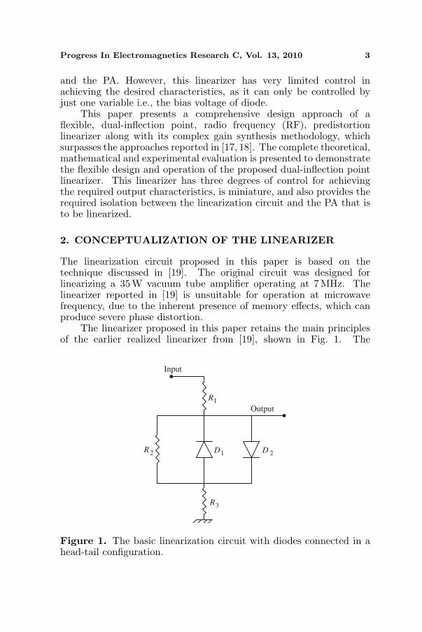
2. CONCEPTUALIZATION OF THE LINEARIZER
The linearization circuit proposed in this paper is based on thetechnique discussed in [19]. The original circuit was designed forlinearizing a 35 W vacuum tube amplifier operating at 7 MHz. Thelinearizer reported in [19] is unsuitable for operation at microwavefrequency, due to the inherent presence of memory effects, which canproduce severe phase distortion.
The linearizer proposed in this paper retains the main principlesof the earlier realized linearizer from [19], shown in Fig. 1. The
2D1D2R
1R
3R
Output
Input
Figure 1. The basic linearization circuit with diodes connected in ahead-tail configuration.

4 Hashmi, Rogojan, and Ghannouchi
proposed linearizer utilizes two Schottky diodes connected in a head-tail configuration and a p-intrinsic-n (PIN) diode in parallel with thetwo Schottky diodes. The novelty of the proposed linearizer lies inthe modifications, which allow it to become more flexible and adaptivefor linearization of traveling wave tube amplifiers (TWTAs), as well asmicrowave solid state power amplifiers (SSPAs).
The most basic linearization circuit with diodes connected ina head-tail configuration is depicted in Fig. 1. It consists ofsemiconductor diodes as a nonlinear resistor in a divider arrangement,as initially reported in [19]. This configuration, however, suffers fromlinear phase distortions. This phase distortion can compound theAM/PM characteristic observed in the PA that is to be linearized.To mitigate this effect, the linearizer could be tuned to resonance ata center frequency, but the linearizer is a nonlinear circuit; hence, theresonance cannot be achieved for the full range of input signals.
At microwave frequencies, the problem is more severe as thecapacitive effects of the junction capacitance, Cj , of the Schottkydiodes limit the usefulness of this linearizer to a very moderate rangeof input signals. To overcome this capacitive effect, the resonancecan be achieved by incorporating an appropriate inductance, Ls, inshunt, as shown in Fig. 2. With the incorporation of shunt inductance,Ls, the problem of linear phase distortion can be overcome for anyinput power and any bias voltage, Vsch, of Schottky diodes, D1 andD2. The actual bias voltage, VPK , across the Schottky diodes, D1 andD2, configuration is regulated by the bias feed resistances, Rb, and theinput RF power.
Output
Input
2D1D3DsL
c c
bR1bR
0QZ
schVpinV
c
PKV
λ/4
Figure 2. Configuration of the proposed linearizer circuit.
Progress In Electromagnetics Research C, Vol. 13, 2010 5
The PIN diode, D3, offers a variable resistance in shunt to theSchottky diodes, D1 and D2. It serves two purposes: on one hand,it provides a dynamic control to obtain the required gain and phasecharacteristics; while on the other hand, it also provides the improveddynamic range in the gain and phase responses, which are governed byits bias voltage, Vpin. The actual bias of the PIN diode is regulatedby the bias feed resistance, Rb1, and the input RF power. To ensurethe proper operation of the linearizer in the high impedance region ofthe Smith chart, a fixed resistor controls the PIN diode. The linearresistance is the net fixed resistor in parallel with the resistance ofthe PIN diode and ensures that the impedance of the linearizer duringoperation does not get near the center of the Smith chart, i.e., thecondition at which the linearizer loses the state of resonance.
The linearizer should have extremely low insertion loss and alsoexhibit very minimal phase dependent amplitude due to any residualdiode reactance. For this purpose, it is imperative that the impedanceof the diode configuration is transformed to a high value. The λ/4line has characteristic impedance sufficiently high to transform theimpedance of the semiconductor device approaching to an open circuit.The incorporation of the λ/4 line minimizes the phase dependentamplitude and also minimizes the insertion loss.
3. MATHEMATICAL ANALYSIS OF THE LINEARIZER
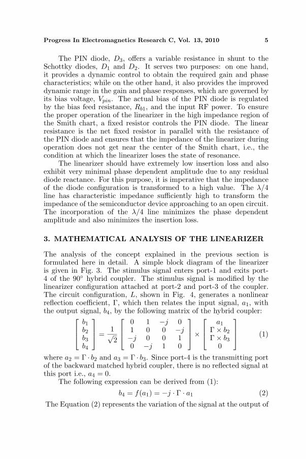
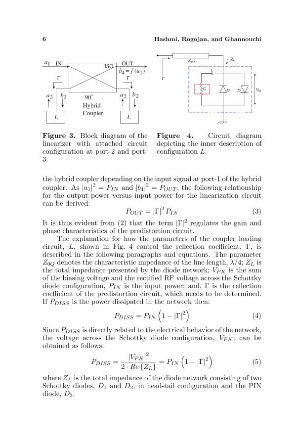
The analysis of the concept explained in the previous section isformulated here in detail. A simple block diagram of the linearizeris given in Fig. 3. The stimulus signal enters port-1 and exits port-4 of the 90◦ hybrid coupler. The stimulus signal is modified by thelinearizer configuration attached at port-2 and port-3 of the coupler.The circuit configuration, L, shown in Fig. 4, generates a nonlinearreflection coefficient, Γ, which then relates the input signal, a1, withthe output signal, b4, by the following matrix of the hybrid coupler:
b1
b2
b3
b4
=
1√2
0 1 −j 01 0 0 −j−j 0 0 10 −j 1 0
×
a1
Γ× b2
Γ× b3
0
(1)
where a2 = Γ · b2 and a3 = Γ · b3. Since port-4 is the transmitting portof the backward matched hybrid coupler, there is no reflected signal atthis port i.e., a4 = 0.
The following expression can be derived from (1):
b4 = f(a1) = −j · Γ · a1 (2)
The Equation (2) represents the variation of the signal at the output of
6 Hashmi, Rogojan, and Ghannouchi
90
1a
3a 3b 2b2a
IN OUTISO
LL
Γ Γ
o
Hybrid
Coupler
b = f (a )14
Figure 3. Block diagram of thelinearizer with attached circuitconfiguration at port-2 and port-3.
PKV1D 2DG
C
LZ0QZ
Γ
Figure 4. Circuit diagramdepicting the inner description ofconfiguration L.
the hybrid coupler depending on the input signal at port-1 of the hybridcoupler. As |a1|2 = PIN and |b4|2 = POUT , the following relationshipfor the output power versus input power for the linearization circuitcan be derived:
POUT = |Γ|2 PIN (3)
It is thus evident from (2) that the term |Γ|2 regulates the gain andphase characteristics of the predistortion circuit.
The explanation for how the parameters of the coupler loadingcircuit, L, shown in Fig. 4 control the reflection coefficient, Γ, isdescribed in the following paragraphs and equations. The parameterZ0Q denotes the characteristic impedance of the line length, λ/4; ZL isthe total impedance presented by the diode network; VPK is the sumof the biasing voltage and the rectified RF voltage across the Schottkydiode configuration, PIN is the input power; and, Γ is the reflectioncoefficient of the predistortion circuit, which needs to be determined.If PDISS is the power dissipated in the network then:
PDISS = PIN
(1− |Γ|2
)(4)
Since PDISS is directly related to the electrical behavior of the network,the voltage across the Schottky diode configuration, VPK , can beobtained as follows:
PDISS =|VPK |2
2 ·Re {ZL} = PIN
(1− |Γ|2
)(5)
where ZL is the total impedance of the diode network consisting of twoSchottky diodes, D1 and D2, in head-tail configuration and the PINdiode, D3.
Progress In Electromagnetics Research C, Vol. 13, 2010 7
If ZL is assumed to be real, then the above equation changes to:
|VPK | =√
2 · ZL · PIN
(1− |Γ|2
)(6)
The above equation can be solved for the estimation of the reflectioncoefficient, Γ.
The Schottky diodes are used in a head-tail configuration;therefore, the net current of this diode configuration is given by:
iD = IS
(eλ·v − 1
)− IS
(e−λ·v − 1
)= 2 · IS · sinh(λ · v) (7)
where iD is the diode current, IS represents the saturation current,and λ denotes a constant dependant on temperature (λ = q/n ·K ·T ).Where q is the charge on an electron, n is the ideality factor, K is theBoltzman constant and T is the absolute temperature of p-n junction.
For an input signal of VPK · cosω0t, the Blachman transforma-tion [20] can be employed to transform (7) into a summation of currentcomponents given by:
iD = 2 · IS
[ ∞∑
m=1
2Im (λVpk) cos(mω0t)
], m = 1, 3, 5 . . . (8)
where Im(λ · Vpk) is the modified Bessel function of first order for theinteger values of m.
The magnitude of the fundamental component of the diode currentcan be deduced from (8) and given by:
iD = 4 · IS · I1 (λVpk) (9)
The admittance of the Schottky diode configuration can now be definedas:
yD =iD (Vpk)
Vpk=
4 · IS · I1 (λVpk)Vpk
(10)
The total admittance, YTOTAL, of the network is the parallelcombination of yD; and, the shunt admittance of the PIN diode isdenoted by the parameter G.
YTOTAL = yD + G = G +4 · IS · I1 (λVpk)
Vpk(11)
Therefore, the total impedance of the diode network is given by thereciprocal of YTOTAL:
ZL =Vpk
G · Vpk + 4 · IS · I1 (λVpk)(12)
8 Hashmi, Rogojan, and Ghannouchi
The reflection coefficient, Γ, of the diode network can be writtenas:
Γ =Z2
0Q
ZL− Z0
Z20Q
ZL+ Z0
=Z2
0Q − Z0ZL
Z20Q + Z0ZL
(13)
where Z0 is the characteristic impedance of the system.Finally, the rearrangement of (12) and (13) gives the reflection
coefficient, Γ, in terms of the design parameters, Z0Q, G and Vpk:
Γ = |Γ|]φ =Z2
0Q [GVpk + 4ISI1 (λVpk)]− VpkZ0
Z20Q [GVpk + 4ISI1 (λVpk)] + VpkZ0
(14)
where |Γ| is the magnitude of the reflection coefficient and φ is thephase of the associated reflection coefficient.
The term |Γ|2 regulates the transfer characteristics as given in (3).It is thus evident from (14) that the transfer characteristics canbe controlled by varying the parameters impedance of the λ/4 line(ZOQ), the admittance of the PIN diode (G), and the voltage acrossthe Schottky diode configuration (VPK). The next section presentssimulation results to show the effects of the variation of the designparameters on the transfer characteristics of the linearizer, therebydemonstrating the flexibility of the operation of the proposed linearizer.
4. EVALUATION OF THE LINEARIZER CONCEPT
As previously described, the characteristics of the proposed linearizercan be controlled by i) varying the bias voltage across the Schottkydiode configuration; ii) the admittance of the PIN diode, i.e., the biasvoltage of the PIN diode; and, iii) the shunt inductance, Ls.
It can be deduced from (14) that the reflection coefficient, Γ, getssmaller with an increase in the bias voltage, VPK , of the Schottkydiode. The smaller Γ results in a smaller gain of the linearizer, as canbe seen in (3). This phenomenon is also evident in the results displayedin Fig. 5. It can thus be concluded that, by changing the bias voltagesof the Schottky diode configuration, Vsch, and at the same time keepinga fixed bias voltage of the PIN diode, Vpin, one can achieve the effectof delay in the conduction of the Schottky diode. The shifts in thetransfer characteristic along the axis of PIN is due to the presence ofseries bias feed resistance, Rb, shown in Fig. 2. This shift is due tothe increasing voltage drop across this bias feed resistance Rb with theincrease in RF input power, PIN . Therefore to maintain the Schottkydiode in conduction it will require higher Vsch than the value used atlow input power, and it is consistent with the result reported in [17].
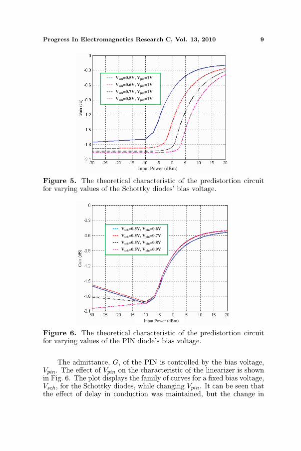
Progress In Electromagnetics Research C, Vol. 13, 2010 9
--- Vsch=0.5V, Vpin=1V
--- Vsch=0.6V, Vpin=1V
--- Vsch=0.7V, Vpin=1V
--- Vsch=0.8V, Vpin=1V
Input Power (dBm)
Figure 5. The theoretical characteristic of the predistortion circuitfor varying values of the Schottky diodes’ bias voltage.
--- Vsch=0.5V, Vpin=0.6V
--- Vsch=0.5V, Vpin=0.7V
--- Vsch=0.5V, Vpin=0.8V
--- Vsch=0.5V, Vpin=0.9V
Input Power (dBm)
Figure 6. The theoretical characteristic of the predistortion circuitfor varying values of the PIN diode’s bias voltage.
The admittance, G, of the PIN is controlled by the bias voltage,Vpin. The effect of Vpin on the characteristic of the linearizer is shownin Fig. 6. The plot displays the family of curves for a fixed bias voltage,Vsch, for the Schottky diodes, while changing Vpin. It can be seen thatthe effect of delay in conduction was maintained, but the change in

10 Hashmi, Rogojan, and Ghannouchi
the bias voltage of the PIN diode influenced the transfer characteristicfor low powers. The dynamic range of the linearizer can, therefore,be managed by controlling the bias voltage of the PIN diode; and,it eventually helps in achieving the required compression in the gaincharacteristics for the linearizer.
The impact of the varying shunt inductance, Ls, on the gaincharacteristics is shown in Fig. 7. The results show the gaincharacteristics of the linearizer for four different inductance values,while the bias voltage of all the diodes was kept at a fixed level.This family of curves shows no deviation; and, it clearly demonstratesthat the shunt inductance, Ls, resonates out the effect of the junctioncapacitance, Cj , of the Schottky diodes. Thus, the deployment ofan appropriate value for the shunt inductance, Ls, in the linearizermitigates the effect of Cj , which in turn prevents the linearizer frompossessing any memory effects. The selection of the value of Ls isregulated by the bias voltage of Schottky diodes, as the junctioncapacitance, Cj , is dependent on the bias voltage.
From the above analysis, it is apparent that the combined changesin the design variables provided a wide variety of control for the transfercharacteristics, thereby making the proposed linearizer very flexible. Ithas been demonstrated that the linearizer possesses three degrees offreedom; and, three different families of curves can be obtained with
--- LS=1 nH
--- LS=1.5 nH
--- LS=2 nH
--- LS=3 nH
Input Power (dBm)
Figure 7. The theoretical characteristic of the predistortion circuit forvarying values of the shunt inductance, Ls, while keeping Vpin = 0.8Vand Vsch = 0.6V.
Progress In Electromagnetics Research C, Vol. 13, 2010 11
this circuit for each situation, i.e., curves for the variation of the biasvoltage for the Schottky diodes, the bias voltage of the PIN diodes,and the shunt inductance, Ls. Based on the requirements, any orall of the parameters can, therefore, be altered to achieve the desiredcharacteristics.
5. DESIGN AND VALIDATION OF THE LINEARIZER
Through mathematical analysis and simulation, it has been establishedthat the proposed linearizer provides the flexibility for achieving thedesired characteristics by the variation of either bias voltages of theSchottky diodes or PIN diode, or by varying the shunt inductance, LS .It is shown in this section that careful consideration of the linearizer’sdesign and parameters allows it to obtain the two inflection points’ gaincharacteristics exhibited by a gallium arsenide field effect transistor(GaAs FET) device.
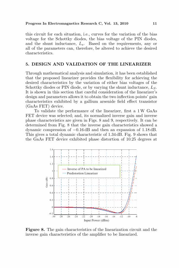
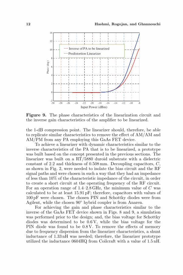
To validate the performance of the linearizer, first a 1 W GaAsFET device was selected; and, its normalized inverse gain and inversephase characteristics are given in Figs. 8 and 9, respectively. It can bedetermined from Fig. 8 that the inverse gain characteristics showed adynamic compression of −0.16 dB and then an expansion of 1.18 dB.This gives a total dynamic characteristic of 1.34 dB. Fig. 9 shows thatthe GaAs FET device exhibited phase distortion of 10.25 degrees at
-30 -28 -26 -24 -22 -20 -18 -16 -14 -12 -10 -8
-0.2
0
0.2
0.4
0.6
0.8
1
1.2
1.4
1.6
Pu issa nc e d'ent rée (dBm)
Gai
n (
dB
)
Input Power (dBm)
--- ---
Inverse of PA to be linearized
Predistortion Linearizer
Figure 8. The gain characteristics of the linearization circuit and theinverse gain characteristics of the amplifier to be linearized.
12 Hashmi, Rogojan, and Ghannouchi
-30 -28 -26 -24 -22 -20 -18 -16 -14 -12 -10 -8-2
0
2
4
6
8
10
12
14
Phas
e (d
eg)
Input Power (dBm)
---
---Inverse of PA to be linearized
Predistortion Linearizer
Figure 9. The phase characteristics of the linearization circuit andthe inverse gain characteristics of the amplifier to be linearized.
the 1-dB compression point. The linearizer should, therefore, be ableto replicate similar characteristics to remove the effect of AM/AM andAM/PM from any PA employing this GaAs FET device.
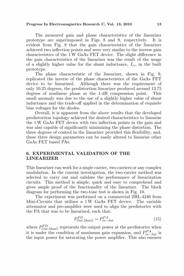
To achieve a linearizer with dynamic characteristics similar to theinverse characteristics of the PA that is to be linearized, a prototypewas built based on the concept presented in the previous sections. Thelinearizer was built on a RT/5880 duroid substrate with a dielectricconstant of 2.2 and thickness of 0.508mm. Decoupling capacitors, C,as shown in Fig. 2, were needed to isolate the bias circuit and the RFsignal paths and were chosen in such a way that they had an impedanceof less than 10% of the characteristic impedance of the circuit, in orderto create a short circuit at the operating frequency of the RF circuit.For an operation range of 1.4–2.8 GHz, the minimum value of C wascalculated to be at least 15.91 pF; therefore, capacitors with values of100 pF were chosen. The chosen PIN and Schottky diodes were fromAgilent, while the chosen 90◦ hybrid coupler is from Anaren.
For achieving the gain and phase characteristics similar to theinverse of the GaAs FET device shown in Figs. 8 and 9, a simulationwas performed prior to the design; and, the bias voltage for Schottkydiodes was determined to be 0.6 V, while the bias voltage for thePIN diode was found to be 0.8 V. To remove the effects of memorydue to frequency dispersion from the linearizer characteristics, a shuntinductance of 1.33 nH was needed; therefore, the linearizer prototypeutilized the inductance 0604HQ from Coilcraft with a value of 1.5 nH.
Progress In Electromagnetics Research C, Vol. 13, 2010 13
The measured gain and phase characteristics of the linearizerprototype are superimposed in Figs. 8 and 9, respectively. It isevident from Fig. 8 that the gain characteristics of the linearizerachieved two inflection points and were very similar to the inverse gaincharacteristics of the 1 W GaAs FET device. The slight difference inthe gain characteristics of the linearizer was the result of the usageof a slightly higher value for the shunt inductance, Ls, in the builtprototype.
The phase characteristic of the linearizer, shown in Fig. 9,replicated the inverse of the phase characteristics of the GaAs FETdevice to be linearized. Although there was the requirement ofonly 10.25 degrees, the predistortion linearizer produced around 13.75degrees of nonlinear phase at the 1-dB compression point. Thissmall anomaly was due to the use of a slightly higher value of shuntinductance and the trade-off applied in the determination of requisitebias voltages for the diodes.
Overall, it is apparent from the above results that the developedpredistortion topology achieved the desired characteristics to linearizethe 1W GaAs FET device with two inflection points in the gain andwas also capable of significantly minimizing the phase distortion. Thethree degrees of control in the linearizer provided this flexibility; and,these three design parameters can be easily altered to linearize otherGaAs FET based PAs.
6. EXPERIMENTAL VALIDATION OF THELINEARIZER
This linearizer can work for a single carrier, two carriers or any complexmodulation. In the current investigation, the two-carrier method wasselected to carry out and validate the performance of linearizationcircuits. This method is simple, quick and easy to comprehend andgives ample proof of the functionality of the linearizer. The blockdiagram for performing the two-tone test is shown in Fig. 10.
The experiment was performed on a commercial ZHL-4240 fromMini-Circuits that utilizes a 1 W GaAs FET device. The variableattenuator and pre-amplifier were used to align the predistorter withthe PA that was to be linearized, such that:
PPDOut MaxG = PPA
in−Sat (15)
where PPDOut MaxG represents the output power at the predistorter when
it is under the condition of maximum gain expansion, and PPAin−Sat is
the input power for saturating the power amplifier. This also ensures

14 Hashmi, Rogojan, and Ghannouchi
that the input power to the solid state power amplifier is the same aswhen the power amplifier is operated without the linearizer.
First, the power amplifier was excited by a single tone stimulus;and, the 1-dB compression point was found. For investigation andevaluation purposes, the two-carrier frequencies were chosen at f1 =1.625GHz and f2 = 1.635GHz. Then, the input power for the twotones was reduced in a symmetric manner; and, measurement wascarried out for the carrier output power along with the third- and fifth-order intermodulation distortion (IMD). The ratios of carrier outputpower to the respective third-order IMD, C/IMD3, and fifth-orderIMD, C/IMD5, are displayed in Figs. 11 and 12.
OutputInputLinearizer
Variable
Attenuator
Pre-
Amplifier
Linearization
System
Power
Amplifier
Figure 10. Block diagram of the linearization system for RFpredistortion.
2 4 6 8 10 12 1415
20
25
30
35
40
45
50
55
OPBO (dBm)
C/I
MD
3 (
dB
c)
ZHL-4240 before linearization
ZHL-4240 after linearization
---
---
Figure 11. C/IMD3 vs. OPBO for amplifier ZHL-4240 before andafter linearization.
Progress In Electromagnetics Research C, Vol. 13, 2010 15
2 4 6 8 10 12 1430
35
40
45
50
55
60
65
OPBO (dBm)
C/I
MD
5 (
dB
c)
ZHL-4240 before linearization
ZHL-4240 after linearization
---
---
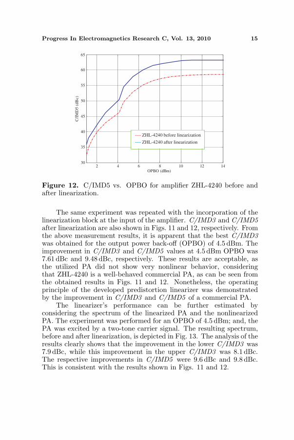
Figure 12. C/IMD5 vs. OPBO for amplifier ZHL-4240 before andafter linearization.
The same experiment was repeated with the incorporation of thelinearization block at the input of the amplifier. C/IMD3 and C/IMD5after linearization are also shown in Figs. 11 and 12, respectively. Fromthe above measurement results, it is apparent that the best C/IMD3was obtained for the output power back-off (OPBO) of 4.5 dBm. Theimprovement in C/IMD3 and C/IMD5 values at 4.5 dBm OPBO was7.61 dBc and 9.48 dBc, respectively. These results are acceptable, asthe utilized PA did not show very nonlinear behavior, consideringthat ZHL-4240 is a well-behaved commercial PA, as can be seen fromthe obtained results in Figs. 11 and 12. Nonetheless, the operatingprinciple of the developed predistortion linearizer was demonstratedby the improvement in C/IMD3 and C/IMD5 of a commercial PA.
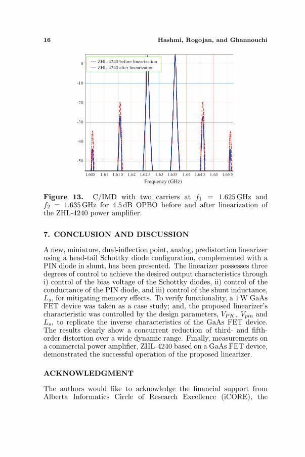
The linearizer’s performance can be further estimated byconsidering the spectrum of the linearized PA and the nonlinearizedPA. The experiment was performed for an OPBO of 4.5 dBm; and, thePA was excited by a two-tone carrier signal. The resulting spectrum,before and after linearization, is depicted in Fig. 13. The analysis of theresults clearly shows that the improvement in the lower C/IMD3 was7.9 dBc, while this improvement in the upper C/IMD3 was 8.1 dBc.The respective improvements in C/IMD5 were 9.6 dBc and 9.8 dBc.This is consistent with the results shown in Figs. 11 and 12.
16 Hashmi, Rogojan, and Ghannouchi
1.605 1.61 1.61 5 1.62 1.62 5 1.63 1.635 1.64 1.64 5 1.65 1.65 5
-50
-40
-30
-20
-10
0
Frequency (GHz)
ZHL-4240 before linearization
ZHL-4240 after linearization
---
---
Figure 13. C/IMD with two carriers at f1 = 1.625GHz andf2 = 1.635GHz for 4.5 dB OPBO before and after linearization ofthe ZHL-4240 power amplifier.
7. CONCLUSION AND DISCUSSION
A new, miniature, dual-inflection point, analog, predistortion linearizerusing a head-tail Schottky diode configuration, complemented with aPIN diode in shunt, has been presented. The linearizer possesses threedegrees of control to achieve the desired output characteristics throughi) control of the bias voltage of the Schottky diodes, ii) control of theconductance of the PIN diode, and iii) control of the shunt inductance,Ls, for mitigating memory effects. To verify functionality, a 1 W GaAsFET device was taken as a case study; and, the proposed linearizer’scharacteristic was controlled by the design parameters, VPK , Vpin andLs, to replicate the inverse characteristics of the GaAs FET device.The results clearly show a concurrent reduction of third- and fifth-order distortion over a wide dynamic range. Finally, measurements ona commercial power amplifier, ZHL-4240 based on a GaAs FET device,demonstrated the successful operation of the proposed linearizer.
ACKNOWLEDGMENT
The authors would like to acknowledge the financial support fromAlberta Informatics Circle of Research Excellence (iCORE), the

Progress In Electromagnetics Research C, Vol. 13, 2010 17
Natural Sciences and Engineering Research Council of Canada(NSERC) and Canada Research Chair (CRC) program. The authorsare also thankful to the staffs of the iRadio Lab for the technicalassistance.
REFERENCES
1. Helaoui, M. and F. M. Ghannouchi, “Linearization of power am-plifiers using the reverse mm-linc technique,” IEEE Transactionson Circuits and Systems II: Express Briefs, Vol. 57, No. 1, 6–10,January 2010.
2. Hammi, O., S. Carichner, B. Vassilakis, and F. M. Ghannouchi,“Synergetic crest factor reduction and baseband digital predis-tortion for adaptive 3g doherty power amplifier linearizer design,”IEEE Transactions on Microwave Theory and Techniques, Vol. 56,No. 11, 2602–2608, November 2008.
3. Kim, J., Y. Y. Woo, J. Cha, S. Hong, I. L. Kim, J. Moon,J. Kim, and B. Kim, “Analog predistortion of high power amplifierusing novel low memory matching topology,” Journal of the KoreaElectromagnetic Engineering Society, Vol. 7, No. 4, 146–153,December 2007.
4. Kursu, O., M. Riikola, J. Aikio, and T. Rahkonen, “Polynomial2.1GHz RF predistorter with envelope injection output,” SpringerAnalog Integrated Circuit and Signal Processing, Vol. 50, No. 1,13–20, January 2007.
5. Ma, H. and Q. Feng, “An improved design of feed-forward poweramplifier,” PIERS Online, Vol. 3, No. 4, 363–367, 2007.
6. Zhao, G., F. M. Ghannouchi, F. Beauregard, and A. B. Kouki,“Digital implementations of adaptive feedforward amplifierlinearization techniques,” IEEE MTT-S International MicrowaveSymposium, Vol. 2, 543–546, June 1996.
7. Eid, E. E. and F. M. Ghannouchi, “Adaptive nulling loopcontrol for 1.7-GHz feedforward linearization systems,” IEEETransactions on Microwave Theory and Techniques, Vol. 45, No. 1,83–86, January 1997.
8. Boulejfen, N., A. Harguem, and F. M. Ghannouchi, “New closed-form expressions for the prediction of multitone inter modulationdistortion in fifth-order nonlinear RF circuits/systems,” IEEETransactions on Microwave Theory and Techniques, Vol. 52, No. 1,121–132, January 2004.
9. Nakayama, M., K. Mori, K. Yamauchi, Y. Itoh, and T. Takagi,“A novel amplitude and phase linearizing technique for microwave
18 Hashmi, Rogojan, and Ghannouchi
power amplifiers,” IEEE MTT-S International Microwave Sympo-sium Digest, 1451–1454, Orlando, FL, May 1995.
10. Yamauchi, K., K. Mori, M. Nakayama, Y. Itoh, Y. Mitsui, andO. Ishida, “A novel series diode linearizer for mobile radio poweramplifiers,” IEEE MTT-S International Microwave SymposiumDigest, 831–834, 1996.
11. Gupta, N., A. Tombak, and A. Mortazawi, “A predistortionlinearizer using a tunable resonator,” IEEE Microw. WirelessCompon. Lett., Vol. 14, No. 9, 431–433, September 2004.
12. Katz, A., “Linearization: Reducing distortion in poweramplifiers,” IEEE Microwave, Vol. 2, 37–49, December 2001.
13. Hau, G., T. B. Nishimura, and N. Iwata, “A highly efficientlinearized wide-band CDMA handset power amplifier based onpredistortion under various bias conditions,” IEEE Transactionson Microwave Theory and Techniques, Vol. 49, 1194–1200, June2001.
14. Suematsu, N., T. Takeda, A. Lida, and S. Urasaki, “APredistortion type equipath linearizer in ku-band,” Proc. 3rd AsiaPacific Microwave Conf., 1077–1088, Tokyo, September 1990.
15. Wright, A. S. and W. G. Durler, “Experimental performance ofan adaptive digital linearized power amplifier,” IEEE Trans. Veh.Technol., Vol. 41, No. 4, 395–400, November 1992.
16. Ghannouchi, F. M. and J. S. Cardinal, “A new adaptive doubleenvelope feedback linearizer for mobile radio power amplifiers,”IEEE MTT-S International Microwave Symposium Digest, 573–576, San Diego, May 1994.
17. Yamauchi, K., K. Mori, M. Nakayama, Y. Mitsui, and T. Takagi,“A microwave miniaturized linearizer using a parallel diode witha bias feed resistance,” IEEE Transactions on Microwave Theoryand Techniques, Vol. 45, No. 12, 2431–2435, December 1997.
18. Park, C.-W., F. Beauregard, G. Carangelo, F. M. Ghannouchi,“An independently controllable AM/AM and AM/PM predis-tortion linearizer for CDMA2000 multi-carrier applications,”IEEE MTT-S International Microwave Symposium Digest, 53–56,Phoenix, May 2001.
19. Holbrook, G. W. and W. E. Rockwell, “Predistortion correction ofintermodulation products,” IEE Conf. Digest, 134–135, October1971.
20. Blachman, N. M., “Detectors, band pass nonlinearities, and theiroptimization: Inversion of the chebyshev transform,” IEEE Trans.Inf. Theory, Vol. 17, No. 4, July 1971.