Embed Size (px)
Citation preview

J. S. DunnD. C. Ahlgren
D. D. CoolbaughN. B. Feilchenfeld
G. FreemanD. R. Greenberg
R. A. GrovesF. J. GuarınY. HammadA. J. Joseph
L. D. LanzerottiS. A. St.Onge
B. A. OrnerJ.-S. RiehK. J. Stein
S. H. VoldmanP.-C. WangM. J. Zierak
S. SubbannaD. L. Harame
D. A. Herman, Jr.B. S. Meyerson
Foundationof rf CMOS andSiGe BiCMOStechnologiesThis paper provides a detailed description of the IBM SiGeBiCMOS and rf CMOS technologies. The technologies providehigh-performance SiGe heterojunction bipolar transistors(HBTs) combined with advanced CMOS technology and avariety of passive devices critical for realizing an integratedmixed-signal system-on-a-chip (SoC). The paper reviews theprocess development and integration methodology, presents thedevice characteristics, and shows how the development anddevice selection were geared toward usage in mixed-signal ICdevelopment.
1. IntroductionSilicon– germanium (SiGe) BiCMOS technology, whichachieved its first manufacturing qualification in 1996, isnow in its fourth lithographic generation of development.This class of technology integrates high-performanceheterojunction bipolar transistors (HBTs) with state-of-the-art CMOS technology. Key technology characteristicsfor the four generations have been reported by IBM [1– 4].All generations of BiCMOS technology are compatiblewith an associated IBM CMOS technology in devices,metallization (interconnects), and ASIC design system.Figure 1 is a SiGe BiCMOS chart showing the evolutionof performance and minimum lithographic feature sizetogether with some derivative technologies. As shownin Figure 2, the HBT cutoff frequency fT has improvedfrom 47 GHz in the 0.5-�m generation to 210 GHzin the 0.13-�m generation. The pace of developmentcontinues unabated, and there are no apparent barriersto scaling the SiGe HBTs beyond 210 GHz.
The SiGe HBT performance has been significantlyimproved by a combination of vertical and lateral scaling.Structural improvements included shrinking the emitterwidth and reducing layer thicknesses for the first threegenerations and migrating to a new raised extrinsic base(RXB) structure for the 0.13-�m generation. Verticalprofile scaling included increasing the drift field by
increasing the Ge concentration and reducing the gradedbase width, adding carbon (C) to decrease diffusion,reducing the thickness of the collector epitaxial layer,and minimizing the emitter thermal cycle. In the 0.13-�mgeneration, vertical and lateral profile scaling has led to areduction in the parasitics of the HBT, especially in thebase, collector, and emitter resistances (RB, RC, RE) andtotal collector– base capacitance (CCB). Coupled with theincreased fT, this reduction in parasitics is expected tolead to an increased fmax (the maximum frequency ofoscillation of a device, often referred to as U, forunilateral matched power gain, or MAG, for maximumavailable gain) in the devices. All devices in theproduction technologies must pass stringent quality andreliability tests [5]. Both the 120-GHz and 210-GHztechnologies exhibit collector– emitter breakdown voltagewith base open circuit (BVCEO) values around 2 V, but thisis not a serious concern, because in typical circuits thebase is biased through a finite resistance and the trueHBT breakdown voltage is between BVCER and BVCES
(typically between 3.5 V and 6.5 V. It is more importantto know the safe operation area and how large signalparameters vary as a function of use condition [6, 7].
In contrast to the trickle of early circuits [8], there isnow a flood of new SiGe products in almost every wiredand wireless application area. A sample of the wide
�Copyright 2003 by International Business Machines Corporation. Copying in printed form for private use is permitted without payment of royalty provided that (1) eachreproduction is done without alteration and (2) the Journal reference and IBM copyright notice are included on the first page. The title and abstract, but no other portions, of thispaper may be copied or distributed royalty free without further permission by computer-based and other information-service systems. Permission to republish any other portion of
this paper must be obtained from the Editor.
0018-8646/03/$5.00 © 2003 IBM
IBM J. RES. & DEV. VOL. 47 NO. 2/3 MARCH/MAY 2003 J. S. DUNN ET AL.
101

variety of SiGe BiCMOS circuits illustrates the wide-ranging applicability of these technologies (Table 1).
An important aspect of any SiGe BiCMOS technology isthe yieldable HBT device count. There are now products
with HBT device counts greater than 100 000. Agood example is a 68 � 69-cross-point switch1 whichcontains more than 100 000 SiGe HBTs. The largest chipto date is a 10.8 � 10.8-mm OC-48c SONET/SDH mapperwith integrated serializer/deserializer integrated clockrecovery (CDR) and clock synthesis (CSU).2 This highlyintegrated mixed-signal circuit includes 6000 HBTs and1.2 million CMOS transistors.
The 0.5-�m and 0.25-�m SiGe BiCMOS technologiesare ideal for many wireless applications. Areas of analogsections do not scale with decreasing lithography, whichreduces the incentive to migrate toward more advancedlithography ground rules [3]. Consequently, a full suiteof passive devices is required for any highly integratedmixed-signal chip. The focus in resistors is to achieve goodtolerance [�10% on polysilicon (poly) and single-crystalsilicon] and reduced parasitic capacitance. For the moststringent requirements, back-end-of-line (BEOL3) thin-film
1 AMCC S2090 preliminary data sheet, Applied Micro Circuits Corporation,6290 Sequence Drive, San Diego, CA 92121.2 AMCC S4803 preliminary data sheet.3 Those silicon chip process steps which occur beyond silicon device formationlevels (e.g., metal interconnects and interlevel dielectrics).
Figure 1
Summary of SiGe BiCMOS and rf CMOS technology.
Production
Production
Production
Production
0.5 m
3.3 V
0.5/0.35 m
3.3, 5 V
0.25 m
2.5 V
0.18 m
1.8 V
0.13 m
1.2 V
�
�
�
�
�
CMOS
lithography
120 GHz/1.8 V
30 GHz/4.5 V
200 GHz/1.7 V
TBD/TBD
60 GHz/3.0 V
40 GHz/4.0 V
30 GHz/6.0 V
47 GHz/3.3 V
27 GHz/5.7 V
20 GHz/9.5 V
50 GHz/3.3 V
25 GHz/7.0 V
5PA
50 GHz/3.3 V
27 GHz/5.5 V
5HP
Target >250 GHz/TBD
TBD/TBD
9HP
43 GHz/3.3 V
19 GHz/9.6 V
AM DM
DM
5MR/5HPE
8HP
7HP
7WL
6HP
5MR 5HPE
Main technology Derivative
Bipolar
High-speed npn fT
/BVCEO
High-breakdown npn fT
/BVCEO
Production
High performance
Derivative
1997 1998 1999 2000 2001 2002 2003 20041996
Figure 2
Cutoff frequency fT vs. I
C for four lithographic generations of
SiGe. The InP curve shows recent production InP results.
VCB
� 1 V
10�4 10�3 10�2
IC (A)
0
20
40
60
80
100
120
140
160
180
200
220
f T (
GH
z)
IBM SiGe
next
generation
InP low-current
best case
IBM 0.18- m
generation
IBM 0.5- m and 0.25- m generations � �
�
J. S. DUNN ET AL. IBM J. RES. & DEV. VOL. 47 NO. 2/3 MARCH/MAY 2003
102

Table 1 Circuits demonstrated using IBM SiGe technologies, showing their wide-ranging applicability and utility.
Application/Circuit Comments Figure of merit Reference
Model-hardware correlationRing oscillators ECL differential, typically
250 –300-mV swing5HP–16 ps7HP – 9 ps, 8HP – 4.2 ps
[8], Nortel(7HP, 8HP), unpublished
StoragePRML read channel Highly integrated BiCMOS
design�75 MB/s (600 Mb/s), product [2], IBM
RF/WLAN (2–2.5 GHz)Integrated VCO 0.5-�m SiGe, tuning using
MOS cap2.5 V, �95 dBc/Hz at 25 kHz,
9-mA core[9], IBM
TDMA power amplifier IS-54-compliant at 800 MHz [10], IBMCDMA power amplifier IS-95-compliant at 1800 or
1900 MHz[10], IBM
Wireless LAN chip set Three SiGe chips and oneCMOS chip to replaceeight GaAs chips
Commercial production part inPCM-CIA cards
[11], Intersil
Wireless down-converter 1-V design, integratedtransformer coupling andfeedback
Mixer 2.5 mA, LNA 2.5 mA at 1 V,LNA 10.5-dB gain, 0.9-dB noisefigure
[8], Nortel
2.5-GHz frequencysynthesizer
Three bipolar, four CMOSblocks (200 HBTs, 2500FETs, �150 passives)
�91 dBc/Hz at 100-kHz offset,2375–2550 MHz, 1-MHz spacing,44 mW core
[12], IBM
GPS chip set SiGe 0.5-�m BiCMOS Direct-conversion front end [13], IBM and SMI
Microwave/WLAN (5� GHz)Integrated VCO Fully integrated L, C,
varactor tankTo 26 GHz, 3 V, 22-mW core
power, 3.6% tune, 84 dBc/Hz at100-kHz offset
[14], IBM
Frequency divider 1.9-V, 0.5-�m SiGe BiCMOS 1.9 V, 220 �A, 2.3–5.9 GHz [8], NortelK-band static frequency
divider1/128, inductively peaked
input buffer, 0.5-�m SiGe23-GHz operation demonstrated [15], HRL
Base stationDigital, DAC chips 8-GHz clock, highly
integrated�140 dBc/Hz dynamic range [16], Siemens
NetworkingIntegrated VCO– 40G 0.18-�m SiGe, fully
integratedTo 25 GHz, digital coarse tuning
with MOS capacitors[17], IBM
Broadband amplifier 0.5-�m SiGe BiCMOSdesign
9-dB gain, 22-GHz BW, 6-dB NF [18], Nortel
Broadband amplifier For optical networkingreceiver
Up to 50 GHz bandwidth in 7HP [17], AMCC
High-gain amplifier 0.5-�m SiGe BiCMOSdesign
Integrated 60-dB stable gain for12.5G
[19], Nortel
Dynamic frequencydividers
Building block, divide by 2 5HP – 50 GHz, 7HP – up to 98GHz
Anonymous, unpublished
Multiplexer For SONET applications 5HP – 12.5 Gb/s, 7HP – 56 Gb/s [17, 20], IBMDemultiplexer For SONET applications Up to 45 Gb/s [17, 20], IBMSer/Des 0.5-�m single-chip solution 12.5 Gbaud [21], IBMModulator driver Distributed large-signal
amplifierUp to 48 Gb/s, 3.5 V peak-to-peak AMCC data sheet
Network switch 68 � 69, 150 000 SiGe HBTs 2.5 Gb/s, �200 Gb/s throughput AMCC data sheet10-Gb/s chip set Complete chip set for
STM64/OC-192 designedby Alcatel
Mux and demux, laser driver,preamp, limiting amp, CDR(data recovery)
[22], Alcatel
Data conversionD-to-A converter Analog Devices design 12 bits, �1 GSample/s [23], ADIA-to-D converter IBM Research 4 bits, 8 Gsample/s [24], IBM�� modulator Fourth-order, 0.5-�m SiGe,
LC resonators with Qenhancement
5 V, 350 mW at 4 GHz, max SNR53 dB, SFDR 69 dB (11 bits)
[25], Carleton University
Continued on next page
IBM J. RES. & DEV. VOL. 47 NO. 2/3 MARCH/MAY 2003 J. S. DUNN ET AL.
103

resistors are being added [3]. The thrust for varactors isimproved tunability, while maintaining linearity, and highQ (quality factor) values. Capacitors, both front-end-of-line (FEOL) MOS and metallization-based MIM, requirehigher capacitance per unit area to provide analog areascaling. The performance of spiral inductors continuesto be improved by thick metals in spite of skin-effectconcerns. Further enhancements include multiple layers ofthick metal, deep-trench mazes under the inductor, andpolysilicon ground shields.4 These features, which arediscussed in detail in the section devoted to passiveelements, result in passives that are much better thanthose in conventional silicon CMOS and similar topassives in GaAs ICs.
Although the SiGe HBT transistor is the cornerstone ofIBM BiCMOS technologies, many components contributeto their success. Moreover, there are applications whichdo not require the performance provided by the SiGebipolar transistor. This application space was addressedby developing rf CMOS technologies as derivatives ofthe SiGe BiCMOS technologies. The first of these tobe qualified, 0.25-�m CMOS 6SFRF, is based on theBiCMOS 6HP and CMOS 6SF technologies. RF CMOStechnologies include an extensive suite of passive devices,device models optimized for radio frequency (rf)applications, and a design automation system which iscompatible with rf design techniques. For CMOS devices,high-quality passives are critical in achieving a system on a
chip (SoC), because of the difficulty of rf matching MOSdevices. More advanced rf CMOS technologies are alsobeing developed with minimum linewidths of 0.13 �m and0.10 �m.
This paper first reviews the active devices (npn HBTand MOS FETs) and passive devices (resistors, capacitors,varactors, and inductors) available in these technologies indetail from a circuit designer’s point of view. We presentdc and ac figures of merit important for high-performancemixed-signal communications technologies. The tradeoffsinvolved in device design are also discussed. Includedin this section is a discussion on the importance ofelectrostatic discharge (ESD) technology, with specialrequirements for rf applications. The next section coverstechnology development methodology for SiGe BiCMOSand rf CMOS devices. We discuss the qualificationmethodology and manufacturability of (Bi)CMOS mixed-signal rf technologies. This is followed by a discussion ofother technology issues that have implications for circuitand product design. Noise, isolation, and active devicereliability are discussed in detail, as well as metalelectromigration, which is important for design of areliable product.
2. Devices for communications technologies
SiGe HBT overviewThe addition of Ge into the bipolar junction transistor(BJT) by IBM in the late 1980s, creating a heterojunctionbipolar transistor, or HBT, enabled higher performance4 D. Coolbaugh, IBM internal communication.
Table 1 Continued.
Application/Circuit Comments Figure of merit Reference
MemoryBipolar cache RPI design 0.3 ns access time [26], RPI
Ultrawide bandTiming generator chip 0.5-�m SiGe HBT design 5 V, 0.5 W, up to 2.5 GHz,
2 ps accuracy, 10 ps jitter in a100-ns window
[27], TDSI/SMI
InstrumentationPin electronics driver [28], IBM
DigitalRISC engine Simulation/analysis of
methods to achieve�16-GHz RISC engine
SiGe higher HBT count and CMOSintegration has major benefits
[29], RPI
Highly integratedOC48 mapper 0.5-�m SiGe BiCMOS 2.5 Gb/s highly integrated [11], AMCCASIC test site 1.8M CMOS, ASIC
qualification vehicleEquivalent to base 0.5-�m CMOS [30], IBM
RadarX-band phase shifters PIN diode circuits with thick
metal add-on module(Hughes/Raytheon)
2- and 3-bit fully integrated phaseshifters at 6 –10 GHz
[11], Hughes/IBM
J. S. DUNN ET AL. IBM J. RES. & DEV. VOL. 47 NO. 2/3 MARCH/MAY 2003
104

than was believed possible in silicon technologies. Afundamental reason for using a BJT is its exponentialchange in output current with input voltage. At its peakoperating point, the BJT achieves about three timesthe transconductance, and thus three times the drivecapability, of an FET, as illustrated in Figure 3. Retainingthe beneficial properties of the BJT, the incorporation ofGe into the base of the device introduced a number offurther benefits.
Incorporation of substitutional Ge into the crystallattice of the silicon creates a compressive strain in thematerial (because the Ge atom requires a larger atomicseparation), and as a result, reduces the bandgap of thematerial. In a typical HBT (as in GaAs or InP materials),this bandgap difference between layers of semiconductormaterials is used to affect the injection of carriers betweenthe two sides of the junctions. Some SiGe HBTs aresimilar, where the Ge is formed in an abrupt transitionto a constant value over a specified width. In the IBM“graded” SiGe HBTs, the Ge content is not a constant,but instead increases (low concentration closer to thewafer surface to high concentration deeper into thedevice) and thus contains a decreasing bandgap in thedirection of electron flow. Figure 4 is a schematic diagramof the Ge concentration and associated band structureillustrating this concept. The electrons are injected fromthe emitter of the device, having a reduced barrier toinjection because of the small Ge content at the junction,and then experience an accelerating field from theincreasing Ge content deeper into the device. Theelectrical effects of this graded Ge content are welldocumented [31]. The content at the junction increasesthe electron injection into the base, thus increasing thedc current gain. The Ge grade has the effect of speedingthe transport of electrons across the device, resulting inhigher-frequency operation. The Ge grade also improvesthe device Early voltage (flatness of the output current asa function of output voltage characteristics) by modulatingthe intrinsic carrier concentration across the base. TheGummel characteristic [Figure 5(a)] illustrates the factthat the turn-on voltage for a SiGe HBT comparesfavorably with III–V HBT devices, and the outputcharacteristic [Figure 5(b)] illustrates very flatcharacteristics and a sharp “knee,” both favorable to highvoltage gain in such a device. The aspect of accelerationof electrons across the device is one of particularimportance in scaling the device to higher-speedperformance, as is discussed shortly.
HBT device designToday, IBM is engaged in a number of SiGe HBTdevice design activities, driven by markets with differingrequirements (see the summary of HBT characteristicsin Table 2). Even though high-speed performance often
gets the attention in SiGe HBT device developments,advances are taking place to address applications that donot demand higher speed but rather higher-voltageoperation or lower costs.
Semiconductor chips used in wireless applicationssuch as cellular phones, wireless networks, and globalpositioning systems (GPSs) are required to be inexpensive.The number of masks and the complexity of processingaffect wafer cost and yield, and therefore the finalpackaged part cost. To achieve cost reductions, waferprocessing is simplified by reducing the number of processsteps. These reductions can take the form of eliminatinga portion of the structure (deep-trench isolation),consolidation of masking steps, or changes to the HBTstructure [non-self-aligned (NSA) extrinsic base]. In all
Figure 3
Bipolar junction transistor (left), with three times higher trans-
conductance, more effectively drives a parasitic load than a field-
effect transistor (right).
Parasitic load the same
FET
~1 mS/ m
BJT
~3 mS/ m � �
Figure 4
Ge concentration (bottom) and band structure (top) of a SiGe
heterojunction transistor. The Ge provides a lower barrier to
injection from emitter to base as well as an accelerating field
through the base.
Emitter
Germ
aniu
m
conte
nt
Base Collector
Energ
y (e
V)
n p n
Si
SiGe
F
V
C
e�
e�
e�
IBM J. RES. & DEV. VOL. 47 NO. 2/3 MARCH/MAY 2003 J. S. DUNN ET AL.
105

situations, the device performance is altered as part of thedevice customization required for a particular end use.
An example of the cost/performance tradeoff isillustrated by the SiGe 5MR technology, which wastailored for the �5-V supply voltage used by hard diskdrive preamplifiers. These enhancements were alsoincorporated into SiGe 5HPE. Again, the chip cost was
required to be low, and the challenge was to meet boththe cost and use voltage criteria simultaneously. Whilethe higher BVCEO target (9.6 V) was met by increasing thelightly doped collector epitaxial layer thickness, the outputcharacteristics of the high-breakdown HBT suffered frombarrier effects [32] caused by base broadening, as shown inFigure 6(a). The usual high values of Early voltage were
Table 2 HBT characteristics across generations of BiCMOS technology.
Units 5HP 5HPE 6HP 7HP 8HP
npn isolation Deep trench Shallow trench Deep trench Deep trench Deep trench
Peak fT GHz 50 45 50 120 210Peak fmax 65 50 65 100 185
fT at 30 �A(min. area)
GHz 15 19 19 25 50
IC at peak fT(min. area)
mA 0.6 0.5 0.5 1.0 1.0
BVCEO V 3.3 3.3 3.3 2.0 1.9
BVCBO V 10.5 10.5 10.5 6.5 6
Peak fTHigh-BV npn
GHz 29 17 29 20 —
BVCEOHigh-BV npn
V 5.5 10.0 5.0 4.7 —
BVCBOHigh-BV npn
V 14.0 20.5 14.0 12.5 —
npn density(min. area)
relativeunits
1� 1� 1.7� 2.0� 2.0�
10�2
10�3
10�4
10�5
10�6
10�7
10�8
10�9
0.4 0.6 0.8 1 1.2 1.4
Coll
ecto
r curr
ent
densi
ty (A
/ m
2)
InP
SiGe
GaAs
0.0
0.5
1.0
1.5
2.0
2.5
3.0
0 1 2 3 4V
CE (V)
(b)
VBE
(V)
(a)
I C (m
A)
�
Figure 5
(a) Gummel characteristic of SiGe HBT demonstrates linear characteristics and low turn-on voltage. (b) Output characteristic demonstrates
flat IC versus V
CE, enhancing voltage gain in applications.
J. S. DUNN ET AL. IBM J. RES. & DEV. VOL. 47 NO. 2/3 MARCH/MAY 2003
106

compromised. Two approaches were taken to improvetransistor performance: 1) improve the base Ge profileby introducing the boron within the Ge base layer, and2) increase the lateral spacing between the extrinsicbase implant with respect to the emitter opening, thusdecreasing enhanced diffusion of the intrinsic basecaused by the extrinsic base implant [33]. These twoimprovements resulted in a substantially improved VA, asshown in Figure 6(b). In addition, the peak frequencyperformance, fT, was improved from 14 GHz to 19 GHz.
With an increased distance from the extrinsic baseimplant to the emitter opening, it was more cost-effectiveto simplify the usual self-aligned extrinsic base structure toa NSA version in which the emitter polysilicon itself wasused as the mask for the extrinsic base implant. A 7%reduction in processing time and an equally substantialreduction in wafer cost were achieved. These deviceimprovements were feasible because the circuit designerswere willing to trade off higher base resistance forincreased frequency performance and Early voltage.Owing to the less complex emitter definition process, theVBE matching is also markedly improved. These devicetradeoffs meet both the circuit design and wafer costrequirements and demonstrate the versatility of thesuccessful IBM SiGe technologies.
In the high-speed arena, SiGe HBTs today aresurpassing even the fastest III–V production devices. Thekey to this achievement is the superior within-deviceparasitic-control technology available to SiGe devicedesigners, compared to what is available to III–V devicedesigners. With lithographically defined implants, trenchisolation, self-aligned low-resistance regions, and optionssuch as spacer technology, silicon device designers have amyriad of tools at their disposal.
The most common measure of performance is fT,which is the maximum frequency at which the transistordemonstrates useful (i.e., above unity) current gain. Thecomponents of fT are the diffusion capacitance chargingrelation (kT/qIE)(CEB � CCB), transit times across thedevice (principally consisting of base transit time �B andcollector space-charge transit time �C), and the collectorresistance– collector base capacitance RCCCB charging time,as shown in Equation (1):
1/2�fT � �EC � kT/qIECEB � CCB � RCCCB � �B � �C .
(1)
Improvements in fT are achieved by reducing the thicknessof each of the layers through which the electrons musttravel—the neutral base (i.e., affecting �B) and thecollector space-charge region (i.e., affecting �C), as wellas reducing the RC charging terms for the parasiticcapacitances in the device. This concept is shown inFigure 7(a). The distribution of the boron dopant (which
comprises the base) is made narrower; the Ge distributionis also made narrower, and the grade is increased; also, the
Figure 6
Output characteristics (a) prior to and (b) following Ge profile
and extrinsic base modifications in the 5HPE technology.
0 2 4 6 8 100.0
1.0 � 10�4
2.0 � 10�4
3.0 � 10�4
4.0 � 10�4
5.0 � 10�4
6.0 � 10�4
7.0 � 10�4
0.44 � 3 high breakdown device
1 A/IB step
0 2 4 6 8 100.0
1.0 � 10�4
2.0 � 10�4
3.0 � 10�4
4.0 � 10�4
5.0 � 10�4
6.0 � 10�4
7.0 � 10�4
VCE
(b)
VCE
(a)
I C (
A)
I C (
A)
�
0.44 � 3 high breakdown npn
0.25 A/IB step�
Figure 7
Vertical scaling of the graded-base SiGe HBT: (a) Dopant profile
is made more narrow for reduced transit time and reduced
collector resistance. (b) Relationship between fT and current
density.
Current density
(b)
Depth
(a)
Increase
Ge slope
Narrow
base
Collector
Reduce
transit
time
Suppress
Kirk effect
for higher
current
Concentr
ati
on
f T
IBM J. RES. & DEV. VOL. 47 NO. 2/3 MARCH/MAY 2003 J. S. DUNN ET AL.
107

collector concentration is increased, which reduces thethickness of the space-charge region and at the same timereduces the collector access resistance. We refer to this asvertical scaling of the transistor, since these aspects arenot related to the lateral dimensions of the device. Theresult of vertical scaling is to reduce the transit time andincrease the maximum operating current density in thedevice (i.e., for the same size device, the current to reachmaximum fT performance is increased). Figure 7(b) showsthis effect of vertical scaling on a plot of fT vs. currentdensity.
The second common measure of performance is fmax,which is the maximum frequency at which the transistorhas useful (i.e., above unity) power gain; fmax isapproximately given by the well-known relationshipbetween fT and parasitics,
fmax � fT/8�RBBCCB 1/ 2, (2)
where RBB and CCB are respectively the parasitic baseresistance and collector– base capacitance. For mostapplications, it is required that the fmax value be atleast comparable to the fT value for optimal circuitperformance. Achieving high fmax is a challenge from thepoint of view of both device design and process, since it isa strong function of the device structure, which largelydetermines the values of RBB and CCB. This is because themajority of RBB and CCB are present in the extrinsic partof the device, or that region of the device which is not anessential part of the carrier transport. This fact provides
the expectation that fmax will continue to be substantiallyimproved with new device structures.
Comparison of the IBM SiGe HBT device structuresillustrates how improvements in device structure mayprovide increases in the figure of merit, fmax. Throughseveral generations of technology, IBM has utilized thesame device structure, often referred to as the epitaxialtransistor (ETX). Its identifiable structural characteristicis an extrinsic base implanted into the SiGe epitaxialfilm. Through careful analysis, depending heavily on 2Dsimulations [34], it was determined that this structure hassome significant limitations. Implants into the siliconcreate lattice defects, which affect the diffusion of theintrinsic base boron, increasing �B and thus reducingdevice performance. This limits how close the implant maybe placed to the intrinsic device, and therefore creates alower limit on the achievable base resistance, RBB.The implanted extrinsic base also extends deep intothe silicon and intersects the collector implants at a highconcentration, which results in high CCB. Shown in Figure 8are the ETX structure and the structure IBM is pursuingwith a raised extrinsic base (RXB) to substantially reduceRBB and CCB. The raised extrinsic base has less influenceon the intrinsic dopant diffusion and may be placed inclose proximity to the intrinsic device, thus reducing RBB
without impact to fT. It also has a minimal junction depth,and, as such, has a relatively small CCB.
Initial results on the RXB structure demonstrate itsbenefits over the ETX structure. While retaining the fT
performance of a structure without a self-aligned extrinsicbase (indicating no influence of the extrinsic base on theintrinsic base), the base resistance has been reduced by afactor of approximately 2, and CCB has been maintainedconstant compared to a previous-generation device ofsimilar area, with lower fT. This results in simultaneous fT
and fmax improvements between generations of more than80% (Figure 9).
FETs and their utilityThe CMOS device takes on different roles whetheroffered as part of a BiCMOS technology, where thebipolar device is available for analog functions, or as partof a CMOS-only technology, where the FET devicesmust take a primary role in analog functionality. Fromdevice design, device layout, process development,characterization, and modeling, this differentiationinfluences technology development. This section discussesnot only the digital design aspects of FET devices, butalso aspects that are driven by analog requirements, suchas the ability of these devices to withstand higher voltagesor have lower back-bias sensitivity (body effect) or higherself-gain ( gm/g0). These aspects were less important inBiCMOS processes because of the presence of the bipolar
Figure 8
ETX structure (top) and RXB structure (bottom). The RXB
structure eliminates the unwanted effects from the deep implant,
including the excess capacitance and diffusion effects on the
intrinsic base region.
Collector implant
Implanted
extrinsic
base
Raised
extrinsic base
SiGe intrinsic base
High-
capacitance
region
Influence of
implant damage
on intrinsic base
J. S. DUNN ET AL. IBM J. RES. & DEV. VOL. 47 NO. 2/3 MARCH/MAY 2003
108

device, but in CMOS-only technologies they become moreessential. Thus, one finds as a requirement that additionalmasks and complexity be present in CMOS processes,and a greater variety of FET devices are offered todesigners.
When offered as part of IBM SiGe BiCMOStechnologies, the CMOS devices are used primarily forintegrating digital logic functions with high-speed bipolaranalog circuits. This allows fully integrated system-on-a-chip products, with the CMOS performing the lower-frequency baseband signal processing. The logicfunctionality is streamlined by offering ASIC libraryelements from the base CMOS technology to beintegrated with the rf analog circuits. The CMOS devicescan also be used for low-frequency analog functions suchas A-D converters, multiplexers, and switches. CMOSdevices have one large advantage over bipolar devices:There is essentially no gate current. This makes CMOSdevices ideal in circuits where it is required to measurethe charge on capacitors such as A-D converters. Bipolardevices would drain the charge during the measurement.
Development of CMOS devices for digital logicpurposes is driven primarily by shrinking the devicedimensions, thinning the gate oxide, and lowering supplyvoltages to achieve faster performance, increased density,and lower power consumption. The smaller device lengthslower the parasitics and increase fT, but also necessitatecomplex designs including halo implants to minimizeshort-channel effects and control punch-through. Theseimplants have negative effects on important analogcharacteristics such as self-gain ( gm/g0). Also, thethinner gate oxides in the advanced logic devices cannotsupport the higher voltages required in analog circuits.Additionally, gate current becomes non-negligible. Thesolution to this is a dual-oxide technology. The analogdevices are designed with thicker oxides, longer channellengths, and unique source/drain extensions. This addedprocess complexity allows placement of high-performancelogic devices and high-voltage analog devices on the samechip.
Some specific parameters such as noise and Vt matchingmust be considered when designing analog CMOS devices.Noise is not a large concern in digital CMOS circuits, andsome processes such as nitrided gate oxide actuallyincrease noise in a tradeoff for decreased dopantpenetration of the gate oxide and improved hot-carrierdegradation. Vt matching in analog circuits is muchmore critical than in logic circuits, and all variablesthat introduce mismatch, including process and layout,must be minimized.
IBM has four SiGe BiCMOS technologies and oneCMOS rf technology qualified for high-volume production:
SiGe 5HP, SiGe 5HPE, SiGe 6HP, SiGe 7HP, and CMOS6SFRF. SiGe 5HP and SiGe 5HPE are single-gate-oxidetechnologies, while the rest have an optional dual-gate-oxide process. SiGe 5HP contains 3.3-V CMOS devicesdesigned specifically for logic support in the BiCMOStechnology. SiGe 5HPE has a 12-nm gate oxide, 5-V CMOSwith an additional isolated n-FET device. The iso-n-FETis a standard n-FET surrounded by an isolation tub whichallows the iso-n-FET p-well to be biased independentlyfrom the substrate. Independent well biasing enables acircuit designer to handle dual logic levels on-chip, forexample by biasing the substrate at �5 V and the p-wellin the tub at 0 V. Higher-voltage analog signals can alsobe handled in this way by stacking 5-V FETs insideand outside the isolation, with a 10-V signal across thecombination. Iso-n-FET devices also have better noiseisolation owing to the independently biased p-well andisolation tub.
The dual-oxide technologies are SiGe 6HP, CMOS6SFRF, and SiGe 7HP. SiGe 6HP contains 2.5-V and3.3-V CMOS devices, which have 5-nm and 7-nm gateoxides, respectively. The thin-oxide FETs, with 0.25-�m Lmin
(minimum drawn gate lengths), are used for the high-speed logic, while the thick-oxide devices are 0.4-�m-Lmin
n-FETs and 0.34-�m-Lmin p-FETs. The thick-oxide FETsenable 3.3-V I/O compatibility as well as analog signalhandling. CMOS 6SFRF is based on the same 2.5-V/3.3-Vdevices, with an additional 2.5-V iso-n-FET and a processoption of 6.5-V thick-oxide (14-nm) devices in place of the3.3-V devices. The 6.5-V devices have Lmin � 0.7 �m tosupport the higher voltage. These devices can be used
Figure 9
Comparison of cutoff frequencies between SiGe 7HP fT � 120-
GHz device with ETX structure and next-generation fT � 210-
GHz device, with vertically scaled profile and new RXB
structure. (MAG � maximum available gain; U � unilateral
matched power gain.)
0
50
100
150
200
250
300
10�4 10�3 10�2 10�1
Collector current (A)
Cuto
ff f
requencie
s f T
, f M
AX
(G
Hz)
Next-generation
BiCMOS 8HP
Production
BiCMOS 7HP
U fMAX
VCB
� 1 V, 25C
fT
MAG
fMAX
IBM J. RES. & DEV. VOL. 47 NO. 2/3 MARCH/MAY 2003 J. S. DUNN ET AL.
109

as low-frequency power amplifiers (amps), high-voltageanalog switches, and voltage regulators in battery chargers.SiGe 7HP has 1.8-V and 3.3-V CMOS devices with 3.5-nmand 6.8-nm gate oxides, respectively. There are 1.8-Vstandard-Vt FETs and optional 1.8-V high-Vt FETs, 3.3-VFETs, and both 1.8-V and 3.3-V iso-n-FETs. The 1.8-VFETs have Lmin � 0.18 �m and the 3.3-V FETs haveLmin � 0.4 �m. Table 3 compares some of the keyparameters of each technology.
The main purpose of the CMOS devices in a BiCMOStechnology is to provide integrated logic functionality.The logic design can be expedited by using ASIC library“books” already developed for the base CMOS technology.This approach can be used only if the CMOS devicecharacteristics in the BiCMOS technology closely matchthose of the base CMOS technology. Many processdifferences can lead to significant device differences.Adjusting the process minimizes many of thesedifferences, but some cannot be corrected. To verify thatthe ASIC library elements function correctly and thatthe CMOS timing models are still valid for the BiCMOSprocess, ASIC library test sites are built in the BiCMOSprocess. The chips are tested for functionality, andhardware-to-model correlation is done to validate thetiming models. Because some devices are known notto function correctly owing to process differences, anylibrary elements containing these devices are not tested.In Figure 10, a typical correlation plot with both SiGeand CMOS data shows that the same model canaccurately represent both technologies.
Figure 10
Box plot showing SiGe 6SF CMOS performance sort ring
oscillator (PSRO) (2) identical to CMOS 6SF Longtrail hardware
(1).
Table 3 Comparison of thin-oxide CMOS parameters for SiGe BiCMOS and rf CMOS technologies.
Parameter Units SiGe 5HP SiGe 5HPE SiGe 6HP SiGe 7HP CMOS 6SFRF
n-FET p-FET n-FET p-FET n-FET p-FET n-FET p-FET n-FET p-FET
TOX (thin) nm 7.8 12.0 5.0 3.5 5.0
TOX (thick) nm — — 7.0 6.8 7.0/14.0
VSUPPLY V 3.3 5 2.5/3.3 1.8/3.3 2.5/3.3/6.5
Lmin �m 0.5 0.5 0.25 0.18 0.25
LEFF �m 0.39 0.36 0.4 0.45 0.19 0.18 0.12 0.14 0.18 0.18
VT lin mV 600 �550 820 �740 500 �500 355 �420 500 �500
ID sat �A/�m 480 213 600 265 595 280 600 260 595 280
IOFF nA/�m 0.1 0.1 0.004 0.003 0.005 0.003 0.1 0.05 0.005 0.003
Body effect 0.34 0.35 0.15 0.23 0.23 0.27 0.19 0.25 0.23 0.27
gm sat �S/�m 195 103 165 78 300 200 500 275 300 200
fT GHz 20 10 19 9 35 20 75 45 35 20
fmax GHz 22 17 — — 22 22 70 45 22 22
J. S. DUNN ET AL. IBM J. RES. & DEV. VOL. 47 NO. 2/3 MARCH/MAY 2003
110

High-quality passive components critical forcommunications circuitsBiCMOS technology development in IBM has beenfocused largely on the integration of high-performanceSiGe HBTs in a base CMOS technology. In general,passive devices are developed from existing processesused for these transistors; i.e., resistors are formed fromCMOS FET source/drain implants, MOS capacitors fromthe reach-through implants used for the HBT collectorcontact and FET gate oxide/polysilicon gate, and inductorsdesigned using last-metal options for these technologies.The need for high integration and technology innovationin rf circuit design has changed the direction of passivedevelopment in the last several years. Passive deviceswhich in some cases utilize processes not used fortransistor manufacture have allowed the developmentof high-performance devices enabling rf technologyinnovations. Examples are thick analog metals (AMs), e.g.,4-�m Al, used as last-metal options for high-Q inductors;TaN resistors integrated in the back-end-of-line (BEOL)metallization for low parasitic capacitance/tolerance; andhigh-capacitance nitride metal-insulator-metal (MIM)capacitors.
Balancing the performance of passive devices withprocessing costs is a challenge. Some of the more criticalparameters for the passive elements used in rf designsare resistor tolerance, varactor tunability (Cmax/Cmin) andlinearity, MIM capacitance density and quality factor (Q),and inductor Q. In the following sections, the importantpassive elements offered in the IBM SiGe BiCMOS andrf CMOS technologies are described, with focus on theirrf application, key figures of merit, and reliability.
ResistorsResistors are used in all analog and mixed-signal circuitblocks. A wide variety of resistors are offered in theIBM SiGe BiCMOS and rf CMOS technologies toaccommodate designer needs (see Table 4). Figures ofmerit for resistors are sheet resistance, tolerance, parasiticcapacitance, voltage, and temperature coefficients. Threetypes of basic resistors are used in the SiGe BiCMOSprocess to achieve the desired properties and resistanceranges needed in analog circuit designs: p-doped
polysilicon resistors, n- and p-type diffusion resistors,and BEOL TaN metal resistors.
Highly doped p-type polysilicon resistors are preferredin most cases for mixed-signal and analog applicationsbecause of their good matching, low parasitic capacitanceto the substrate, and excellent temperature coefficient,as shown in Table 4. These resistors consist of gate orSiGe polysilicon doped with a high-dose boron implant,normally the p-FET source/drain implant. Either shallow-trench isolation or shallow/deep-trench isolation is usedunder these resistors to reduce parasitic capacitancebetween the resistor and substrate. The ends of theresistor are silicided for low contact resistance to theBEOL wiring, and the body of the resistor is covered withsilicon nitride to block the silicide. The p� polysiliconresistor has a sheet resistance of 270 �/� and a 10 –15%tolerance. Low tolerance is essential for efficient compactcircuit designs. Table 4 shows that this resistor has a verylow temperature coefficient (TCR) of 21 ppm/ C, which is2–3% the TCR of the other resistors offered. This makesthe resistor most attractive for circuit applications owingto low variation in resistance with changes in temperatureover typical ranges of �40 C to 125 C. The parasiticcapacitance between the resistor and substrate is 10% ofthat of a diffusion resistor but four times the value for aBEOL resistor because of the distance of these devicesfrom the substrate. A low-doped p-type polysilicon resistoris offered in these technologies as well. This provides ahigher sheet resistance at 1600 �/� for applicationsrequiring high resistance while maintaining good parasiticcapacitance. This resistor is more difficult to control inthe process, resulting in a 25% tolerance.
The n� diffusion resistor is formed with the n-FETsource/drain implant in single-crystal silicon. The endsof the resistor are silicided. With a sheet resistance of72 �/�, the n� diffusion resistor is used in currentsource/biasing circuits where resistors in the range of50 –100 � are needed. Since this resistor is made from theFET source/drain, it has a high capacitance which limitsits use. This resistor is typically controlled to a 10%tolerance.
An NS resistor is made from the low-resistance npnsubcollector and contacted with the collector contact. This
Table 4 Electrical parameters of resistors available in SiGe and rf CMOS technologies.
Resistor Sheet resistance(�/�)
Tolerance(%)
TCR(ppm/ C)
Parasitic capacitance(fF/�m2)
Maximum current(mA/�m)
p� polysilicon 270 10 –15 21 0.11 0.6p polysilicon 1600 25 �1105 0.09 0.1n� diffusion 72 10 1751 1.00 1.0n subcollector 8 15 1460 0.12 1.0TaN metal 142 10 �728 0.03 0.5
IBM J. RES. & DEV. VOL. 47 NO. 2/3 MARCH/MAY 2003 J. S. DUNN ET AL.
111

device has a low sheet resistance at 8 �/� and a toleranceof 10 –15%. Typical of diffusion resistors, this device has ahigh temperature coefficient at 1460 ppm/ C. This resistoris ideally used as a ballast resistor in applications such aspower amplifiers.
A thin-film BEOL resistor has several attractivefeatures, such as low tolerance, low parasitics, and theability to make design changes with short lead times.A TaN resistor is offered in several of the IBM SiGeBiCMOS technologies at metal levels M1 and M5. Thisdevice consists of a TaN film contacted by metal vias. Thetolerance is low at 10%, and because of its distance fromthe substrate, it has very low parasitic capacitance to thesubstrate.
All resistors offered in the IBM SiGe BiCMOS and rfCMOS technologies meet stringent reliability requirementsfor 100 000 power-on hours. Reliability tests are performedby measuring the shift in resistance over a fixed periodof time under constant current. By varying the biasconditions used to stress these devices, the amountthe resistor will shift in 100 000 hours can be projected.Typically, resistance changes of less than several tenthsof a percent are projected over the life of the resistorfor the current limits specified in Table 4. Currentlimits of 1 mA/�m of width for diffusion resistors arenormal. Low-resistance polysilicon and BEOL resistorshave a current limit of 0.5– 0.6 mA/�m.
CapacitorsPassive devices, such as inductors, resistors, andcapacitors, dominate the component count in modernwireless appliances. A passives-to-active device ratio of20:1 is commonplace on a typical off-the-shelf cellularphone [35]. To reduce form factors of handheld devices,traditional surface-mounted passives are being integratedinto the chip. Three types of capacitors have beendeveloped in SiGe technologies to meet customerrequirements for reduced board-level components. MOS(polysilicon gated capacitors on single-crystal silicon),PIP (polysilicon-insulator-polysilicon), and MIM (metal-insulator-metal) capacitors each have their own placefor use in different application spaces depending oncapacitance desired and performance at the applicationfrequency. An overview of process details for optimization,electrical performance, and reliability will be given foreach device.
The simplest MOS capacitors are formed withoutadditional masks from the FET elements in all SiGeBiCMOS generations using silicided gate polysilicon, thingate oxide, and FET well-doped silicon. Although thesedevices have a very high capacitance per unit area owingto the ultrathin oxide, they are not particularly useful forrf applications because of the high resistance of the welldoping (�250 �/�) and poor voltage coefficient. A more
optimized capacitor has been developed by heavily dopingthe silicon substrate to reduce parasitic resistance [2].This is accomplished by using a high-dose phosphorusreachthrough implant (�25 �/�) to dope the bottom plateof the capacitor. During gate oxidation, the insulatorgrown over high-dose phosphorus implants can result in a50 –100% increase in thickness relative to oxides grownover intrinsic silicon because of enhanced oxidation.Shallow reachthrough implants can cause unreliableoxides due to very high growth rates driven by highsurface-dopant concentrations. The quality of oxidegrown over the diffusion region increases significantlywith implant depth. A comparison of the applied fieldin depletion mode at a 1-nA leakage current showedthat a shallow implant causes premature oxide leakage(at 5.2 MV/cm) relative to the deeper implant (6 to7 MV/cm), which meets leakage requirements. Therefore,an optimized MOS capacitor will have a high-dosereachthrough implant at a moderate depth for lowresistance and a reliable oxide.
PIP capacitors are fabricated in double-polysiliconBiCMOS processes [36]. The unit capacitance is a productof the integration methodology, and typically the devicedoes not require an additional process step. Fabricatedonly in SiGe 5HPE, the capacitor structure is formedusing p�-doped gate polysilicon as the bottom plate, adeposited oxide layer for the capacitor dielectric, andsilicided extrinsic base polysilicon as the top electrode. Tominimize the bottom-plate capacitance to substrate, thedoped gate polysilicon is patterned over shallow-trenchisolation and/or deep-trench maze, an advantage gainedover the MOS structure. The dielectric quality is criticalto ensure high reliability and robust breakdown strength.Thermal oxides are rarely used, because the polysiliconroughens along grain boundaries during oxidation, yieldinghigh field points that reduce the breakdown strength. Anobvious alternative is PECVD dielectric, but thesedielectrics typically have poor uniformity, poorconformality, and pinholes in thin films. For thisapplication, a thin deposited hot thermal oxide (HTO)was developed. The HTO breaks down in the range of9 –10 MV/cm and is very conformal, yielding full thicknesscoverage at the gate polysilicon corners where prematurebreakdown can occur under high electric fields. Optimizinglinearity for the PIP capacitor was an important aspectof its development. To understand C–V linearity as afunction of dopant type and dose, experiments weredesigned which varied dopant type and concentration foreach of the capacitor electrodes. The total capacitanceand linearity are a function of the polysilicon depletioncapacitance in series with the dielectric capacitance. Inthe optimal electrode configuration, both plates of thedevice are doped n-type. At a given bias, one plate is indepletion while the other plate is in accumulation, causing
J. S. DUNN ET AL. IBM J. RES. & DEV. VOL. 47 NO. 2/3 MARCH/MAY 2003
112

a small change in the net capacitance. In contrast, whenone plate is doped n-type and the other p-type, the platesare simultaneously in either depletion or accumulation,causing a larger change in the net capacitance, whichresults in reduced linearity.
While acceptable for use in low-frequency applications,MOS and PIP capacitors suffer from low quality factors(Qs) due to high-resistance plates and capacitive losses inthe 2–10-GHz range, rendering them nonideal or limitingtheir use. A novel metal-insulator-metal capacitor(MIMCAP) was developed which takes advantage of low-resistivity metal wiring and of a thick interlevel dielectricwhich physically distances the devices from the relativelylow-resistivity substrate and the planar back-end-of-line(BEOL) topology in order to build in high reliability [37].The SiGe BiCMOS planar MIM (Figure 11) is fabricatedby depositing a 50-nm PECVD oxide and a 200-nm metalstack on top of any metal wiring level except the firstand last. A mask is applied and the top plate is etched,stopping at the capacitor dielectric. The metal layermask, which defines the metal wiring as well as the basecapacitor plate, is then applied. An interlevel dielectric isdeposited and planarized, and vias added to connect tothe next metal layer. The dielectric of the MIM capacitoris thicker than those of either PIP or MOS capacitorsbecause lower-temperature dielectrics (compatible withBEOL processing) are generally of poorer quality thanhigher-temperature CVD or thermal oxides.
Designers prefer the MIM capacitor over the other twotypes because of its advantageous performance (higher Q)at higher frequencies. Thick metal plates offer lowerresistance than doped and/or silicided polysilicon, andplacement in the interconnect levels significantly reducesthe parasitic capacitance of the substrate. Finally, the abilityto resize the MIM in a BEOL redesign reduces cycles oflearning, a benefit not available with silicon-based capacitors.The penalty paid for these benefits is that a large area ofthe chip is consumed, affecting the ability to reduce theform factor of the chip. Capacitors may require as muchas 50% of the chip area, depending on the application. Inorder to decrease the capacitor footprint, several optionsto increase the unit capacitance are available, sincecapacitance is a direct function of the dielectric constant ofthe insulator and is inversely proportional to film thickness.
The list of requirements which a high-dielectric-constantmaterial must meet in order to address manufacturing,yield, design, and reliability concerns is a long anddemanding one. Table 5 contains a short list of criticalparameters. From a fabrication aspect, the depositionprocess must meet manufacturability targets, have slowand controllable deposition rates, have high throughput,and have no impact on BEOL yield or parametrics. Froma design aspect, the new dielectric should not significantly
change ac device models established from prior generations.Finally, the film must have low defect density and negligiblefixed or mobile charges, and it must be stable under thermalstress in order to pass stringent reliability qualification.
A processing limitation for all new dielectrics will bedeposition temperatures of �400 C or less to prevent theshorting of narrowly spaced large metal lines due to metalextrusions. PECVD nitrides are known for their relativelyhigh hydrogen content, bonded to both silicon andnitrogen. Recently, a PECVD nitride has been qualifiedwhich increases the capacitance per unit area by 43% overprior oxide dielectric. Aluminum and tantalum oxideprocesses are coming on line, driven primarily by next-generation CMOS gate-oxide replacement and DRAMnode capacitors. These deposition processes cover thespectrum from atomic layer to bulk CVD, and oftenrequire clustering with rapid thermal process modules tofully oxidize the unreacted carbon compounds derivedfrom the source material. Very-high-k and ferroelectricfilms such as composites of barium, strontium, bismuth,and titanium are still two to three generations away fromimplementation [38].
Figure 11
Cross-sectional SEM micrograph of MIM capacitor in SiGe BiCMOS
technology.
MIM dielectric MIM top plate
MIM bottom plate
Table 5 Critical parameters for high-k dielectrics requiredfor MIM capacitors.
Property Value
Deposition temperature �400 CThickness uniformity �5% (3)Deposition rate 30 –50 nm/minTCC �30 ppmVCC �100 ppmOperating voltage �5 VReliability �10 ppm at 100K POHLeakage 10�6 A/cm2 at �5 VDielectric constant 7 to 25
TCC � temperature coefficient of capacitance; VCC � voltage coefficient ofcapacitance.
IBM J. RES. & DEV. VOL. 47 NO. 2/3 MARCH/MAY 2003 J. S. DUNN ET AL.
113

Finally, by taking advantage of the planarity andmodularity of integration, wiring MIM capacitors inparallel on two or more levels can yield an equivalentmultiple increase in unit capacitance, albeit at the costof a mask level for each. Similarly, in SiGe 5HPE, theMOSCAP and PIP capacitors can be integrated intoone structure and wired in parallel to yield a totalunit capacitance of 2.8 fF/�m2.
The planar MIMCAP concept and fabricationtechniques have been successfully transferred to all SiGegenerations as well as CMOS 5/6 technologies. Thefabrication strategy has also been used to integratethe device into copper BEOL (CMOS 7/8) [39]. Theintegration of more advanced CMOS technologies into acopper BEOL presented many challenges that ultimatelyresulted in a process similar to that of the aluminumMIMCAP. Approaches using the copper level as thebottom plate in a fashion analogous to the aluminumapproach were not successful because of issues associatedwith copper metallurgy (formation of hillocks or extrusions),the requirement of large copper areas for oxide plugs forchemical-mechanical polishing (CMP) in order to achieveplanarity, and because copper was oxidized during thedeposition of a dielectric which required oxygen, therebyprecluding the direct deposition of all oxides. The so-calledMOD (MIM over dielectric) provides a planar startingsurface, relief from copper exposure to oxidizing andchlorine etch ambient, and capacitor size constraints. Platematerials and thickness are designed to be able to fit withinthe dual damascene stack while not affecting wiring and viaparametrics and yield.
Table 6 summarizes key parameters for the optimizedcapacitor structures, comparing capacitance per unit areatemperature linearity (TCC) and voltage linearity (VCC).The polysilicon-insulator-polysilicon (poly-poly, or PIP)capacitor has improved parasitics relative to the MOScapacitor because it is over shallow-trench isolation (STI).Area capacitances of the bottom plate to substrate are1/10 the parasitics for the bottom plate of the MOScapacitor. The PIP capacitor can have a reduction inbottom-plate-to-substrate parasitics for a device overSTI/deep trench (DT) relative to a device over STI only.Because the MIM capacitor is produced in the BEOL, ithas the lowest parasitics of the devices described. Thearea capacitance of the bottom plate to substrate issignificantly lower than that for the PIP capacitor over DTwhen the MIM is at M5. However, the MIM perimeterparasitics are much higher. In the 2– 4-GHz frequencyrange, the MIM has the highest Q of the devicesdescribed. For a 20-�m � 20-�m device, the MIM has aQ of 90 and the MOS capacitor a Q of 20. A comparisonof the MOS and PIP capacitors for a 10-�m � 50-�mdevice shows Q values of 3 and 6, respectively.
Reliability is central in the design and developmentof capacitors for BiCMOS technologies. The goal is tomaximize capacitance by reducing dielectric thicknesswhile still maintaining acceptable reliability at the rateduse voltage. Capacitor reliability is determined using atime-dependent dielectric breakdown (TDDB) test. Thedevices are biased at high electric fields to accelerate thetime to failure. The failures are plotted as a Weibulldistribution plot at multiple stress voltages, and then
Table 6 Summary of key parameters for capacitors offered in SiGe technologies.
Capacitor Parameter SiGe 5HP/AM/DM SiGe 5HPE BiCMOS 6HP BiCMOS 7HP
MOSCAP Capacitance at 0 V (fF/�m2) 1.5 1.2 3.1 2.5
Tolerance (%) 10 15 15 15
TCC (ppm/ C) 48 21 20 —
VCC (�5/�5V ppm/V) 1740/1740 �990/�450 �7500/�1500 �5480/�1240
Poly-Poly Capacitance at 0 V (fF/�m2) — 1.6 — —
Tolerance (%) — 25 — —
TCC (ppm/ C) — 21 — —
VCC (�5/�5V ppm/V) — �3525/�2475 — —
MIM Capacitance at 0 V (fF/�m2) 0.7 1.35/2.7 0.7/1.4 1.0
Stacking Single Double Double Single
Tolerance (%) 15 15 15 15
TCC (ppm/ C) �57 �44 �44 �15
VCC (�5/�5V ppm/V) �25 �25 �25 �25
J. S. DUNN ET AL. IBM J. RES. & DEV. VOL. 47 NO. 2/3 MARCH/MAY 2003
114

converted to a lifetime plot (Figure 12) to extrapolate to100 000 power-on hours to determine the electric field thecapacitor will survive for this period of time. The MIMcapacitor is less reliable than the MOS or PIP capacitors.This result is expected, since the MIM oxide is a PECVDoxide, while the MOS and PIP capacitors are higher-quality oxides. Therefore, the MIM must have a thickeroxide and lower capacitance to meet the same reliabilityrequirements. Also, the PIP capacitor shows reliabilityresults equivalent to those of the MOS capacitor,indicating that a high-quality CVD oxide can be asrobust as a thermally grown oxide over n�-typediffusion.
Capacitors are used in a variety of low- and high-frequency applications ranging from power-supply bypassand decoupling to resonators, filters, and tank circuits.MIM capacitors with Q values of 90 at 2 GHz arepreferred in narrow-band applications such as resonators,filters, and tank circuits, in which high Qs and lowparasitic capacitance are required [40]. In contrast, PIPand MOS are typically used for power-supply bypass anddecoupling. With an optimized PIP capacitor using ann�/n� polysilicon stack, the device could have Qsapproaching 30 and would be appropriate for low-frequency rf applications.
The device parameters, process, and reliability issueshave been reviewed for the MOS, PIP, and MIMcapacitors. The MIM has the lowest series resistance andparasitics, resulting in the highest Q of the three devicesby taking advantage of low-resistivity metal plates andpresence in the interconnect levels. However, a tradeoff ismade, since it has a lower capacitance to compensate forits lower reliability. The MOS capacitor is on the otherside of the spectrum, with high capacitance and reliabilitybut with poor linearity and parasitics. The PIP capacitor isa higher-capacitance device; when designed over deep-trench isolation, it offers low parasitic capacitance as well.By selecting the proper dopant polarities, the linearity ofthe PIP can approach that of the MIM. The device hasbetter linearity than the MOS capacitor, and if bothpolysilicon plates are similarly doped, very good voltagecoefficients can be achieved.
VaractorsVaractors are essential elements of some key rf circuits,such as voltage-controlled oscillators (VCOs), phaseshifters, and frequency multipliers. The key figures ofmerit for varactors are 1) tunability (Cmax/Cmin); 2) CVlinearity for VCO gain variation; 3) quality factor Q;4) tolerance; and 5) capacitance density. Traditionally, thevaractor offered in BiCMOS technologies is the standardcollector– base (CB) junction varactor. Three varactorshave been developed for the SiGe BiCMOS and rf CMOSprocesses to augment this offering. These are a “quasi-
hyperabrupt” enhancement of the CB diode, a MOSaccumulation mode capacitor, and a CMOS diode.
Because it relies on the doping profile of the existingSiGe heterojunction bipolar transistor (HBT), thestandard CB diode is not optimum for rf circuitperformance. This is evidenced by a tunability of 1.7:1between 0 and 3 V and a low degree of linearity, as shownin Figure 13. To overcome these problems, the quasi-hyperabrupt (HA) varactor utilizing a retrograde implantto modify the CB doping profile has been developed. Toensure independent optimization of the varactor and theHBT, an extra mask is used to introduce the retrograde
Figure 12
Time-dependent dielectric breakdown (TDDB) accelerated stress
results for MOS, PIP, and MIM capacitors. Reproduced with
permission from [43]; © 2001 IEEE.
0
2
4
6
8
10
0 2 4 6 8 10 12
Electric field (MV/cm)
Tim
e t
o f
ail
ure
log (s
)
MOS capacitor
Poly–poly capacitor
MIM capacitor
Figure 13
Normalized CV curves for hyperabrupt and MOS varactors
compared to a (standard) CB junction varactor. Reproduced with
permission from [41]; © 2002 IEEE.
�3 �2.5 �2 �1.5 �1 �0.5 0
Voltage (V)
1
1.5
2
2.5
3
3.5C
/Cm
in
MOS
Hyperabrupt
Collector–base
IBM J. RES. & DEV. VOL. 47 NO. 2/3 MARCH/MAY 2003 J. S. DUNN ET AL.
115
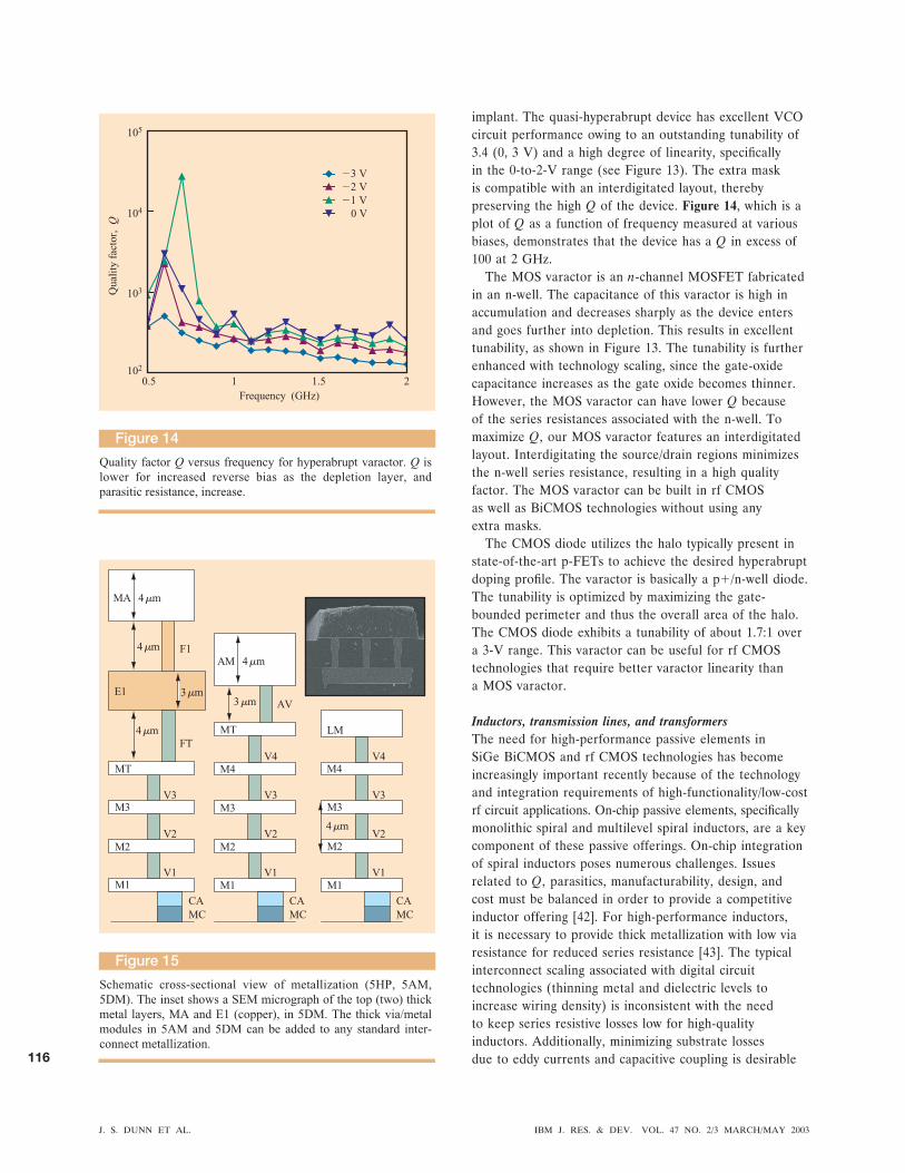
implant. The quasi-hyperabrupt device has excellent VCOcircuit performance owing to an outstanding tunability of3.4 (0, 3 V) and a high degree of linearity, specificallyin the 0-to-2-V range (see Figure 13). The extra maskis compatible with an interdigitated layout, therebypreserving the high Q of the device. Figure 14, which is aplot of Q as a function of frequency measured at variousbiases, demonstrates that the device has a Q in excess of100 at 2 GHz.
The MOS varactor is an n-channel MOSFET fabricatedin an n-well. The capacitance of this varactor is high inaccumulation and decreases sharply as the device entersand goes further into depletion. This results in excellenttunability, as shown in Figure 13. The tunability is furtherenhanced with technology scaling, since the gate-oxidecapacitance increases as the gate oxide becomes thinner.However, the MOS varactor can have lower Q becauseof the series resistances associated with the n-well. Tomaximize Q, our MOS varactor features an interdigitatedlayout. Interdigitating the source/drain regions minimizesthe n-well series resistance, resulting in a high qualityfactor. The MOS varactor can be built in rf CMOSas well as BiCMOS technologies without using anyextra masks.
The CMOS diode utilizes the halo typically present instate-of-the-art p-FETs to achieve the desired hyperabruptdoping profile. The varactor is basically a p�/n-well diode.The tunability is optimized by maximizing the gate-bounded perimeter and thus the overall area of the halo.The CMOS diode exhibits a tunability of about 1.7:1 overa 3-V range. This varactor can be useful for rf CMOStechnologies that require better varactor linearity thana MOS varactor.
Inductors, transmission lines, and transformersThe need for high-performance passive elements inSiGe BiCMOS and rf CMOS technologies has becomeincreasingly important recently because of the technologyand integration requirements of high-functionality/low-costrf circuit applications. On-chip passive elements, specificallymonolithic spiral and multilevel spiral inductors, are a keycomponent of these passive offerings. On-chip integrationof spiral inductors poses numerous challenges. Issuesrelated to Q, parasitics, manufacturability, design, andcost must be balanced in order to provide a competitiveinductor offering [42]. For high-performance inductors,it is necessary to provide thick metallization with low viaresistance for reduced series resistance [43]. The typicalinterconnect scaling associated with digital circuittechnologies (thinning metal and dielectric levels toincrease wiring density) is inconsistent with the needto keep series resistive losses low for high-qualityinductors. Additionally, minimizing substrate lossesdue to eddy currents and capacitive coupling is desirable
Figure 14
Quality factor Q versus frequency for hyperabrupt varactor. Q is
lower for increased reverse bias as the depletion layer, and
parasitic resistance, increase.
0.5 1 1.5 2
Frequency (GHz)
105
104
103
102
Quali
ty f
acto
r,
Q
�3 V
�2 V
�1 V
0 V
Figure 15
Schematic cross-sectional view of metallization (5HP, 5AM,
5DM). The inset shows a SEM micrograph of the top (two) thick
metal layers, MA and E1 (copper), in 5DM. The thick via/metal
modules in 5AM and 5DM can be added to any standard inter-
connect metallization.
CA
MC
M1
V1
M2
V2
M3
V3
MT
FT
E1
F1
MA
CA
MC
M1
V1
M2
V2
M3
V3
MT
CA
MC
M1
V1
M2
V2
M3
V3
M4
V4
AV
AM
M4
V4
LM4 m �
4 m �
4 m �
4 m �
4 m �
3 m �3 m �
J. S. DUNN ET AL. IBM J. RES. & DEV. VOL. 47 NO. 2/3 MARCH/MAY 2003
116

in order to increase Q. Integrating the inductors in thelast, thick metal levels of the BEOL and using largevias to provide a thick dielectric between the inductorand substrate helps reduce these effects [44].
Three basic metallization options are provided forspiral inductors in the IBM SiGe BiCMOS and rf CMOStechnologies: a 2-�m-thick aluminum level, a 4-�m-thickaluminum level, and a dual-metal stack of 4 �m aluminumand 3 �m copper. Figure 15 shows the integration of theselevels in the BEOL. These inductor offerings have evolvedover the last five years to provide high-performanceinductors as rf circuit function and integration needs haveevolved. Initially, the SiGe 5HP BiCMOS technology wasqualified in 1998 with 2 �m Al as the last metal [45]. Ascan be seen from Table 7, this aluminum layer has arelatively high sheet resistance (14 m�/�); therefore, apeak Q for a 1-nH inductor at 2– 4 GHz is in the rangeof 5 to 9. The need for higher-Q inductors drove thequalification of SiGe 5AM, an upgrade to the 5HP processwith a 4-�m Al layer for improved inductor performance[2]. This layout has a 4-�m-high via below it to allow foran additional thick interlayer dielectric (ILD) between theinductor and substrate. For a 1-nH inductor, a peak Q of18 can be realized with the 4-�m Al inductors in SiGe5AM at a frequency of about 5 GHz. The underpass, an0.8-�m-thick aluminum layer, has a high sheet resistancerelative to the thick aluminum layer. This fixed underpassresistance shows up in series with the relatively lowresistance of the 4-�m aluminum spiral metallization,limiting the achievable peak Q.
The latest IBM SiGe offering includes an additionaltwo thick, low-resistivity metal levels above the standardBEOL stack (“dual metal”). This stack was qualified forproduction in November 2001. The uppermost level isthick aluminum compatible with wire bonding or C4interconnections, with a second thick level composed ofcopper. Each of these levels has an additional 4 �m ofoxide below it to increase the dielectric spacing from levelto level and between the two levels and the substrate (seeFigure 15). This high-performance offering allows not onlyhigh-Q inductors (achieved by paralleling the two thickmetals for extremely low series resistance), but also highinductance density (achieved by connecting a spiral fromthe thick aluminum level in series with a spiral stackedbelow it on the thick copper level). The dual-metalinductor shown in Figure 16 has a peak Q of 28 over avery large frequency range. Efficiently coupled structuressuch as transformers (impedance matching and powersplitting) and baluns (balanced– unbalanced transformersused to convert differential signals to/from single-endedsignals and achieved by vertically stacking windings) arealso possible, with a 1:1 balun achieving a 3.5-dB untunedinsertion loss. In addition to the two thick levels, anoptional polysilicon shield is offered that can increase the
peak Q by as much as 30% for certain geometry spiralsin addition to reducing substrate noise coupling fromthe spiral.
The high-quality inductors achievable with the IBMdual-metal technology enable designers to integrate high-Q resonant circuits in support of low-phase-noise VCOs,narrow-band filters, low-loss-impedance matching, etc.The added ability to achieve high-quality integratedmagnetically coupled structures permits the realizationof on-chip baluns and transformers. Another uniqueadvantage of using two thick metal levels with a largeseparation distance is the ability to create nearly idealmicrostrip and/or coplanar waveguide (CPW) transmissionlines with very low loss. Typical CMOS/BiCMOS/SiGetechnologies are not able to achieve low-loss, idealtransmission lines because of the excessive series lossesand high capacitive coupling inherent in CMOSmetallization schemes.
ESD protection devicesElectrostatic discharge (ESD) protection of rf productsbecomes important as application frequencies exceed 1 GHz.At application frequencies below 1 GHz, the abilityto simultaneously achieve excellent ESD protection and
Figure 16
Plot of Q vs. frequency for a 1.1-nH dual-metal inductor. Re-
produced with permission from [41]; © 2002 IEEE.
10�1 100
Q
101 102
0
5
10
15
20
25
30
Frequency (GHz)
Table 7 Metal options available for fabricating high-quality passives such as inductors or transmission lines.
Metal Sheet resistance(m�/�)
Peak Q–1 nH/2– 4 GHz
2 �m Al 14 5–94 �m Al 7 184 �m Al/3 �m Cu 3.2 28
IBM J. RES. & DEV. VOL. 47 NO. 2/3 MARCH/MAY 2003 J. S. DUNN ET AL.
117

performance objectives was possible in most CMOS,BiCMOS, and SOI applications. As semiconductorapplications extend beyond 1 GHz, providing ESDprotection while simultaneously satisfying performancegoals, such as low capacitance on I/O pads, will increasein difficulty.
RF CMOS can utilize some of the traditional ESDsolutions that are common in the industry, although manyESD solutions are unacceptable because they precludelow capacitance, high Q, and low noise. MOSFETs havesignificant 1/f noise and capacitance loading, makingdiode-based and diode-configured ESD implementationsthe preferred solutions for rf applications [46]. Theintegration of shallow-trench isolation (STI) has allowedfor both optimization and scaling of the STI-bound p�/n-well diode, the STI-bound n�/substrate diode, and n-well-to-substrate diode structures from 0.5-�m to 0.1-�mCMOS technologies [46 – 49]. To maintain a constant ESDrobustness in order to counter the impact of dimensionalscaling from MOSFET constant electric field scalingtheory, constant ESD scaling theory indicates that ESDrobustness can be preserved by increasing the n-wellretrograde dose with successive technology generations[46]. With the introduction of the high retrograde welldose, the p�/n-well diode capacitance can be maintainedby adjustment of the n-well implant energy [46 – 49]. For rftechnologies, the introduction of low-doped p-substratesallows for lower n�/substrate and n-well-to-substratediode capacitance, as well as noise isolation of the ESDelements on adjacent circuitry [50 –53]. RC-discriminatornetworks, whose RC time constant is tuned to the ESDpulse rise time, are also utilized for triggering largeMOSFETs located between power supplies.
RF BiCMOS SiGe technologies offer even moreopportunity to introduce low-capacitance, high-Q, low-resistance robust ESD elements for ESD protection of rfcircuitry. First, for mixed-signal chips that contain digital,analog, and rf circuitry, different ESD solutions canbe applied to different functional circuit blocks. Theaforementioned CMOS ESD diode elements and RC-triggered MOSFET ESD power clamps can be utilized forthe digital functional block. Additionally, with the myriadof additional elements offered by BiCMOS technology,new ESD elements and circuits can be utilized to provideESD protection of digital, analog, or rf networks. This ispossible by taking advantage of the SiGe library elementsand the SiGe npn base, subcollector, and isolationstructures. SiGe passive elements such as SiGe varactorsand SiGe Schottky diodes, as well as active SiGe HBTnpn devices and SiGe HBT pnp transistors, can be utilizedin either diodic or bipolar configurations for networks[54 –58]. Low-capacitance emitter– base and base– collectorjunctions provide well-controlled high-Q junctions forESD protection networks. Low diode anode series
resistance is achievable in SiGe heterojunction bipolartransistor devices because of the high base dopingconcentration utilized in heterojunction transistors.Heterojunctions decouple the emitter– base junctioncapacitance from the base doping concentration designpoint. For ESD structures, this allows for improvedcurrent uniformity in multi-finger base– collector diodestructures. Additionally, low diode series cathoderesistance, significantly lower than the CMOS well designpoint, is achieved using the heavily doped subcollector,reach-through, and collector implants. Additionally,removal of the Kirk-effect limiting pedestal implantlowers base– collector junction capacitance for usageof SiGe varactors in the forward-bias mode with noESD robustness degradation. Deep-trench isolationalso provides for the use of deep-trench (DT)-boundsubcollector–substrate, DT-bound n-well-to-substrate,and DT-bound p�/n-well diode elements. The DT-boundstructures can provide low capacitance, improved latchupimmunity, and noise injection reduction, as well as higherdensity.
BiCMOS SiGe technology also allows for theintroduction of scalable ESD power clamps for analogand rf functional blocks. To provide an ESD solution thatnaturally scales with the BiCMOS technology and utilizesthe limitation of bipolar transistors, ESD power clampswere designed which take advantage of the Johnson limitof SiGe HBT devices [59 – 61]. The Johnson limit can besimply explained as the product of the breakdown voltageand cutoff frequency of a transistor being a constant,V*
m fT � const. Thus, fT can be traded off againstbreakdown voltage.
Hence, from the Johnson limit, V*m f*T is associated with
a first transistor, and Vm fT is associated with a secondtransistor. The ratio of breakdown voltages can bedetermined as (V*
m/Vm) � ( fT/f*T) . Using this Johnsonrelationship, an ESD power clamp can be synthesized inwhich a trigger device with the lowest breakdown voltagecan be created by using the transistor with the highestcutoff frequency ( fT), and a clamp device with the highestbreakdown device will have the lowest cutoff frequency.Figure 17(a) shows an example of a Darlington-configuredbipolar power clamp with a 47-GHz/4-V BVCEO triggerdevice that supplies the 27-GHz/6-V BVCEO clamp device.A 7-� ballast resistor was used for each leg of the clampdevice. A 7-k� bias resistor was used below the triggerdevice to limit the current. In this power clamp, thetrigger device had an open base configuration, allowingearly breakdown of the trigger circuit. Figure 17(b) showsthe human body model (HBM) ESD results. In a givenBiCMOS SiGe technology, a large number of SiGe HBTswith different breakdown voltages are available toestablish different trigger conditions for applicationswith different power supplies.
J. S. DUNN ET AL. IBM J. RES. & DEV. VOL. 47 NO. 2/3 MARCH/MAY 2003
118

There are many advantages of the BiCMOS SiGe ESDclamp compared to RC-triggered MOSFET ESD powerclamps. First, SiGe ESD power clamps provide a muchhigher robustness per unit micron. The RC-triggeredMOSFET ESD power clamp achieves less than 2.5 V/�m,while the SiGe HBT npn achieves 15–30 V/�m of npnwidth. Second, the BiCMOS SiGe ESD clamp canbe used for negative-power-supply voltage products. Adisadvantage of the MOSFET RC-triggered clamp in asingle- or dual-well technology is that it cannot be usedbetween VDD and negative-power-supply VEE because ofMOSFET overstress. Third, in contrast to MOSFET ESDnetworks, the ESD robustness per unit micron (width)does not decrease with successive rf technologygenerations. Experimental results from three successiveSiGe technologies do not show degradation of ESDrobustness.
To evaluate the ESD scaling of a SiGe HBT device, adimensionless group can be established explaining therelationships among thermal conduction, thermal capacity,failure temperature, pulse width, saturation velocity,maximum electric field condition, and the unity currentgain cutoff frequency [52, 62– 64]. This analysis shows thatthe frequency of the SiGe HBT increases as the maximumpower decreases. As the device dimensions are scaled toachieve these objectives, the power at which failure occurswill decrease unless doping and material changes areaddressed. To produce future high-fT devices, dimensionalscaling, doping concentration, and material changes will beneeded. This will entail optimization of concentrations ofthe base dopant, Ge, and carbon. In the evolution of theseHBT devices, the choices made to achieve the BVCEO andthe fT will influence both the maximum power and ESDrobustness.
3. Communications technology design andprocess development
Technology designAlthough Si/SiGe HBT devices have been proposed formany years, the first practical SiGe devices were fabricatedin IBM in the late 1980s, in large part enabled by thedevelopment of the ability to grow Si/Ge epitaxial layersat low temperatures using ultrahigh-vacuum chemicalvapor deposition (UHV/CVD) [65]. This technique freeddevice designers to be able to grow arbitrary dopingprofiles without the constraints of high thermal cyclespreviously thought necessary for the creation of perfectlycrystalline material. This activity has led to substantialimprovements in the SiGe HBT over several generationsby careful scaling of the epitaxial transistor (ETX) device[66] with changes in the low-temperature epitaxy (LTE)base region through modifications in Ge ramp, boronprofile, collector design, and carbon doping.
Decisions for the development of new technologies areinitiated by marketplace and circuit design requirements,which in turn determine the choice of a BiCMOStechnology. While HBT performance ( fT, fmax, and IC
at peak fT) is frequently of prime importance for thesedecisions, attention must be paid to CMOS generation(performance, density, VCC, ASIC compatibility), passiveelements, and current-carrying capability. Furtherrestrictions may be placed on a technology by cost andreliability needs. These technology requirements aregenerated primarily by the marketplace and individualcustomer strategy. The IBM technology designmethodology has been to drive continuous improvement inperformance of HBT, CMOS, interconnection technology,and passive elements. Exploitation of all of theseenhancements simultaneously, generally introduced intothe IBM SiGe high-performance (HP) technologies,increases process complexity and mask count and,therefore, cost. While this is necessary for a large segmentof the BiCMOS marketplace, smaller individual marketscan be satisfied with reduced technology features throughcareful development of analog derivative technologies ata reduced cost.
Figure 17
(a) SiGe HBT ESD power clamp utilizing a high-fT/ low-BV
CEO
trigger element and a low-fT/high-BV
CEO clamp element. The
ballast and bias resistors are 7 � and 7 k�, respectively. (b)
Human body model (HBM) ESD robustness as a function of SiGe
HBT power clamp emitter width. Reproduced with permission
from [59]; © 2001 IEEE.
Trigger device
VDD
VSS
Rbias
Rballast
10000
8000
6000
4000
2000
0
HB
M E
SD
level
(V
)
0 200 400 600
SiGe npn emitter width ( m)
(b)
(a)
�
Clamp device
IBM J. RES. & DEV. VOL. 47 NO. 2/3 MARCH/MAY 2003 J. S. DUNN ET AL.
119

With improvements in both CMOS performance andpassive elements, a major market for rf CMOS is alsoemerging, with new issues which must be addressed.Smaller chip sizes, a pad-limited total chip area, and thepredominance of passive components are layout issuesthat generally distinguish analog and rf designs from theirdigital counterparts. At the same time, passive device areaand wire-bond pads have not decreased with the reducedlithography dimensions; chip areas remain roughly thesame for a given function, even with improved lithographydimensions. Consequently, the economic forces drivingreduced lithography in digital CMOS technologies (thatis, the tradeoff between the lithography-driven chip costincrease and the ability to obtain more chips on a wafer ormore functionality per chip) do not apply in the analogand rf domain.
Digital CMOS trends do not influence analog designs.They are costly, and in many cases digital CMOS changesmake analog designs significantly more difficult. Forexample, metallization trends toward thinner films resultin higher inter- and intra-level capacitance (per unit area),thereby compromising the performance of designs thatretain device-to-device distances between technologygenerations. These manufacturing limitations are inaddition to analog circuit requirements that make it moredifficult to design with reduced supply voltages. The netresult from this “nonscaling” is that, when compared todigital CMOS, analog and rf technology roadmaps are lessdefined. Market and targeted design understanding arecritical to defining the best mix of technology elementsand dimensions.
Process integrationIBM has demonstrated leadership in the developmentof world-class analog bipolar and BiCMOS processtechnologies since its introduction of the world’s first SiGebipolar technology, SiGe 5E, into production in 1996 [67].Although this premier technology, intended for earlyfabrication of wireless circuits, did not include all CMOSelements, subsequent high-performance (SiGe HP)technologies have all been fully compatible withcorresponding ASIC CMOS technology, resulting inthe ability to integrate large amounts of both high-performance analog and digital signal processing. Theevolution of these SiGe production technologies spanning0.5-�m, 0.25-�m, and 0.18-�m generations has beenthrough a combination of vertical scaling (improved SiGeepitaxial films and bipolar profiles), horizontal scaling(improved lithography dimensions and overlay), andCMOS innovation (gate lengths, density, and metallizationtechnology). The improvements in SiGe HP technologyare illustrated in Figure 21 (shown later). Details of thesetechnologies demonstrate that the primary technologicaldriver in going from SiGe 5HP [68] to 6HP [2] was
improvement in CMOS, while the migration to 7HP[3] was driven by bipolar performance and includedthe addition of Cu BEOL and further substantialimprovements in CMOS.
Semiconductor innovations have been introducedinto each successive technology in order to meet therequirements of the marketplace for the rapidly growingwireless industry and the need for higher-bandwidthoptical networking products. The development of anintegrated SiGe BiCMOS technology originates with anunderstanding of semiconductor requirements imposed bythe marketplace. The wireless customer envisioned forSiGe 5HP could be serviced with a cost-competitiveCMOS technology (ASIC CMOS 5X) and analogcapabilities achieved with a 50-GHz HBT capable ofdriving speeds for applications in the 2–5-GHz range.HBT and CMOS technologies were successfully mergedby sharing a common polysilicon film for both bipolarextrinsic base and CMOS gate structures. This integrationmethod, referred to as base-during-gate (Figure 18),allowed cost-efficient use of films and masking levels andwas made possible by the thermal compatibility of earlyCMOS structures with the rather deep emitter profiledeveloped in the early HBT. It was clear that Ge dopingprofiles had a profound effect on both HBT performanceand strain that could result in decreased circuit yields,so Ge doping was intentionally kept low to facilitateearly production learning. Acceptability by the analogmarketplace also required the addition of the high-qualitypassive elements (resistors, capacitors, inductors, etc.)discussed in detail in the preceding section.
SiGe 6HP was developed first for applications used instorage products which require a very large circuit countof high-performance CMOS such as the read-channel chipdescribed in the next section. For these applications, itwas necessary to replace the 0.5-�m CMOS of SiGe 5HPwith the 0.25-�m CMOS 6SF. The reduced thermalcycle used in this CMOS generation also required amodification of the integration from base-during-gate toan integration methodology, which fabricated the criticalemitter– base region of the HBT after CMOS structureswere in place [Figure 18(b)]. While this integrationrequires careful protection of the CMOS gate conductorduring the processing of the HBT, and subsequentremoval of these protective films, this base-after-gateintegration was successful in the decoupling of thermalcycles required for narrow HBT profiles and the CMOSdevice activation.
While the first two generations of SiGe BiCMOS couldsuccessfully service applications up to 10 Gb/s (OC-192SONET), 40-Gb/s (OC-768) optical networking productsrequire a substantially faster bipolar transistor. SiGe7HP was developed for this high-switching-speed-drivenapplication space. Since designers request bipolar devices
J. S. DUNN ET AL. IBM J. RES. & DEV. VOL. 47 NO. 2/3 MARCH/MAY 2003
120

that switch at approximately three times the bit rate ofmultiplexing and demultiplexing circuits, the SiGe 7HPtarget was established at a maximum oscillation frequencyof 120 GHz. To successfully achieve these speeds,previously widely believed to be achievable only withIII–V compound semiconductors (notably InP-basedHBTs), vertical scaling (reduction of epi base andcollector profiles) as well as horizontal scaling of the HBTdevice was necessary. The reduction of vertical profilesnecessitated careful control of process thermal cycles aswell as the use of carbon doping [69], which had not beennecessary in the early generations of IBM SiGe BiCMOS.In addition to continued improvements in passives,the integration of this technology with CMOS 7SF(0.18-�m gate length) marked the introduction of Cuinterconnection technology, which further enhanced thecurrent-carrying capability of high-performance circuits.
The self-aligned HBT transistor utilized in generations5HP, 6HP, and 7HP required evolutionary modificationsof the ETX transistor [66], which featured the ionimplantation of the heavily doped extrinsic base regionof the device. Further scaling of the ETX device wouldrequire extensive reduction in intrinsic base doping. Thiswould lead to high pinch base sheet resistance, whichwould lead to a non-optimal design point for a technologybased on high manufacturability. Necessary improvementsto ETX in base resistance (and collector–base capacitance),which determined the maximum available power gainfrequency, fmax, were limited by this device structure.This shortcoming therefore led to the development ofa new integration scheme. The raised extrinsic base(RXB) bipolar was introduced to allow further verticaland horizontal scaling without the limitations imposedby the ETX device. By contacting the lightly dopedintrinsic base with an additional boron-doped polysiliconfilm, these constraints were lifted, and the HBT introducedfor SiGe 8HP integration has demonstrated fT and fmax
values in excess of 200 GHz. 5
In addition to the flagship 5HP, 6HP, and 7HP SiGetechnologies, several derivative SiGe technologies havebeen developed to capture smaller markets with morespecific requirements. These derivative technologiesinclude SiGe 5PA, SiGe 5MR, and BiCMOS 5HPE, whichare targeted respectively at rf power amplifier, disk drivepreamplifier, and wireless applications.
The SiGe 5PA technology was developed as a derivativeof the SiGe 5HP technology targeted at the rf poweramplifier market. Power amplifiers for wireless handsetshave historically been built using GaAs because of its abilityto achieve the competing breakdown and linearityrequirements that were previously unattainable withsilicon technologies. SiGe 5PA meets these requirements
5 B. Jagannathan, unpublished communication.
Figure 18
Schematic process flow diagram for (a) 0.5- m base-during-gate
(BDGate) production technology. (b) 0.25- m and 0.18- m base-
after-gate (BAGate) production technology. Note the reduced
number of analog and bipolar blocks compared to the BDGate
process, because the CMOS now contains many analog modules.
(For both cases, the CMOS backbone represents the base CMOS
process. Insertion points are shown for analog and bipolar
process modules.) Reproduced with permission from [2] and
[44]; © 1999 and 2001 IEEE.
n+ subcollector,
n-epi, deep-trench
isolationShallow trench
Reachthrough to n+
subcollector, bipolar
protect layer
Bipolar window
(BW), SiGe base
deposition, self-
aligned extrinsic
base I/I, emitter
definition and
opening, collector
implant, n+
polysilicon emitter,
extrinsic base
pattern and etch
p-FET S/D/G I/I, final
RTA, resistor salicide block
mask, salicide and contacts
Standard interconnect
technology including MIM
capacitor
FET well and VT implants,
gate oxidation, polysilicon
gate deposition, pattern,
and etch, polysilicon
reoxidation, FET
extensions, sidewall
formation, n-FET S/D/G
I/I, FET protect deposition
Analog element BipolarCMOS backbone
Analog element Bipolar
Shallow-trench isolation
Gate oxide, polysilicon
deposition
Polysilicon gate and
extrinsic base etch, gate
reoxidation, FET
extensions, spacer deposit
Spacer etch, FET source/
drain/gate (S/D/G) I/I,
final anneal
Salicide and contacts
Interconnect technology
FET well/VT implants
CMOS backbone
Resistor
salicide
block mask
Metal-
insulator-
metal (MIM)
capacitor
Precision
capacitor
Ion-implanted
resistor
Subcollector, n-epi,
deep trench
Reachthrough to n+
subcollector
Bipolar window,
SiGe base
deposition, self-
aligned extrinsic
base ion implant
(I/I), emitter
definition and
opening, collector
implant, n+
polysilicon emitter
formation
(a)
(b)
�� �
IBM J. RES. & DEV. VOL. 47 NO. 2/3 MARCH/MAY 2003 J. S. DUNN ET AL.
121

with a high-breakdown SiGe HBT that has a BVCEO of 7 Vand a BVCBO of 20 V. The increased breakdown voltagesare achieved, while minimizing the impact to the devicelinearity and fT, through modification and optimization ofthe collector doping profile. The technology is definedsuch that the remaining device set is common with thosein the parent SiGe 5HP technology.
The SiGe 5MR technology was developed for diskdrive preamplifier applications, which have a conflictingcombination of performance and voltage technologyrequirements between the read and write portions of thechips. The read-amplifier portion of the chip must amplifyextremely small signals from the magnetoresistive read
element while not significantly degrading the signal-to-noise ratio (SNR). Conversely, the write portion of thechip requires high-voltage devices to drive high-speedsignals through the inductive write head. The SiGe 5MRtechnology includes a SiGe HBT capable of achieving theperformance and noise requirements of the read amplifier,yet having a BVCEO of 10 V to support the voltagerequirements of driving the inductive write head. TheCMOS devices included in the technology for logic controlcircuitry support the industry-standard disk drive supplyvoltage of 5 V. The technology was developed bycombining the 5-V CMOS devices from CMOS 5SF, theproven SiGe HBT from SiGe 5HP, breakdown voltageenhancements similar to SiGe 5PA, and the base-after-gate integration scheme from BiCMOS 6HP. Additionaldevelopment efforts focused on adding features suchas a lateral pnp, an isolated n-FET, and a polysilicon–polysilicon capacitor, as well as process simplificationstargeted at cost and cycle-time reduction.
These features of the SiGe 5MR technology are all keyelements included in its derivative technology, BiCMOS5HPE [70]. The combination of a rich feature set andsimplified process provided by this technology makes itwell suited for the competitive wireless marketplace. TheBiCMOS 5HPE technology includes the features of SiGe5MR, together with an additional higher-performanceSiGe HBT and enhanced passives such as the 1.35-fF/�m2
MIM, high-Q inductors, and MOS varactor. Processsimplifications such as replacing long furnace anneals withrapid thermal anneals (RTAs) significantly reduce theproduction cycle time. This cycle-time reduction is extremelyvaluable for wireless product developers who depend onmultiple design passes to debug sensitive rf circuits.
Manufacturing issuesTo introduce semiconductor technology into a productionenvironment, it is necessary to demonstrate a rigorous setof manufacturability standards. These requirements canbe loosely categorized as repeatability, reliability, andyield. Device models are developed to describe devicesfabricated using a large statistical database collectedon a substantial quantity (typically 100 –300) of wafersfabricated during this assessment. These models begin byanalysis of device parameters, as illustrated in Figure 19.The models describe nominal values and distributions ofmanufactured devices from probability plots. Similardata is collected on in-line measurements of physicalparameters such as lithographic critical dimensions andoverlay, film thicknesses, and layer resistances and physicalproperties. Both device electrical data measured on teststructures and in-line parametric measurements arecollected during the qualification in order to demonstratestatistical process control (SPC) [71]. SPC methodscompare measured data to well-defined process
Figure 19
Example of statistical device models showing (a) histogram of
VBE
for 0.5- m � 1.0 m HBT at 10 A emitter current; (b)
probability plot for VBE
comparing measured hardware
(diamonds) on approximately 2000 samples and device model
(circles) to a normal distribution (curve). Reproduced with per-
mission from [45]; © 1997 IEEE.
0.77 0.78 0.79 0.8 0.81�3
�2
�1
0
1
2
3
�0.85 �0.8 �0.75 �0.7 �0.650
200
400
600
800
1000
1200
1400
VBE
(V)
(a)
VBE
(V)
(b)
Quanti
ty
� � �
J. S. DUNN ET AL. IBM J. RES. & DEV. VOL. 47 NO. 2/3 MARCH/MAY 2003
122

specifications and must meet rigorous standards in orderto proceed with volume production. SPC measurementsof Cp (a gauge of process centering) and Cpk (processcapability index) are illustrated in Figure 20. A Cpk valueof 1.0 represents the point at which 3 of the populationdistribution is within the specified manufacturing controllimits, with values in excess of 1.0 indicative of muchtighter production control.
SiGe HBT reliability stressing is conducted in bothforward-bias and reverse-bias modes, using the sameaccelerating stress conditions and analysis techniquesdeveloped for previous implanted-base silicon bipolartechnologies [72]. In forward bias, less than 5% changein npn current gain � over a 500-hour stress at 140 Cand 1.3 mA/�m2 (near peak fT) was found for the 0.5-�m-generation SiGe HBTs. Most GaAs HBT technologies arestressed at currents far less than their peak fT current [73],which does not represent realistic use conditions. Usingempirically determined acceleration factors, the SiGeHBT forward-bias result is equivalent to less than 10% �
degradation under typical-use conditions (1.25 mA/�m2 at100 C) after 100 000 power-on-hours (POH). Change in �
has been attributed to electromigration-induced pressureon the emitter contact, causing decreased collector currentwith stress condition [74]. Reliability at high currentdensities with SiGe 7HP and 8HP vertical scaling alsorequires a careful look at the choice of interconnectiontechnology and device self-heating considerations [75].With reverse bias of 2.0 V or less, no measurable changein base or collector currents is observed at a worst-casecondition of �40 C. Hot-electron degradation with reversebias stress is also typical of bipolar junction transistors andis substantially lower for the epitaxial (epi)-base deviceswhen compared to ion-implanted base double polysilicon [74].This result is attributed to the reduction of the electricfield at the emitter– base junction due to a base dopingsetback which can be achieved with epitaxial base growthand is expected to be similar with HBT vertical andhorizontal scaling.
A major focus for final production qualificationdecisions is the capability of a technology to achieve highmanufacturing yields. FET yield assessment and controlin SiGe BiCMOS technologies is adopted from the parentCMOS technologies, with an added focus on ensuring thatthe SiGe process steps do not degrade the FET yield. Forexample, with the base-after-gate integration scheme,several bipolar films are deposited over the FETs and thensubsequently etched away. Defect-free removal of thesefilms over the FET regions is critical to minimize yieldloss due to shorting. Successful removal of the bipolarfilms from the FET regions is monitored with both large-area defect monitors and CMOS SRAM yields. A BiCMOS6HP 30-lot yield trend for large-area monitor structures [2]demonstrates that BiCMOS yields are equivalent to the
typical yield of the parent CMOS technology. CMOS SRAMyields were also shown to be within the parent CMOS targetrange, as indicated by the BiCMOS 6HP CMOS SRAM yieldtrend shown in Figure 21.
Silicon bipolar transistor device yield has historicallybeen limited by dislocations in the silicon crystal thatcause junction shorting [76]. One would expect SiGeHBTs to have a higher density of these dislocationsbecause of defect formation during epi growth and strainin the Ge layer. However, the low-temperature epitaxy(LTE) process technology produces a relatively defect-freeepi layer and does not significantly contribute to yieldloss. Also, minimizing the post-epi growth during thermal
Figure 20
Statistical process control chart showing achievement of good
process control over a wide range of in-line process measure-
ments. Values of the process capability index (Cpk) of 1.0
indicate process measurements at the 3 control point. Values of
1.5 are considered under 6 control.
1 3 5 7 9 11 13 15 17 19 21 23 25 27 29
Measurement parameter
0
0.5
1.0
1.5
2.0
2.5
3.0
Cpk v
alu
e
Figure 21
Static RAM functional perfect (zero bit fails) yield data from a
154K RAM (12- m2 cell size, one million FETs) by wafer. Re-
produced with permission from [2]; © 1999 IEEE.
�
Wafers
100
80
60
40
20
0
Yie
ld (%
)
IBM J. RES. & DEV. VOL. 47 NO. 2/3 MARCH/MAY 2003 J. S. DUNN ET AL.
123

cycles helps reduce the possibility of forming defectsdue to the strained layer. The primary cause for defectgeneration has been found to be related to stress dueto shallow-trench isolation (STI). As a result, theSTI formation process has been optimized in order tominimize the stress and increase the HBT yield. Figure 22shows a SiGe 5HP 20-month all-good-yield trend of anarray of 4000 HBTs. Initially, the yield was depressed,averaging in the 60 –70% range. Through carefuloptimization of the HBT process, the yield has beenimproved substantially, to above 90% [77].
The real test for the success of a SiGe BiCMOStechnology was being able to design and manufacturehighly integrated products with good yields. An exampleof an integrated circuit that was produced in high volumeat the IBM Essex Junction facility is a read-channel chipthat translates analog signals from a disk-drive read headinto digital words. The analog data is interpreted using apartial response maximum likelihood (PRML) signalprocessing algorithm. The chip was clocked at a rate of75 MB/s, which was the fastest PRML chip speedpublished at that time.
4. Technology implications in design
Device noise and isolation issuesNoise plays a pivotal role in the design of both wirelessand wired communications systems. In a wireless system,for example, data is carried by a signal that resides over aspecified bandwidth and assigned frequency. In-band noiseadded to the signal by the transmitter circuits duringtravel through the free-air channel and noise within thecircuits of the receiver combine to decrease the SNR.Together with the available bandwidth, this SNR has a
direct impact on the data rate that the system can achievefor a given bit-error rate. While the SNR can be improvedby increasing the transmitted power or decreasing thetransmission distance, such strategies trade off directlyagainst the market trend for increased range, portability,and battery life. Noise is a key limiting factor in theperformance of optical networking systems as well,particularly with data rates now exceeding 40 Gb/s. Suchhigh rates compress each data symbol into an extremelysmall interval of time and require precise timing to detect.Any noise or jitter in this timing, such as from phase noisein the circuits that generate the clock signal, can result ina detection error.
Noise may be introduced into a signal in a variety ofways. One source is the set of devices, both active andpassive, comprising the circuits of the transmitter andreceiver chips. In a technology capable of system-levelintegration, however, noise may also be introduced whenone circuit injects an unwanted signal into another circuiton the same chip, either through the air or the substrate.Understanding each of these various noise properties isessential for the optimal design of low-power, high-data-rate communications chips. The IBM SiGe BiCMOStechnologies each feature a device library containing awide variety of bipolar, FET, and passive devices. Indeveloping a circuit, a designer selects one device overanother based on relative merits, including the expectednoise performance of a circuit employing that device.Several figures of merit are used, depending on the circuitapplication.
One of the most common circuits in analog and rfdesign is the amplifier. In a wireless receiver, for example,the signal present at the antenna is often very weak. Thissignal is first narrow-band filtered to eliminate all out-of-channel energy, including noise, before passing through alow-noise amplifier (LNA) designed to increase the signallevel significantly while introducing as little noise aspossible. In this class of circuits, the noise property ofgreatest interest is how the SNR of the narrow-band signalat the channel frequency is degraded from input to output.This property may be captured through a figure of meritknown as the noise figure, which is defined simply asthe input SNR divided by the output SNR at a giventemperature. The noise figure may be measured betweenthe input and output of an individual active device as well.An ideal, noise-free device displays a noise figure of 1 (or0 dB, as it is most commonly expressed), while the noisefigure of a physical device is higher. Since the noise figuredepends on the impedance of the input source, the deviceunder test is commonly measured over a variety of sourcetunings in order to find the state (typically stated asreflection coefficient, �opt) that achieves the minimumnoise figure value (Fmin). The power gain (GA) associatedwith this tuning state can be noted as well.
Figure 22
Example of yield learning showing HBT yield improvement over
time through modification of process controls. Copyright Canon
Communications LLC. Used by permission.
Month
0
10
20
30
40
50
60
70
80
90
100
Yie
ld (%
)
Non-optimized STI
Optimized STI
STI control improvements
J. S. DUNN ET AL. IBM J. RES. & DEV. VOL. 47 NO. 2/3 MARCH/MAY 2003
124

In a BiCMOS technology, designers have the optionof using bipolar or FET transistors as active devices inanalog and rf circuits. The SiGe bipolar device featuresseveral intrinsic properties that make it particularlyattractive for low-noise circuits such as LNAs. Theseproperties can be understood in terms of the simplifiedbipolar equivalent circuit noise model illustrated inFigure 23. The model focuses on the three sourcesof noise that dominate in a typical modern device.
The first source is thermal noise generated inproportion to the temperature and value of the baseresistance, RB, and the design of the SiGe bipolar achievesa low value for this resistance. Germanium narrows thebandgap of the base with respect to the emitter,decreasing the amount of hole injection into the emitterfor a given electron injection into the base. This effectcompensates for the loss of � that would otherwise occurwith high base doping, allowing a reduction in the sheetresistance of the intrinsic base. Further, the lateraldistance that base current must travel through the intrinsicbase from edge to center can be made quite small throughthe use of advanced lithography to define a very narrowemitter stripe width. Such a narrow width is made possibleby a polysilicon emitter construction that achieves uniformdopant distribution even at dimensions of 0.1 �m.
A second source of high-frequency noise in the bipolartransistor is the fundamental operation of the emitter–basep–n junction itself, which contributes shot noise inproportion to both the base (IB) and collector (IC)currents. The SiGe bipolar device keeps these noisecomponents under control by two means. The high �
created by the presence of Ge in the base keeps IB low forany given IC bias, reducing IB shot noise. Further, the lowparasitic resistances and capacitances that contribute tohigh fmax (e.g., RB and CCB) result in high power gain attypical frequencies of interest. This high gain allows aninput signal to be amplified to much larger levels beforethe addition of shot noise, reducing the impact of this shotnoise on the output SNR and thus improving the noisefigure.
Although these generic SiGe bipolar features favor alow noise figure for any given generation, there is also ageneration-to-generation scaling trend toward a lowernoise figure. This improvement results from distinct lateraland vertical scaling trends in device design. Lateral scalingreduces RB and improves gain by reducing parasiticcapacitances. Vertical scaling leads to reductions in transittime that further improve power gain. Both RB and gainmay also improve as a result of fundamental changesin device architecture aimed at reducing parasitics.
Figure 24(a) displays both the minimum noise figure, Fmin,and associated gain GA as a function of IC for a 0.5-�m-generation (45-GHz fT, 65-GHz fmax) device with anemitter area ( AE) of 40 �m2. The 0.5-�m technologies,
Figure 23
Simplified equivalent circuit noise model for a bipolar transistor.
B C
VB
2 IB
2 IC
2
CBE
CCB
RB
�IB
R�
Figure 24
Minimum noise figure and associated gain for a 0.5- m-genera-
tion SiGe bipolar transistor with an emitter area of 40 m2,
measured at 2, 5, and 10 GHz (VCB
� 1 V). (b) Minimum noise
figure and associated gain for an 0.18- m-generation SiGe bi-
polar transistor with an emitter area of 25.6 m2 measured at 3, 10,
and 20 GHz (VCE
� 1.5 V). Reproduced with permission from
[7]; © 2001 IEEE.
0 5 10 15 20 25 30 350.0
0.5
1.0
1.5
2.0
2.5
3.0
3.5
4.0
4.5
Fm
in (
dB
)
IC
(mA)
(a)
IC
(mA)
(b)
0
5
10
15
20
25
30
2 GHz
5
10
0 5 10 15 20 25 30 350.0
0.5
1.0
1.5
2.0
2.5
3.0
3.5
4.0
4.5
Fm
in (
dB
)
GA
(
dB
)G
A (
dB
)
0
5
10
15
20
25
30
3 GHz
10
20
AE � 40 m2
VCB
� 1 V
�
AE � 25.6 m2
VCE
� 1.5 V
�
��
��
IBM J. RES. & DEV. VOL. 47 NO. 2/3 MARCH/MAY 2003 J. S. DUNN ET AL.
125

including IBM SiGe 5HP and 5AM, are the generationsmost widely used at present for 1–5-GHz wirelesstelephony and data networking because of the attractivecost–performance balance. The figure shows data for twofrequency bands. At 2 GHz, near the band used by severalstandards of wireless telephony, we observe that thedevice achieves a minimum noise figure of 0.8 dB at acurrent of 1 mA. At the higher bias of 5 mA, the devicemaintains Fmin below 1 dB, with an increased associatedgain of 20 dB. At 5 GHz, a band used for high-bit-ratewireless data networking, Fmin remains below 1.5 dB, withan associated gain of 14.2 dB at the same 5-mA bias.While there are no high-volume wireless applicationsin the 10-GHz regime at the moment, we note that anIBM device shows Fmin of about 2.3 dB in this band, withassociated gains of 10 –12 dB. As we note below, a 40-�m2
device area is non-optimal for 10-GHz operation owing tosource-matching difficulties. Indeed, smaller devices (e.g.,AE � 2.5 �m2) have demonstrated 10-GHz Fmin values of�1.8 dB.
High-frequency noise performance improves on movingto the 0.25-�m SiGe BiCMOS generation (e.g., 6HP).While the basic structure of the 0.25-�m bipolar is similarto that of the 0.5-�m generation, the lithographicimprovements allow for a somewhat narrower emitterstripe, achieving a reduced RB. The result is an improvementin Fmin of about 0.1 dB in the 1–10-GHz span. Combinedwith the ability to integrate a more aggressive CMOS,this generation is also attractive for use in the 1–5-GHzband, while adding the ability to mix analog/rf circuitswith large gate counts of high-speed logic.
Both the 0.5-�m and 0.25-�m SiGe generations offer ahigh-breakdown voltage variant of the bipolar transistor,featuring a modified collector profile that also results inreduced RB and CCB. Although this transistor suffersfT falloff from the Kirk effect at much lower currentdensities compared with the high-fT variant, this currentthreshold is much higher than the biases resulting in bestnoise performance and is thus not a limitation. A designercan achieve an additional improvement in Fmin of about0.1 dB by using this device, although the poorer linearitycharacteristics of the device may limit suitability for manyapplications.
Although the first applications of the 0.18-�m-generation SiGe BiCMOS technology, known as 7HP,have been 40-Gb/s optical networking, the technology alsorepresents a significant improvement in noise performanceand may therefore be attractive for wireless design as well.The benefits result from both lateral and vertical scaling,which improve RB, �, and power gain in the device. Theimprovements in gain are particularly important forreducing the noise figure at higher frequencies (e.g.,10 GHz and above). As an example, Figure 24(b)illustrates Fmin and GA behavior vs. IC for a 25.6-�m2
device at 3, 10, and 20 GHz. The 3-GHz band is closeto the unlicensed 2.4-GHz band commonly used forwireless data networking. At this frequency, the 7HPdevice achieves an Fmin value of only 0.4 dB andmaintains this value for associated gains exceeding 20 dB.At 10 GHz, Fmin climbs to only 0.6 dB, demonstrating thepossibly greater suitability of the 0.18-�m generation forhigher-frequency wireless work compared to 0.5 �m and0.25 �m. Associated gains exceed 12 dB. Further, Fmin
values of 1.7 dB are achievable out to 20 GHz,approximately double the frequency of the earliergenerations for equivalent performance and consistentwith the 2.5� (1.5�) increase in fT ( fmax).
Tuning for a desired combination of noise figure andassociated gain requires a designer to create a networkto match the source impedance (typically 50 �) to theoptimum noise impedance of the device. This task isgreatly simplified if the real part of the desired match isalready 50 �, allowing the imaginary part to be matchedwith a simple inductor in series with the base. Thiscondition may be realized by scaling the device areaappropriately. For example, for a 0.5-�m-generation,40-�m2 bipolar transistor biased at an IC of 5 mA,Fmin at 2 GHz is achieved at a matching impedance of(68 � j37) �. Scaling the device up to the slightly largerarea of 54 �m2 would achieve the desired 50-� real match,requiring an approximately 3-nH series inductor to completeto match. In comparison, a 0.18-�m-generation, 25.6-�m2
bipolar biased at 10 mA achieves an optimal match at10 GHz with a source impedance of (7.7 � j13.6) �,pointing out the need to scale the device down to amore suitable emitter area of 3.9 �m2.
High-frequency, or broadband, noise is not the onlycategory of noise pertinent to analog and rf design. Inaddition to low-defect-density single-crystal silicon, thestructures of both bipolar and FET transistors contain anumber of interfaces to surface films, particularly to SiO2.These interfaces contain a relatively large number ofdefects which act as electron and hole traps. The exchangeof carriers between these traps and the active regions ofthe device leads to the phenomenon of 1/f noise. Thismechanism manifests as a high noise energy content neardc, tapering off with frequency approximately as (1/f )n
before merging with the broadband noise spectrum at ahigher frequency approximated by a figure of merit knownas the corner frequency. As initially introduced into thesignal by the device, this low-frequency noise is generallyout of band. However, subsequent signal processing by amixer can shift the noise spectrum to straddle the carrierfrequency, potentially causing jitter as well as interferingwith adjacent channels. Thus, designers will seek adevice with good 1/f noise properties when creatingcircuits such as LNAs and VCOs that eventually sendtheir output to a mixer.
J. S. DUNN ET AL. IBM J. RES. & DEV. VOL. 47 NO. 2/3 MARCH/MAY 2003
126

Bipolar and FET devices differ greatly in their 1/fnoise properties. Because the electrical characteristics ofthe bipolar transistor are determined by mechanismsthat occur below the surface of a silicon substrate,away from oxide interfaces, these devices showsignificantly better 1/f noise results than FETs.Indeed, generation-to-generation scaling in FETsmoves oxide interfaces even closer to the activechannel, resulting in worsening of 1/f performance.The bipolar device is largely immune from this,maintaining a low corner frequency across generations.
Figure 25 compares the 1/f performance of four devicesfrom the 0.18-�m SiGe 7HP BiCMOS technology: a 3.3-Vn-FET, a 3.3-V p-FET, a high-fT SiGe bipolar, and a high-breakdown SiGe bipolar. We focus on the 3.3-V FETvariants here, since these devices support the highersupply voltages commonly used to achieve signalheadroom6 in analog circuit design. The proximityof surfaces contributes significant noise signal inthe n-FET, extending out well beyond 100 kHz. Thep-FET is an order of magnitude better, partly owingto the lower drain current of the p-FET at the samegate bias.
Compared with both FETs, the SiGe bipolar transistorshows significantly better 1/f noise performance, with anoutput noise signal that is lower than with an n-FET by afactor of 50 and with a resulting corner frequency of lessthan 1 kHz. This bipolar 1/f noise performance is similarto that achieved by prior generations, emphasizing thedevice tolerance to scaling. The modified collectorprofile of the high-breakdown bipolar results in reducedavalanche current even below breakdown, resulting in yetlower noise at higher frequencies compared with the high-fT variant.
A key advantage of a high-performance BiCMOStechnology is the ability to create a wide variety of circuittypes integrated together on the same chip to form acomplete system. One consequence of this integration,however, is that signal from one circuit can coupleinadvertently into another circuit, particularly throughthe substrate. For example, these extraneous signals mayconsist of digital switching noise from a logic block or astrong, information-containing signal such as the outputof a power amplifier. In any case, the coupled signal isundesirable and is thus another form of noise. Tocontrol this coupling, a designer may employ anyof a number of isolation techniques drawn fromamong the structures available within the technologybeing used.
Achieving good isolation is a two-step process. Thefirst line of defense is to prevent extraneous signal from
entering the substrate in the first place. This is easiestwhen the signal is being injected capacitively from metal-level structures above the substrate, such as interconnects,lower MIM capacitor plates, and inductor coils. Thesubstrate may be shielded from such signals through theuse of ground planes placed beneath the injecting metalstructures. In the IBM SiGe BiCMOS family, a number oftechnology elements may be used to construct a groundplane, including a lower level of metal such as metal 1, theFET gate or resistor polysilicon, or the bipolar n� buriedsubcollector. Coupling may also be reduced by effectivelyincreasing the distance between the injecting metaland the substrate through the use of a crosshatchedmesh of deep-trench structures, which consist of6 –7-�m physical trenches lined with oxide and filledwith polysilicon.
The substrate cannot always be shielded from straysignals, however. Such is the case with signals generatedby the active devices themselves, which reside in thesubstrate. The collector of a bipolar transistor or the drainof a FET is strongly capacitively coupled to the substratethrough a p–n junction and is potentially capable ofinjecting carriers into the substrate that may travel to andbe detected by circuits elsewhere on the chip. To isolatecircuits from this type of coupling, a designer maysurround either the injecting or noise-sensitive circuit (orboth) with a structure designed either to block the flow ofthe injected carriers or to collect these carriers and shuntthem safely to ground. One such structure is the deeptrench. Another is an ohmic substrate contact in the formof a p� implant connected to ground. Either structuremay be formed into a protective, isolating moat.
6 The term headroom denotes the processing power beyond that required by theapplication.
Figure 25
1/f output noise vs. frequency for 3.3-V n-FET, 3.3-V p-FET,
high-fT SiGe bipolar, and high-breakdown SiGe bipolar.
� �
�
10 100 1k 10k 100k10�10
10�9
10�8
10�7
10�6
High BV
High fT
FETs: WG
/LG
� 10 m/0.32 m
npn’s: AE
� 0.2 � 6.4 m2
n-FET
VGS
� 3.3 V
p-FET
VGS
� � 3.3 V
npn’s
VBE
� 0.85 V
Outp
ut
nois
e (A
/ H
z)
Frequency (Hz)
IBM J. RES. & DEV. VOL. 47 NO. 2/3 MARCH/MAY 2003 J. S. DUNN ET AL.
127

Although a variety of isolating structures are availableto the designer, not all are equally effective at achievingisolation. Figure 26 plots the additional isolation conveyedby a given strategy vs. frequency for several isolationoptions. Injection is considered from above the substrate(M1 to M1) and from within the substrate (n� to n�).We observe that techniques employing deep-trench areonly mildly effective (�5 dB), and only at the lowerfrequencies (below 20 GHz). The next most effective
technique is simple separation. For each 100 �m ofadditional spacing between circuits, isolation is improvedby approximately 18 dB. When isolating signals originatingabove the substrate, ground planes work quite well, withan n� subcollector plane achieving approximately 20 dBof isolation out to beyond 25 GHz. Finally, once a signalhas been injected into the substrate, a substrate contactmoat may be used to collect the stray carriers, creating alarge 25 dB of additional isolation, also out to beyond25 GHz.
HBT device reliability and operating issues
HBT thermal effectsThe operating temperature of semiconductor devices isof great importance, since it modulates most of the devicecharacteristics and strongly affects the time dependence ofthose characteristics, or long-term reliability, as well. Theactual temperature inside the device under operation,called junction temperature, is generally higher than theambient temperature because of the self-heating effect.The internal temperature rise is determined by thethermal resistance of the device when power is dissipated.Therefore, accurate estimation of the thermal resistance iscritical for the correct prediction of the device performanceand its degradation under thermal/electrical stress.
Thermal resistance is commonly extracted by exploitingthe temperature-sensitive electrical parameters (TSEPs),the most popular of which include base– emitter voltage,VBE [78, 79] and current gain, � [80, 81]. The thermalresistances of SiGe HBTs from IBM SiGe 7HP technologyhave been extracted utilizing VBE as a TSEP [75]. Figure 27shows the measured thermal resistances with variousemitter dimensions, plotted as a function of reciprocalemitter area as a convenient comparison of differentemitter widths. As expected, the thermal resistanceincreases as device size shrinks (both emitter length andwidth), since the heat path downward to the substrate,particularly the cross-sectional area surrounded bythe deep trench, decreases with device dimension.Interestingly, however, it turns out that the junctiontemperature rise due to self-heating decreases withreduced device size for a fixed power density level.This can be attributed to the fact that the cross sectionsurrounded by the deep trench per emitter area is largerfor smaller devices, thereby providing a wider heat pathfor a given current density.
An accurate modeling of the thermal resistance wouldprovide a reliable prediction of the thermal behavior ofdevices with arbitrary structural dimensions. The thermalresistance of deep-trench-isolated bipolar transistors hasbeen modeled assuming a 45 -cone-shaped heat flow tothe substrate [75]; this model exhibits an excellentagreement with measurement data for a wide range of
Figure 27
Measured thermal resistance for various device dimensions
(symbols) for different emitter widths (WE). The calculated thermal
resistances are compared on the basis of the analytical model
developed (curves). Reproduced with permission from [7]; © 2001
IEEE.
0
2000
4000
6000
8000
10000
12000
14000
16000
0 2 4 6 8 10
Reciprocal emitter area 1/AE (1/ m2)
Therm
al
resi
stance (K
/W)
WE � 0.8 m
WE � 0.28 m
WE � 0.2 m
WE � 0.16 m
�
�
�
�
�
Figure 26
Isolation increase vs. frequency for a variety of isolation schemes.
Reproduced with permission from [7]; © 2001 IEEE.
0 5 10 15 20 250
5
10
15
20
25
30
M1 to M1
100- m vs. 200- m spacing
n+ to n+ (294 m)
double deep-trench moat
M1 to M1 (294- m)
deep-trench mesh
M1 to M1 (200- m)
n+ subcollector plane
M1 to M1 (200- m)
p+ guard ring
Iso
lati
on
in
cre
ase
(d
B)
Frequency (GHz)
�
�
� �
��
J. S. DUNN ET AL. IBM J. RES. & DEV. VOL. 47 NO. 2/3 MARCH/MAY 2003
128

emitter width and length (Figure 27). The model suggeststhat the thermal resistance depends strongly on thegeometry of the deep trench, and a substantial decrease inthermal resistance is expected when the deep-trench depthis reduced and the space between the emitter finger andthe deep trench is increased.
HBT safe operation areaThe bias condition of a transistor is often chosen so as tooptimize the device performance for a given application.However, there exists a boundary for bias points beyondwhich the device may experience a serious performancedrop or electrical and/or thermal instability. Since thesemay lead to a catastrophic device failure or device lifetimereduction as well as the malfunction of the device, it isrecommended that the device be operated within sucha boundary, in the safe operation area. The boundaryis usually composed as a combination of two differentoperation limits: the voltage operation limit and thecurrent operation limit.
The voltage operation limit is generally dictated by theavalanche multiplication process within the device andthus can be represented by the avalanche breakdownvoltages. Historically, BVCEO (base– open-collector-to-emitter breakdown voltage) has been widely perceived asa universal voltage limit beyond which bipolar transistorsare inoperative. However, the voltage limit of a devicecannot be represented by a single parameter because itsavalanche behavior depends strongly on the external biasconfigurations and bias levels. In fact, BVCEO representsjust one of those cases which happens to be the worst, asis clear in the following brief review of the voltage limitsgiven for a few widely employed bias configurations. Thecommon emitter forced-VBE configuration, dominantlyfound in practical bipolar circuits, exhibits a collector-to-emitter breakdown voltage that is generally larger thanBVCEO, since the positive feedback to the avalanchemultiplication is reduced compared to the open-basesituation for which BVCEO is defined. The actualbreakdown for this configuration is determined by theeffective external resistance seen from the base as itmodulates the strength of the positive feedback. Anotherfrequently employed bias configuration is the commonbase forced-IE case. For this type of configuration, thecollector-to-emitter breakdown voltage is virtually identicalto BVCBO (emitter– open-collector-to-base breakdownvoltage) because of the complete suppression of thepositive feedback due to the firmly fixed emitter currentlevel. It has been observed, however, that a lateral currentinstability stemming from the “pinch-in” effect [82] mayresult in lowered voltage operation limits. The commonemitter forced-IB configuration is rarely found in practicalcircuit applications, although transistor I–V characteristicsare routinely plotted with this configuration. The voltage
limit with this configuration is smallest and falls roughlyaround BVCEO, with slight variation over the actual basecurrent level. This confirms that BVCEO represents theworst case of the voltage limit and bears only minorpractical importance.
The current operation limit of the SiGe HBTs isdetermined primarily by the electromigration effect ofmetal lines and/or vias connected to the devices, since thedevice reliability is closely related to this effect (see thenext section for details). With the electromigration as alimiting factor, the maximum allowed current is given asan exponential function of the temperature, making ithighly sensitive to temperature variations (for example,5 C change leads to �35% change in the current limit).Hence, accurate temperature information at the metalinterconnects becomes critical for the current limitestimation, causing the self-heating effect crucial for thispurpose. Considering the power dissipation dependenceof the junction temperature rise from self-heating, it isappropriate to express the current limit as a function ofthe device bias condition. The bias-dependent currentlimit has been calculated for SiGe HBTs from 7HPtechnology with various emitter lengths and ambienttemperature of 85 C. The limit decreases with increasingvoltage applied (larger power dissipation) and withincreasing emitter length (larger thermal resistance). Thecurrent limit can be relaxed significantly with modifiedmetal interconnect schemes. Also note that the limitdepends on assumed values for chip lifetime, numberof metal lines per chip, signal duty cycle, etc. Furtherrelaxation of the limit can be achieved with a new setof these assumptions.
HBT reliabilityThe only structural difference of SiGe HBTs fromconventional epitaxial-base Si bipolar transistors is theaddition of a small amount of Ge in the base region. Interms of reliability, this implies that a SiGe HBT shouldbe perceived as an extension of a Si bipolar transistorexcept for any effect of Ge on the reliability, if such aneffect exists. After three generations of production-qualified IBM SiGe BiCMOS technology, with Gecomposition now reaching 25%, we have not identifiedany reliability issue that can be directed to the additionof Ge. This is consistent with the observation from a similarnon-IBM SiGe technology [83]. Instead, considerablesuppression of boron out-diffusion from the base layerwith the addition of Ge has been observed, which wouldresult in the improvement of the base width control andstability. Therefore, it is legitimate to say that SiGe HBTsinherit the advantages of Si bipolar transistors over HBTsbased on III–V systems in terms of reliability, such asminimal exposed surface area with planar structure, better
IBM J. RES. & DEV. VOL. 47 NO. 2/3 MARCH/MAY 2003 J. S. DUNN ET AL.
129

surface control with oxidation, and stable metal contactwith silicidation, all contributing to a better reliability.The relatively high current density of SiGe HBTs, whichresults from the efforts to improve the operation speed, isoccasionally brought up as a potential reliability issue.However, this concern comes from experience with III–Vsystems, in which current densities have historically beena reliability issue. Dopant diffusion in silicon systems issignificantly lower than in III–V systems at operatingconditions due to the highly stable Si bonding. Forexample, base dopant diffusion coefficients in Si areapproximately 18 orders of magnitude lower than in InPsystems at device operating temperatures. Thus, the effectof high current density on dopant diffusion is not aserious concern for Si systems, in contrast to III–Vsystems.
Typical degradation of the SiGe HBT with forward-biaslong-term stress can be characterized as a gradual roll-offof the current gain, as illustrated in Figure 28. Thedegradation in the current gain usually exhibits saturationat less than �10% with nominal operating temperaturesand bias conditions, and no catastrophic failure isnormally observed. The change in the current gain isattributed to electromigration-induced pressure on theemitter contact [5, 72], which is consistent with theobservation from conventional Si bipolar transistors [74].The electromigration effect does not belong to theintrinsic characteristics of the device and can be alleviatedwith the modification of structural and material propertiesof the metal interconnect.
FET device reliability and operating issuesIt has been shown [84] that the reliability of FET devicesin SiGe integrated technologies is comparable to that ofthe base technology for the major reliability mechanismsof hot-carrier, gate dielectric, and negative bias temperatureinstability (NBTI). The reliability models generated for thebase technologies will adequately predict integrated SiGeparameter shifts and estimated lifetimes. In this sectionwe present the major FET reliability concerns that mustbe addressed for analog and rf CMOS applications.
Implications of analog and rf operating point for hot-carrierdegradationThe operating conditions imposed by analog and rf CMOSapplications require careful attention to the reliabilityimplications of the gate voltage (Vg) biasing point. The Vg
at which we measure the drain current ID introduces asignificant source of variation on the observed level ofdegradation; this greatly influences the lifetime projectedto achieve a given percentage of degradation. Thepercentage of the reduction in ID changes drasticallyacross the Vg value selected for the measurement. Thiscan result in a drastic reduction in the projected lifetimeof a device. Normalizing for a nominal power-supplyvoltage of 1.8 V, we observe a two-order-of-magnitudereduction in lifetime for a gate voltage operating pointof 0.6 V—a reasonable operating point in analog circuits.Thus, using ID at the nominal power-supply voltage as ametric for hot-carrier damage, as is often done in the caseof high-speed logic, will yield overly optimistic estimatesand should be carefully reviewed for adequacy with theintended circuit application and device operatingconditions.
NBTINBTI [85] is a p-MOSFET wearout mechanism thatresults in a positive charge buildup and interface stategeneration at the Si/SiO2 interface under the influence ofapplied low negative gate voltage. This mechanism exhibitsa strong temperature dependence and will very likely bethe dominant degradation mechanism during burn-in. Italso exhibits a strong electric field dependence and willplay an increasingly important role as oxides are madethinner (EOX � 6.0 MV/cm; this electric field strengthis lower than the field for Fowler–Nordheim injection).This mechanism has traditionally been observed with nodirectly measurable gate currents.
NBTI competes with channel hot-carrier damage top-MOSFET degradation during circuit operations inadvanced CMOS technologies. However, as NBTI isstrongly dependent on temperature and gate bias, whilehot-carrier degradation is most sensitive to channel length,hot-carrier and NBTI contributions can be separated bystressing at different temperatures.
Figure 28
Typical HBT current gain degradation pattern with forward bias
stress. The current density is 1.3 mA/ m2 (near peak fT) with
device size of AE � 0.5 m � 2.5 m. Reproduced with per-
mission from [44]; © 2001 IEEE.
�� �
100C
140C
180C
1.00
0.98
0.96
0.94
0.920 200 400 600 800 1000 1200
�/�
0
Stress time (hr)
J. S. DUNN ET AL. IBM J. RES. & DEV. VOL. 47 NO. 2/3 MARCH/MAY 2003
130

ElectromigrationElectromigration is the biased atom diffusion ininterconnects during electrical current loading [86]. Thisredistribution of material can induce voiding near thecathodic end of interconnects, which results in a resistanceincrease, or even an electrical open, in circuits. Therefore,this phenomenon imposes a major reliability concern in ICoperation. In particular, electromigration plays a criticalrole in determining the current operation limit, and thusthe performance (Figure 2), of HBT devices in their high-current applications. Self-heating of HBTs at high currentdensities enhances the electromigration degradation [75].
Owing to stringent reliability requirements, thetraditional Al(Cu) metallurgy used in BiCMOS 5/6generations is no longer suitable for more advanced HBTcircuits. Starting with the BiCMOS 7HP technology, Cuinterconnects have been introduced for better electricalperformance and significantly improved electromigrationreliability [87– 89]. As clearly demonstrated in [87] and[88], Cu interconnects offer up to �1000� improvementin electromigration lifetime over that of traditional Al(Cu)interconnects at various elevated temperatures.
Experimentally, the electromigration current limit isdetermined from accelerated tests using high dc current atelevated temperatures. On the basis of the test results, thedc current limit allowed for reliable operation under useconditions can then be projected, with the accelerationfactor described by
Acceleration factor
� � jstress
juse� n
exp ���H
k �� 1
Tuse
�1
Tstress�� , (3)
where jstress and juse are current densities under stress anduse conditions, respectively; n is the current exponent; �His the activation energy associated with metal diffusion;and Tstress and Tuse are respectively the interconnecttemperatures under stress and use conditions. Assuggested in the equation above, the electromigrationcurrent limit is very sensitive to the interconnecttemperature, dictated by the activation energy �H;reported �H and n values are 0.9 eV and 1.1 for Cuand 0.85 eV and 1.7 for Al(Cu), respectively [86, 88].The allowable current limits increase with decreasingtemperature in both cases; however, Cu benefits muchmore significantly from a reduced temperature. Therefore,it is crucial to know the interconnect temperature underoperating condition when designing for high-currentapplications at both the circuit and device levels.
5. SummaryThese SiGe BiCMOS technologies developed at IBM usethe same thorough process module development andqualification applied to previous silicon bipolar and
current CMOS mainframe and server technologies. Arigorous mixed-signal application-oriented developmentmethodology was followed in order to ensure that thecorrect circuit components (and with only the complexityrequired) were developed at each technology node and foreach derivative technology. The technologies provide high-performance SiGe heterojunction bipolar transistorscombined with advanced CMOS technology and a varietyof passive devices critical for realizing an integratedmixed-signal system-on-a-chip. The IBM rf CMOSofferings can best be thought of as derivatives of SiGeBiCMOS. The technologies have been utilized by internaland external customers through our foundry SiGe/rfCMOS offerings to produce ICs in a wide-ranging varietyof applications from 200 MHz to 50 GHz and above.
AcknowledgmentsThe authors wish to acknowledge the following individualsfor their support of this work, technical discussions, andcontinued support of these activities: P. Bacon, M.Doherty, D. Friedman, E. Hostetter, D. Jadus, M.Meghelli, M. Oprysko, A. Rylyakov, M. Sorna, M. Soyuer,K. Walter, K. Watson, and S. Zier. The authors wouldalso like to thank the ASTC and BTV fabrication linesand the entire staff of the SiGe development groups fortheir continued support and dedication, without whichSiGe technology could not have been (mass-) produced.The authors also wish to thank J. Comfort, G. Patton, andT. Wilson for product and business management support.
References1. D. C. Ahlgren, M. Gilbert, D. Greenberg, S. J. Jeng,
J. Malinowski, D. Nguyen-Ngoc, K. Schonenberg,K. Stein, R. Groves, K. Walter, G. Hueckel, D. Colavito,G. Freeman, D. Sunderland, and D. L. Harame,“Manufacturability Demonstration of an IntegratedSiGe HBT Technology for the Analog and WirelessMarketplace,” IEEE IEDM Digest of Technical Papers,1996, pp. 859 – 862.
2. S. A. St. Onge, D. L. Harame, J. S. Dunn, S. Subbanna,D. C. Ahlgren, G. Freeman, B. Jagannathan, S. J. Jeng,K. Schonenberg, K. Stein, R. Groves, D. Coolbaugh,N. Feilchenfeld, P. Geiss, M. Gordon, P. Gray,D. Hershberger, S. Kilpatrick, R. Johnson, A. Joseph,L. Lanzerotti, J. Malinowski, B. Orner, and M. Zierak,“A 0.24 �m SiGe BiCMOS Mixed-Signal RF ProductionTechnology Featuring a 47 GHz ft HBT and 0.18 �m LeffCMOS,” Proceedings of the IEEE Bipolar/BiCMOS Circuitsand Technology Meeting (BCTM), 1999, pp. 117–120.
3. A. Joseph, D. Coolbaugh, M. Zierak, R. Wuthrich, P.Geiss, Z. He, X. Liu, B. Orner, J. Johnson, G. Freeman,D. Ahlgren, B. Jagannathan, L. Lanzerotti, V.Ramachandran, J. Malinowski, H. Chen, J. Chu, P. Gray,R. Johnson, J. Dunn, S. Subbanna, K. Schonenberg, D.Harame, R. Groves, K. Watson, D. Jadus, M. Meghelli,and A. Rylyakov, “A 0.18 �m BiCMOS TechnologyFeaturing 120/100 GHz ( fT/fMAX) HBT and ASIC-Compatible CMOS Using Copper Interconnect,”Proceedings of the IEEE BCTM, 2001, pp. 143–146.
IBM J. RES. & DEV. VOL. 47 NO. 2/3 MARCH/MAY 2003 J. S. DUNN ET AL.
131

4. S. J. Jeng, B. Jagannathan, J.-S. Rieh, J. Johnson, K. T.Schonenberg, D. Greenberg, A. Stricker, H. Chen, M.Khater, D. Ahlgren, G. Freeman, K. Stein, and S.Subbanna, “A 210-GHz f//T SiGe HBT with a Non-Self-Aligned Structure,” IEEE Electron Device Lett. 22, 539 –541 (2001).
5. J. Dunn, D. Harame, S. St. Onge, A. Joseph, N.Feilchenfeld, K. Watson, S. Subbanna, G. Freeman, S.Voldman, D. Ahlgren, and R. Johnson, “Trends in SiliconGermanium BiCMOS Integration and Reliability,”Proceedings of the International Reliability PhysicsSymposium, 2000, pp. 237–242.
6. M. Rickelt and H.-M. Rein, “Impact-Ionization InducedInstabilities in High-Speed Bipolar Transistors and TheirInfluence on the Maximum Usable Output Voltage,”Proceedings of the IEEE BCTM, 1999, p. 54.
7. D. Greenberg, S. Sweeney, C. LaMothe, K. Jenkins,D. Friedman, B. Martin, Jr., G. Freeman, D. Ahlgren,S. Subbanna, and A. Joseph, “Noise Performance andConsiderations for Integrated RF/Analog/Mixed-SignalDesign in a High-Performance SiGe BiCMOSTechnology,” IEEE IEDM Digest of Technical Papers,2001, pp. 495– 498.
8. L. Larson, M. Case, S. Rosenbaum, D. Rensch, P.Macdonald, M. Matloubian, M. Chen, D. Harame, J.Malinowski, B. Meyerson, M. Gilbert, and S. Maas,“Si/SiGe HBT Technology for Low-Cost MonolithicMicrowave Integrated Circuits,” IEEE ISSCC Digest ofTechnical Papers, 1996, pp. 80 – 81.
9. J.-M. Mourant, J. Imbornone, and T. Tewksbury, Digest ofTechnical Papers, IEEE Radio Frequency Integrated CircuitsSymposium, 2000, pp. 65– 68.
10. See www.chips.ibm.com/.11. S. Subbanna, G. Freeman, D. Ahlgren, D. Greenberg,
D. Harame, J. Dunn, D. Herman, B. Meyerson, Y.Greshishchev, P. Schvan, D. Thornberry, G. Sakamoto,and R. Tayrani, “Integration and Design Issues inCombining Very-High-Speed Silicon–Germanium BipolarTransistors and ULSI CMOS for System-on-a-ChipApplications,” IEEE IEDM Digest of Technical Papers,1999, pp. 845– 848.
12. M. Soyuer, H. A. Ainspan, M. Meghelli, and J.-O.Plouchart, “Low-Power Multi-GHz and Multi-Gb/s SiGeBiCMOS Circuits,” Proc. IEEE 85, No. 10, 1572–1582(2000).
13. J. Ceccherelli, “A Revolutionary CPS Receiver Chipset,”IBM MicroNews 6, 38 – 40 (2000).
14. J.-O. Plouchart, B.-U. Klepser, H. A. Ainspan, and M.Soyuer, “Fully-Monolithic 3-V SiGe Differential Voltage-Controlled Oscillators for 5-GHz and 17-GHzApplications,” Proceedings of the European Solid-StateCircuits Conference, 1998, pp. 332–335.
15. M. Case, “SiGe MMICs and Flip-Chip MICs for LowCost Microwave Systems,” Microwave J. 40, 264 –276(1997).
16. A. Splett, H.-J. Dressler, A. Fuchs, R. Hofmann, B.Jelonnek, H. Kling, E. Koenig, and A. Schultheiss,“Solutions for Highly Integrated Future GenerationSoftware Radio Basestation Transceivers,” Proceedings ofthe IEEE Custom Integrated Circuits Conference, 2001, pp.511–518.
17. G. Freeman, Y. Kwark, M. Meghelli, S. Zier, A.Rylyakov, M. Sorna, T. Tanji, O. Schreiver, K. Walter,J. Rich, B. Jagannathan, A. Joseph, and S. Subbanna,“40Gbit/sec Circuits Built from a 120GHz f//T SiGeTechnology,” Digest of Technical Papers, IEEE GaAsIntegrated Circuits Conference, 2001, pp. 89 –92.
18. S. P. Voinigescu, D. Marchesan, J. L. Showell, M. C.Maliepaard, M. Cudnoch, M. G. M. Schumacher, M.Herod, D. J. Walkey, G. E. Babcock, P. Schvan, andR. A. Hadaway, “Process- and Geometry-Scalable Bipolar
Transistor and Transmission Line Models for Si and SiGeMMICs in the 5–22 GHz Range,” IEEE IEDM Digest ofTechnical Papers, 1998, pp. 307–310.
19. Y. Greshishchev and P. Schvan, “A 60 dB Gain 55 dBDynamic Range 10 Gb/s Broadband SiGe HBT LimitingAmplifier,” IEEE ISSCC Digest of Technical Papers, 1999,pp. 382–383.
20. D. Friedman, M. Meghelli, B. Parker, H. Ainspan, and M.Soyuer, “Sub-Picosecond Jitter SiGe BiCMOS Transmitand Receive PLLs for 12.5 Gbaud Serial DataCommunication,” Digest of Technical Papers, IEEESymposium on VLSI Circuits, 2000, pp. 132–135.
21. D. Friedman, M. Meghelli, B. Parker, J. Yang, H.Ainspan, and M. Soyuer, “A Single-Chip 12.5GbaudTransceiver for Serial Data Communication,” Digest ofTechnical Papers, IEEE Symposium on VLSI Circuits, 2001,pp. 145–148.
22. T. Brenner, B. Wedding, and B. Coene, “Alcatel’sRevolutionary 10 Gbps Transmission System Enabled byIBM’s SiGe High-Speed Technology,” IBM MicroNews 5,No. 1, 1– 4 (1999).
23. D. L. Harame, K. Schonenberg, M. Gilbert, D. Nguyen-Ngoc, J. Malinowski, S.-J. Jeng, B. Meyerson, J. D.Cressler, R. Groves, G. Berg, K. Tallman, K. Stein,G. Hueckel, C. Kermarrec, T. Tice, G. Fitzgibbons,K. Walter, and D. Colavito, “A 200 mm SiGe-HBTTechnology for Wireless and Mixed-Signal Applications,”IEEE IEDM Digest of Technical Papers, 1994, pp. 437– 440.
24. P. Xiao, K. Jenkins, M. Soyuer, H. Ainspan, J. Burghartz,H. Shin, M. Dolan, and D. Harame, “A 4-b 8-Gsample/sA/D Converter in SiGe Bipolar Technology,” IEEE ISSCCDigest of Technical Papers, 1997, pp. 124 –125.
25. W. Gao, J. A. Cherry, and W. M. Snelgrove, “A 4GHzFourth-Order SiGe HBT Band Pass �� Modulator,”Digest of Technical Papers, IEEE Symposium on VLSICircuits, 1998, pp. 174 –175.
26. S. A. Steidl and J. F. McDonald, “0.29ns 32-Word by 32bThree-Port Bipolar Register File Implemented Using aSiGe HBT BiCMOS Technology,” IEEE ISSCC Digest ofTechnical Papers, 1999, pp. 194 –195.
27. D. Rowe, B. Pollack, J. Pulver, W. Chon, P. Jett, L.Fullerton, and L. Larson, “A Si/SiGe HBT TimingGenerator IC for High-Bandwidth Impulse RadioApplications,” Proceedings of the IEEE Custom IntegratedCircuits Conference, 1999, pp. 221–224.
28. S. Subbanna et al., slide supplement to IEEE ISSCCDigest of Technical Papers, 1999, p. 387.
29. S. Steidl, S. Carlough, M. Ernest, A. Garg, R. Kraft, andJ. F. McDonald, “A 16GHz Fast RISC Engine UsingGaAs/AlGaAs and SiGe HBT Technology,” Proceedings ofthe IEEE International Conference on Innovative Systems inSilicon, 1997, pp. 72– 81.
30. R. A. Johnson, M. J. Zierak, K. B. Outama, T. C. Bahn,A. J. Joseph, C. N. Cordero, J. Malinowski, K. A. Bard,T. W. Weeks, R. A. Milliken, T. J. Medve, G. A. May,W. Chong, K. M. Walter, S. L. Tempest, B. B. Chau, M.Boenke, M. W. Nelson, and D. L. Harame, “A 1.8 MillionTransistor CMOS ASIC Fabricated in a SiGe BiCMOSTechnology,” IEEE IEDM Digest of Technical Papers,1998, pp. 217–220.
31. D. L. Harame, J. H. Comfort, J. D. Cressler, E. F.Crabbe, J. Y.-C Sun, B. S. Meyerson, and T. Tice, “Si/SiGe Epitaxial-Base Transistors. I. Materials, Physics, andCircuits,” IEEE Trans. Electron Devices 42, No. 3, 455– 468(1995).
32. A. J. Joseph, J. D. Cressler, R. C. Jaeger, D. M. Richey,and D. L. Harame, “Neutral Base Recombination inAdvanced SiGe HBTs and Its Impact on the TemperatureCharacteristics of Precision Analog Circuits,” IEEE IEDMDigest of Technical Papers, 1995, pp. 755–758.
J. S. DUNN ET AL. IBM J. RES. & DEV. VOL. 47 NO. 2/3 MARCH/MAY 2003
132

33. M. D. R. Hashim, R. F. Lever, and P. Ashburn, “TwoDimensional Simulation of Transient Enhanced BoronOutdiffusion from the Base of a SiGe HBT Due to anExtrinsic Base Implant,” Proceedings of the IEEE BCTM,1997, pp. 96 –99.
34. J. B. Johnson, A. Stricker, A. Joseph, and J. A. Slinkman,“A Technology Simulation Methodology for AC-Performance Optimization of SiGe HBTs,” IEEE IEDMDigest of Technical Papers, 2001, pp. 489 – 492.
35. R. K. Ulrich, W. D. Brown, S. S. Ang, F. D. Barlow,A. Elshabini, T. G. Lenihan, H. A. Naseem, D. M. Nelms,J. Parkerson, L. W. Schaper, and G. Morcan, “GettingAggressive with Passive Devices,” IEEE Circuits & DevicesMagazine, 2000, pp. 16 –25.
36. A. Pruijmboom, D. Szmyd, R. Brock, R. Wall, N. Morris,K. Fong, and F. Jovenin, “QUBiC3: A 0.5 �m BiCMOSProduction Technology with fT � 30 GHz, fmax � 60 GHzand High-Quality Passive Components for WirelessTelecommunication Applications,” Proceedings of theIEEE BCTM, 1998, p. 120.
37. K. Stein, J. Kocis, G. Hueckel, E. Eld, T. Bartush, R.Groves, N. Greco, D. Harame, and T. Tewksbury, “HighReliability Metal Insulator Metal Capacitors for SiliconGermanium Analog Applications,” Proceedings of theIEEE BCTM, 1997, p. 191.
38. B. Hendrix and G. Stauf, “Low Temperature Process forHigh Density Thin Film Integrated Capacitors,”Proceedings of the International Conference on High-DensityInterconnect and Systems Packaging, 2000, pp. 342–345.
39. M. Armacost, A. Augustin, P. Felsner, Y. Feng, G. Friese,J. Heidenreich, G. Hueckel, O. Prigge, and K. Stein, “AHigh Reliability Metal Insulator Metal Capacitor for0.18 �m Copper Technology,” IEEE IEDM Digest ofTechnical Papers, 2000, p. 157.
40. J. N. Burghartz, M. Soyuer, K. Jenkins, M. Kies, M. Dolan,K. J. Stein, J. Malinowski, and D. Harame, “IntegratedRF Components in a SiGe Bipolar Technology,” IEEEJ. Solid-State Circuits 32, No. 9, 1440 (1997).
41. D. Coolbaugh, E. Eshun, R. Groves, D. Harame, J.Johnson, M. Hammad, Z. He, V. Ramachandran, K.Stein, S. St. Onge, S. Subbanna, D. Wang, R. Volant,X. Wang, and K. Watson, “Advanced Passive Devices forEnhanced Integrated RF Circuit Performance,” Digest ofTechnical Papers, IEEE Radio Frequency Integrated CircuitsSymposium, 2002, pp. 341–344.
42. A. M. Niknejad and R. G. Meyer, Design, Simulation andApplications of Inductors and Transformers for Si RF IC’s,Kluwer Academic Publishers, Boston, 2000.
43. J. N. Burghartz, D. C. Edelstein, K. A. Jenkins, C. Jahnes,C. Uzoh, E. J. O’Sullivan, K. K. Chan, M. Soyuer, P.Roper, and S. Cordes, “Monolithic Spiral InductorsFabricated Using a VLSI Cu-Damascene InterconnectTechnology and Low-Loss Substrates,” IEEE IEDM Digestof Technical Papers, 1996, pp. 96 –102.
44. D. L. Harame, D. Ahlgren, D. Coolbaugh, J. Dunn, G.Freeman, J. Gillis, R. Groves, G. Hendersen, R. Johnson,A. Joseph, S. Subbanna, A. Victor, K. Watson, C.Webster, and P. Zampardi, “Current Status and FutureTrends of SiGe BiCMOS Technology,” IEEE Trans.Electron Devices 48, No. 11, 2575–2594 (2001).
45. D. C. Ahlgren, G. Freeman, S. Subbanna, R. Groves,D. Greenberg, J. Malinowski, D. Nguyen-Ngoc, S. J. Jeng,K. Stein, K. Schonenberg, D. Kiesling, B. Martin, S. Wu,D. L. Harame, and B. Meyerson, “A SiGe HBT BiCMOSTechnology for Mixed Signal RF Applications,”Proceedings of the IEEE BCTM, 1997, pp. 195–197.
46. S. Voldman and V. Gross, “Scaling, Optimization andDesign of Considerations of Electrostatic DischargeProtection Networks in CMOS Technology,” Proceedingsof the Electrical Overstress/Electrostatic Discharge (EOS/ESD) Symposium, 1993, pp. 251–261.
47. S. Voldman, V. Gross, M. Hargrove, J. Never, J.Slinkman, M. O’Boyle, T. Scott, and J. Deleckil, “AShallow Trench Isolation Double-Diode ElectrostaticDischarge Circuit and Interaction with DRAM Circuitry,”Proceedings of the EOS/ESD Symposium, 1992, pp. 277–288.
48. S. Voldman, M. Marceau, A. Baker, E. Adler, S. Geissler,J. Slinkman, J. Johnson, and M. Paggi, “Retrograde Welland Epitaxial Thickness Optimization for Shallow Trenchand Deep Collar MINT SPT DRAM Cell and CMOSLogic Technology,” IEEE IEDM Digest of TechnicalPapers, 1992, pp. 811– 814.
49. S. Voldman, V. Gross, S. Furkay, J. Slinkman, G. Gerosa,and N. Dickson, “Analysis of a Snubber-Clamped DiodeString Mixed Voltage Interface ESD Protection Networkfor Advanced Microprocessors,” Proceedings of the EOS/ESD Symposium, 1995, pp. 43– 61.
50. P. Richier, G. Salome, I. Mabboux, A. Zaza, P. Juge, andI. Mortini, “Investigation on Different ESD ProtectionStrategies Devoted to 3.3 V RF Applications (2 GHz) in a0.18 �m CMOS Process,” Proceedings of the EOS/ESDSymposium, 2000, pp. 251–260.
51. M. D. Ker, T. Y. Chen, and C. Y. Chang, “ESDProtection Design for RF CMOS Integrated Circuits,”Proceedings of the EOS/ESD Symposium, 2001, pp. 346 –354.
52. R. M. Velghe, P. W. de Vreede, and P. H. Woerlee,“Diode Network Used as a ESD Protection in RFApplications,” Proceedings of the EOS/ESD Symposium,2001, pp. 337–345.
53. S. Voldman, “The State of the Art of ElectrostaticDischarge Protection: Physics, Technology, Circuits,Designs, Simulation and Scaling,” Proceedings of the IEEEBCTM, 1998, pp. 19 –31; see also IEEE J. Solid-StateCircuits 34, No. 9, 1272–1282 (1999).
54. S. Voldman, P. Juliano, R. Johnson, N. Schmidt,A. Joseph, S. Furkay, E. Rosenbaum, J. Dunn, D. L.Harame, and B. Meyerson, “Electrostatic Discharge andHigh Current Pulse Characterization of Epitaxial BaseSilicon Germanium Heterojunction Bipolar Transistors,”Proceedings of the International Reliability PhysicsSymposium, March 2000.
55. S. Voldman, N. Schmidt, R. Johnson, L. Lanzerotti, A.Joseph, C. Brennan, J. Dunn, D. Harame, P. Juliano, E.Rosenbaum, and B. Meyerson, “Electrostatic DischargeCharacterization of Epitaxial Base Silicon GermaniumHeterojunction Bipolar Transistors,” Proceedings of theEOS/ESD Symposium, 2000, pp. 239 –251.
56. S. Voldman, P. Juliano, N. Schmidt, A. Botula, R.Johnson, L. Lanzerotti, N. Feilchenfeld, J. Joseph, J.Malinowski, E. Eld, V. Gross, C. Brennan, J. Dunn, D.Harame, D. Herman, and B. Meyerson, “ESD Robustnessof a BiCMOS SiGe Technology,” Proceedings of the IEEEBCTM, 2000, pp. 214 –217.
57. S. Voldman, L. D. Lanzerotti, and R. Johnson, “EmitterBase Junction ESD Reliability of an Epitaxial Base SiliconGermanium Heterojunction Transistor,” presented at theConference on International Physical and Failure Analysisof Integrated Circuits, July 2001.
58. S. Voldman, L. D. Lanzerotti, and R. A. Johnson,“Influence of Process and Device Design on ESDSensitivity of a Silicon Germanium Heterojunction BipolarTransistor,” Proceedings of the EOS/ESD Symposium, 2001,pp. 364 –372.
59. S. Voldman, A. Botula, D. Hui, and P. Juliano, “SiliconGermanium Heterojunction Bipolar Transistor ESDPower Clamps and the Johnson Limit,” Proceedings of theEOS/ESD Symposium, 2001, pp. 326 –336.
60. C. T. Kirk, “A Theory of Transistor Cutoff Frequency(Ft) Falloff at High Current Densities,” IRE Trans.Electron Devices ED-9, 164 –174 (1962).
IBM J. RES. & DEV. VOL. 47 NO. 2/3 MARCH/MAY 2003 J. S. DUNN ET AL.
133
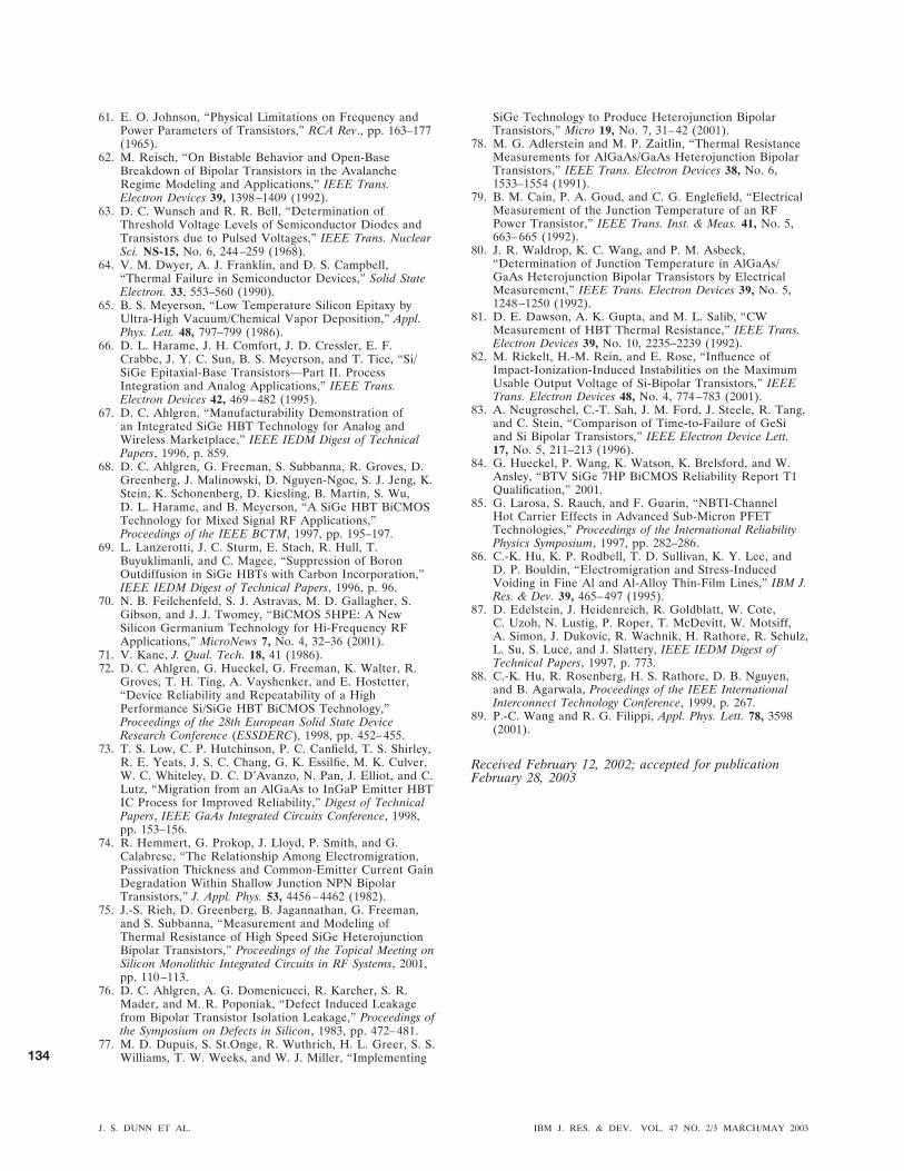
61. E. O. Johnson, “Physical Limitations on Frequency andPower Parameters of Transistors,” RCA Rev., pp. 163–177(1965).
62. M. Reisch, “On Bistable Behavior and Open-BaseBreakdown of Bipolar Transistors in the AvalancheRegime Modeling and Applications,” IEEE Trans.Electron Devices 39, 1398 –1409 (1992).
63. D. C. Wunsch and R. R. Bell, “Determination ofThreshold Voltage Levels of Semiconductor Diodes andTransistors due to Pulsed Voltages,” IEEE Trans. NuclearSci. NS-15, No. 6, 244 –259 (1968).
64. V. M. Dwyer, A. J. Franklin, and D. S. Campbell,“Thermal Failure in Semiconductor Devices,” Solid StateElectron. 33, 553–560 (1990).
65. B. S. Meyerson, “Low Temperature Silicon Epitaxy byUltra-High Vacuum/Chemical Vapor Deposition,” Appl.Phys. Lett. 48, 797–799 (1986).
66. D. L. Harame, J. H. Comfort, J. D. Cressler, E. F.Crabbe, J. Y. C. Sun, B. S. Meyerson, and T. Tice, “Si/SiGe Epitaxial-Base Transistors—Part II. ProcessIntegration and Analog Applications,” IEEE Trans.Electron Devices 42, 469 – 482 (1995).
67. D. C. Ahlgren, “Manufacturability Demonstration ofan Integrated SiGe HBT Technology for Analog andWireless Marketplace,” IEEE IEDM Digest of TechnicalPapers, 1996, p. 859.
68. D. C. Ahlgren, G. Freeman, S. Subbanna, R. Groves, D.Greenberg, J. Malinowski, D. Nguyen-Ngoc, S. J. Jeng, K.Stein, K. Schonenberg, D. Kiesling, B. Martin, S. Wu,D. L. Harame, and B. Meyerson, “A SiGe HBT BiCMOSTechnology for Mixed Signal RF Applications,”Proceedings of the IEEE BCTM, 1997, pp. 195–197.
69. L. Lanzerotti, J. C. Sturm, E. Stach, R. Hull, T.Buyuklimanli, and C. Magee, “Suppression of BoronOutdiffusion in SiGe HBTs with Carbon Incorporation,”IEEE IEDM Digest of Technical Papers, 1996, p. 96.
70. N. B. Feilchenfeld, S. J. Astravas, M. D. Gallagher, S.Gibson, and J. J. Twomey, “BiCMOS 5HPE: A NewSilicon Germanium Technology for Hi-Frequency RFApplications,” MicroNews 7, No. 4, 32–36 (2001).
71. V. Kane, J. Qual. Tech. 18, 41 (1986).72. D. C. Ahlgren, G. Hueckel, G. Freeman, K. Walter, R.
Groves, T. H. Ting, A. Vayshenker, and E. Hostetter,“Device Reliability and Repeatability of a HighPerformance Si/SiGe HBT BiCMOS Technology,”Proceedings of the 28th European Solid State DeviceResearch Conference (ESSDERC), 1998, pp. 452– 455.
73. T. S. Low, C. P. Hutchinson, P. C. Canfield, T. S. Shirley,R. E. Yeats, J. S. C. Chang, G. K. Essilfie, M. K. Culver,W. C. Whiteley, D. C. D’Avanzo, N. Pan, J. Elliot, and C.Lutz, “Migration from an AlGaAs to InGaP Emitter HBTIC Process for Improved Reliability,” Digest of TechnicalPapers, IEEE GaAs Integrated Circuits Conference, 1998,pp. 153–156.
74. R. Hemmert, G. Prokop, J. Lloyd, P. Smith, and G.Calabrese, “The Relationship Among Electromigration,Passivation Thickness and Common-Emitter Current GainDegradation Within Shallow Junction NPN BipolarTransistors,” J. Appl. Phys. 53, 4456 – 4462 (1982).
75. J.-S. Rieh, D. Greenberg, B. Jagannathan, G. Freeman,and S. Subbanna, “Measurement and Modeling ofThermal Resistance of High Speed SiGe HeterojunctionBipolar Transistors,” Proceedings of the Topical Meeting onSilicon Monolithic Integrated Circuits in RF Systems, 2001,pp. 110 –113.
76. D. C. Ahlgren, A. G. Domenicucci, R. Karcher, S. R.Mader, and M. R. Poponiak, “Defect Induced Leakagefrom Bipolar Transistor Isolation Leakage,” Proceedings ofthe Symposium on Defects in Silicon, 1983, pp. 472– 481.
77. M. D. Dupuis, S. St.Onge, R. Wuthrich, H. L. Greer, S. S.Williams, T. W. Weeks, and W. J. Miller, “Implementing
SiGe Technology to Produce Heterojunction BipolarTransistors,” Micro 19, No. 7, 31– 42 (2001).
78. M. G. Adlerstein and M. P. Zaitlin, “Thermal ResistanceMeasurements for AlGaAs/GaAs Heterojunction BipolarTransistors,” IEEE Trans. Electron Devices 38, No. 6,1533–1554 (1991).
79. B. M. Cain, P. A. Goud, and C. G. Englefield, “ElectricalMeasurement of the Junction Temperature of an RFPower Transistor,” IEEE Trans. Inst. & Meas. 41, No. 5,663– 665 (1992).
80. J. R. Waldrop, K. C. Wang, and P. M. Asbeck,“Determination of Junction Temperature in AlGaAs/GaAs Heterojunction Bipolar Transistors by ElectricalMeasurement,” IEEE Trans. Electron Devices 39, No. 5,1248 –1250 (1992).
81. D. E. Dawson, A. K. Gupta, and M. L. Salib, “CWMeasurement of HBT Thermal Resistance,” IEEE Trans.Electron Devices 39, No. 10, 2235–2239 (1992).
82. M. Rickelt, H.-M. Rein, and E. Rose, “Influence ofImpact-Ionization-Induced Instabilities on the MaximumUsable Output Voltage of Si-Bipolar Transistors,” IEEETrans. Electron Devices 48, No. 4, 774 –783 (2001).
83. A. Neugroschel, C.-T. Sah, J. M. Ford, J. Steele, R. Tang,and C. Stein, “Comparison of Time-to-Failure of GeSiand Si Bipolar Transistors,” IEEE Electron Device Lett.17, No. 5, 211–213 (1996).
84. G. Hueckel, P. Wang, K. Watson, K. Brelsford, and W.Ansley, “BTV SiGe 7HP BiCMOS Reliability Report T1Qualification,” 2001.
85. G. Larosa, S. Rauch, and F. Guarin, “NBTI-ChannelHot Carrier Effects in Advanced Sub-Micron PFETTechnologies,” Proceedings of the International ReliabilityPhysics Symposium, 1997, pp. 282–286.
86. C.-K. Hu, K. P. Rodbell, T. D. Sullivan, K. Y. Lee, andD. P. Bouldin, “Electromigration and Stress-InducedVoiding in Fine Al and Al-Alloy Thin-Film Lines,” IBM J.Res. & Dev. 39, 465– 497 (1995).
87. D. Edelstein, J. Heidenreich, R. Goldblatt, W. Cote,C. Uzoh, N. Lustig, P. Roper, T. McDevitt, W. Motsiff,A. Simon, J. Dukovic, R. Wachnik, H. Rathore, R. Schulz,L. Su, S. Luce, and J. Slattery, IEEE IEDM Digest ofTechnical Papers, 1997, p. 773.
88. C.-K. Hu, R. Rosenberg, H. S. Rathore, D. B. Nguyen,and B. Agarwala, Proceedings of the IEEE InternationalInterconnect Technology Conference, 1999, p. 267.
89. P.-C. Wang and R. G. Filippi, Appl. Phys. Lett. 78, 3598(2001).
Received February 12, 2002; accepted for publicationFebruary 28, 2003
J. S. DUNN ET AL. IBM J. RES. & DEV. VOL. 47 NO. 2/3 MARCH/MAY 2003
134

James S. Dunn IBM Microelectronics Division, Burlingtonfacility, 1000 River Road, Essex Junction, Vermont 05452([email protected]). Dr. Dunn is a Senior TechnologyStaff Member in the IBM Microelectronics Division, EssexJunction, Vermont. He received the B.S., M.E. and Ph.D.degrees in materials science and engineering from theUniversity of Utah in 1983, 1989, and 1989, respectively. In1989 he joined IBM in Essex Junction, where he worked onBiCMOS technology development. Since 1992 Dr. Dunn hasmanaged groups developing conventional silicon- and SiGe-based BiCMOS technologies. He holds 16 patents and hascoauthored 13 papers.
David C. Ahlgren IBM Microelectronics Division, EastFishkill facility, Route 52, Hopewell Junction, New York 12533([email protected]). Dr. Ahlgren received his B.A. degreefrom DePauw University in 1973 and his Ph.D. degree inchemical physics from the University of Michigan in 1979.He joined IBM in Hopewell Junction, New York, in 1979conducting semiconductor process development. His earlywork was in the area of silicon defects resulting from ionimplantation and isolation stress, as well as processintegration issues which led to the development andsubsequent production of the first IBM double polysiliconbipolar technology in 1983. In 1989 his attention turned toSi/SiGe HBTs as the next step in the advancement of IBMbipolar mainframe semiconductor technology. His earlydevice studies, process technology work, and semiconductorproduction experience led him into his role in the AdvancedSemiconductor Technology Center as a Senior Engineer indevice and process development of high-performance Si/SiGeBiCMOS technology and its introduction into manufacturing.Dr. Ahlgren is currently Senior Engineering Manager ofSiGe Advanced BiCMOS Technology Development. He haspublished more than 30 technical papers and holds eightpatents in semiconductor device and process technology.
Douglas D. Coolbaugh IBM Microelectronics Division,Burlington facility, 1000 River Road, Essex Junction, Vermont05452 ([email protected]). Dr. Coolbaugh works at the IBMBurlington, Vermont, facility in SiGe BiCMOS technologydevelopment. He is currently the technical team leader forpassives development.
Natalie B. Feilchenfeld IBM Microelectronics Division,Burlington facility, 1000 River Road, Essex Junction, Vermont05452 ([email protected]). Dr. Feilchenfeld is a SeniorScientist in the BiCMOS Technology Development Departmentat the IBM Essex Junction, Vermont, facility. She receivedan A.B. degree in chemistry from Bryn Mawr Collegein 1979, and M.S. and Ph.D. degrees in chemistry fromCarnegie Mellon University in 1982 and 1983, respectively.After a postdoctoral appointment at the University ofChicago, she joined IBM at the Endicott PackagingDevelopment Laboratory. She worked on photolithographyand on developing new electronic plastic packages. In 1996,Dr. Feilchenfeld joined the Silicon Germanium TechnologyDevelopment Group in Essex Junction, Vermont, where sheand her team have been responsible for the development andqualification of low-complexity SiGe technologies (SiGe5MR,5HPE, and 7WL). She is an author or coauthor of 12 patentsand 22 technical papers. Dr. Feilchenfeld is a member of theAmerican Chemical Society.
Greg Freeman IBM Microelectronics Division, East Fishkillfacility, Route 52, Hopewell Junction, New York 12533([email protected]). Dr. Freeman received his Ph.D.degree in electrical engineering from Stanford University in1991, and has since worked in the IBM MicroelectronicsDivision. He is currently a Senior Engineering Manager,managing a department with responsibility for high-performance SiGe and rf CMOS device design, rfcharacterization, and compact modeling. His research interestsare in the field of rf device optimization and applications. Dr.Freeman is an author or coauthor of four patents and morethan 50 technical papers. He is a Senior Member of theInstitute of Electrical and Electronics Engineers.
David R. Greenberg IBM Research Division, East Fishkillfacility, Route 52, Hopewell Junction, New York 12533([email protected]). Dr. Greenberg is a semiconductordevice researcher working in advanced rf technologydevelopment and assessment. He received a B.S. degree inelectrical engineering at Columbia University under a Pulitzerscholarship in 1988 and completed both his M.S. and Ph.D.degrees at M.I.T under Hertz and Intel Foundationfellowships in 1990 and 1994, respectively. In 1995 Dr.Greenberg joined IBM, where he has played key roles in thedevelopment of five generations of SiGe rf technology,including device design and evaluation, power transistordevelopment, and interfacing with customer technology andcircuit design groups. Most recently, he has become involvedin rf CMOS technology definition. Dr. Greenberg is an authoror coauthor of three patents and more than 30 technicalpapers. He is a member of Tau Beta Pi and the Institute ofElectrical and Electronics Engineers.
Robert A. Groves IBM Microelectronics Division, EastFishkill facility, Route 52, Hopewell Junction, New York 12533([email protected]). Mr. Groves received a B.S.E.E. degreefrom the State University of New York in 1996. He joined theIBM Corporation at the East Fishkill facility in 1989 as aDevelopment Laboratory Technician. Since 1994, he hasworked on SiGe technology development, with an emphasison high-frequency modeling and characterization. His currentfocus is on interconnections, capacitors, and inductors(particularly integrated spiral inductor optimization andmodeling) for microwave integrated circuits.
Fernando J. Guarın IBM Microelectronics Division, EastFishkill facility, Route 52, Hopewell Junction, New York12533 ([email protected]). Dr. Guarın is a SeniorEngineer/Scientist at the IBM Microelectronics SemiconductorResearch Development Center in East Fishkill, New York. Hereceived a B.S.E.E. degree from the Pontificia UniversidadJaveriana, Bogota, Colombia, an M.S.E.E. degree from theUniversity of Arizona, and a Ph.D. in electrical engineeringfrom Columbia University. From 1980 to 1988 he was amember of the Military and Aerospace Operations Division ofNational Semiconductor Corporation, where he held positionsin both engineering and management. In 1988 he joined theIBM Microelectronics Division, where he has worked in thereliability physics of advanced bipolar, CMOS, and SiGetechnologies. Dr. Guarın holds five patents and has publishedmore than 30 papers. He is a Senior Member of the Instituteof Electrical and Electronics Engineers.
IBM J. RES. & DEV. VOL. 47 NO. 2/3 MARCH/MAY 2003 J. S. DUNN ET AL.
135

Youssef Hammad (no biography available)
Alvin J. Joseph IBM Microelectronics Division, Burlingtonfacility, 1000 River Road, Essex Junction, Vermont 05452([email protected]). Dr. Joseph received the B.E. degreein electrical engineering from Bangalore University, India,in 1989 and the M.S. and Ph.D. degrees, both in electricalengineering, from Auburn University in 1992 and 1997,respectively. His doctoral research involved the study ofphysics, optimization, and modeling of cryogenically operatedSiGe HBTs. In 1997, he joined the IBM MicroelectronicsDivision in Essex Junction, Vermont. He has been involved inintegration and device design aspects of several generationsof SiGe BiCMOS technologies. Dr. Joseph was the leadtechnologist/process integrator for the IBM 0.18-�m 120-GHzSiGe BiCMOS technology for production. He is a SeniorEngineer and manages the SiGe technology developmentgroup responsible for installing high-speed SiGe BiCMOStechnologies for production. Dr. Joseph has authored andco-authored several technical journal papers and conferencepublications related to SiGe devices and technologies. He hasbeen a member of the device physics subcommittee for theIEEE Bipolar/BiCMOS Circuits and Technology Meeting andis currently serving the process technology subcommittee inthe IEEE Bipolar/BiCMOS Circuits and Technology Meeting.Dr. Joseph is a Senior Member of the IEEE.
Louis D. Lanzerotti IBM Microelectronics Division,Burlington facility, 1000 River Road, Essex Junction, Vermont05452 ([email protected]). Dr. Lanzerotti is a Process andDevice Engineer with the SiGe Technology DevelopmentTeam in Essex Junction, Vermont. He received his B.S.degree in applied and engineering physics from CornellUniversity and his Ph.D. degree in electrical engineering fromPrinceton University.
Stephen A. St.Onge IBM Microelectronics Division,Burlington facility, 1000 River Street, Essex Junction, Vermont05452 ([email protected]). Mr. St.Onge is currentlyManager of the Mixed Signal Technology DevelopmentDepartment at the IBM Microelectronics manufacturingfacility in Essex Junction, Vermont. He has worked at thatlocation since 1982, focusing on bipolar, BiCMOS, and SiGeBiCMOS technology development. He received a B.S. degreein electrical engineering from the University of Vermont in1992. Mr. St.Onge is an author or coauthor of 13 patents andseveral technical papers. He is a member of the IEEE.
Bradley A. Orner IBM Microelectronics Division, Burlingtonfacility, 1000 River Road, Essex Junction, Vermont 05452([email protected]). Dr. Orner is an Advisory Engineer inthe SiGe BiCMOS Technology Development Department.He received a B.S. degree in electrical engineering fromJohns Hopkins University in 1989, an M.S. degree in electricalengineering in 1995, and a Ph.D. in electrical engineering in1997, both from the University of Delaware. Dr. Ornersubsequently joined IBM at the Semiconductor Researchand Development Center in Essex Junction, Vermont.
Jae-Sung Rieh IBM Microelectronics Division, EastFishkill facility, Route 52, Hopewell Junction, New York 12533
([email protected]). Dr. Rieh is an Advisory Engineer in theEarly Technology Definition and Evaluation Department atthe IBM Microelectronics Division facility in HopewellJunction, New York. He received B.S. and M.S. degreesin electronics engineering from Seoul National University,Korea, in 1991 and 1995, respectively, and a Ph.D. degree inelectrical engineering from the University of Michigan in1999. His doctoral research involved the development ofSiGe-based electrical and optical devices and their applicationto microwave and optoelectronic integrated circuits. In 1999,Dr. Rieh joined the IBM Microelectronics Division in EssexJunction, Vermont, as a characterization engineer. Since2000, he has been with IBM Semiconductor Research andDevelopment Center, Hopewell Junction, New York, wherehe is involved in the design and characterization of high-speedSiGe HBTs for analog and mixed-signal applications and theanalysis and modeling of the thermal and avalanche behaviorof SiGe HBTs.
Kenneth J. Stein IBM Microelectronics Division, EastFishkill facility, Route 52, Hopewell Junction, New York 12533([email protected]). Mr. Stein is an Advisory Engineer inthe Silicon Germanium BiCMOS Department in East Fishkill.He received B.S. degrees in paper science engineering fromSUNY ESF and chemical engineering from Syracuse Universityin 1982 and 1983, respectively. After two years at FairchildSemiconductor, he joined IBM at the Thomas J. WatsonResearch Center, Yorktown Heights, New York, wherehe worked in the Advanced Silicon Technology facility,holding both process development and management positions.Since 1993, Mr. Stein has worked in the SemiconductorResearch Development Center, first in MUV lithography and,for the past eight years, on the Silicon Germanium BiCMOSDevelopment team, with responsibilities in the areas ofFEOL, BEOL, and passives process integration. Mr. Steinholds a number of patents in the areas of capacitor andinductor fabrication.
Steven H. Voldman IBM Microelectronics Division,Burlington facility, 1000 River Road, Essex Junction, Vermont05452 ([email protected]). Dr. Voldman is a memberof the Silicon Germanium Development team at the IBMmanufacturing facility in Essex Junction, Vermont. Hereceived a B.S. degree in engineering science from theUniversity of Buffalo in 1979; an M.S. degree in electricalengineering and an E.E. degree from the MassachusettsInstitute of Technology in 1981 and 1982; and an M.S.degree in engineering physics and a Ph.D. degree in electricalengineering from the University of Vermont in 1986 and 1991,respectively. In 1982, he joined IBM, working on alpha-particle effects on bipolar SRAMs; he was a member of theIBM 4-Mb DRAM, 16-Mb DRAM, CMOS logic, SOI, andSiGe technology teams. He is an author of more than 100U.S. issued patents and 100 technical papers. Dr. Voldman isan Institute of Electrical and Electronics Engineers (IEEE)Fellow for his contributions to electrostatic discharge (ESD)in CMOS, SOI, and silicon germanium technologies.
Ping-Chuan Wang IBM Microelectronics Division, EastFishkill facility, Route 52, Hopewell Junction, New York12533 ([email protected]). Dr. Wang is an AdvisoryScientist/Engineer in the Technology Reliability EngineeringDepartment, where his work involves the fundamental studyand modeling of reliability in electronic thin-film materialsand devices. He received his doctoral degree in materials
J. S. DUNN ET AL. IBM J. RES. & DEV. VOL. 47 NO. 2/3 MARCH/MAY 2003
136

science from Columbia University in 1997 under an IBMCooperative Fellowship. After an appointment as a VisitingScientist at Lehigh University, Dr. Wang joined the IBMMicroelectronics Division in 1997. His current researchinterests include the development and application of asynchrotron-based X-ray microbeam system to study materialproperties in micron scale. Dr. Wang is an author or co-author of more than 30 technical papers and one U.S. patent.
Michael J. Zierak IBM Microelectronics Division,Burlington facility, 1000 River Road, Essex Junction, Vermont05452 ([email protected]). Dr. Zierak received B.S., M.S.,and Ph.D. degrees in electrical engineering from RensselaerPolytechnic Institute in 1991, 1992, and 1997, respectively.His doctoral studies involved InGaAs and InGaAsSb materialengineering and device design for thermophotovoltaic powergeneration. Since joining IBM in 1997, he has worked onprocess integration and device design in SiGe BiCMOStechnologies. Dr. Zierak is currently an Advisory Engineerin the SiGe Technology Development Department.
Seshadri Subbanna IBM Systems Group, 2455 SouthRoad, Poughkeepsie, New York 12601 ([email protected]).Dr. Subbanna received his B. Tech. degree in electricalengineering from the Indian Institute of Technology, Bombay,and his M.S.E.E. degree and Ph.D. degree in electricalengineering and materials science from the University ofCalifornia at Santa Barbara. His doctoral work was on opticaland electronic properties of antimonide superlattices andheterostructures, including the first observation of quadraticpiezo-electro-optic effect in strained superlattices. From 1989to 2002, Dr. Subbanna was with the IBM MicroelectronicsDivision in East Fishkill, New York. Since joining IBM, hehas worked on advanced bipolar and CMOS processes, high-density SRAM development, and BiCMOS technology. From1996 to 2002, he was manager of advanced silicon– germanium(SiGe) heterojunction bipolar transistor (HBT) BiCMOSdevelopment at the IBM Microelectronics SemiconductorResearch and Development Center in East Fishkill. Thisgroup was the first to achieve over 200 GHz high-frequencyperformance in a silicon-based technology, and it isrecognized worldwide as a leader in the development of high-speed networking technology. He was also a senior businesscounsel charged with intellectual property development andpatent generation. Currently Dr. Subbanna is on assignmentwith the IBM Systems Group (previously the IBM ServerGroup). He has given many invited talks, and has over 50publications and 20 patents to his credit.
David L. Harame IBM Microelectronics Division, Burlingtonfacility, 1000 River Road, Essex Junction, Vermont 05452([email protected]). Dr. Harame received a B.A. degreein zoology from the University of California at Berkeley in1971 and an M.S. degree in zoology from Duke Universityin 1973. He also received an M.S. degree in electricalengineering from San Jose State University in 1976 and anM.S. degree in materials science and a Ph.D. in electricalengineering, both from Stanford University in 1984. Hethen joined the IBM bipolar technology group at the IBMThomas J. Watson Research Center, where he worked on thefabrication and modeling of Si-based integrated circuits. Hisresearch interests at Yorktown Heights included Si transistors,SiGe-channel FET transistors, npn and pnp SiGe-base bipolartransistors, complementary bipolar technology, and BiCMOStechnology for digital and analog and mixed-signal
applications. In 1993 he joined the IBM SemiconductorResearch and Development Center in the AdvancedSemiconductor Technology Center (ASTC) in HopewellJunction, New York, where he was responsible for thedevelopment of SiGe technology for mixed-signal applications.He managed SiGe BiCMOS technology development at theASTC through 1997. In 1998 Dr. Harame joined the IBMmanufacturing organization in Essex Junction, Vermont,where he managed a SiGe technology group and theinstallation of the 0.5-mm SiGe BiCMOS process intomanufacturing. In 1999 he co-managed the qualification of a0.25-�m SiGe BiCMOS as well as 0.18-�m SiGe BiCMOSand two derivative SiGe BiCMOS technologies. In 2000, hebecame the Senior Manager of the RF Analog Modelingand Design Kit Department. Dr. Harame is a DistinguishedEngineer of the IBM Corporation, a Senior Member ofthe IEEE, an Executive Committee member of theBipolar/BiCMOS Circuits and Technology Meeting (BCTM),and a member of the Compact Model Council.
Dean A. Herman, Jr. IBM Thomas J. Watson ResearchCenter, P.O. Box 218, Yorktown Heights, New York 10598([email protected]). Dr. Herman is Manager of Analog andMixed Signal Operations, Office of the Chief Technologist,IBM Technology Group. Until recently he managed thegroups doing research and development on the IBM SiGetechnologies and on the design kits for all IBM analog andmixed-signal technologies; this effort included the IBM high-frequency measurement and modeling efforts. Dr. Hermanreceived a B.S. degree in engineering from the U.S. MilitaryAcademy at West Point, New York, in 1960, and M.S. andPh.D. degrees in electrical engineering from StanfordUniversity in 1967 and 1975, respectively. He taught in theDepartment of Electrical Engineering at West Point for 15years and was Professor and Deputy Head of the Departmentprior to joining IBM in 1986. He is a Senior Member of theInstitute of Electrical and Electronics Engineers.
Bernard S. Meyerson IBM Thomas J. Watson ResearchCenter, P.O. Box 218, Yorktown Heights, New York 10598([email protected]). Dr. Meyerson is Chief Technologist,IBM Technology Group, also serving as Vice President, IBMCommunication Research and Development Center. Hereceived a Ph.D. degree in solid-state physics from the CityCollege of the City University of New York in 1980 andsubsequently joined IBM at the Thomas J. Watson ResearchCenter to work on the chemical fundamentals of electronicmaterials thin-film deposition. His work led to thedevelopment of ultrahigh-vacuum/chemical vapor deposition(UHV/CVD), a technique which proved successful for theepitaxial deposition of a wide variety of Si-based alloys underconditions, and having chemical compositions which lay welloutside accepted bounds on such processes and materials.Most significant was the deposition of production quantitiesof SiGe epitaxial layers at temperatures of 500 C and below,resulting in the development of extremely high-performanceSiGe heterjunction bipolar transistors (HBTs). Under hisleadership, a complete SiGe HBT technology was developed,demonstrating high levels of integration at performancecharacteristics representing a discontinuity in historical trendsfor bipolar technology. Although the technology was initiallyintended for computing applications, Dr. Meyerson refocusedit into a communication-centric technology. By 1992, he hadlaunched a series of now well-publicized IBM alliances toleverage this technology trend, over the years incorporatingorganizations as diverse as Alcatel, Analog Devices, Hughes,Harris Semiconductor (now Intersil), Leica, National
IBM J. RES. & DEV. VOL. 47 NO. 2/3 MARCH/MAY 2003 J. S. DUNN ET AL.
137

Semiconductor, Nortel, Tektronix, and many others. Earlyadoption of the technology has led to numerous commercialand consumer products, 40-Gb/s SONET standard datasystems and 802.11b 11-Mb/s wireless LAN cards beinglimited examples. IBM’s lead into this marketplace hasresulted in general technology acceptance after ten yearsof controversy, with all major communications technologyproviders announcing upcoming, competing market entries.In 1998, the IBM analog and mixed-signal technologydevelopment was consolidated under Dr. Meyerson. In 2002,he became Vice President of the Communications Researchand Development Center, a multinational organizationencompassing IBM’s worldwide communications technologyand circuit design efforts and supporting a rapidly growingworldwide customer base. In 1992, Dr. Meyerson wasdesignated as an IBM Fellow. He is also a Fellow of theAmerican Physical Society and the IEEE. He holds morethan 40 patents and has published several hundred technicalpapers. He has received numerous awards for his work,including the Materials Research Society Medal (1991) andthe Electrochemical Society Electronics Division Award(1993); he was cited as “Inventor of the Year 1997” by theNew York State Legislature and was honored as the 1999“United States Distinguished Inventor of the Year” by theU.S. Patent and Trademark Office. He recently receivedthe 1999 IEEE Ernst Weber Award for the body of workculminating in the commercialization of SiGe-basedcommunications technology. In December 1999, he receivedthe IEEE Electron Devices Society J. J. Ebers Award, andin 2002 he was inducted into the National Academy ofEngineering. His team’s work has been featured in along-term ongoing study by the Lally School of BusinessManagement, exploring the management of discontinuousinnovation within large organizations.
J. S. DUNN ET AL. IBM J. RES. & DEV. VOL. 47 NO. 2/3 MARCH/MAY 2003
138