Embed Size (px)
Citation preview
1Sorin Voinigescu et al. CSICS-2005, Nov. 2nd, 2005
Design Methodology and Applications of SiGe BiCMOS Design Methodology and Applications of SiGe BiCMOS Cascode Opamps with up to 37-GHz Unity Gain Cascode Opamps with up to 37-GHz Unity Gain
BandwidthBandwidth
S.P. Voinigescu, R. Beerkens*, T.O. Dickson, and T. Chalvatzis
University of Toronto*STMicroelectronics, Ottawa

2Sorin Voinigescu et al. CSICS-2005, Nov. 2nd, 2005
OutlineOutline
IntroductionOpamp designApplication to 1.2-GHz bandpass filterConclusions
3Sorin Voinigescu et al. CSICS-2005, Nov. 2nd, 2005
MotivationMotivation
Opamps are useful in a variety of low-cost RF applications
Opamp UGB has not kept pace with MOS/HBT fT/fMAX
GoalGoalDesign methodology for large UGB opamps with good phase margin
4Sorin Voinigescu et al. CSICS-2005, Nov. 2nd, 2005
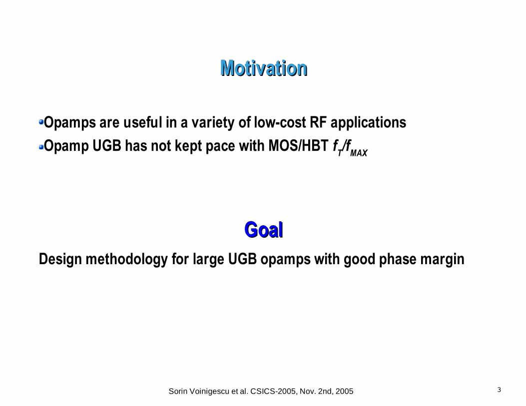
Challenges for opamp design in nanoscale (Bi)CMOSChallenges for opamp design in nanoscale (Bi)CMOS
Square-law in sub 130-nm MOSFETs invalid for most bias range
Traditional biasing at low Veff makes nanoscale CMOS opamps suffer
from
sensitive to PVT variation
modest bandwidth
poor linearity
model inaccuracy

5Sorin Voinigescu et al. CSICS-2005, Nov. 2nd, 2005
How do we maximize opamp bandwidth?How do we maximize opamp bandwidth?
By selecting a high-bandwidth topology with good stability
By (unconventionally) biasing and sizing transistors for high UGB

6Sorin Voinigescu et al. CSICS-2005, Nov. 2nd, 2005
Topology: MOS-HBT cascode with p-MOS cascode loadTopology: MOS-HBT cascode with p-MOS cascode load
Miller effect completely eliminatedGood gain: A
V = g
mn*g
mpr2
op
Unlike HBT-HBT cascode, input time constant R
G(C
gs + C
gd + C
pad) is
minimized through layout (RG)
Dominant pole at output
UGB=g
m ,nMOS
2Cout
Cout=CbcCcsCdb,pMOSCgd,pMOSCL
VDD
= 3.3 V
VOUT
VIN
20*0.130um*2um
28*0.150um *4um
0.180um*10um
8..10 mA
VBIAS
= 1.8 V
CPAD
= 40 fF
CPAD
= 40 fF
Single-pole frequency response beyond

7Sorin Voinigescu et al. CSICS-2005, Nov. 2nd, 2005
Opamp biasing Opamp biasing HBT biased at peak f
MAX current density (1.2 mA/µm)
MOSFETs biased at peak fMAX
current density (0.2 mA/µm)
fMAX
and gain remain flat for IDS
= 0.15 to 0.4 mA/µm
170 GHz @ 0.14 mW/µm of gate finger width
8Sorin Voinigescu et al. CSICS-2005, Nov. 2nd, 2005
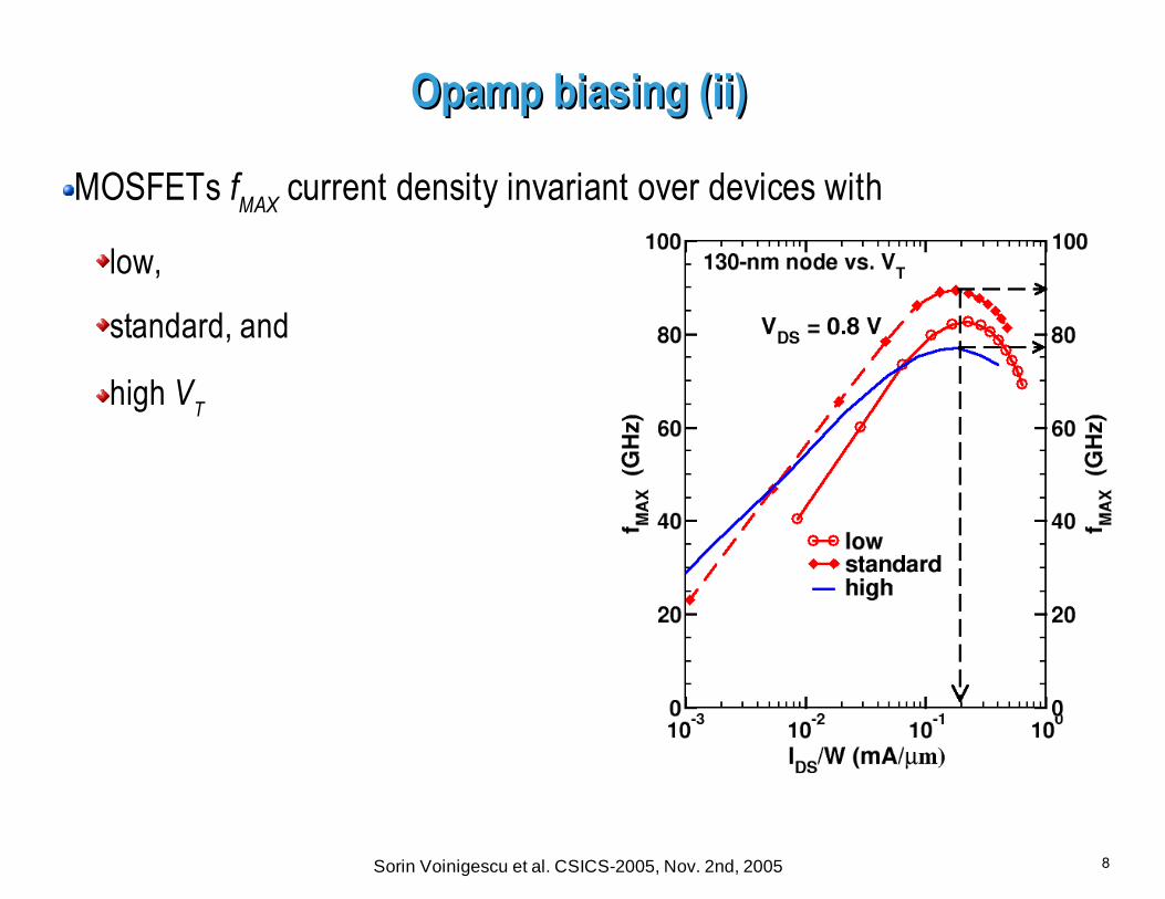
Opamp biasing (ii) Opamp biasing (ii)
MOSFETs fMAX
current density invariant over devices with
low,
standard, and
high VT
9Sorin Voinigescu et al. CSICS-2005, Nov. 2nd, 2005
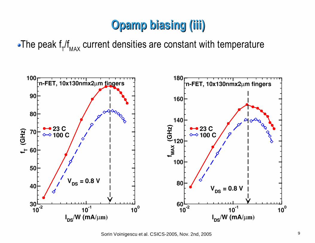
Opamp biasing (iii)Opamp biasing (iii)
The peak fT/f
MAX current densities are constant with temperature
10Sorin Voinigescu et al. CSICS-2005, Nov. 2nd, 2005
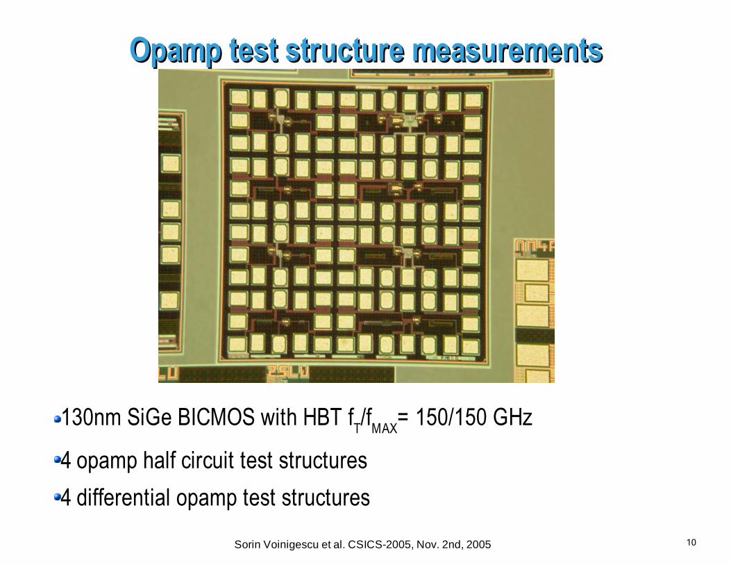
Opamp test structure measurementsOpamp test structure measurements
130nm SiGe BICMOS with HBT fT/f
MAX= 150/150 GHz
4 opamp half circuit test structures
4 differential opamp test structures

11Sorin Voinigescu et al. CSICS-2005, Nov. 2nd, 2005
Opamp half ckt. DC transfer characteristicsOpamp half ckt. DC transfer characteristics
5 mA and 10 mA versions
36 dB gain at 0.25 mA/µm in both
VOMAX
= 2.8 V
VOMIN
= 1 V
12Sorin Voinigescu et al. CSICS-2005, Nov. 2nd, 2005
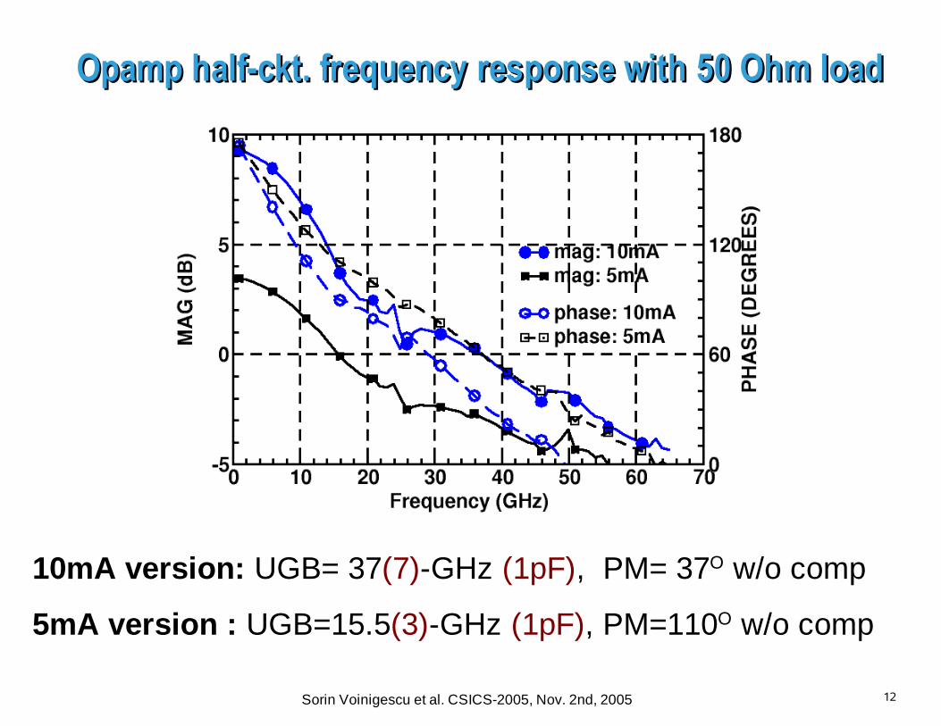
Opamp half-ckt. frequency response with 50 Ohm loadOpamp half-ckt. frequency response with 50 Ohm load
10mA version: UGB= 37(7)-GHz (1pF), PM= 37O w/o comp
5mA version : UGB=15.5(3)-GHz (1pF), PM=110O w/o comp
13Sorin Voinigescu et al. CSICS-2005, Nov. 2nd, 2005
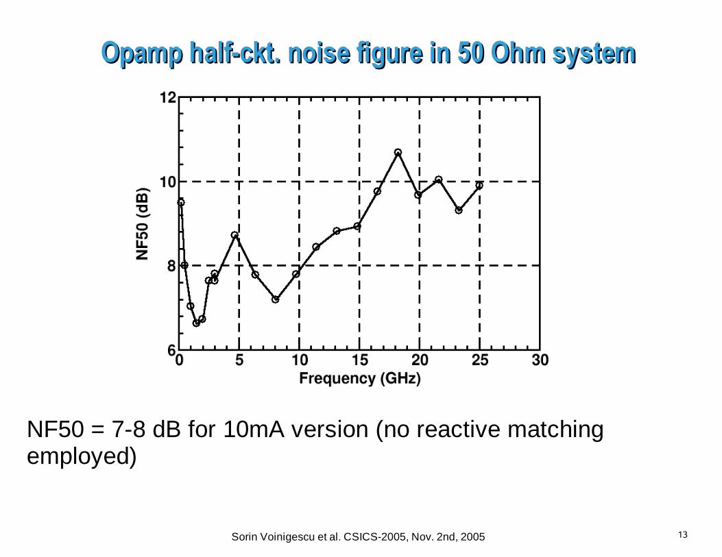
Opamp half-ckt. noise figure in 50 Ohm systemOpamp half-ckt. noise figure in 50 Ohm system
NF50 = 7-8 dB for 10mA version (no reactive matching employed)

14Sorin Voinigescu et al. CSICS-2005, Nov. 2nd, 2005
Half ckt. UGB vs. MOSFET current densityHalf ckt. UGB vs. MOSFET current density
Opamp reaches maximum UGB beyond the peak fMAX
current density
UGB varies by less than 10% for IDS
= 0.2 to 0.4 mA/µm
15Sorin Voinigescu et al. CSICS-2005, Nov. 2nd, 2005
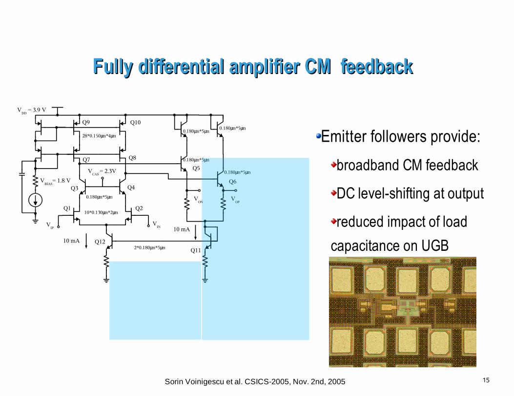
Fully differential amplifier CM feedback Fully differential amplifier CM feedback
VDD
= 3.9 V
VCAS
= 2.3V
VIP
10*0.130µm*2µm
28*0.150µm*4µm
0.180µm*5µm
10 mA
VBIAS
= 1.8 V
10 mAV
IN
VON
VOP
Q1 Q2
Q3 Q4
Q5
Q6
Q7 Q8
Q9 Q10
Q11
Q122*0.180µm*5µm
0.180µm*5µm
0.180µm*5µm
0.180µm*5µm0.180µm*5µm Emitter followers provide:
broadband CM feedback
DC level-shifting at output
reduced impact of load
capacitance on UGB
16Sorin Voinigescu et al. CSICS-2005, Nov. 2nd, 2005
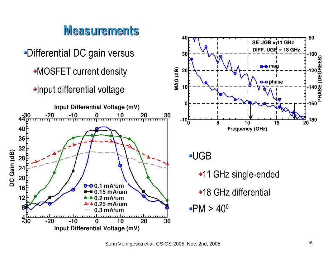
Measurements Measurements
Differential DC gain versus
MOSFET current density
Input differential voltage
UGB
11 GHz single-ended
18 GHz differential
PM > 400

17Sorin Voinigescu et al. CSICS-2005, Nov. 2nd, 2005
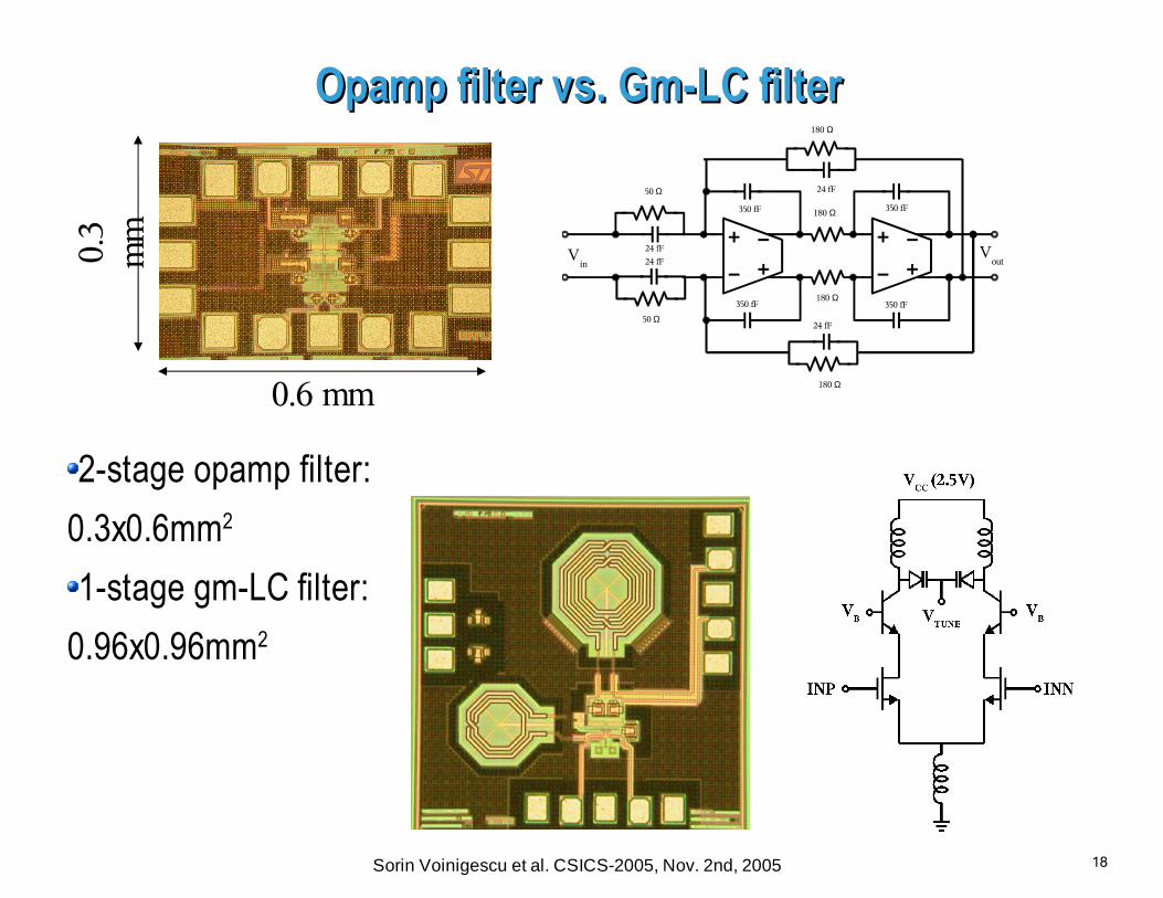
1.2-GHz biquad bandpass filter1.2-GHz biquad bandpass filter180 Ω
180 Ω
180 Ω
180 Ω
50 Ω
50 Ω
350 fF
350 fF 350 fF
350 fF
24 fF
24 fF
24 fF
24 fFVin
Vout
0.3
mm
0.6 mm
18Sorin Voinigescu et al. CSICS-2005, Nov. 2nd, 2005
Opamp filter vs. Gm-LC filterOpamp filter vs. Gm-LC filter
2-stage opamp filter:
0.3x0.6mm2
1-stage gm-LC filter:
0.96x0.96mm2
180 Ω
180 Ω
180 Ω
180 Ω
50 Ω
50 Ω
350 fF
350 fF 350 fF
350 fF
24 fF
24 fF
24 fF
24 fFVin
Vout0.
3 m
m
0.6 mm
19Sorin Voinigescu et al. CSICS-2005, Nov. 2nd, 2005
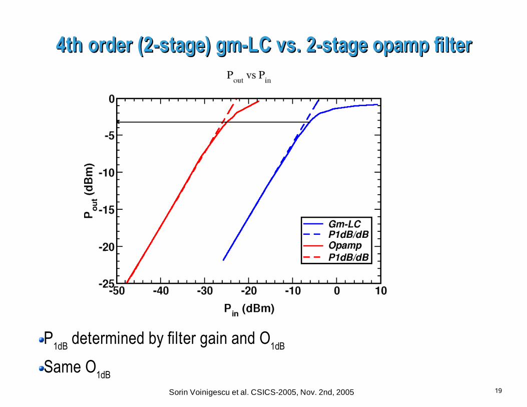
4th order (2-stage) gm-LC vs. 2-stage opamp filter4th order (2-stage) gm-LC vs. 2-stage opamp filter
P1dB determined by filter gain and O1dB
Same O1dB
20Sorin Voinigescu et al. CSICS-2005, Nov. 2nd, 2005
SummarySummary
MOS-HBT cascode topology maximizes UGB with good stability
Radical approach to biasing CMOS-based opamps at peak fMAX
current
density ensures:
maximum UGB
robustness to ID, T, L, VT variation
good linearity
1.2-GHz Biquad filter with 2 opamps and CMF demonstratedLinearity & power comparable to g
m-LC filter but 5x area reduction
Portable between 130-nm and 180-nm nodes (G. Ng et al. SiRF 2006)

21Sorin Voinigescu et al. CSICS-2005, Nov. 2nd, 2005
AcknowledgementsAcknowledgements
Bernard Sautreuil & Steve McDowall of STMicroelectronics
CFI, OIT and NIT for equipment
22Sorin Voinigescu et al. CSICS-2005, Nov. 2nd, 2005
BackupBackup
23Sorin Voinigescu et al. CSICS-2005, Nov. 2nd, 2005
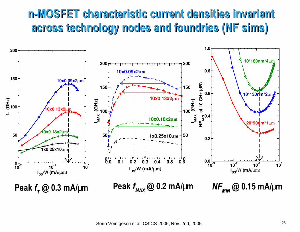
n-MOSFET characteristic current densities invariant n-MOSFET characteristic current densities invariant across technology nodes and foundries (NF sims)across technology nodes and foundries (NF sims)
Peak fT @ 0.3 mA/µm Peak fMAX @ 0.2 mA/µm NFMIN
@ 0.15 mA/µm
24Sorin Voinigescu et al. CSICS-2005, Nov. 2nd, 2005
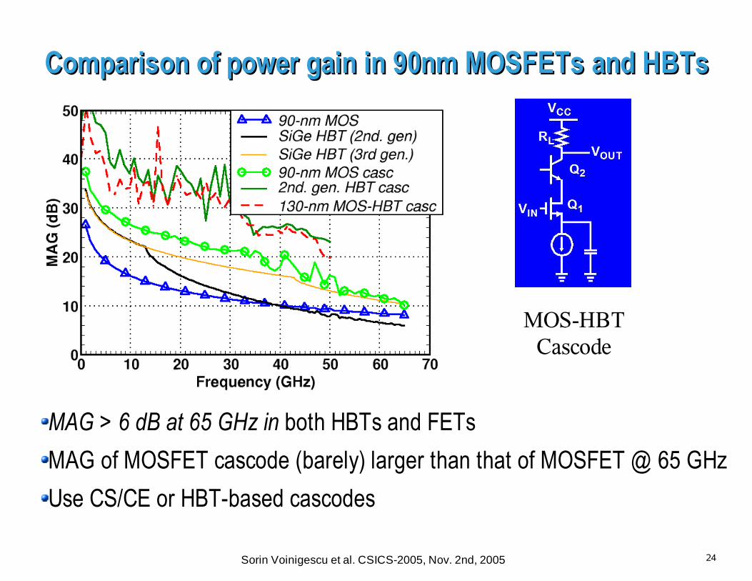
Comparison of power gain in 90nm MOSFETs and HBTsComparison of power gain in 90nm MOSFETs and HBTs
MOS-HBTCascode
MAG > 6 dB at 65 GHz in both HBTs and FETs
MAG of MOSFET cascode (barely) larger than that of MOSFET @ 65 GHz
Use CS/CE or HBT-based cascodes
25Sorin Voinigescu et al. CSICS-2005, Nov. 2nd, 2005
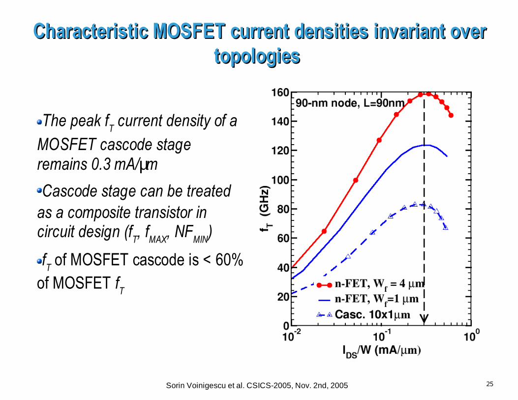
Characteristic MOSFET current densities invariant over Characteristic MOSFET current densities invariant over topologies topologies
The peak fT current density of a
MOSFET cascode stage remains 0.3 mA/µm
Cascode stage can be treated as a composite transistor in circuit design (f
T, f
MAX, NF
MIN)
fT of MOSFET cascode is < 60%
of MOSFET fT
26Sorin Voinigescu et al. CSICS-2005, Nov. 2nd, 2005
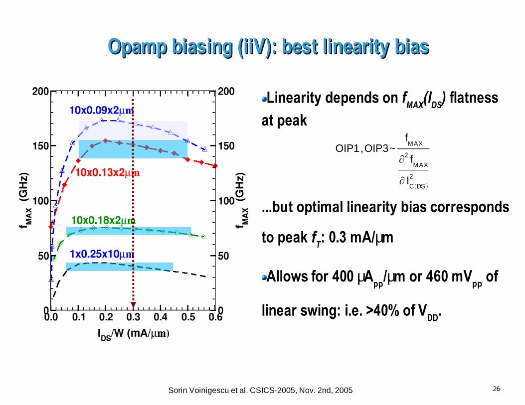
Opamp biasing (iiV): best linearity biasOpamp biasing (iiV): best linearity bias
Linearity depends on fMAX(IDS) flatness at peak
...but optimal linearity bias corresponds
to peak fT: 0.3 mA/µm
Allows for 400 µApp/µm or 460 mVpp of
linear swing: i.e. >40% of VDD.
OIP1,OIP3~fMAX
∂2 fMAX
∂ ICDS 2
27Sorin Voinigescu et al. CSICS-2005, Nov. 2nd, 2005
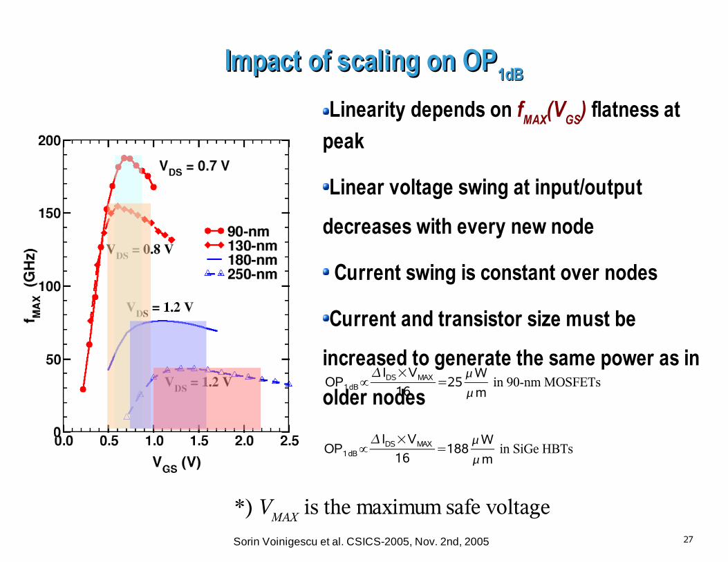
Impact of scaling on OPImpact of scaling on OP1dB1dB
Linearity depends on fMAX
(VGS
) flatness at
peak
Linear voltage swing at input/output
decreases with every new node
Current swing is constant over nodes
Current and transistor size must be
increased to generate the same power as in
older nodesOP1dB∝
IDS×VMAX16
=25Wm
in 90-nm MOSFETs
OP1dB∝ IDS×VMAX
16=188
Wm
in SiGe HBTs
*) VMAX
is the maximum safe voltage
28Sorin Voinigescu et al. CSICS-2005, Nov. 2nd, 2005
ConclusionsConclusions
CMOS characteristic densities largely invariant across nodes and foundries
Constant-current density biasing in analog/RF CMOS minimizes impact of L, I
DS, T, and V
T variation
Characteristic current densities in MOSFETs are invariant over topologies (CS, MOS-MOS and MOS-HBT)
Implications for circuit designImplications for circuit designCMOS CML gates, LNAs, TIAs, Opamps, VCOs, Mixers, PAs can be
designed algorithmically and ported across nodes and technologies