Embed Size (px)
Citation preview

FORMATION OF CuAlO2 THIN FILMS BY
ULTRASONIC SPRAY PYROLYSIS FOR PHOTODIODE
APPLICATIONS
Iping Suhariadi
UNIVERSITI SAINS MALAYSIA
2011
i
FORMATION OF CUAlO2 THIN FILMS BY
ULTRASONIC SPRAY PYROLYSIS FOR
PHOTODIODE APPLICATIONS
by
IPING SUHARIADI
Thesis submitted in fulfillment of the requirements
for the Degree of
Master of Science
August 2011

ii
ACKNOWLEDGEMENTS
Firstly, I would like to thank to Allah SWT for His mercy enabling me to
compose this thesis. May peace be upon our beloved Prophet, Muhammad SAW. I
would like to thank to my main supervisor, Assoc.Prof.Dr. Zainovia Lockman for her
continuous effort in supervision, encouragement and her helps when I was facing any
obstacles during my research. I also like to thank my Co-supervisor, Assoc.Prof.Dr.
Sabar D. Hutagalung for all of his advice and support. I would also like to thank to
Prof. Kamsul Abraha for his assistance and Prof. Matsuda Atsunori for his advice
regarding this research.
I would like to the thank Dean of PPKBSM Prof. Dr. Ahmad Fauzi Mohd
Noor and to all academic, administrative and technical staffs of the PPKBSM for their
kind assistance and supports. Especially Mr. Suhaimi, Mrs. Fong, Mr. Sahrul, Mr.
Zaini, Mr. Azam, and Mr. Rashid. I would also thank to all technical staffs from Nano
Optoelectronic Research (NOR) lab of the School of Physics, USM for their assistance
and technical support during my MSc works.
I would like to show my deepest gratitude to AUN/SEED-Net JICA for the
financial support (2009-2011). My sincere thanks to the AUN/SEED-Net JICA team,
Mr. Takahashi, Ms. Siriporn, Ms. Kanchana, Ms. Karnkitti and USM international
office staffs: Mrs. Irda, Mrs. Norpisah.
Many thanks to all of the Electronic Laboratory Members, P‘Teguh, Kak Sya,
Cheah Li, Mas Cahyo. I wish to thank to all of postgraduate students in PPKBSM
USM and AUN/SEED-Net friends, Mr. Villay, Ms. Bhum, Ann, Mr. Phat, Mr. Toung,
iii
Phanny, Lin. I also want to thanks to my Indonesian friends Bapak and Ibu Syaf, P‘
Shamsuddin and family, P‘ Subhi and Family, P‘ Sudibyo, P‘fathur, Niken, Alm. P‘
Martunus, P‘Syamsiro, P‘Djanter, Imam, P‘Dadan, P‘Tri, P‘Dadan, Sunarso.
Finally, I want to take this opportunity to show my special thanks to my
family, my mom and my dad. Thank you for your endless love and support. I dedicate
this thesis for them.
Thank you all.
Iping Suhariadi

iv
TABLE OF CONTENTS
Page
ACKNOWLEDGMENTS ii
TABLE OF CONTENTS iv
LIST OF TABLES viii
LIST OF FIGURES ix
LIST OF ABBREVIATION xiii
LIST OF SYMBOLS xiv
LIST OF PUBLICATIONS xv
ABSTRAK xvi
ABSTRACT xvii
CHAPTER 1: INTRODUCTION
1.1 Introduction 1
1.2 Problem statement 2
1.3 Objectives of the research 5
1.4 Scope of study 5
1.5 Thesis structure 6
CHAPTER 2: LITERATURE REVIEW
2.1 Introduction 7
2.2 Transparent Conducting Oxides (TCOs) 9
2.2.1 N-type semiconductor 9
v
2.2.2 P-type semiconductor 11
2.2.2.1. Spinel Oxide 14
2.2.2.2. Non Delafossite : Cu2SrO2 15
2.2.2.3. Delafossite p-type TCO 17
2.3 Delafossite p-type CuAlO2 18
2.4 CuAlO2: Phase Equilibria 22
2.5 Properties of CuAlO2 26
2.6 Application 29
2.6.1. Optoelectronics 29
2.6.2. Photo electrochemical devices 33
2.7. Synthesis of CuAlO2 33
2.7.1. CuAlO2 Powder Formation 34
2.7.2. CuAlO2 thin film formation 35
2.7.2.1. CuAlO2 thin film formation by Physical Deposition 35
Methods
2.7.2.1.1. CuAlO2 Formation by PLD 35
2.7.2.1.2. CuAlO2 by sputtering 36
2.7.2.2. CuAlO2 by solid state reaction 36
2.7.2.2. CuAlO2 thin film formation by chemical deposition 37
method (CSD)
2.7.3. Chemical Process via Ultrasonic Spray Pyrolysis (USP) 38
2.7.3.1. Atomizer 39
2.7.3.2. Temperature 42
2.7.3.3. Aerosol Transport 46

vi
2.8. CuAlO2 Formation by Ultrasonic Spray Pyrolysis 48
CHAPTER 3: MATERIALS AND METHODS
3.1 Introduction 51
3.2 USP System Design 51
3.3 Chemicals 53
3.3.1 Precursor materials 53
3.3.2 Chemicals for Cleaning Process 54
3.3.3. Substrate 54
3.4 Experimental Procedures 56
3.4.1 Substrate cleaning process 56
3.4.1.1 Si wafer cleaning process
56
3.4.1.2 Glass slide cleaning process
58
3.4.2 Precursor preparation 58
3.4.3 Formation of CuAlO2 thin films 59
3.4.3.1. Spray pyrolysis process 59
3.4.3.2. Back contact electrode deposition 63
3.5 Characterization Techniques 64
3.5.1 X-ray Difraction (XRD) 64
3.5.2 Field Emission Scanning Electron Microscope (FESEM) 65
3.5.3 Ultraviolet Visible Spectroscopy (UV/Vis) 66
3.5.4 Photoluminescence (PL) 67
vii
3.5.5 Atomic Force Microscopy (AFM) 69
3.5.6 Raman Spectroscopy 69
3.5.7 Semiconductor Parameter Analysis (SPA) Meter 70
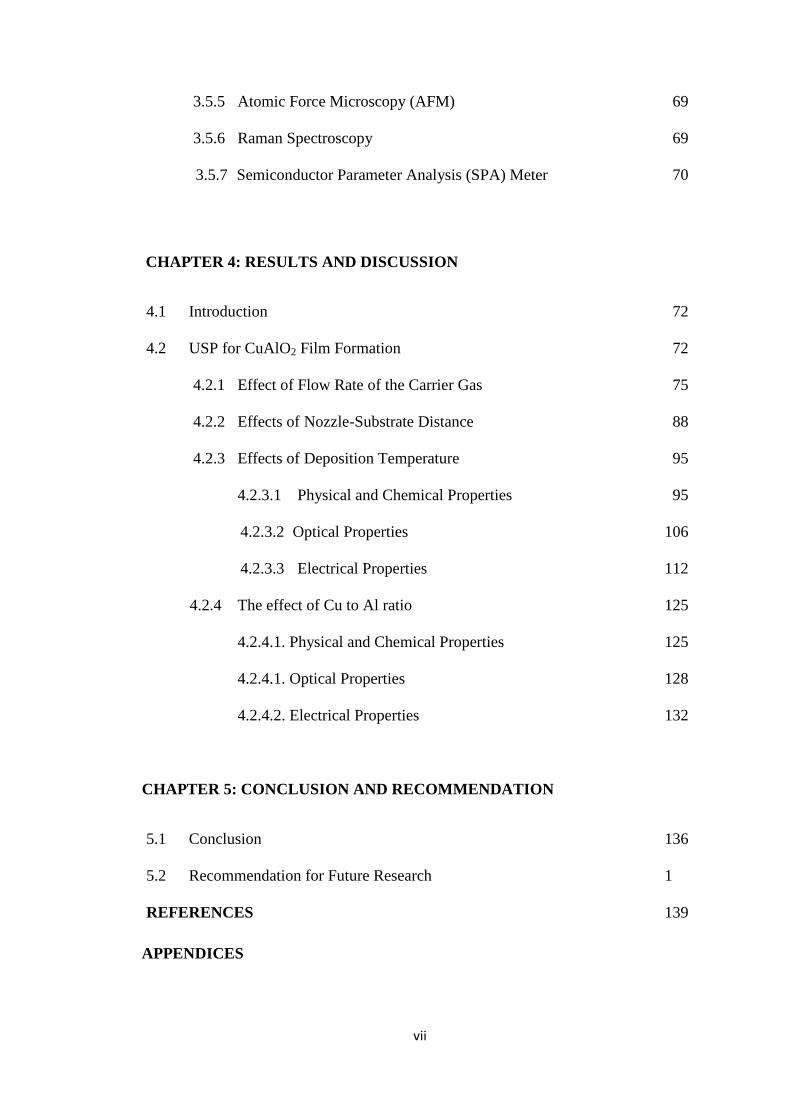
CHAPTER 4: RESULTS AND DISCUSSION
4.1 Introduction 72
4.2 USP for CuAlO2 Film Formation 72
4.2.1 Effect of Flow Rate of the Carrier Gas 75
4.2.2 Effects of Nozzle-Substrate Distance 88
4.2.3 Effects of Deposition Temperature 95
4.2.3.1 Physical and Chemical Properties 95
4.2.3.2 Optical Properties 106
4.2.3.3 Electrical Properties 112
4.2.4 The effect of Cu to Al ratio 125
4.2.4.1. Physical and Chemical Properties 125
4.2.4.1. Optical Properties 128
4.2.4.2. Electrical Properties 132
CHAPTER 5: CONCLUSION AND RECOMMENDATION
5.1 Conclusion 136
5.2 Recommendation for Future Research 1
REFERENCES 139
APPENDICES
viii
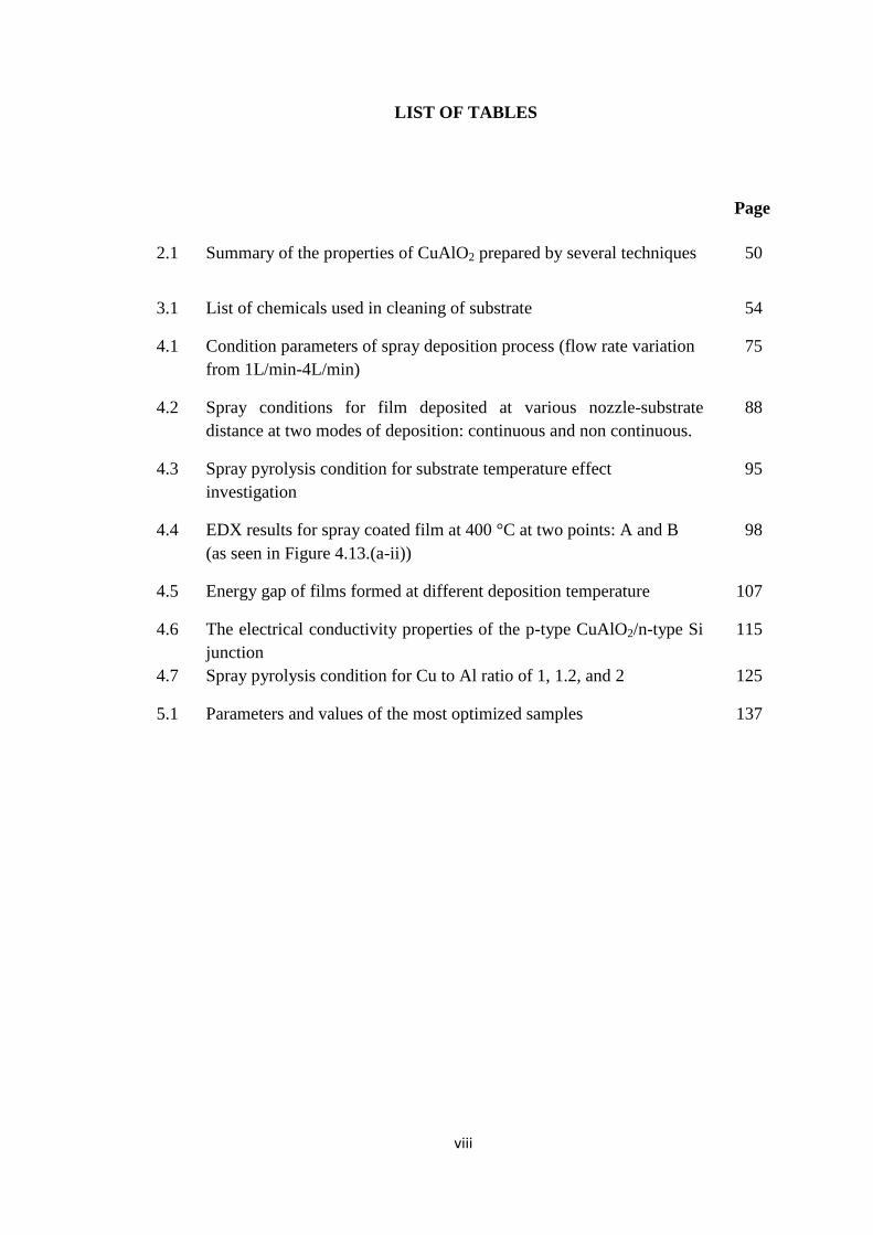
LIST OF TABLES
Page
2.1 Summary of the properties of CuAlO2 prepared by several techniques 50
3.1 List of chemicals used in cleaning of substrate 54
4.1 Condition parameters of spray deposition process (flow rate variation
from 1L/min-4L/min)
75
4.2 Spray conditions for film deposited at various nozzle-substrate
distance at two modes of deposition: continuous and non continuous.
88
4.3 Spray pyrolysis condition for substrate temperature effect
investigation
95
4.4 EDX results for spray coated film at 400 °C at two points: A and B
(as seen in Figure 4.13.(a-ii))
98
4.5 Energy gap of films formed at different deposition temperature 107
4.6 The electrical conductivity properties of the p-type CuAlO2/n-type Si
junction
115
4.7 Spray pyrolysis condition for Cu to Al ratio of 1, 1.2, and 2 125
5.1 Parameters and values of the most optimized samples
137

ix
LIST OF FIGURES
Page
2.1 A schematic band gap energy levels of a typical Transparent
Conducting Oxide (TCO)
8
2.2 P-type of transparent conducting oxides that have been produced at
the present
12
2.3 The schematic of diagram band which show the chemical
interaction between oxide ion and cation with d-close shell
electronic configuration
13
2.4 Atomic structure of AB2O4 spinel showing the position of A and B
atoms around oxygen
14
2.5 Crystal structure of Cu2O (i) and Cu2SrO2 (ii) 16
2.6 The concept of delafossite structures of 3R with the sequences of
stacking AaBbCcAa along c-axis. For hexagonal 2H polytype, the
stacking layer order is AaBbAb. The polyhedron and sphere
represent BO6 distorted octahedron and linearly coordinated A+
cations
18
2.7 Schematic representation of CuAlO2 at stoichiometric equilibrium
state (a), nonstoichiometric state with surplus oxygen in the lattice
site (b), and (c) nonstoichiometric state with excess oxygen in the
interstitial site
20
2.8 The crystal structure of CuAlO2. The layers of AlO6 and Cu are
alternately stacked along c-axis
22
2.9 TG-DTA evaluation of CuAlO2 24
2.10 Thermodynamic stability of CuO-Al2O3-CuAlO2 system at 0.21atm
oxygen pressure
25
2.11 Band diagram of p-CuAlO2+x/ n-Zn1-xAlxO 30
2.12 I-V characterization p-type CuAlO2/ n-ype Si 31
2.13 Energy band diagram of p type and n-type semiconductor before
contact, during contact and at equilibrium
32
x
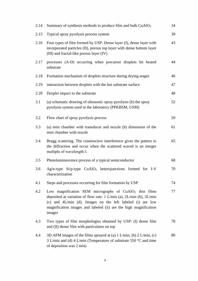
2.14 Summary of synthesis methods to produce film and bulk CuAlO2 34
2.15 Typical spray pyrolysis process system 39
2.16 Four types of film formed by USP: Dense layer (I), dense layer with
incorporated particles (II), porous top layer with dense bottom layer
(III) and fractal-like porous layer (IV)
43
2.17 processes (A-D) occurring when precursor droplets hit heated
substrate
44
2.18 Formation mechanism of droplets structure during drying stages 46
2.19 interaction between droplets with the hot substrate surface 47
2.20 Droplet impact to the substrate 48
3.1 (a) schematic drawing of ultrasonic spray pyrolysis (b) the spray
pyrolysis system used in the laboratory (PPKBSM, USM)
52
3.2 Flow chart of spray pyrolysis process 59
3.3 (a) mist chamber with transducer and nozzle (b) dimension of the
mist chamber with nozzle
61
3.4 Bragg scattering. The constructive interference gives the pattern to
the diffraction and occur when the scattered waved is an integer
multiple of wavelength λ
65
3.5 Photoluminescence process of a typical semiconductor 68
3.6 Ag/n-type Si/p-type CuAlO2 heterojunctions formed for I-V
characterization
70
4.1 Steps and processes occurring for film formation by USP 74
4.2 Low magnification SEM micrographs of CuAlO2 thin films
deposited at variation of flow rate: 1 L/min (a), 2L/min (b), 3L/min
(c) and 4L/min (d). Images on the left labeled (i) are low
magnification images and labeled (ii) are the high magnification
images
77
4.3 Two types of film morphologies obtained by USP: (I) dense film
and (II) dense film with particulates on top
78
4.4 3D AFM images of the films sprayed at (a) 1 L/min, (b) 2 L/min, (c)
3 L/min and (d) 4 L/min (Temperature of substrate 550 ºC and time
of deposition was 2 min)
80

xi
4.5 Roughness parameter of spray coated films at 1L/min to 4 L/min 81
4.6 The EDX characterization for sprayed coated film deposited at
carrier gas flow: (a) 1 L/min and (b) 4 L/min.
82
4.7 Images of droplets (a) and illustration of the characteristic of
droplets (b) flow leaving the nozzle to the substrate at four different
flow rates
84
4.8 Five possibilities on the characteristic of droplets when colliding to
the heated Si substrate
87
4.9 The SEM micrographs of CuAlO2 thin films deposited at nozzle-
substrate distance: 1 cm (a-i), 2 cm (b-i) and 3 cm (c-i) for samples
prepared using non continuous spray and 1 cm (a-ii), 2 cm (b-ii) and
3 cm (c-ii) for pulsed continuous
90
4.10 Schematic of decomposition processes of droplets at three different
nozzle-substrate distances
91
4.11 XRD pattern for films formed different nozzle-substrate distance, d
of 1 cm, 2 cm and 3 cm for non continuous mode
93
4.12 SEM micrographs at low and high magnification of CAO thin films
deposited at temperature: 400°C (a-i) and (a-ii), 450°C (b-i) and (b-
ii), 500°C (c-i) and (c-ii), 550°C (d-i) and (d-ii), and 600°C (e-i) and
(e-ii)
97
4.13 Cross section of CuAlO2 deposited on Si substrate formed at
temperature 550 °C
100
4.14 XRD characterization of CAO films deposited at various
temperatures from 400ºC to 600ºC
101
4.15 Temperature dependent Raman spectra of CAO film deposited in
the temperature range 450°C to 600°C
103
4.16 Normal mode parallel to hexagonal c-axis in the CuAlO2 104
4.17 Tauc plots for samples sprayed at different substrate‘s temperature:
400 °C (a), 450 °C (b), 500 °C (c), 550 °C (d) and 600 °C (e)
106
4.18 Adsorption coefficient of spray coated CuAlO2 films at temperature:
400°C (a), 450°C (b), 500°C (c), 550°C (d) and 600°C (e)
108
4.19 Photoluminescence spectrum of CuAlO2 thin film spray coated at
550°C
110
4.20 Optical transmission of spray coated CuAlO2 film grown at 550°C 112

xii
4.21 J-V curve of CuAlO2/Si at dark condition for sample made at
different substrate‘s temperature
113
4.22 The turn on voltage p-type CuAlO2/n-type Si 114
4.23 J-V characteristic of photodiode p-type CuAlO2/n-type Si under
illumination of light with power varied from 25 Watt to 100 Watt
for films deposited at: 400°C (a), 450°C (b), 500°C (c), 550°C (d)
and 600°C (d)
117
4.24 Photocurrent density substracted to current at dark condition of
spray coated CAO films in a junction with Si deposited at: 450°C
(a), 500 °C (b), 550°C (c) and 600°C
119
4.25 J-V characteristic of photodiode p-type CAO/n-type Si deposited at
550 °C
122
4.26 The J-V characteristic of the photodiode deposited at 550 °C for
dark condition and under the UV LED λ= 357 nm and P= 40 mW
122
4.27 The photodiode process in the pn junction layer 124
4.28 The XRD pattern of films deposited at three Cu to Al ratio of 1:1,
1.2:1, and 2:1
126
4.29 SEM micrographs of as grown CuAlO2 deposited at different Cu to
Al ratio: 1:1 (a), 1.2:1 (b), and 2:1 (c). The figures labeled with (i) is
low magnification SEM whilst the figures labeled (ii) on the right is
high magnification SEM
127
4.30 Tauc plot of the films with Cu to Al ratio of 1:1 (a), 1.2:1 (b), 2:1(c) 129
4.31 Absorption coefficient of CuAlO2 films with different Cu to Al ratio 131
4.32 J-V characteristic of the spray coated CuAlO2 films at dark
condition
132
4.33 The J-V curve of the n-Si/p-CuAlO2 under illumination for the film
with the ratio Cu to Al: 1 (a), 1.2 (b), 2 (c). The initial J-V
characterization is shown for the graph labeled with (-i-) on the left
column, and after subtracted to the dark current on the right column
labeled with (-ii-).
134
xiii
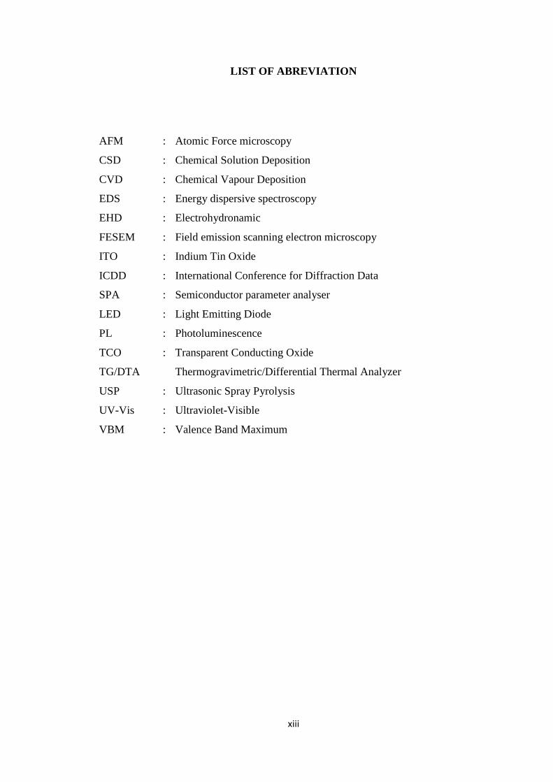
LIST OF ABREVIATION
AFM : Atomic Force microscopy
CSD
CVD
:
:
Chemical Solution Deposition
Chemical Vapour Deposition
EDS
EHD
:
:
Energy dispersive spectroscopy
Electrohydronamic
FESEM : Field emission scanning electron microscopy
ITO : Indium Tin Oxide
ICDD : International Conference for Diffraction Data
SPA : Semiconductor parameter analyser
LED : Light Emitting Diode
PL : Photoluminescence
TCO
TG/DTA
: Transparent Conducting Oxide
Thermogravimetric/Differential Thermal Analyzer
USP : Ultrasonic Spray Pyrolysis
UV-Vis : Ultraviolet-Visible
VBM : Valence Band Maximum

xiv
LIST OF SYMBOLS
A
%A
Fg
Fe
Fs
h
:
:
:
:
:
:
Surface Area (cm2)
Absorption
Gravitation Force (Kgms-2
)
Electrical Force (Coulomb)
Stokes Force (N)
Planck constant (eV.s)
I : Current (A)
I
G
l
N
µ
R
%R
S
T
t
ρ
σ
ʋ
:
:
:
:
:
:
:
:
:
:
:
:
:
Intensity (Lux)
Free Gibs Energy
Length (m)
Number of Particles
Mobility (cm2V
-1s
-1)
Resistance (Ω)
Reflectance
Enthalpy (Joule)
Temperature (°C)
Thickness (cm)
Resistivity (Ωm)
Conductivity (Sm-1
)
Frequency (Hz)

xv
LIST OF PUBLICATIONS
1. Iping Suhariadi, Zainovia Lockman, Sabar D Hutagalung, Kamsul Abraha,
Atsunori Matsuda. (2010) The formation of CuAlO2 thin films by nitrate route
chemical solution deposition method. Proceeding. The 3rd
Regional Conference
Interdisciplinary on Natural Resources and Material Engineering. October 2010.
Malaysia
2. Iping Suhariadi, Zainovia Lockman, Sabar D Hutagalung, Kamsul Abraha,
Atsunori Matsuda. (2010). Formation of CuAlO2 Thin Films by Ultrasonic
Spray Pyrolysis. Submitted to IOP Conference Series: Materials Science and
Engineering and accepted on 29 May 2011.
3. Iping Suhariadi, Zainovia Lockman, Sabar D Hutagalung, Kamsul Abraha,
Atsunori Matsuda. (2011) Formation of CuAlO2 Films by Ultrasonic Spray
Pyrolysis. Proceeding. The 1st International Conference on Materials
Engineering and 3rd
Regional Conference on Materials. February 2011.
Indonesia

xvi
PEMBENTUKAN FILEM NIPIS CuAlO2 MELALUI TEKNIK
PIROLISIS SEMBURAN UNTUK APLIKASI FOTODIOD
ABSTRAK
CuAlO2 merupakan oksida jenis –p yang lutsinar. Apabila digabungkan dengan bahan
jenis n, simpang p-n akan terbentuk dan boleh digunakan di dalam pelbagai aplikasi
menarik optik dan elektronik. CuAlO2 filem yang sekata, bebas daripada retakan dan
homogen telah dihasilkan melalui proses pemendapan cecair kimia melalui teknik
pirolisis semburan ultrasonik di atas substrat silicon jenis n yang telah dibersihkan.
Prapenanda cecair yang digunakan adalah campuran Cu(NO3)23H2O dan
Al(NO3)39H2O. Parameter pemendapan yang mempengaruhi sifat-sifat filem adalah
kadar aliran gas pembawa, jarak muncung-substrat, suhu substrat dan nisbah Cu
kepada Al telah dikaji. Parameter yang optimum telah diperolehi untuk pemendapan
filem: kadar aliran gas, 1 L/min, jarak muncung-substrate, 3 cm, suhu substrat 550 °C
dan nisbah Cu kepada Al adalah 1.2:1. Aliran titisan daripada kebuk melalui muncung
adalah laminar pada jarak dan kadar aliran gas pembawa ini. Pembentukan filem
dicadangkan melalui tindakbalas pirolitik antara ion-ion Cu dan ion-ion Al di dalam
setiap titisan apabila menghentam substrat yang panas. Imej SEM untuk sample yang
optima memnunjukkan filem terhasil mempunyai butiran dengan ketebalan ~1.9 µm.
Spektroskop UV-Vis telah menunjukkan filem terhasil mempunyai jurang tenaga
3.54eV dan kelutsinaran melebihi 60 % dalam julat cahaya nampak. Kekonduksian
filem adalah 0.354 Scm-1
. Filem menujukkan sifat diod apabila simpang-p CuAlO2/-n
Si dihasilkan dengan aliran voltan sekitar 0.4 V. Di bawah iluminasi cahaya nampak
yang berlainan kuasa, diod menujukkan sifat-sifat kesan fotoelektrik.

xvii
FORMATION OF CuAlO2 THIN FILMS BY ULTRASONIC SPRAY
PYROLYSIS FOR PHOTODIODE APPLICATIONS
ABSTRACT
CuAlO2 is a p-type oxide which is transparent. When coupled with an n-type
material, a p-n junction can be created and can be used in many interesting optical and
electronic applications. Smooth, crack free and homogenous CuAlO2 film was
produced by chemical solution deposition process via ultrasonic spray pyrolysis (USP)
technique on a cleaned n-type Si substrate. The precursor solution used was comprised
of a mixture of Cu(NO3)2.3H2O and Al(NO3)3.9H2O. The deposition parameter
influences the film properties are the flow rate of carrier gas, nozzle-substrate distance,
substrate‘s temperature and Cu to Al ratio was studied thoroughly. The optimum
parameters were found for the films deposited at a flow rate of 1 L/min, nozzle-
substrate distance of 3 cm, substrate‘s temperature of 550°C and Cu to Al ratio of
1.2:1. The flow was seen to be laminar at this distance and flow rate of carrier gas. The
formation of films was proposed to be due to the pyrolytic reaction of Cu and Al ions
in the droplets when the droplets impinged on the heated substrate. SEM images of the
most optimum sample is consisted of uniform grains with film thickness of ~1.9 µm.
UV-Vis spectroscopy revealed that the film have energy gap of 3.54 eV with
transparency above 60 % at visible light range. The conductivity of the film was 0.354
Scm-1
. The film showed the rectifying nature of diode in a junction of p-type
CuAlO2/n-type Si with turn on voltage around 0.4 eV. Under various illumination of
incandescent lamp, the diode showed photoelectric effect.
1
CHAPTER I
INTRODUCTION
1.1. Introduction
Transparent conducting oxides (TCOs) are a class of materials which have
attracted enormous attention from researchers and scientists all over the world. This
material offer unprecedented range of applications for many exciting devices that
requires both transparency and conductivity properties. Examples are to be used in
devices like photovoltaic (Beyer et al., 2007), flat panel displays (Lee et al., 1997), and
in light emitting and detecting photodiode (Kovac et al., 2003).
As the name signifies, TCOs are materials which are transparent and electrically
conducting. Finding a material with both properties is very challenging since highly
conductive material tends to be metallic whilst high transparent material is often an
insulator. However, several ceramic metal oxides are found to have a combination of
being conductive yet transparent. TCOs which are widely used now are the n-types like
In2O3:Sn, SnO2, Cd2SnO4 andAl:ZnO (Banarjee et al., 2003 and Choi et al., 2007). P
type TCOs have also been reported especially those that are based on cuprate oxides. P-
type, transparent delafossite CuAlO2 was first reported by Kawazoe et al., (1997). With
the discovery of this CuAlO2, the realization of transparent p-n junctions for the creation
of transparent semiconducting devices will be possible.
2
Apart from cuprate based oxides, there are not many transparent oxides which
are reported to be hole conducting and at the same time transparent. In most oxides,
electronegativity of oxygen 2p orbitals lead to the formation of deep valence band
maximum (VBM) therefore hole are localized around the oxygen atom. Moreover hole
doping is rather difficult as well. To overcome the strong localization, Kawazoe et al.,
(1997) suggested on the modification of the energy band structures of several metal
oxides to reduce the deep hole traps due to oxygen. This can be done by introducing
cationic elements which have d10
closed shell with energy comparable to the oxygen 2p
level. The closed d shell is also preferred to be used due to the coloration of open d shell
which may induce the transparency of the films (Buljan et al., 2001). There are several
metal oxides that can be created following this band modification model. The oxides are
centered on the cuprate based with CuAlO2 as leading candidate. To date CuAlO2 films
have been made by various methods: physical and chemicals. The formation of film at
low temperature using chemical methods is desired. Low temperature process is desired
as it will widen the choice (even on polymer), reduce interface reaction and cost
effective.
1.2. Problem Statement
Since Kawazoe et al. discovered p type conduction in CuAlO2, several studies on
the stoichiometry and preparation techniques of a single crystalline CuAlO2 have been
made. Evaluation on the thermodynamics and kinetic stability of CuAlO2 by solid state
reaction of CuO and α-Al2O3 annealed in air at 1200 °C shows the presence of CuAlO2

3
(Kumekawa et al., 2009). And, at lower temperatures, CuO and CuAl2O4 co-exist (Shy
and Tseng., 2005). The existence of CuAl2O4 has also been reported in sol-gel derived
film using nitrate precursor after been annealed at 800 ºC (Salavati-Niasari et al., 2009).
CuAl2O4 and CuO are said to be stable at 625°C to 1100°C (Jacob and Alcock., 1975).
And CuAlO2 only can be formed at 1050-1200°C. At elevated temperature >1200°C the
stable CuAlO2 may decompose (Kumekawa et al., 2009). There is only exist a small
window at which CuAlO2 can be formed. High deposition temperature limits the use and
choice of substrate. Amorphous CuAlO2 can be prepared by sputtering and the
properties of the amorphous film are generally acceptable: transparency above 75 % in
the visible region but with energy band gap of 1.6 eV. The room temperature electrical
conductivity of the CuAlO2 film is 0.32 Scm-1
(Chattopadhyay et al., 2007). Amorphous
CuAlO2 can be formed at much lower temperature.
Chemical spray deposition (CSD) process (CSD) is a versatile technique to form
CuAlO2 film on various substrates. CSD process can be done via spin coating, dip
coating, and spray coating to produce the thin film. Spray coating can be done by spray
pyrolysis technique. It has advantages over any physical methods are in term of
simplicity and cost effectiveness. The operation of equipment is easy enough and
applicable to extensive variety of precursor and substrate (Rim et al., 2002). In 2005,
Bouzidi et al., (2005) had successfully produced a thin film CuAlO2 by ultrasonic spray
pyrolysis (USP) using chloride precursors on a glass substrate at substrate‘s temperature
in the range of 450 to 525 °C. The amorphous CuAlO2 films were transformed to
crystalline CuAlO2 after annealing at 570 °C. The films had band gap energy reported in
4
the range of 3.34 to 3.87 eV (Bouzidi et al., 2005). It is known that there are several
parameters in the USP which will determine the final properties of the film produced.
One of them is the acidity level of the starting precursor. This effect of pH was studied
and reported by Singh et al., (2008) by varying the concentration of the HCl in the
chloride precursors the pH was altered. Nonetheless the films produced were not very
smooth, in fact were very inhomogenous (Singh et al., 2008). Chloride precursor may
not be the best of precursor to form smooth CuAlO2 film. The inhomogenity could be
due to the presence of Cl2 gas formed during the spray coating process. Prior to the
report by Singh et al, Toonoka et al., (2002) investigated on the effect of chloride,
alkoxide, nitrate and a mixture of these precursors to the properties of CuAlO2 film
made by CSD via dip coating. They reported on the superiority properties of the films
produced by using nitrate precursor as nitrate derived films were much more crystalline,
smoother and has better conductivity. To date, no work has been reported on the use of
nitrate precursor for CuAlO2 film formed by USP. Therefore, it is of interest to study the
quality of films formed by USP via nitrate route.
In this work, CuAlO2 thin films were produced by USP using nitrate precursors
(nitrate route) on silicon. As mentioned nitrate precursors were used due to their
advantages over the chlorides such as less aggressive and corrosive hence film formed
may have much better homogenity (Perednis., 2003). The deposition parameters were
investigated aiming at the formation of coating with desired phase at lower temperature.
Lower temperature process can be achieved by USP as the process occurs by ionic
reactions within droplets. Having achieved an optimum CuAlO2 films, the properties

5
especially the diode properties were studied. To date, not much have been reported on
the diode properties of CuAlO2 film. In this thesis, photodiode properties of transparent
CuAlO2 film on n-type silicon are presented.
1.3. Objective of the Research
The main objectives of this research are:
1. To produce CuAlO2 films at lower temperature by USP using nitrate precursor.
2. To investigate the effect of the deposition parameters to the properties of the
films especially the morphology, optical and electrical properties.
3. To characterize the diode properties of the CuAlO2 films formed by USP on n-
type Si especially under illumination.
1.4. Scope of Study
The study encompasses on the formation of p-type CuAlO2 thin films at lower
temperature by USP technique on an n-type (100) Si. The precursor was Cu and Al
nitrate salts were dissolved in appropriate solvents. The deposition parameters were
explored as to get an optimum condition to produce CuAlO2 film with good coverage
uniformity, and crystalline.
In this work X-Ray Diffraction (XRD) and Raman Spectroscopy were used to
characterize the phase present. Scanning Electron Microscopy (SEM) and Atomic Force

6
Microscopy (AFM) were used to characterize the surface morphology of the films.
Ultraviolet/Visible Spectroscopy (UV-Vis) and Photoluminescence (PL) were used to
characterize the optical properties of the films. To assess the diode properties of the
films on silicon, Semiconductor Parameter Analysis (SPA) was used under illumination.
Series of experiments were also done to characterize the photo response of the CuAlO2
on silicon.
1.5. Thesis Structure
This thesis consists of five chapters. The first chapter is on the background,
problem statement, research objectives, and the scope of this study. The second chapter
is on the literature review related to the research. The third chapter provides the detailed
methodology of this research. The fourth chapter presents the analysis and discussion of
the research findings. The fifth chapter provides the conclusion and suggestions for
future work.
7
CHAPTER 2
LITERATURE REVIEW
2.1. Introduction
Transparent Conducting Oxides (TCOs) have attracted vast attention across the
world due to its tremendous applications in realizing transparent electronics circuit for
the formation of transparent devices (Ohta and Hosono, 2004). The two special features
that must be accomplished in TCOs are wide energy gap (band gap) between the
material‘s conduction and valence band and high concentration and mobility of the
electrical carriers. Figure 2.1 represents an oversimplified energy band diagram of a
typical TCO. The band gap energy between the valence band and the conduction band
must be considerably bigger than the incoming energy of the visible light (photon). If the
material exhibit this, visible photon will only pass through the material without any
adsorption of the energy. The band gap of TCOs has to be greater than 3.1 eV to allow
light with energy of 2-3 eV (visible red to blue light) to pass through the material
(Thomas, 1997) .
However, highly transparent material is always associated with being insulating
with high electrical resistance. To create a material with high electrical conductivity,
free electrons are needed in the conduction band or free holes in the valence band. Free
electron can be created by excitation of electrons from the valence band to the
conduction band. But as mentioned, TCOs must have high energy gap and this limits the

8
generation or the excitation process by photon absorption. Generation due to heat energy
is possible to excite electrons in the conduction band.
Figure 2.1: A schematic band energy levels of a typical Transparent Conducting Oxide
(TCO) (Thomas, 1997)
Equation 2.1 shows the relationship of conductivity, σ with the number of free
electron, N, and the mobility µ of an electron. Based on this equation, σ can be increased
when N and µ are increased. N depends on the excitation process and is band gap
dependent.
σ = Nµe (2.1)
Therefore, to reduce resistivity the carrier mobility of the carrier charge must be
increased if N cannot be increased too much. As mentioned, TCOs are oxide
semiconductors. The conductivity is dependent on either p or n. To get transparency, the
9
band gap must be > 3 eV as to allow photons with λ= 300-500 nm to transmit.
Resistivity is often ρ < 10-3
Ωcm, with degenerate carrier density ≥ 1020
cm-3
and the hall
mobility µ ≥ 62.5 cm2V
-1s
-1 (Calnan and Tiwari, 2010). Generation of electron or hole is
dependent on intrinsic nature of the semiconductor as well. The µ is dependent on the
scattering events in the semiconductor and is largely dependent on the morphology,
crystallinity and impurities.
2.2. Transparent Conducting Oxides (TCOs)
2.2.1. N-Type Semiconductor
There are several n-type TCOs materials that have been used in electronic
industries. They are often used as transparent electrode for optoelectronic devices. N-
type TCOs have resistivity of < 10-4
Ω cm and overall transmittance of above 80 % at
the visible photon range. Several n-type TCOs have been successfully synthesized with
resitivity below 1.6 x 10⁻⁴
Ωcm, for example Al-doped ZnO (Al:ZnO) thin films
deposited by pulsed laser deposition (PLD) technique (Agura, 2003). Al:ZnO produced
by sputtering technique on the other hand has been reported to have resistivity of 1.39 x
10-4
Ωcm (Cao et al., 2004).
Indium tin oxide (ITO) [In2O3 : Sn) is perhaps the most used n-type TCO. ITO
deposited by PLD on a glass substrate has a reported resistivity value of 0.9 x 10⁻⁴
Ωcm
(Choi et al., 2003). ITO can also be sputtered to produce film with resistivity of ~ 10-4
Ωcm (Ray et al., 2007). However, it is believed that a shortage of indium may occur in

10
the near future. Moreover, the price of indium has increased drastically, thus indium free
TCOs are being sought after (Minami, 2008). Moreover, indium is toxic and hence is
harmful to human. Al:ZnO can be used to replace ITO as TCO for electrodes. ZnO is a
material that can easily be obtained or synthesized.
Another well known n-type material is fluorine doped indium oxide (F : In2O3 or
IFO). Thin IFO film has been reported to be produced by spray pyrolysis with resistance
of 120 Ωcm and transmittance of 88 % in the visible length (Rozati et al., 2004). IFO
has been reported by pyrosol method with good properties to be used as electrode for
solar cell (Untila et al., 2009).
Recently, new semiconductor materials consist of muticomponent oxides such as
ternary compounds have been produced. For example, spray coated MgIn2O4 film have
been reported to have electrical conductivity of 0.7 Scm-1
with overall transmittance of >
75 % at the visible photon range and also Hall mobility excess 1.5 x 10⁻³
cm2V
-1S
-1
(Sanjeeviraja et al., 2010). Excess Mg in MgIn2O4 have been reported to have resulted in
lowering the resistivity to 10-2
Ωcm (Lee et al., 2008). On the other hand, In4Sn3O12 film
deposited by sputtering has reported resistivity of 2 x 10⁻⁴
Ωcm, carrier concentration of
~ 1021
cm-3
, Hall mobility of 20 cm2V
-1s
-1 and average transmittance of > 80% in the
visible range (Minami et al., 1997).
The introduction of dopant metal to a conducting binary metal oxide is well
studied to achieve higher conductivity TCOs. Dopant causes disorder to the band
structure of the TCOs in which will cause localization of electron in the band structures
11
by introducing large number of carriers (Minami, 2005). But dopants are also scattering
center that may reduce µ in the TCOs.
2.2.2 P-Type Semiconductor
P-type semiconductor is characterized by the existence of acceptor level in the
band energy located close to the valence band that can induce hole formation. Holes are
the majority carriers responsible for the conduction mechanism of p-type materials.
Among the first p-type TCOs, Sato et al., (1993) reported on the NiO. However,
stoichiometric NiO exhibits an electrical resistivity in the order of 1013
Ωcm. Its
resistivity can be much lowered with the existance of nickel vacancies or interstitial
oxygen. Normally, p-type conductivity is of the order magnitude smaller than in the n-
type conductivity.
Apart from NiO, Cu2Oand CuO are among oxides exhibiting p-type
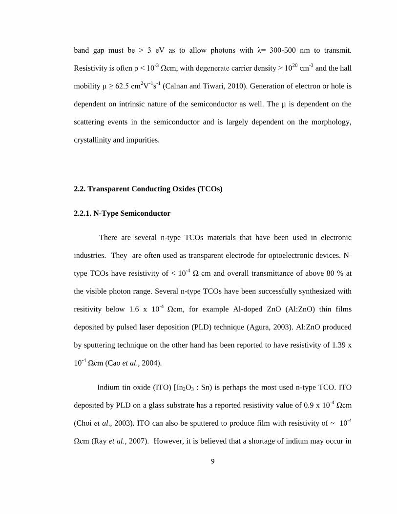
conductivity. Figure 2.2 shows p-type TCOs materials (Banarjee et al., 2008). This
figure displays all of the important hole conducting TCOs and will be explained in here.
12
Figure 2.2. P-type of transparent conducting oxides that have been produced at the
present (Banerjee et al, 2008).
It is best to first describe on the origin of the hole conductions in p-type TCO. As
mentioned, the conductivity in p-type TCOs is much less then n-type TCOs. One of the
reasons for high resistivity is on the lack of free holes available in p-type TCOs. Another
reason is the mobility of holes is known to be much smaller than that of electrons. The
lower conductivity of p-type is often attributed to the deep traps of highly
electronegative of oxygen atoms thus localizing the hole at the valence band edge of
oxide. As the holes are not delocalize, they are not free to move. To overcome this
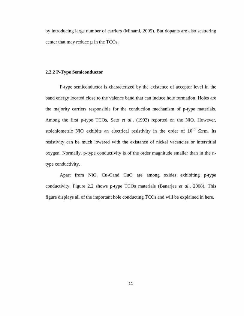
problem, cation with closed d-shell can be used to create a delocalization of the holes, as
shown in Figure 2.3 (Kawazoe et al., 2005).
13
Figure 2.3. The schematic of diagram band which show the chemical interaction
between oxide ion and cation with d-close shell electronic configuration (Kawazoe et al,
2005)
As seen in Figure 2.3, the localization from oxygen atom can significantly be
reduced by the modification of the cation with d10
closed from the metal such as Ag and
Cu. More dispersive bands with lower effective mass have been pushed up above the
non bonding O 2p or Cu 3d by the interaction of metal with some O 2p state (Sheng et
al., 2006).
Generally there are two main p-type TCOs, that are delafossite and non
delafossite oxides (Figure 2.2). The non delafossite TCOs are spinel and other types. In
the other types class, SrCu2O2, layered oxychalcogenide and binary oxide like NiO and
mixed oxide are listed. In spinel oxide, there are Ni based and Zn based.

14
2.2.2.1. Spinel Oxide
The group of material known as spinel has the general formula AB2O4 with A is
a divalent metal such as Mg, Mn, Cu, Zn, Cd, Pb, Co, Ni whereas B is a trivalent metal
such as Al, Cr, Fe, Co. The structure of the spinel is given in Figure 2.4. A atoms are
located at the point of a diamond type structure while the other atom are distributed
around them. Each of the A atom is surrounded by four equidistant, tetrahedrally
disposed oxygen atoms as shown in the Figure 2.4i. Meanwhile, for each B atom, around
them are six oxygen atom at the corner of octahedron shown in the Figure 2.4.ii. Each
oxygen atom is surrounded by three equidistant B atoms and one A atom.
Figure 2.4. Atomic structure of AB2O4 spinel showing the position of A and B atoms
around oxygen (Segev et al, 2005)
In the spinel structure, the atomic structure is not divided into AO and B2O3
groups or into A and BO2 ions. The whole crystal is a single molecule where each atom
15
is held by single bonds to those adjacent. Therefore, the empirical formula AB2O4 is the
only formula which correctly represent the structure of this substance (Huggins, 1923).
The spinel CuAl2O4 thin film can be deposited by sputtering. Post heat treatment
of the films increase their crystallinity. CuAl2O4 have been synthesized by sol-gel and
reported to have a band gap Eg value of = 2.10 eV (Salavati-Niasari et al., 2009). As
seen in Figure 2.2, the p-type TCOs can be spinel oxide, Ni based or Zn based.
Examples are NiB2O4 and ZnB2O4 respectively.
2.2.2.2. Non Delafossite : Cu2SrO2
SrCu2O2 has tetragonal crystal structure with lattice parameter of a=5.48Å and
c= 9.82 Å. The origin of p-type behavior in this material is resulted from +1 of Cu
cation. This material can be formed at considerably low temperature and has kinetics
stability (Varadarajan et al., 2005). Furthermore, SrCu2O2 is built up by Cu-O chain
along to the [100] and [010] direction in one dimensional, zigzag architecture with
θ=96.3 (Papadopoulou et al., 2008).
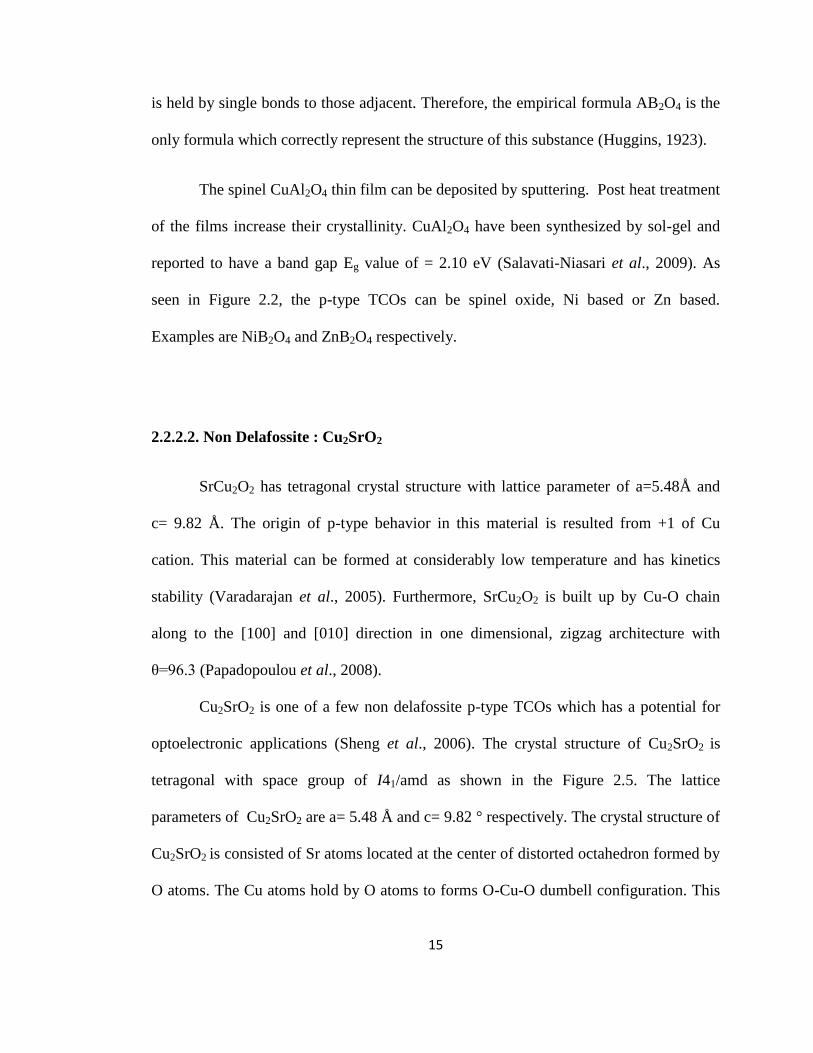
Cu2SrO2 is one of a few non delafossite p-type TCOs which has a potential for
optoelectronic applications (Sheng et al., 2006). The crystal structure of Cu2SrO2 is
tetragonal with space group of I41/amd as shown in the Figure 2.5. The lattice
parameters of Cu2SrO2 are a= 5.48 Å and c= 9.82 ° respectively. The crystal structure of
Cu2SrO2 is consisted of Sr atoms located at the center of distorted octahedron formed by
O atoms. The Cu atoms hold by O atoms to forms O-Cu-O dumbell configuration. This
16
dumbell may similar to Cu2O as shown in Figure 2.5 (i) therefore this Cu2SrO2 can be
considered to be derived from the Cu2O2. However the discrepancy of those dumbell
structure is in Cu2O the dumbell is built three dimensionally whilst in Cu2SrO2 the
dumbells arrangement is one dimensional zigzag chains along the c and b axis
orientation (Nie et al., 2002). Note that Cu2O is also p-type conducting.
Not many works on the synthesis of Cu2SrO2 have been reported so far.
However, in 2003 Roy et al reported on the deposition of Cu2SrO2 thin film by spraying
and PLD. The films deposited by spraying method have to be treated by post annealing
in order to obtain pure Cu2SrO2 phase whilst the film deposited using PLD has a mixture
of Cu2SrO2 with Cu2O (Roy et al., 2003). The improvement of Cu2SrO2 formation by
PLD was shown by Varadarajan et al., (2005) where they reported on the epitaxial
growth of nearly pure phase of Cu2SrO2 at 500°C. MOCVD derived Cu2SrO2 thin film
was also reported at temperature 480°C to 540°C. The as deposited film is consist of
Figure 2.5. Crystal structure of Cu2O (i) and Cu2SrO2 (ii)

17
mixture of CuO and SrCO3 (Deschanvres et al., 2008). Cu2SrO2 can only be synthesized
at low oxygen pressure.
2.2.2.3. Delafossite p-type TCO
Delafossite has hexagonal layered crystal structure with layers of AO2 and A
stacked alternately perpendicular to c-axis. The general formula of delafossite structure
is A+1
B3+
O2. As seen in Figure 2.6, delafossite consists of a rather distorted edge-shared
BO6 octahedra and closed packed A+ cation planes to form linear O-A
+1-O dumbbells.
The four cations that is one A+1
and three B3+
link the oxygen. Based on the stacking
layer structures, the possible polytype may coexist are rombohedral ―3R‖ which have
arrangement structures AaBbCcAa whilst the hexagonal ―2H‖ polytype consists of
sequence arrangement AaBbAa… (Ingram et al., 2004). Nonetheless, there are no
significant differences in the electrical properties between 2H and 3R since both had
almost the same α-axis (Deng et al., 2009).
As mentioned and seen in Figure 2.2, there two type of p-type TCOs with delafossite
structures: CuBIII
O2 and AgBIII
O2 where BIII
is trivalent cation. Ag based delafossite
oxides have large band gap of > 4.12 eV and transparency above 50 % (Vanaja et al.,
2008). However, the Ag based delafossite is much more difficult to produce and it is
unstable thermodynamically (Clayton et al., 2002). The Cu based will be explained in
the next sub heading.

18
Figure 2.6. The concept of delafossite structures of 3R with the sequences of stacking
AaBbCcAa along c-axis. For hexagonal 2H polytype, the stacking layer order is AaBbAb.
The polyhedron and sphere represent BO6 distorted octahedron and linearly coordinated A+
cations (Ingram et al., 2004 and Doumerc et al, 1987).
2.3. Delafossite p-type CuAlO2
CuIM
IIIO2 has gained much interest as p-type TCOs. Apart from delafossite
materials, Cu2O and CuO are known to have holes conduction as well. The first report
on the electrical conductivity of CuO is by Weichman where photoconductivity was
reported to depend on the oxygen content in the CuO (Weichman, 1960). The energy
band gap of CuO and Cu2O are in the range of 1.7 to 2.2 eV (Kose et al., 2008). The
small band gap value is one of the main reason underlay CuO and Cu2O are not being
considered as TCOs. These oxides are conducting but coloured. The small band gap of
Cu2O is assumed originate from the three dimensional interaction between electron 3d10
electron and neighboring Cu+
ions. The dumbbell unit in Cu2O connected three

19
dimensionally rather than connected preferentially parallel to c-axis with two
dimensional layers sandwiched by AlO6 octahedron similar to CuAlO2. This controls the
degree of mixing between O 2p and Cu 3d in the valence band vicinity. In Cu2O, four
Cu ion linked to each O ions. Thus, the interactions and mixing between O 2p and Cu 3d
is rather smaller than those in CuAlO2 and the valence band top of CuAlO2 has smaller
dispersion than Cu2O. As a result the mobility and narrow gap in Cu2O have been
observed (Yanagi et al., 2000). Moreover, the strong coloration effect as reported by
Richardson et al., (2001) which arise from the d10
—d10
interaction in this copper oxides
encourage many researchers to find more materials with larger band gap as to increase
transparency (Buljan et al., 2001).
P-type conductivity in delafossite oxides arise when there is a lack of metal
cations or excess in oxygen within the crystal lattice. Defect chemistry therefore plays
an important role in the determination of the final conductivity of the delafossite oxide
(Koumoto et al., 2001). Excess oxygen and Cu or Al deficient will create more holes as
written in (2.2).
O2(g) = 2Oox +VCu‘+VAl‘‘‘+4h
* (2.2)
In (2.2) VCu, Oo, VAl and h are Cu vacancy, oxygen in oxygen site, Al vacancy and
electron hole respectively. The superscript x, ‗,
* refer to effective charge state for
neutral, negative and positive of the vacancies and holes respectively. The presence of
excess oxygen in the delafossite film changes the equilibrium formula of the compound
which can be rewritten as CuAlO2+x. As seen in (2.2), more oxygen creates more holes.
20
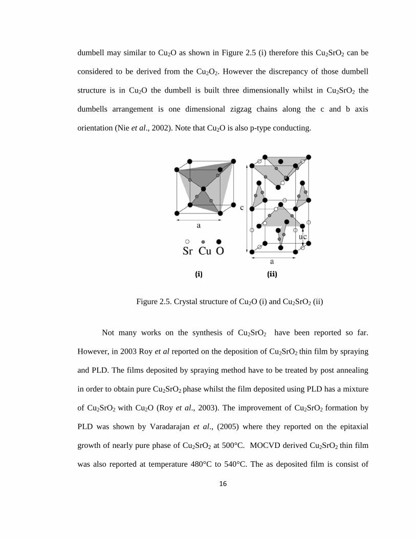
The schematic of excess oxygen in the lattice site and interstitial site in CuAlO2
delafossite compound is shown in Figure 2.7 (Banerjee and Chattopadhyay, 2005). In
this figure, (a) shows stoichiometric CuAlO2 whereas (b) and (c) shows excess oxygen
at different sites.
Figure 2.7. Schematic representation of CuAlO2 at stoichiometric equilibrium state (a),
nonstoichiometric state with surplus oxygen in the lattice site (b), and (c) nonstoichiometric state
with excess oxygen in the interstitial site (Banerjee and Chattopadhyay, 2005)

21
According to Kawazoe et al., (1997) most metal oxides have strong localization
at the upper edge of the valence band hence no free carriers exist. The modification of
the energy band structure is therefore needed as to reduce the localization and to free
more carriers. To do this, the cationic species must possess a closed shell with energy
comparable to the energy of the 2p levels of the oxygen anion. The Cu+ has an electronic
configuration of d10
s0 where the energy of d
10 closed shell will overlap to that 2p
electron from the oxygen ions. The crystal structure is an important factor to be
considered as well.
Tetrahedral coordination is a suitable candidate as there is a lack of oxygen
bonding to the cation in the structure. This can further reducing the localization
behaviors of the 2p electrons of oxide ion. In addition, lowering the dimension of
crosslinking of Cu+ ions is required to widen the bandgap because of the direct
interaction between d10
electrons on neighbouring Cu+ ions will reduce the band gap. As
mentioned, energy gap > 3 eV must be achieved to get transparent oxide. Considering all
of these requirements, Kawazoe had proposed CuAlO2 delafossite structure one of the
potential candidates for high conductive p-type TCO (Kawazoe et al., 1997).
CuAlO2 has a rombohedral space group of R3m. In the structure, the Cu atoms
are linearly linked to the oxygen atom with 2 fold coordination. Oxygens are
coordinated 4-fold which comes from 3 fold by Al and 1-fold by Cu. Figure 2.8 shows
the crystal structure of CuAlO2 showing the layers of AlO6 and Cu alternately stacked
along c-axis.

22
Figure 2.8. The crystal structure of CuAlO2. The layers of AlO6 and Cu are alternately stacked
along c-axis (Tate et al., 2009).
2.4. CuAlO2: Phase Equilibria
As described previously, the emphasis on the p-type TCOs has been focused on
gaining understanding on what is the origin of the hole conduction and how increase the
conductivity. In this context, apart from crystal structure, micro structural and phase
purity of p-type TCOs must also be considered. A smooth, uniform CuAlO2 is desired to
avoid electron scattering and when used in optical application, light scattering is
expected in a rough oxide. Processing and formation of CuAlO2 as p-type TCO have
therefore been focused in achieving smooth, pure CuAlO2.
In here phase equilibria will be discussed as it is important to know on the conditions
at which CuAlO2 exist. Equations (2.3), (2.4), (2.5) and (2.6) for the formation of CuO,
CuAlO2 and CuAl2O4 (Jacob and Alcock., 1975).
23
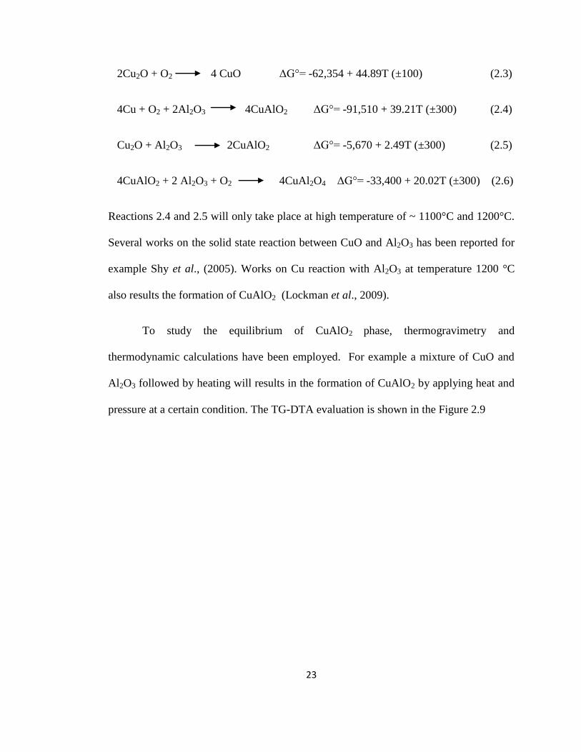
2Cu2O + O2 4 CuO ΔG°= -62,354 + 44.89T (±100) (2.3)
4Cu + O2 + 2Al2O3 4CuAlO2 ΔG°= -91,510 + 39.21T (±300) (2.4)
Cu2O + Al2O3 2CuAlO2 ΔG°= -5,670 + 2.49T (±300) (2.5)
4CuAlO2 + 2 Al2O3 + O2 4CuAl2O4 ΔG°= -33,400 + 20.02T (±300) (2.6)
Reactions 2.4 and 2.5 will only take place at high temperature of ~ 1100°C and 1200°C.
Several works on the solid state reaction between CuO and Al2O3 has been reported for
example Shy et al., (2005). Works on Cu reaction with Al2O3 at temperature 1200 °C
also results the formation of CuAlO2 (Lockman et al., 2009).
To study the equilibrium of CuAlO2 phase, thermogravimetry and
thermodynamic calculations have been employed. For example a mixture of CuO and
Al2O3 followed by heating will results in the formation of CuAlO2 by applying heat and
pressure at a certain condition. The TG-DTA evaluation is shown in the Figure 2.9
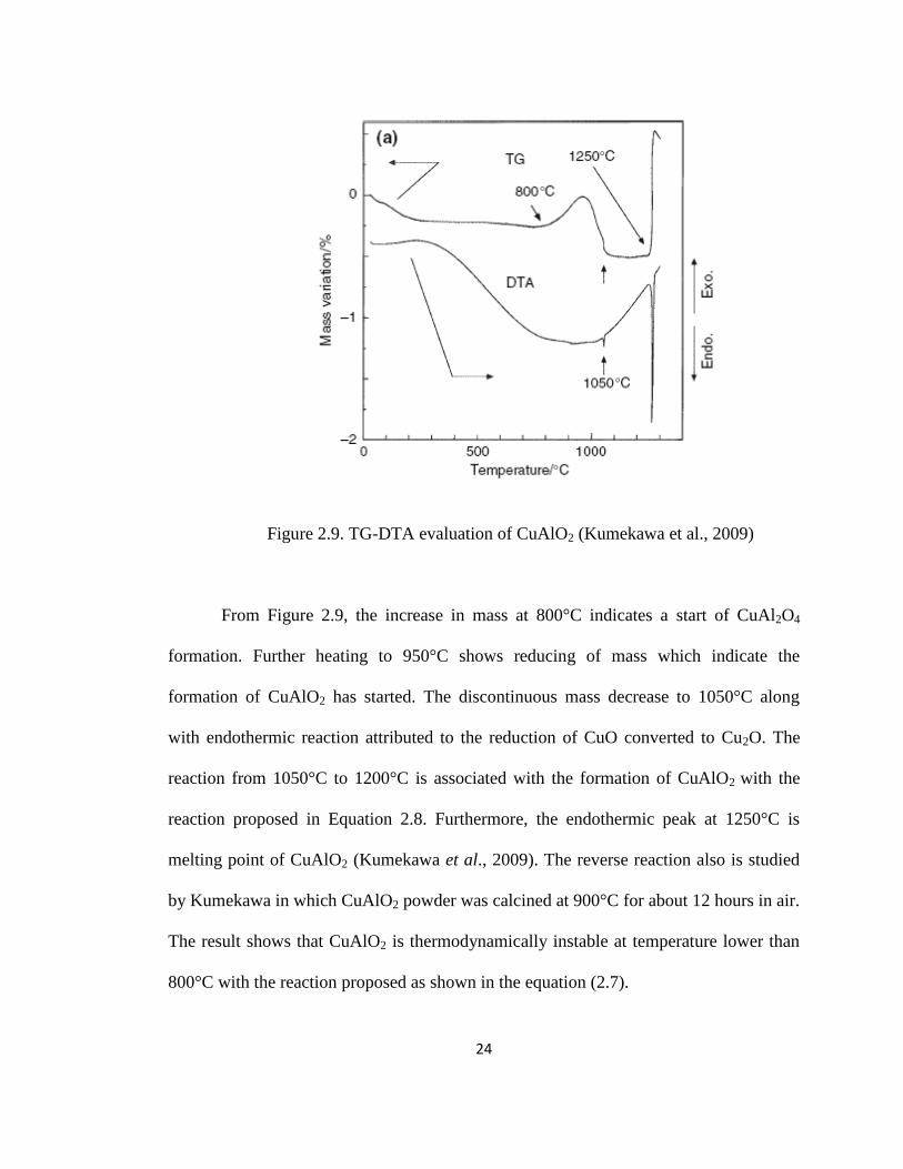
24
Figure 2.9. TG-DTA evaluation of CuAlO2 (Kumekawa et al., 2009)
From Figure 2.9, the increase in mass at 800°C indicates a start of CuAl2O4
formation. Further heating to 950°C shows reducing of mass which indicate the
formation of CuAlO2 has started. The discontinuous mass decrease to 1050°C along
with endothermic reaction attributed to the reduction of CuO converted to Cu2O. The
reaction from 1050°C to 1200°C is associated with the formation of CuAlO2 with the
reaction proposed in Equation 2.8. Furthermore, the endothermic peak at 1250°C is
melting point of CuAlO2 (Kumekawa et al., 2009). The reverse reaction also is studied
by Kumekawa in which CuAlO2 powder was calcined at 900°C for about 12 hours in air.
The result shows that CuAlO2 is thermodynamically instable at temperature lower than
800°C with the reaction proposed as shown in the equation (2.7).