Embed Size (px)
Citation preview

Revision: 1.0 912-3000-049May 27, 1998
OPTi®
FireLink
82C861 PCI-to-USB Bridge
Data Book

OPTi Inc.888 Tasman DriveMilpitas, CA 95035Tel: (408) 486-8000Fax: (408) 486-8001
WWW: http://www.opti.com/
ii
CopyrightCopyright © 1997, OPTi Inc. All rights reserved. No part of this publication may be reproduced, transmitted, tran-scribed, stored in a retrieval system, or translated into any language or computer language, in any form or by anymeans, electronic, mechanical, magnetic, optical, chemical, manual, or otherwise, without the prior written per-mission of OPTi Inc., 888 Tasman Drive, Milpitas, CA 95035.
DisclaimerOPTi Inc. makes no representations or warranties with respect to the design and documentation hereindescribed and especially disclaims any implied warranties of merchantability or fitness for any particular purpose.Further, OPTi Inc. reserves the right to revise the design and associated documentation and to make changesfrom time to time in the content without obligation of OPTi Inc. to notify any person of such revisions or changes.
TrademarksOPTi and OPTi Inc. are registered trademarks of OPTi Inc. All other trademarks and copyrights are the propertyof their respective holders.

FireLink
Table of Contents
OPTi®
912-2000-015 Page iiiRevision: 1.0
1.0 Features ............................................................................................................................ 1
2.0 Overview ........................................................................................................................... 1
2.1 Replacing CMD® USB0670/3 with OPTi’s 82C861 FireLink ............................................................2
2.2 Power Management Features ............................................................................................................2
2.2.1 Enabling CLKRUN#................................................................................................................3
2.2.2 Putting FireLink into Suspend State .......................................................................................3
3.0 Signal Definitions............................................................................................................. 4
3.1 Terminology/Nomenclature Conventions ........................................................................................4
3.2 Signal Descriptions ............................................................................................................................7
3.2.1 Clock and Reset Interface Signals .........................................................................................7
3.2.2 PCI Bus Interface Signals.......................................................................................................7
3.2.3 USB Interface Signals ............................................................................................................9
3.2.4 Legacy and Interrupt Interface Signals.................................................................................10
3.2.5 USB Power and Misc. Signals..............................................................................................10
3.2.6 Power and Ground Pins .......................................................................................................11
3.2.7 Firelink 82C861 Strapping Options.......................................................................................11
4.0 Functional Description .................................................................................................. 12
4.1 Universal Serial Bus (USB) ..............................................................................................................12
4.1.1 PCI Controller .......................................................................................................................13
4.1.2 Host Controller......................................................................................................................144.1.2.1 Legacy Support .....................................................................................................16
5.0 Register Descriptions .................................................................................................... 17
5.1 PCICFG Register Space ...................................................................................................................17
5.2 Host Controller Register Space.......................................................................................................21
FireLink
OPTi®
Table of Contents (cont.)
Page iv 912-2000-015Revision: 1.0
5.2.1 Legacy Support Registers ....................................................................................................31
6.0 Electrical Ratings........................................................................................................... 33
6.1 Absolute Maximum Ratings.............................................................................................................33
6.2 DC Characteristics: VCC = 3.3V or 5.0V ±5%, TA = 0°C to +70°C.................................................33
6.3 AC Characteristics (Preliminary).....................................................................................................34
6.3.1 PCI Bus AC Timings.............................................................................................................34
6.3.2 USB AC Timings: Full Speed Source ...................................................................................35
6.3.3 USB AC Timings: Low Speed Source ..................................................................................36
7.0 Mechanical Package Outlines....................................................................................... 38
8.0 NAND Tree Test Mode ................................................................................................... 40

FireLink
List of Figures
OPTi®
912-2000-015 Page vRevision: 1.0
Figure 2-1 FireLink Block Diagram ...................................................................................................................1Figure 3-1 LQFP Pin Diagram (Note) ...............................................................................................................5Figure 4-1 USB Functional Block Diagram .....................................................................................................12Figure 6-1 Setup Timing Waveform ................................................................................................................34Figure 6-2 Hold Timing Waveform ..................................................................................................................34Figure 6-3 Output Delay Timing Waveform.....................................................................................................34Figure 6-4 Differential Data Jitter ....................................................................................................................37Figure 6-5 Differential to EOP Transition Skew and EOP Width.....................................................................37Figure 6-6 Receiver Jitter Tolerance...............................................................................................................37Figure 7-1 100-Pin Low-Profile Quad Flat Pack (LQFP).................................................................................38Figure 7-2 100-Pin Quad Flat Pack (QFP)......................................................................................................39

FireLink
OPTi®
List of Figures (cont.)
Page vi 912-2000-015Revision: 1.0

FireLink
OPTi®
List of Tables
Page vii 912-2000-049Revision: 1.0
Table 2-1 Strapping Option Differences ..........................................................................................................2Table 3-1 Signal Definitions Legend................................................................................................................4Table 3-2 Numerical Pin Cross-Reference List ...............................................................................................6Table 4-1 PCI Controller Register Map..........................................................................................................13Table 4-2 Host Controller Register Map ........................................................................................................14Table 4-3 Legacy Support Register Map .......................................................................................................16Table 4-4 Emulated Registers and Side Effects ............................................................................................16Table 5-1 PCICFG 00h-FFh ..........................................................................................................................17Table 5-2 MEMOFST 00h-5Ch......................................................................................................................21Table 5-3 MEMOFST 100h-1Fh (Legacy Support Registers) .......................................................................31

FireLink
OPTi®
List of Tables (cont.)
Page viii 912-2000-015Revision: 1.0
82C861
FireLinkPCI-to-USB Bus Bridge
OPTi®
912-3000-049 Page 1Revision: 1.0
1.0 Features• Fully compatible with USB OHCI specification
• Controls two USB ports
• USB 1.1 compliant
• Pin compatibility with the CMD® USB0670/3 PCI-USB Controller
• Implements CLKRUN# pin to support low power portable applications
• Supports OPTi IRQ Driveback Cycle to improve pin utiliza-tion and increase interrupt selection flexibility
• Core operates at 5.0V or 3.3V and is controlled by strap or register
• Two package types available:- 100-pin LQFP (Low-profile Quad Flat Pack)- 100-pin QFP (Quad Flat Pack)
• Low cost solution: enabling factor in USB market
• Multiple operating system support- Windows 95 OSR2 with USB supplement
- Windows 98- Windows NT 5.0- Windows CE
2.0 OverviewThis document describes OPTi’s FireLink (82C861) PCI-to-USB Bus Bridge for Silicon Revision 1.0. It details:
• How FireLink can be used as a direct replacement for the CMD® USB0670.
• Power Management
• Signal Definitions
• Strap Selectable Options
• Register Descriptions
Figure 2-1 shows a block diagram of FireLink.
Figure 2-1 FireLink Block Diagram
CLKRUN#
CoreClock
ControlLogic
GlobalOperations
PCI ConfigPCI SlavePCI Master
PCI Bus
List Processor
USB SIE
BusMaster
Clock
Data Buffer
PCI Interface
Gen
Engine
Port2
PWRGD2PWRFLT2PWRON2VD2+VD2–
Port1
PWRGD1PWRFLT1PWRON1VD1+VD1–
Root HubControl
USB
PCI I/O Kybd Legacy
FrameManagement
1
USB2

FireLink
Page 2 912-3000-049Revision: 1.0
OPTi®
2.1 Replacing CMD® USB0670/3 with OPTi’s 82C861 FireLinkFireLink (82C861) is a direct, pin-compatible upgrade for the CMD® USB0670/3 USB Controller. Like the CMD® part, FireLinkimplements two independent USB ports. FireLink additionally offers the following features:
• CLKRUN# pin, which allows the host chipset to keep the part in a very low power state most of the time. Start-up latency from this state is negligible.
• Supports both 5V and 3.3V operation from the same core. The operational voltage is selected by a strap option and can be overridden by register.
Pinouts for OPTi’s 82C861 are congruent to CMD®’s USB0670/3. However, care must be taken to make sure that both thepolarity is set correctly for all the signals and that the strapping options for the 82C861 are set correctly when replacing theUSB0670/3.
Table 2-1 Strapping Option Differences
Operating Voltage OPTi's FireLink can replace either the 5V or the 3.3V CMD part. Selecting the operating voltage can be done in two ways: bystrapping the TEST0 pin or by writing to the PCI configuration register, PCICFG 52h[5].
Strapping TEST0 low causes FireLink to operate at 5V while strapping it high causes FireLink to operate at 3.3V.
Writing to the PCI configuration register overrides inputs to the TEST0 pin. Set PCICFG 52h[5] = 1 to operate FireLink at 5V.Set PCICFG 52h[5] = 0 to operate FireLink at 3.3V.
Over-current detectionPWRFLT1 and PWRFLT2 each detects over-current faults on its respective USB port. In the OPTi Firelink, the active polarity onPWRFLT1 and PWRFLT2 are strapable. For active high, strap the pins low and for active low, strap the pins high. On the CMDpart, the over-current detectors are active low. If FireLink replaces a CMD part, an external pull-up may be required to strap theFireLink to the correct polarity.
2.2 Power Management FeaturesFireLink revision 1.0 implements new power management features which can reduce the overall power consumed in mobileUSB applications. Several key features include the following:
• PCI clock can be stopped using CLKRUN# control
• 48MHz USB clock can be stopped when FireLink is put into suspend
• USB I/O cells can be turned off while in suspend
• The ability to wake the system up from a USB resume event by using CLKRUN#
2.2.1 Enabling CLKRUN#To enable FireLink to use CLKRUN# in a PCI system, the following PCI configuration registers need to be initialized to the fol-
Pin # CMD® 0670/3 OPTi Firelink Comment
10 PWRFLT1 PWRFLT1 OPTi: Active High or Low (strap)CMD®: Active Low
23 PWRFLT2 PWRFLT2 OPTi: Active High or Low (strap)CMD®: Active Low
25 TEST0 TEST0 Strap Option:CMD®: Low=OperationalOPTi: Low=5.0V Operation High=3.3V Operation
When operating at 3.3V, requires pull-up.

FireLink
912-2000-049 Page 3Revision: 1.0
OPTi®
lowing:
- PCICFG 50h[2] = 1 (enable CLKRUN# on host interface)
- PCICFG 50h[4] = 1 (enable power saving CLKRUN# mode)
2.2.2 Putting FireLink into Suspend StateBefore a host system goes into a suspend state, the operating system should put the OHCI USB controller into USB suspendmode by writing to OHCI register MEMOFST 04h[7:6] = 11. After FireLink is put into suspend in this manner, additional stepscan be taken to further reduce power consumption. One of these options is to stop the USB clock. If this route is taken, the USBclock must be stopped and started in a glitch free manner. Even though the USB clock is stopped, the system can be woken upby using CLKRUN# if it is enabled, which will be asserted on a USB wake up event (resume signaling, connect, disconnect).The USB I/O cells can also be disabled to reduce power by setting the PCI configuration register to the following value:
- PCICFG 50h[1:0] = 11
The I/O cells should be disabled by the BIOS before going into suspend, and re-enabled by the BIOS before giving control backto the operating system.

FireLink
Page 4 912-3000-049Revision: 1.0
OPTi®

FireLink
912-2000-049 Page 5Revision: 1.0
OPTi®
3.0 Signal Definitions
3.1 Terminology/Nomenclature ConventionsThe “#” symbol at the end of a signal name indicates that theactive, or asserted state occurs when the signal is at a lowvoltage level. When “#” is not present after the signal name,the signal is asserted when at the high voltage level.
The terms “assertion” and “negation” are used extensively.This is done to avoid confusion when working with a mixtureof “active low” and “active high” signals. The term “assert”, or“assertion” indicates that a signal is active, independent ofwhether that level is represented by a high or low voltage.The term “negate”, or “negation” indicates that a signal isinactive.
The tables in this section use several common abbreviations.Table 3-1 lists the mnemonics and their meanings. Note thatTTL/CMOS/Schmitt-trigger levels pertain to inputs only. Out-puts are driven at CMOS levels.
Table 3-1 Signal Definitions Legend
Mnemonic Description
Analog Analog-level compatible
CMOS CMOS-level compatible
Dcdr Decoder
Ext External
G Ground
I Input
Int Internal
I/O Input/Output
Mux Multiplexer
NIC No Internal Connection
O Output
OD Open drain
P Power
PD Pull-down resistor
PU Pull-up resistor
S Schmitt-trigger
S/T/S Sustain Tristate
TTL TTL-level compatible

FireLink
Page 6 912-3000-049Revision: 1.0
OPTi®
Figure 3-1 LQFP Pin Diagram (Note)
Note: Figure 3-1 shows a pin diagram of the 82C861 packaged in an LQFP (Low-profile Quad Flat Pack, square). The device is also available in a QFP (Quad Flat Pack, rectangular). The pin assignment remains the same.
Refer to Section 6.0, "Mechanical Package Outlines" for details regarding packaging.
123
4567
891011
12131415
16171819
20212223
2425
50494847464544434241403938373635343332313029282726
757473
72717069
68676665
64636261
60595857
56555453
5251
767778798081828384858687888990919293949596979899100
A20_outAD2AD1
AD0GND
USBCLKVCC
NICPWRON1PWRFLT1PWRGD1
VCC3VD1+VD1–GND
GNDVCC3VD2+VD2–
GNDTEST0
PWRGD2PWRFLT2
PWRON2TEST1
VC
C_I
SA
IRQ
1_ou
t
IRQ
12_o
utS
MI#
INT
A#
RE
SE
T#
PC
ICLK
GN
DV
CC
GN
T#
RE
Q#
AD
31A
D30
AD
29G
ND
VC
CA
D28
AD
27A
D26
AD
25C
LKR
UN
#
GN
DA
D24
C/B
E3#
IDS
EL
SERR#NICIRQ12_in
GNDPERR#STOP#DEVSEL#
TRDY#IRDY#GNDVCC
FRAME#C/BE2#AD16AD17
VCCGNDAD18AD19
AD20AD21GNDA20_in
AD22AD23
PA
RC
/BE
1#A
D15
AD
14G
ND
VC
CA
D13
AD
12A
D11
GN
DA
D10
AD
9A
D8
C/B
E0#
GN
D
NIC
VC
CA
D7
AD
6
AD
5G
ND
IRQ
1_in
VC
C
AD
4A
D3
82C861
FireLink
Key:
FireLink is a pin-compatible replacement for the CMD USB device, even though some ofFireLink’s pins are called out as NIC (No Internal Connection).
Pin 46 (CLKRUN#) can be a connected to VCC if FireLink is used in a CMD-based system.

FireLink
912-2000-049 Page 7Revision: 1.0
OPTi®
Table 3-2 Numerical Pin Cross-Reference List
PinNo. Signal Name Power Plane
1 A20_out
VCC
2 AD2
3 AD1
4 AD0
5 GND
6 USBCLK
7 VCC
8 NIC
9 PWRON1
10 PWRFLT1
11 PWRGD1
12 VCC3
VCC313 VD1+
14 VD1–
15 GND
16 GND VCC
17 VCC3
VCC318 VD2+
19 VD2–
20 GND
21 TEST0
VCC22 PWRGD2
23 PWRFLT2
24 PWRON2
25 TEST1
26 VCC_ISA
VCC_ISA27 IRQ1
28 IRQ12
29 SMI#
VCC
30 INTA#
31 RESET#
32 PCICLK
33 GND
34 VCC
35 GNT#
36 REQ#
37 AD31
38 AD30
39 AD29
40 GND
41 VCC
VCC
42 AD28
43 AD27
44 AD26
45 AD25
46 CLKRUN#
47 GND
48 AD24
49 C/BE3#
50 IDSEL
51 AD23
52 AD22
53 A20_in
54 GND
55 AD21
56 AD20
57 AD19
58 AD18
59 GND
60 VCC
61 AD17
62 AD16
63 C/BE2#
64 FRAME#
65 VCC
66 GND
67 IRDY#
68 TRDY#
69 DEVSEL#
70 STOP#
71 PERR#
72 GND
73 IRQ12_in
74 NIC
75 SERR#
76 PAR
77 C/BE1#
78 AD15
79 AD14
80 GND
PinNo. Signal Name Power Plane
81 VCC
VCC
82 AD13
83 AD12
84 AD11
85 GND
86 AD10
87 AD9
88 AD8
89 C/BE0#
90 GND
91 NIC
92 VCC
93 AD7
94 AD6
95 AD5
96 GND
97 IRQ1_in
98 VCC
99 AD4
100 AD3
PinNo. Signal Name Power Plane

FireLink
Page 8 912-3000-049Revision: 1.0
OPTi®
3.2 Signal Descriptions
3.2.1 Clock and Reset Interface Signals
3.2.2 PCI Bus Interface Signals
Signal NamePin No.
Pin Type Signal Description
PCICLK 32 I PCI Clock: This input provides timing for all cycles on the host PCI bus; normally 33MHz. All other PCI signals are sampled on the rising edge of PCLK (timing parameters refer to this edge).
USBCLK 6 I USB Clock: This input provides timing for USB data signals; normally 48MHz
RESET# 31 O Reset: If RESET# is asserted for a minimum of 1µs, it causes the 82C861 to enter its default state (all registers are set to their default values).
AD[31:0], C/BE[3:0]#, and PAR are always driven low by the 82C861 synchro-nously from the leading edge of RESET# and are always tristated from the trailing edge of RESET#.
FRAME#, IRDY#, TRDY#, STOP#, and DEVSEL# are tristated from the leading edge of RESET# and remain so until driven as either a master or slave by the 82C861.
RESET# may be asynchronous to PCLK when asserted or negated, however, negation must occur with a clean, bounce-free edge.
Signal NamePin No.
Pin Type Signal Description
AD[31:0] 37:39, 42:45, 48, 51,
52, 55:58, 61, 62, 78, 79, 82:84, 86:88, 93:95,
99, 100, 2:4
I/O Address and Data Lines 31 through 0: This bus carries the address and/or data during a PCI bus cycle. A PCI bus cycle has two phases - an address phase which is followed by one or more data phases. During the initial clock of the bus cycle, the AD bus contains a 32-bit physical byte address. AD[7:0] is the least significant byte (LSB) and AD[31:24] is the most significant byte (MBS). After the first clock of the cycle, the AD bus contains data.
When the 82C861 is the target, AD[31:0] are inputs during the address phase. For the data phase(s) that follow, the 82C861 may supply data on AD[31:0] in the case of a read or accept data in the case of a write.
When the 82C861 is the master, it drives a valid address on AD[31:2] during the address phase, and drives write or accepts read data on AD[31:0] during the data phase. As a master, the 82C861 always drives AD[1:0] low.
C/BE[3:0]# 49, 63, 77, 89
I/O Bus Command and Byte Enables 3 through 0: These signals provide the com-mand type information during the address phase and carry the byte enable infor-mation during the data phase. C/BE0# corresponds to byte 0, C/BE1# to byte 1, C/BE2# to byte 2, and C/BE3# to byte 3.
If the 82C861 is the initiator of a PCI bus cycle, it drives C/BE[3:0]#. When it is the target, it samples C/BE[3:0]#.
PAR 76 O “Even” Parity: The 82C861 calculates PAR for both the address and data phases of PCI cycles. PAR is valid one PCI clock after the associated address or data phase, but may or may not be valid for subsequent clocks. It is calculated based on 36 bits - AD[31:0] plus C/BE[3:0]#. "Even" parity means that the sum of the 36 bit values plus PAR is always an even number, even if one or more bits of C/BE[3:0]# indicate invalid data.

FireLink
912-2000-049 Page 9Revision: 1.0
OPTi®
FRAME# 64 I/O(s/t/s)
Cycle Frame: This signal is driven by the current PCI bus master to indicate the beginning and duration of an access. The master asserts FRAME# at the begin-ning of a bus cycle, sustains the assertion during data transfers, and then negates FRAME# in the final data phase.
FRAME# is an input when the 82C861 is the target and an output when it is the initiator.
FRAME# is tristated from the leading edge of RESET# and remains tristated until driven as either a master or slave by the 82C861.
IRDY# 67 I/O(s/t/s)
Initiator Ready: IRDY#, along with TRDY#, indicates whether the 82C861 is able to complete the current data phase of the cycle. IRDY# and TRDY# are both asserted when a data phase is completed.
During a write, the 82C861 asserts IRDY# to indicate that it has valid data on AD[31:0]. During a read, the 82C861 asserts IRDY# to indicate that it is prepared to accept data.
IRDY# is an input when the 82C861 is a target and an output when it is the initia-tor.
IRDY# is tristated from the leading edge of RESET# and remains tristated until driven as either a master or a slave by the 82C861.
TRDY# 68 I/O(s/t/s)
Target Ready: TRDY#, along with IRDY#, indicates whether the 82C861 is able to complete the current data phase of the cycle. TRDY# and IRDY# are both asserted when a data phase is completed.
When the 82C861 is acting as the target during read and write cycles, it performs in the following manner:
1. During a read, the 82C861 asserts TRDY# to indicate that it has placed validdata on AD[31:0].
2. During a write, the 82C861 asserts TRDY# to indicate that is prepared toaccept data.
TRDY# is an input when the 82C861 is the initiator and an output when it is the target.
TRDY# is tristated from the leading edge of RESET# and remains so until driven as either a master or a slave by the 82C861.
STOP# 70 I/O(s/t/s)
Stop: STOP# is an output when the 82C861 is the target and an input when it is the initiator. As the target, the 82C861 asserts STOP# to request that the master stop the current cycle. As the master, the assertion of STOP# by a target forces the 82C861 to stop the current cycle.
STOP# is tristated from the leading edge of RESET# and remains so until driven by the 82C861 acting as a slave.
Signal NamePin No.
Pin Type Signal Description

FireLink
Page 10 912-3000-049Revision: 1.0
OPTi®
DEVSEL# 69 I/O(s/t/s)
Device Select: The 82C861 claims a PCI cycle via positive decoding by asserting DEVSEL#. As an output, the 82C861 drives DEVSEL# for two different reasons:
1. If the 82C861 samples IDSEL active in configuration cycles, DEVSEL# isasserted.
2. When the 82C861 decodes an internal address or when it subtractivelydecodes a cycle, DEVSEL# is asserted
When DEVSEL# is an input, it indicates the target's response to an 82C861 mas-ter-initiated cycle.
DEVSEL# is tristated from the leading edge of RESET# and remains so until driven by the 82C861 acting as a slave.
IDSEL 50 I Initialization Device Select: This signal is the "chip select" during configuration read and write cycles. IDSEL is sampled by the 82C861 during the address phase of a cycle. If IDSEL is found to be active and the bus command is a configuration read or write, the 82C861 claims the cycle with DEVSEL#.
PERR# 71 I/O Parity Error: The 82C861 uses this line to report data parity errors during any PCI cycle except a Special Cycle.
SERR# 75 I System Error: The 82C861 uses this line to report address parity errors and data parity errors on the Special Cycle command, or any other system error where the result will be catastrophic.
REQ# 36 O Bus Request: REQ# is asserted by the 82C861 to request ownership of the PCI bus.
GNT# 35 I Bus Grant: GNT# is sampled by the 82C861 for an active low assertion, which indicates that it has been granted use of the PCI bus.
CLKRUN# 46 I/O Clock Run: The CLKRUN# function is available on this pin and can be used to reduce chip power consumption during idle periods. It is an I/O sustained tristate signal and follows the PCI 2.1 defined protocol.
VCC P Power: If FireLink is being used in a CMD-based system, this pin can be con-nected to VCC.
Signal NamePin No.
Pin Type Signal Description

FireLink
912-2000-049 Page 11Revision: 1.0
OPTi®
3.2.3 USB Interface Signals
3.2.4 Legacy and Interrupt Interface Signals
Signal NamePinNo.
PinType Signal Description
VD1+ 13 I/O Port 1 Positive Data Line
VD1– 14 I/O Port 1 Negative Data Line
VD2+ 18 I/O Port 2 Positive Data Line
VD2– 19 I/O Port 2 Negative Data Line
PWRON1,PWRON2
9,24
O Power On Lines 1 and 2: These outputs are used to turn on the respective USB port’s VCC power.
PWRFLT1,PWRFLT2
10,23
I Power Fault Lines 1 and 2: These inputs indicate that an over-current fault on each of the USB ports has occurred. Their polarity can be software controlled: strap low for active high, strap high for active low.
Signal NamePinNo.
PinType Signal Description
A20_out 1 O Legacy gate A20 output: Also used for strap option.
This pin is also used as a strap option for chip/board level test configuration. Refer to Table 3-3 and Table 3.2.7.
A20_in 53 I Legacy gate A20 input
SMI# 29 O System Management Interrupt: This signal is used to request a System Man-agement Mode (SMM) interrupt. It can be connected to a spare EPMI pin on the host chipset.
If FireLink is used with an OPTi IRQ driveback-capable chipset, this connection is not needed.
INTA# 30 O PCI Interrupt A: This signal can be connected to a PCI interrupt line.
If FireLink is used with an OPTi IRQ driveback-capable chipset, this connection is not needed.
IRQ1_out 27 O Interrupt Request 1: This pin should be tied to the keyboard interrupt going to the interrupt controller.
If FireLink is used with an OPTi IRQ driveback-capable chipset, this connection is not needed.
IRQ12_out 28 O Interrupt Request 12: This pin should be tied to the mouse interrupt going to the interrupt controller.
If FireLink is used with an OPTi IRQ driveback-capable chipset, this connection is not needed.
IRQ1_in 97 I Legacy IRQ1 input.The pin is tied to keyboard interrupt for legacy support.
IRQ12_in 73 1 Legacy IRQ12 input. The pin is tied to mouse interrupt for legacy support.

FireLink
Page 12 912-3000-049Revision: 1.0
OPTi®
3.2.5 USB Power and Misc. Signals
3.2.6 Power and Ground Pins
Signal NamePinNo.
PinType Signal Description
PWRGD1 11 I, Analog
(S)
Power Good Line 1: This schmitt-trigger analog input is used to sense the supply VCC power on USB port 1. (For VCC power greater than 4.0V, this line can be a logic input, on/off, or a resistor divider.)
PWRGD2 22 I, Analog
(S)
Power Good Line 2: This schmitt-trigger analog input is used to sense the supply VCC power on USB port 2. (For VCC power greater than 4.0V, this line can be a logic input, on/off, or a resistor divider.)
GND/NIC 8 Ground: In a CMD-based system, this pin can remain connected to GND.
No Internal Connection: FireLink makes this pin a “No Internal Connection” to allow future upgrade to FireBlast.
TEST0 21 I Test Line 0: Strap option used for chip/board level test configuration. Refer to Table 3-3.
TEST1 25 I Test Line 1: Strap option used for chip/board level test configuration. Refer to Table 3-3.
Signal NamePinNo.
PinType Signal Description
VCC 7, 34, 41, 53, 60, 65, 81, 92, 98
P 5.0V or 3.3V Power Connection: Core voltage is linked to the PCI interface volt-age; either 3.3V or 5.0V is acceptable, however, 3.3V is recommended for lowest power consumption. Core voltage is indicated to the chip through a strap option, refer to Table 3-3.
Note: If QFP packaging is selected, pin 53 becomes NIC (No Internal Connec-tion).
VCC_ISA 26 P ISA Reference Voltage: Supplies the reference voltage for pins 27 (IRQ1) and 28 (IRQ12). If IRQ1 and IRQ12 are not used, connect VCC_ISA to the VCC power plane.
VCC3 12, 17 P 3.3V Power Connection
GND 5, 15, 16, 20, 33, 40, 47, 54, 59, 66, 72, 80, 85, 90, 96
G Ground Connection

FireLink
912-2000-049 Page 13Revision: 1.0
OPTi®
3.2.7 Firelink 82C861 Strapping Options
A20_out(Pin 1)
Test1(Pin 25)
Test0(Pin 21) Mode
0 0 0 Operational mode - PCI voltage = 5V
1 0 0 Operational mode - PCI voltage = 5V
1 0 1 Operational mode - PCI voltage = 3.3V
0 0 1 Tristate test
0 1 0 Drive even pins high and odd pins low
0 1 1 Drive odd pins high and even pins low
1 1 0 TXD Test Mode. Test mode to bring out internal TXDSE0 signal on TEST1 pin (Pin 25) and internal TXD signal on TEST0 pin (pin 21)
1 1 1 NAND tree test

FireLink
Page 14 912-3000-049Revision: 1.0
OPTi®

FireLink
912-2000-049 Page 15Revision: 1.0
OPTi®
4.0 Functional Description
4.1 Universal Serial Bus (USB)The 82C861 supports a PCI-based implementation of Universal Serial Bus utilizing the OpenHCI standard developed by Com-paq, Microsoft, and National Semiconductor.
The USB core contains an integrated root hub that can support up to two downstream USB hubs or devices. The USB imple-mentation consists of the root hub, PCI interface controller, and USB host controller. Keyboard and mouse legacy support arealso included for DOS compatibility with USB devices.
This document must be used along with the following public domain reference documents to get the complete functionaldescription of the USB core implementation.
• USB Specification, Revision 1.1• OpenHCI Specification, Revision 1.0a• PCI Specification, Version 2.1
A functional block diagram of the USB core implementation is given in Figure 4-1.
Figure 4-1 USB Functional Block Diagram
GlobalOperations
PCI ConfigPCI SlavePCI Master
PCI Bus
List Processor
USB SIE
BusMaster
Clock
Data Buffer
PCI Interface
Gen
Engine
Port2
PWRGD2PWRFLT2PWRON2VD2+VD2–
Port1
PWRGD1PWRFLT1PWRON1VD1+VD1–
Root HubControl
CLKRUN#
USB
CoreClock
ControlLogic
PCI I/O Kybd Legacy
FrameManagement
1
USB2
SerialROM
SODIMM
I2CCLK
I2CDATA
I2CInterface

FireLink
Page 16 912-3000-049Revision: 1.0
OPTi®
4.1.1 PCI ControllerThe PCI controller interfaces the host controller to the PCIbus. As a master, the PCI controller is responsible for runningcycles on the PCI bus on behalf of the host controller. As atarget, the PCI controller monitors the cycles on the PCI busand determines when to respond to these cycles. The USBcore is a PCI target when it decodes cycles to its internal PCIconfiguration registers or to its internal PCI memory mappedI/O registers. The PCI USB controller asserts DEVSEL# inmedium decode timing to claim a PCI transaction.
The configuration space of the PCI controller is accessedthrough Mechanism #1 as Bus #0, Device #X (Device #depends on which AD line is connected to the IDSEL input),Function #0, hereafter referred to as PCICFG.
Table 4-1 gives a register map for the PCICFG registerspace. Refer to Section 5.1, "PCICFG Register Space" fordetailed bit information.
Table 4-1 PCI Controller Register Map
PCICFG R/W Register Name
00h-01h RO Vendor ID
02h-03h RO Device ID
04h-05h R/W Command
06h-07h R/W Status
08h RO Revision ID
09h-0Bh RO Class Code
0Ch R/W Cache Line Size
0Dh R/W Master Latency Timer
0Eh RO Header Type
0Fh -- Reserved
10h-13h R/W Base Address Register 0
14h-2Bh -- Reserved
2Ch-2Dh RO Subsystem Vendor
2Eh-2Fh RO Subsystem ID
30h-3Bh -- Reserved
3Ch R/W Interrupt Line
3Dh R/W Interrupt Pin
3Eh R/W Minimum Grant
3Fh R/W Maximum Latency
40h-43h -- Reserved
44h-4Dh -- Reserved
4Eh R/W I2C Control
4Fh -- Reserved
50h R/W PCI Host Feature Control
51h R/W Interrupt Assignment
52h R/W Strapping OFF/ON option overides
53h -- Reserved
54h-57h R/W IRQ Driveback Address
58h-6Bh -- Reserved
6Ch-6Fh R/W Test Mode Enable
PCICFG R/W Register Name

FireLink
912-2000-049 Page 17Revision: 1.0
OPTi®
4.1.2 Host ControllerThis block is the operational control block in the USB core. Itis responsible for the host controller operational states (Sus-pend, Disabled, Enabled), special USB signaling (Reset,Resume), status, interrupt control, and host controller config-uration information.
The host controller (HC) interface registers are PCI memorymapped I/O, hereafter referred to as MEMOFST. Table 4-2gives a register map for the MEMOFST register space. Referto Section 5.2, "Host Controller Register Space" for detailedbit information.
Table 4-2 Host Controller Register Map
4.1.3 Legacy SupportFour registers are provided for legacy support:
• HceControl - Used to enable and control the emulation hardware and
report various status information.
• HceInput
- Emulation side of the legacy Input Buffer register.
• HceOutput- Emulation side of the legacy Output Buffer register
where keyboard and mouse data is to be written by soft-ware.
• HceStatus- Emulation side of the legacy Status register.
These registers are located in the Host Controller RegisterSpace; from MEMOFST 100h through 10Fh. Table 4-3shows a register map of these registers. Refer to Section5.2.1, "Legacy Support Registers" for detailed bit information.
Table 4-3 Legacy Support Register Map
4.1.4 Intercept Port 60h and 64h AccessesThe HceStatus, HceInput, and HceOutput registers areaccessible at I/O Ports 60h and 64h when emulation isenabled. Reads and writes to these registers using the I/OPorts does have some side effects as shown in Table 4-4.However, accessing these registers directly through theirmemory address produces no side effects.
When emulation is enabled, I/O accesses of Ports 60h and64h must be handled by the Host Controller (HC). The HCmust be positioned in the system so that it can do a positivedecode of accesses to Ports 60h and 64h on the PCI bus. If akeyboard controller is present in the system, it must eitheruse subtractive decode or have provisions to disable itsdecode of Ports 60h and 64h. If the legacy keyboard control-ler uses positive decode and is turned off during emulation, itmust be possible for the emulation code to quickly re-enableand disable the legacy keyboard controller’s Port 60h and64h decode. This is necessary to support a mixed operatingenvironment.
MEMOFST R/W Register Name
00h-03h RO HcRevision
04h-07h R/W HcControl
08h-0Bh R/W HcCommandStatus
0Ch-0Fh R/W HcInterruptStatus
10h-13h R/W HcInterrupt Enable
14h-17h R/W HcInterrupt Disable
18h-1Bh R/W HcHCCA
1Ch-1Fh R/W HcPeriodCurrentED
20h-23h R/W HcControlHeadED
24h-27h R/W HcControlCurrentED
28h-2Bh R/W HcBulkHeadED
2Ch-2Fh R/W HcBulkCurrentED
30h-33h R/W HcDoneHead
34h-37h R/W HcFmInterval
38h-3Bh R/W HcFrameRemaining
3Ch-3Fh R/W HcFmNumber
40h-43h R/W HcPeriodicStart
44h-47h R/W HcLSThreshold
48h-4Bh R/W HcRhDescriptorA
4Ch-4Fh R/W HcRhDescriptorB
50h-53h R/W HcRhStatus
54h-57h R/W HcRhPort1Status
58h-5Bh R/W HcRhPort2Status
MEMOFST R/W Register Name
100h-103h R/W HceControl
104h-107h R/W HceInput
108h-10Bh R/W HceOutput
10Ch-10Fh R/W HceStatus
FireLink
Page 18 912-3000-049Revision: 1.0
OPTi®
Table 4-4 Emulated Registers and Side Effects
Register Contents Accessed/Modified Side Effect
HceOutput • A read from Port 60h will set the Output Full bit (MEMOFST 10Ch[0]) to 0.
HceInput • A write to Port 60h will set the Input Full bit (MEMOFST 10Ch[1]) to 1 and the Cmd Data bit (MEMOFST 10Ch[3]) to 0.
• A write to Port 64h will set the: Input Full bit (MEMOFST 10Ch[1]) to 0 and the Cmd Data bit (MEMOFST 10Ch[3]) to 1.
HceStatus • A read from Port 64h returns the current value of the HceSta-tus register.
FireLink
912-2000-049 Page 19Revision: 1.0
OPTi®
5.0 Register DescriptionsThe 82C861 has three types of register spaces:1. PCI Configuration Register Space2. Host Controller Register Space3. I/O Register Space
The subsections that follow detail the locations and accessmechanisms for the registers located within these registerspaces.
Notes: 1. All bits/registers are read/write and their default value is 0 unless otherwise specified.
2. All reserved bits/registers MUST be written to 0 unless otherwise specified.
5.1 PCICFG Register SpaceThe configuration space of the PCI USB controller isaccessed through Mechanism #1 as Bus #0, Device #X(Device # depends on which AD line is connected to theIDSEL input), Function #0, hereafter referred to as PCICFG.The bit formats for these registers are described in Table 5-1.
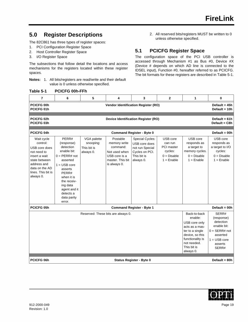
Table 5-1 PCICFG 00h-FFh
7 6 5 4 3 2 1 0
PCICFG 00h Vendor Identification Register (RO) Default = 45hPCICFG 01h Default = 10h
PCICFG 02h Device Identification Register (RO) Default = 61hPCICFG 03h Default = C8h
PCICFG 04h Command Register - Byte 0 Default = 00h
Wait cycle control:
USB core does not need to insert a wait state between address and data on the AD lines. This bit is always 0.
PERR# (response) detection
enable bit:
0 = PERR# not asserted
1 = USB core asserts PERR# when it is the receiv-ing data agent and it detects a data parity error.
VGA palette snooping:
This bit is always 0.
Postable memory write
command:
Not used when USB core is a master. This bit is always 0.
Special Cycles:
USB core does not run Special Cycles on PCI. This bit is always 0.
USB core can run
PCI master cycles:
0 = Disable1 = Enable
USB core responds as a target to
memory cycles.
0 = Disable1 = Enable
USB core responds as
a target to I/O cycles:
0 = Disable1 = Enable
PCICFG 05h Command Register - Byte 1 Default = 00h
Reserved: These bits are always 0. Back-to-back enable:
USB core only acts as a mas-ter to a single device, so this functionality is not needed. This bit is always 0.
SERR# (response) detection enable bit:
0 = SERR# not asserted
1 = USB core asserts SERR#
PCICFG 06h Status Register - Byte 0 Default = 80h
FireLink
Page 20 912-3000-049Revision: 1.0
OPTi®
Fast back-to-back capability:
USB core sup-ports fast back-to-back transac-tions when transactions are not to same agent. This bit is always 1.
Reserved: These bits are always 0.
PCICFG 07h Status Register - Byte 1 Default = 02h
Detected parity error:
This bit is set to 1 whenever the USB core detects a parity error, even if PCICFG 04h[6] is disabled.
Write 1 to clear.
SERR# status:
This bit is set to 1 whenever the USB core detects a PCI address parity error.
Write 1 to clear.
Received master abort
status:
Set to 1 when the USB core, acting as a PCI master, aborts a PCI bus mem-ory cycle.
Write 1 to clear.
Received target abort
status:
This bit is set to 1 when a USB core generated PCI cycle (USB core is the PCI master) is aborted by a PCI target.
Write 1 to clear.
Signaled target abort status:
This bit is set to 1 when the USB core signals tar-get abort.
Write 1 to clear.
DEVSEL timing (RO):
Indicates DEVSEL# timing when performing a positive decode. Since DEVSEL# is asserted to meet the medium timing, these bits are encoded as 01.
Data parity reported:
Set to 1 if PCICFG 04h[6] is set and the USB core detects PERR# asserted while acting as PCI master (whether PERR# was driven by USB core or not.)
PCICFG 08h Revision Identification Register (RO) Default = 10h
PCICFG 09h Class Code Register (RO) Default = 10hPCICFG 0Ah Default = 03hPCICFG 0Bh Default = 0Ch
PCICFG 0Ch Cache Line Size Register Default = 00h
PCICFG 0Dh Master Latency Timer Register Default = 00h
PCICFG 0Eh Header Type Register (RO) Default = 00h
PCICFG 0Fh Reserved Default = 00h
PCICFG 10h-13h Base Address Register 0 Default = 00h
This register identifies the base address of a contiguous memory space in main memory. POST will write all 1s to this register, then read back the value to determine how big of a memory space is requested. After allocating the requested memory, POST will write theupper bytes with the base address.
Bits [31:0] correspond to: 10h = [7:0], 11h = [15:8], 12h = [23:16], 13h = [31:24].- Bit [0] - Indicates that the operational registers are mapped into memory space. Always = 0.- Bits [2:1] - Indicates that the base register is 32 bits wide and can be placed anywhere in 32-bit memory space. Always = 0.- Bit [3] - Indicates no support for prefetchable memory. Always = 0.- Bits [11:4] - Indicates a 4K byte address range is requested, Always = 0.- Bits [31:12] - Base Address: Post writes the value of the memory base address to this register.
PCICFG 14h-2Bh Reserved Default = 00h
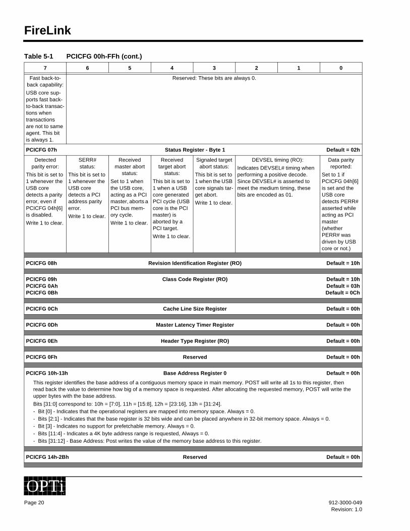
Table 5-1 PCICFG 00h-FFh (cont.)
7 6 5 4 3 2 1 0

FireLink
912-2000-049 Page 21Revision: 1.0
OPTi®
PCICFG 2Ch-2Dh Subsystem Vendor Register (RO) Default = 00h
Subsystem Vendor - Bits [15:0] correspond to: 2Ch = [7:0], 2Dh = [15:8].
- This register can be written to when PCICFG 50h[3] = 0.
PCICFG 2Eh-2Fh Subsystem ID Register (RO) Default = 00h
Subsystem ID - Bits [15:0] correspond to: 2Eh = [7:0], 2Fh = [15:8].
- This register can be written to when PCICFG 50h[3] = 0.
PCICFG 30h-3Bh Reserved Default = 00h
PCICFG 3Ch Interrupt Line Register Default = 00h
This register identifies which of the system interrupt controllers the device’s interrupt pin is connected to. The value of this register is used by device drivers and has no direct meaning to the USB core.
PCICFG 3Dh Interrupt Pin Register Default = 01h
This register identifies which interrupt pin a device uses. Since the USB core uses INTA#, this value is set to 01h.
PCICFG 3Eh Minimum Grant Register (RO) Default = 00h
Reserved
PCICFG 3Fh Maximum Latency Register (RO) Default = 00h
Reserved
PCICFG 40h-43h Reserved Default = 00h
These registers are for internal testing purposes. Do not write to these registers.
PCICFG 44h-4Dh Reserved Default = 00h
PCICFG 4Eh I2C Control Register Default = 00h
Reserved Test 0, Test 1
1 = I/O buffer enabled
0 = disabled
Reads back
I2C data output bit (bit 2)
(RO)
Reads back
I2C clock out-put bit (bit 1)
(RO)
I2C data output:
0 = Output 01 = Output 1
I2C clock output:
0 = Output 01 = Output 1
I2C control:
0 = Disable1 = Enable
PCICFG 4Fh Reserved Default = 00h
PCICFG 50h PCI Host Feature Control Register Default = 00h
CLKRUN# control when enabled (PCICFG 50[2] = 1)0 = Normal1 = Power saving mode(default = 0)
Subsystem Vendor ID Register (PCICFG 2Ch)control:
0= Read-Only
1= Writable
CLKRUN# on host interface):
0 = Disabled, CLKRUN# tristated
1 = Enabled per PCI
Port 2 output:
0 = Enable1 = Disable
(Controls USBI/O cells to save power)
Port 1 output:
0 = Enable1 = Disable
(Controls USBI/O cells to save power)
PCICFG 51h Interrupt Assignment Register Default = 01h
Table 5-1 PCICFG 00h-FFh (cont.)
7 6 5 4 3 2 1 0

FireLink
Page 22 912-3000-049Revision: 1.0
OPTi®
Host controller type:
0 = Viper-N+ (send sin-gle data phase on IRQ drive-back)
1 = FireStar(burst two data phases)
IRQ Driveback:
0 = Disable1 = Enable
Reserved Interrupt Assignment (PCIRQ0# Default) - Interrupts from the USB are mapped to this interrupt. Note that if an IRQ (an edge-mode interrupt) is selected, this IRQ must be pro-grammed to Level mode on the host chipset.
Level Mode:00000 = Disabled 00110 = ACPI101011 = ACPI600001 = PCIRQ0# (Default) 00111 = ACPI201100 = ACPI700010 = PCIRQ1# 01000 = ACPI301101 = ACPI800011 = PCIRQ2# 01001 = ACPI401110 = ACPI900100 = PCIRQ3# 01010 = ACPI501111 = ACPI1000101 = ACPI0
Edge Mode:10000 = IRQ0 10110 = IRQ611011 = IRQ1110001 = IRQ1 10111 = IRQ711100 = IRQ1210010 = IRQ2 11000 = IRQ811101 = IRQ1310011 = IRQ3 11001 = IRQ911110 = IRQ1410100 = IRQ4 11010 = IRQ1011111 = IRQ1510101 = IRQ5
PCICFG 52h Strap Option Override
Reserved PCI Voltage0 = 3.3V1 = 5V (default = 1)
Reserved Test Mode0 = Opera-tional1 = TXD test mode(default = 0)
PWRFLT2polarity1 = Low0 = High (default = 1)
PWRFLT1polarity1 = Low0 = High(default = 1)
PWRON1 &PWRON2polarity1 = Low0 = High(default = 0)
PCICFG 53h Reserved Default = 00h
PCICFG 54h-57h IRQ Driveback Address Register - Byte 0: Address Bits [7:0] Default = 33333330h
IRQ Driveback Protocol Address Bits: Bits [31:0] correspond to: 54h = [7:0], 55h = [15:8], 56h = [23:16], 57h = [31:24].
- When the FireLink/FireBlast logic must generate an interrupt from any source, it follows the IRQ Driveback Protocol and toggles the REQ# line to the host. Once it has the bus, it writes the changed IRQ information to the 32-bit I/O address specified in this register. The host interrupt controller claims this cycle and latches the new IRQ values.
- Bits 1:0 are reserved to be 00 and are read-only.
PCICFG 58h-6Bh Reserved Default = 00h
PCICFG 6Ch-6Fh Test Mode Enable Register Default = 00h
Reserved
Table 5-1 PCICFG 00h-FFh (cont.)
7 6 5 4 3 2 1 0

FireLink
912-2000-049 Page 23Revision: 1.0
OPTi®
5.2 Host Controller Register SpaceThis register space is the operational control block in the USBcore. It is responsible for the host controller operationalstates (Suspend, Disabled, Enabled), special USB signaling(Reset, Resume), status, interrupt control, and host controllerconfiguration information.
The host controller (HC) interface registers are PCI memorymapped I/O, hereafter referred to as MEMOFST. The bit for-mats for these registers are described in Table 5-2.
Table 5-2 MEMOFST 00h-5Ch
7 6 5 4 3 2 1 0
MEMOFST 00h HcRevision Register (RO) Default = 10hMEMOFST 01h-03h Default = 000001h
Bits [31:0] correspond to: 00h = [7:0], 01h = [15:8], 02h = [23:16], 03h = [31:24]
- Bits [7:0] Revision - Indicates the Open HCI Specification revision number implemented by hardware (X.Y = XYh). FireLink support Specification 1.0.
- Bits [31:8] Reserved
MEMOFST 04h HcControl Register - Byte 0 Default = 00h
HC Functional State:
00 = USB Reset01 = USB Resume10 = USB Operational11 = USB Suspend
The HC may force a state change from USB Suspend to USB Resume after detecting resume signaling from a downstream port.
Processing of Bulk List:
0 = Disable1 = Enable
Processing of Control List:
0 = Disable1 = Enable
Disable Isoch-ronous List
when Periodic List is
enabled:(1)
0 = Yes1 = No
Processing of Periodic (inter-rupt and isoch-
ronous) List:
0 = Disable1 = Enable
The HC checks this bit prior to attempting any periodic trans-fers in a frame.
Control Bulk Service Ratio:
Specifies the number of control endpoints serviced for every bulk endpoint. Encoding is N–1 where N is the number of control end-points (i.e., 00 = 1 control end-point; 11 = 4 control endpoints).
(1) Disabling the Isochronous List when the Periodic List is enabled allows interrupt endpoint descriptors to be serviced. While processing the Period List, the HC will check bit 3 when it finds an isochronous endpoint descriptor.
MEMOFST 05h HcControl Register - Byte 1 Default = 00h
Reserved Remote Wakeup Con-
nected Enable:
If a remote wakeup signal is supported, this bit is used to enable that operation. Since there is no remote wakeup signal supported, this bit is ignored.
Remote Wakeup Con-nected (RO):
Indicates whether the HC supports a remote wakeup signal. This implementation does not sup-port any such signal. The bit is hardcoded to 0.
Interrupt Routing:
0 = Interrupts routed to normal interrupt mechanism (INTA#)
1 = Interrupts routed to SMI
Also see PCICFG 51h
MEMOFST 06h-07h HcControl Register - Bytes 2 & 3 Default = 00h
Reserved
MEMOFST 08h HcCommandStatus Register - Byte 0 Default = 00h

FireLink
Page 24 912-3000-049Revision: 1.0
OPTi®
Reserved Ownership Change Request:
When set by software, this bit sets the Owner-ship Change bit (MEMOFST 0Fh[6]).
Cleared by soft-ware.
Bulk List has an active endpoint
descriptor?(1)
0 = No1 = Yes
Control List has an active endpoint
descriptor?(1)
0 = No1 = Yes
HC Reset:
Writing a 1 ini-tiates a soft-ware reset.
This bit is cleared by the HC upon com-pletion of reset operation.
(1) The bit may be set by either software or the HC. It is cleared by the HC each time it begins processing the head of the list (Bulk List for bit 2, Control List for bit 1)
MEMOFST 09h HcCommandStatus Register - Byte 1 Default = 00h
Reserved
MEMOFST 0Ah HcCommandStatus Register - Byte 2 Default = 00h
Reserved Schedule Overrun Count:
This field increments every time the Scheduling Overrun bit (MEMOFST 0Ch[0] is set. The count wraps from 11 to 00.
MEMOFST 0Bh HcCommandStatus Register - Byte 3 Default = 00h
Reserved
MEMOFST 0Ch HcInterrupt Status Register - Byte 0* Default = 00h
Reserved Root Hub Status Change:
This bit is set when the con-tent of HcRh Status (50h-53h) or the con-tent of any HcRhPort Sta-tus Register (54h-5Bh) has changed.
Frame Number Overflow:
This bit is set when MEMOFST 3Ch[15] (Frame Num-ber Register) changes from 0-to-1 or from 1-to-0.
Unrecoverable Error:
This event is not imple-mented and is hardcoded to 0. All writes are ignored.
Resume Detected:
This bit is set when the HC detects resume signaling on a downstream port.
Start of Frame:
This bit is set when the Frame Management block signals a "Start of Frame" event.
Writeback Done Head:
This bit is set after the Host Controller has written HcDone-Head to Hcca-DoneHead.
Scheduling Overrun
occurred?
0 = No1 = Yes
MEMOFST 0Dh-0Eh HcInterruptStatus Register - Bytes 1 & 2 Default = 00h
Reserved
MEMOFST 0Fh HcInterruptStatus Register - Byte 3* Default = 00h
Reserved Ownership Change:
This bit is set when the Own-ership Change Request bit (MEMOFST 08h[3]) is set.
Reserved
* Writing a 1 to a bit in this register clears the corresponding bit, while writing a 0 leaves the bit unchanged.
Table 5-2 MEMOFST 00h-5Ch
7 6 5 4 3 2 1 0

FireLink
912-2000-049 Page 25Revision: 1.0
OPTi®
MEMOFST 10h HcInterruptEnable Register - Byte 0* Default = 00h
Reserved Allow interrupt generation due
to Root Hub Status Change:
0 = Ignore1 = Enable
Allow interrupt generation due to Frame Num-ber Overflow:
0 = Ignore1 = Enable
Reserved
All writes to this bit are ignored.
Allow interrupt generation due
to Resume Detected:
0 = Ignore1 = Enable
Allow interrupt generation due
to Start of Frame:
0 = Ignore1 = Enable
Allow interrupt generation due
to Writeback Done Head:
0 = Ignore1 = Enable
Allow interrupt generation due to Scheduling
Overrun:
0 = Ignore1 = Enable
MEMOFST 11h-12h HcInterruptEnable Register - Bytes 1 & 2 Default = 00h
Reserved
MEMOFST 13h HcInterruptEnable Register - Byte 3* Default = 00h
Master inter-rupt generation:
0 = Ignore
1 = Allows all interrupts to be enabled in 10h-13h.
Allow interrupt generation due to Ownership
Change:
0 = Ignore1 = Enable
Reserved
* Writing a 1 to a bit in this register sets the corresponding bit, while writing a 0 leaves the bit unchanged.
MEMOFST 14h HcInterruptDisable Register - Byte 0* Default = 00h
Reserved Allow interrupt generation due
to Root Hub Status Change:
0 = Ignore1 = Disable
Allow interrupt generation due to Frame Num-ber Overflow:
0 = Ignore1 = Disable
Reserved
All writes to this bit are ignored.
Allow interrupt generation due
to Resume Detected:
0 = Ignore1 = Disable
Allow interrupt generation due
to Start of Frame:
0 = Ignore1 = Disable
Allow interrupt generation due
to Writeback Done Head:
0 = Ignore1 = Disable
Allow interrupt generation due to Scheduling
Overrun:
0 = Ignore1 = Disable
MEMOFST 15h-16h HcInterruptDisable Register - Bytes 1 & 2 Default = 00h
Reserved
MEMOFST 17h HcInterruptDisable Register - Byte 3* Default = 00h
Master inter-rupt generation:
0 = Ignore
1 = Allows all interrupts to be dis-abled in 10h-13h.
Allow interrupt generation due to Ownership
Change:
0 = Ignore1 = Disable
Reserved
* Writing a 1 to a bit in this register clears the corresponding bit, while writing a 0 leaves the bit unchanged.
MEMOFST 18h-1Bh HcHCCA Register Default = 00h
Bits [31:0] correspond to: 18h = [7:0], 19h = [15:8], 1Ah = [23:16], 1Bh = [31:24].
- Bits [7:0] Reserved
- Bits [31:8] Pointer to HCCA base address
MEMOFST 1Ch-1Fh HcPeriodCurrentED Register Default = 00h
Bits [31:0] correspond to: 1Ch = [7:0], 1Dh = [15:8], 1Eh = [23:16], 1Fh = [31:24].
- Bits [3:0] Reserved
- Bits [31:4] Pointer to current Periodic List End Descriptor
Table 5-2 MEMOFST 00h-5Ch
7 6 5 4 3 2 1 0

FireLink
Page 26 912-3000-049Revision: 1.0
OPTi®
MEMOFST 20h-23h HcControlHeadED Register Default = 00h
Bits [31:0] correspond to: 20h = [7:0], 21h = [15:8], 22h = [23:16], 23h = [31:24].
- Bits [3:0] Reserved
- Bits [31:4] Pointer to current Control List Head End Descriptor
MEMOFST 24h-27h HcControlCurrent ED Default = 00h
Bits [31:0] correspond to: 24h = [7:0], 25h = [15:8], 26h = [23:16], 27h = [31:24].
- Bits [3:0] Reserved
- Bits [31:4] Pointer to current End Descriptor in Control Listfdfdsdf
MEMOFST 28h-2Bh HcBulkHeadED Register Default = 00h
Bits [31:0] correspond to: 28h = [7:0], 29h = [15:8], 2Ah = [23:16], 2Bh = [31:24].
- Bits [3:0] Reserved
- Bits [31:4] Pointer to current Bulk List Head End Descriptor in Control List
MEMOFST 2Ch-2Fh HcBulkCurrentED Register Default = 00h
Bits [31:0] correspond to: 2Ch = [7:0], 2Dh = [15:8], 2Eh = [23:16], 2Fh = [31:24].
- Bits [3:0] Reserved
- Bits [31:4] Pointer to current Bulk List End Descriptor
MEMOFST 30h-33h HcDoneHead Register Default = 00h
Bits [31:0] correspond to: 30h = [7:0], 31h = [15:8], 32h = [23:16], 33h = [31:24].
- Bits [3:0] Reserved
- Bits [31:4] Pointer to current Done List Head End Descriptor
MEMOFST 34h-37h HcFmInterval Register Default =
Bits [31:0] correspond to: 34h = [7:0], 35h = [15:8], 36h = [23:16], 37h = [31:24].
- Bits [13:0] Frame Interval - These bits specify the length of a frame as (bit times – 1). For 12,000 bit times in a frame, a value of 11,999 is stored here. (Default = 2EDFh)
- Bits [15:14] Reserved
- Bits [30:16] FS Largest Data Packet: These bits specify a value which is loaded into the Largest Data Packet Counter at the beginning of each frame.
- Bit 31 Frame Interval Toggle - This bit is toggled by HCD whenever it loads a new value into the Frame Interval bits (bits [13:0]).
MEMOFST 38h-3Bh HcFrameRemaining Register Default = 00h
Bits [31:0] correspond to: 38h = [7:0], 39h = [15:8], 3Ah = [23:16], 3Bh = [31:24].
- Bits [13:0] Frame Remaining (RO) - This 14-bit decrementing counter is used to time a frame. When the HC is in the USB Operational state, the counter decrements each 12MHz clock period. When the count reaches 0, the end of a frame has been reached. The counter reloads with Frame Interval (MEMOFST 34h[13:0]) at that time. In addition, the counter loads when the HC transitions into the USB Operational state.
- Bits [30:14] Reserved
- Bit 31 Frame Remaining Toggle (RO) - This bit is loaded with Frame Interval Toggle (MEMOFST 34h[31]) when Frame Remaining (bits [13:0]) is loaded.
Table 5-2 MEMOFST 00h-5Ch
7 6 5 4 3 2 1 0

FireLink
912-2000-049 Page 27Revision: 1.0
OPTi®
MEMOFST 3Ch-3Fh HcFmNumber Register Default = 00h
Bits [31:0] correspond to: 3Ch = [7:0], 3Dh = [15:8], 3Eh = [23:16], 3Fh = [31:24].
- Bits [15:0] Frame Number (RO) - This 16-bit incrementing counter is incremented coincident with the load of Frame Remaining (MEMOFST 38h[13:0]). The count will roll over from FFFh to 0h.
- Bits [31:16] Reserved
MEMOFST 40h-43h HcPeriodicStart Register Default = 00h
Bits [31:0] correspond to: 40h = [7:0], 41h = [15:8], 42h = [23:16], 43h = [31:24].
- Bits [13:0] Periodic Start - These bits are used by the List Processor to determine where in a frame the Periodic List processing must begin.
- Bits [31:14] Reserved
MEMOFST 44h-47h HcLSThreshold Register Default = 00h
Bits [31:0] correspond to: 44h = [7:0], 45h = [15:8], 46h = [23:16], 47h = [31:24].
- Bits [11:0] LS Threshold - These bits contain a value used by the Frame Management Block to determine whether or not a low speed transaction can be started in the current frame.
- Bits [31:12] Reserved
MEMOFST 48h HcRhDescriptorA Register - Byte 0 (RO) Default = 02h
Number Downstream Ports - The USB core supports two downstream ports.
MEMOFST 49h HcRhDescriptorA Register - Byte 1 Default = 00h
Reserved No Over-current Protection:(1)
0 = Over-cur-rent status is reported
1 = Over-cur-rent status is not reported
Over-current Protection
Mode:
0 = Global over-current
1 = Individual Over-Cur-rent
This bit is only valid when bit 4 is cleared.
This bit should be written to 0.
Device Type (RO):
The USB core is not a com-pound device.
No Power Switching:(1)
0 = Ports are powered switched
1 = Ports are always pow-ered on
Power Switch-ing Mode:
0 = Global switching
1 = Individual switching
This bit is only valid when bit 1 is cleared.
This bit should be written to 0.
(1) Bits 4 and 1 should be written to support the external system port over-current and switching implementations.
MEMOFST 4Ah HcRhDescriptorA Register - Byte 2 Default = 00h
Reserved
MEMOFST 4Bh HcRhDescriptorA Register - Byte 3 Default = 01h
Power-On to Power-Good Time
- The USB core power switching is effective within 2ms. The field value is represented as the number of 2ms intervals. This field should be written to support the system implementation. This field should always be written to a non-zero value.
Table 5-2 MEMOFST 00h-5Ch
7 6 5 4 3 2 1 0

FireLink
Page 28 912-3000-049Revision: 1.0
OPTi®
MEMOFST 4Ch-4Dh HcRhDescriptorB Register - Bytes 0 & 1 Default = 00h
Bits [15:0] correspond to: 4Ch = [7:0], 4Dh = [15:8].
- Bit 0 Reserved
- Bits [15:1] Device Removable - USB core ports default to removable devices:0 = Device not removable1 = Device removable
Bit 15 corresponds to Port 15, Bit 14 corresponds to Port 14, the remaining bits follow suit. Unimplemented ports are reserved.
MEMOFST 4Eh-4Fh HcRhDescriptorB Register- Bytes 2 & 3 Default = 00h
Bits [15:0] correspond to: 4Eh = [7:0], 4Fh = [15:8].
- Bit 0 Reserved
- Bits [15:1] Port Power Control Mask: Bit 15 corresponds to Port 15, Bit 14 corresponds to Port 14, the remaining bits follow suit.Unimplemented ports are reserved.0 = Device not removable1 = Global power mask
This field is only valid if No Power Switching bit (MEMOFST 49h[1]) is cleared and Power Switching Mode Bit (MEMOFST 49h[0]) is set (individual port switching). When set, the port only responds to individual port power switching commands (Set/ClearPortPower, MEMOFST 54h[1:0] and 58h[1:0]). When cleared, the port only responds to global power switching commands (Set/ClearGlobalPower, MEMOFST 52h[0] and 50h[0]).
MEMOFST 50h HcRhStatus Register - Byte 0 Default = 00h
Reserved Over-current Indicator (RO):(1)
Reflects state of OVCR pin.
0 = No over-cur-rent condi-tion
1 = Over-cur-rent condi-tion
Read: Local Power Status
Not supported. Always read 0.
Write: Clear Global Power
0 = No effect
1 = Issue Clear Global Power com-mand to ports
(1) Bit 1 is only valid if the No Over-current Protection (MEMOFST 49h[4]) and Over-current Protection Mode (MEMOFST 49h[3]) bits are cleared.
MEMOFST 51h HcRhStatus Register - Byte 1 Default = 00h
Read: Device Remote Wake-up Enable(1)
0 = Disabled1 = Enabled
Write: Set Remote Wake-up Enable
0 = No effect
1 = Sets Device Remote Wakeup Enable
Reserved
(1) Allows ports’ Connect Status Change Bit (MEMOFST 56h[0] for Port 1 and MEMOFST 59h[0] for Port 2) as a remote wakeup event.
Table 5-2 MEMOFST 00h-5Ch
7 6 5 4 3 2 1 0

FireLink
912-2000-049 Page 29Revision: 1.0
OPTi®
MEMOFST 52h HcRhStatus Register - Byte 2 Default = 00h
Reserved Over-current Indicator Change
This bit is set when the Over-current Indica-tor bit (MEMOFST 50h[1]) changes.
Write 1 to clear
Read: Local Power Status Change
Not supported. Always read 0
Write: Set Glo-bal Power
0 = No effect
1 = Issue Set Global Power com-mand to ports
MEMOFST 53h HcRhStatus Register - Byte 3 Default = 00h
Clear Remote Wakeup
Enable (WO)
0 = No effect
1 = Clear Device Remote Wakeup Enable bit (MEMOFST 51h[7])
Reserved
MEMOFST 54h HcRhPort1Status Register - Byte 0 Default = 00h
Reserved Read: Port Reset Status
0 = Port reset status sig-nal not active
1 = Port reset signal active
Write: Set Port Reset
0 = No effect
1 = Sets Port Reset Sta-tus
Read: Port Over-current Indicator(1)
0 = No over-cur-rent condi-tion
1 = Over-cur-rent condi-tion
Write: Clear Port Suspend
0 = No effect
1 = Initiates selective resume sequence for the port
Read: Port Sus-pend Status
0 = Port is not suspended
1 = Port is selectively suspended
Write: Set Port Suspend
0 = No effect
1 = Sets Port Suspend Status
Read: Port Enable Status
0 = Port dis-abled
1 = Port enabled
Write: Set Port Enable
0 = No effect
1 = Sets Port Enable Sta-tus
Read: Current Connect Status
0 = No device connected
1 = Device con-nected.(2)
Write: Clear Port Enable
0 = No effect
1 = Clears Port Enable Sta-tus bit (bit 1)
(1) The USB core supports global over-current reporting. This bit reflects the state of the OVRCUR pin dedicated to this port. This bit is only valid if the No Over-current Protection (MEMOFST 49h[4]) bit is cleared and Over-current Protection Mode (MEMOFST 49h[3]) bit is set.
(2) If the Device Removable bits (MEMOFST 4Ch[15:0]) are set (not removable), bit 0 is always 1.
Table 5-2 MEMOFST 00h-5Ch
7 6 5 4 3 2 1 0

FireLink
Page 30 912-3000-049Revision: 1.0
OPTi®
MEMOFST 55h HcRhPort1Status Register - Byte 1 Default = 00h
Reserved Read: Low Speed Device Attached(1)
0 = Full speed device
1 = Low speed device
Write: Clear Port Power
0 = No effect
1 = Clears Port Power Sta-tus (bit 0)
Read: Port Power Status(2)
0 = Port power is off
1 = Port power is on
Write: Set Port Power
0 = No effect
1 = Sets Port Power Sta-tus
(1) Bit 1 defines the speed (and bus idle) of the attached device. It is only valid when Current Connect Status (MEMOFST 54h[0]) bit is set.
(2) Bit 0 reflects the power state of the port regardless of the power switching mode. If the No Power Switching (MEMOFST 49h[1]) bit is set, bit 0 is always read as 1.
MEMOFST 56h HcRhPort1Status Register - Byte 2 Default = 00h
Reserved Port Reset Status Change
0 = Port reset is not com-plete
1 = Port reset is complete
Port Over-current Indica-
tor Change
This bit is set when the Over-current Indica-tor (MEMOFST 50h[1]) bit changes.
Write 1 to clear
Port Suspend Status Change
Indicates the completion of the selective resume sequence for the port.
0 = Port is not resumed
1 = Port resume is complete
Port Enable Status Change
Indicates that the port has been disabled due to a hard-ware event (cleared Port Enable Status, MEMOFST 54h[1]).
0 = Port has not been dis-abled
1 = Port Enable Status has been cleared
Connect Status Change
Indicates a con-nect or discon-nect event has been detected.
0 = No con-nect/discon-nect event
1 = Hardware detection of connect/dis-connect event(1)
Write 1 to clear
(1) If the Device Removable Bits (MEMOFST 4Ch[15:1]) are set, bit 0 resets to 1.
MEMOFST 57h HcRhPort1Status Register - Byte 3 Default = 00h
Reserved
Table 5-2 MEMOFST 00h-5Ch
7 6 5 4 3 2 1 0
FireLink
912-2000-049 Page 31Revision: 1.0
OPTi®
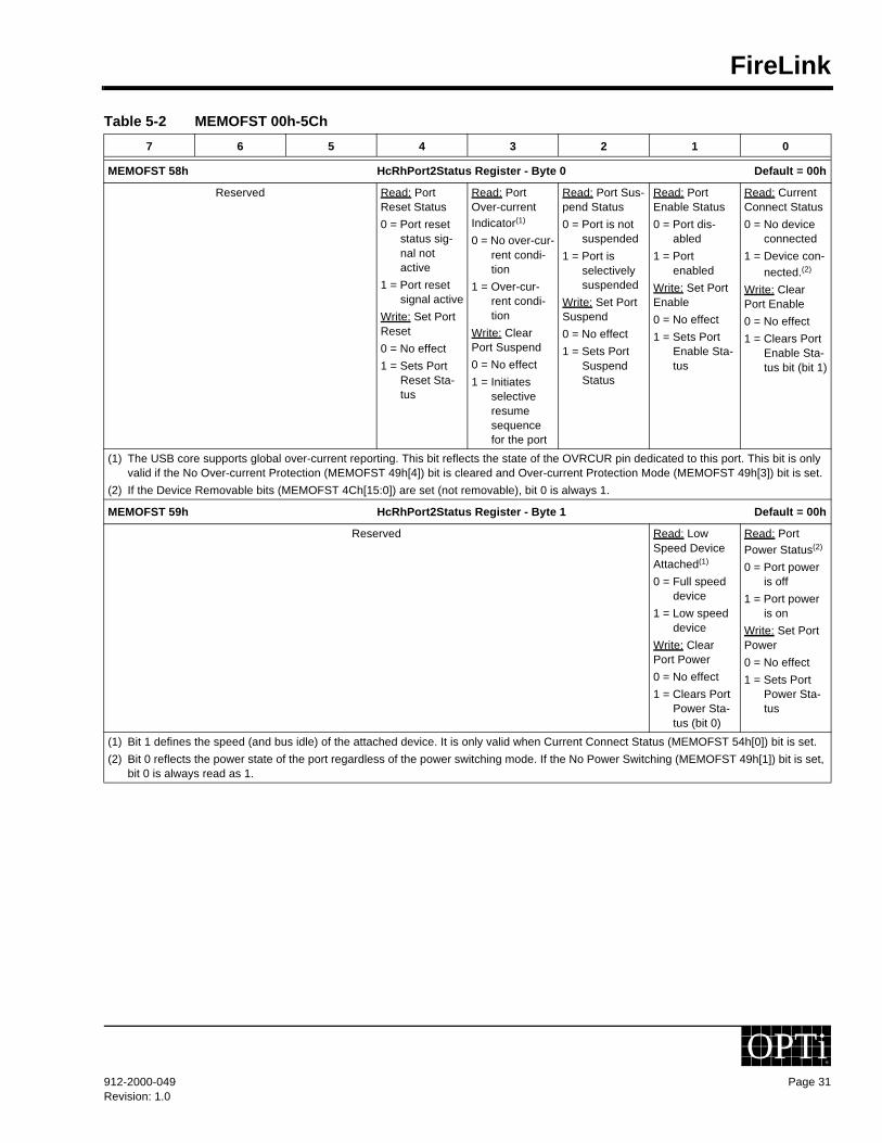
MEMOFST 58h HcRhPort2Status Register - Byte 0 Default = 00h
Reserved Read: Port Reset Status
0 = Port reset status sig-nal not active
1 = Port reset signal active
Write: Set Port Reset
0 = No effect
1 = Sets Port Reset Sta-tus
Read: Port Over-current Indicator(1)
0 = No over-cur-rent condi-tion
1 = Over-cur-rent condi-tion
Write: Clear Port Suspend
0 = No effect
1 = Initiates selective resume sequence for the port
Read: Port Sus-pend Status
0 = Port is not suspended
1 = Port is selectively suspended
Write: Set Port Suspend
0 = No effect
1 = Sets Port Suspend Status
Read: Port Enable Status
0 = Port dis-abled
1 = Port enabled
Write: Set Port Enable
0 = No effect
1 = Sets Port Enable Sta-tus
Read: Current Connect Status
0 = No device connected
1 = Device con-nected.(2)
Write: Clear Port Enable
0 = No effect
1 = Clears Port Enable Sta-tus bit (bit 1)
(1) The USB core supports global over-current reporting. This bit reflects the state of the OVRCUR pin dedicated to this port. This bit is only valid if the No Over-current Protection (MEMOFST 49h[4]) bit is cleared and Over-current Protection Mode (MEMOFST 49h[3]) bit is set.
(2) If the Device Removable bits (MEMOFST 4Ch[15:0]) are set (not removable), bit 0 is always 1.
MEMOFST 59h HcRhPort2Status Register - Byte 1 Default = 00h
Reserved Read: Low Speed Device Attached(1)
0 = Full speed device
1 = Low speed device
Write: Clear Port Power
0 = No effect
1 = Clears Port Power Sta-tus (bit 0)
Read: Port Power Status(2)
0 = Port power is off
1 = Port power is on
Write: Set Port Power
0 = No effect
1 = Sets Port Power Sta-tus
(1) Bit 1 defines the speed (and bus idle) of the attached device. It is only valid when Current Connect Status (MEMOFST 54h[0]) bit is set.
(2) Bit 0 reflects the power state of the port regardless of the power switching mode. If the No Power Switching (MEMOFST 49h[1]) bit is set, bit 0 is always read as 1.
Table 5-2 MEMOFST 00h-5Ch
7 6 5 4 3 2 1 0

FireLink
Page 32 912-3000-049Revision: 1.0
OPTi®
MEMOFST 5Ah HcRhPort2Status Register - Byte 2 Default = 00h
Reserved Port Reset Status Change
0 = Port reset is not com-plete
1 = Port reset is complete
Port Over-current Indica-
tor Change
This bit is set when the Over-current Indica-tor (MEMOFST 50h[1]) bit changes.
Write 1 to clear
Port Suspend Status Change
Indicates the completion of the selective resume sequence for the port.
0 = Port is not resumed
1 = Port resume is complete
Port Enable Status Change
Indicates that the port has been disabled due to a hard-ware event (cleared Port Enable Status, MEMOFST 54h[1]).
0 = Port has not been dis-abled
1 = Port Enable Status has been cleared
Connect Status Change
Indicates a con-nect or discon-nect event has been detected.
0 = No con-nect/discon-nect event
1 = Hardware detection of connect/dis-connect event(1)
Write 1 to clear
(1) If the Device Removable Bits (MEMOFST 4Ch[15:1]) are set, bit 0 resets to 1.
MEMOFST 5Bh HcRhPort2 Status Register - Byte 3 Default = 00h
Reserved
Table 5-2 MEMOFST 00h-5Ch
7 6 5 4 3 2 1 0

FireLink
912-2000-049 Page 33Revision: 1.0
OPTi®
5.2.1 Legacy Support RegistersFour registers are provided for legacy support:
• HceControl - Used to enable and control the emulation hardware and report various status information.
• HceInput- Emulation side of the legacy Input Buffer register.
• HceOutput- Emulation side of the legacy Output Buffer register where keyboard and mouse data is to be written by software.
• HceStatus- Emulation side of the legacy Status register.
These registers are located in the Host Controller Register Space; from MEMOFST 100h through 10Fh. The bit formats forthese registers are described in Table 5-3.
Refer to Section 4.1.3, "Legacy Support" for information when accessing these registers when emulation is enabled.
Table 5-3 MEMOFST 100h-1Fh (Legacy Support Registers)
7 6 5 4 3 2 1 0
MEMOFST 100h HceControl Register - Byte 0 Default = 00h
IRQ12 Active
Indicates that a positive transi-tion of IRQ12 from kybrd con-troller has occurred.
Writing a 1 clears this bit, while writing a 0 leaves it unchanged.
IRQ1 Active
Indicates that a positive transi-tion of IRQ1 from kybrd con-troller has occurred.
Writing a 1 clears this bit, while writing a 0 leaves it unchanged.
GateA20 Sequence
Set by HC when a data value of D1h is written to Port 64h.
Cleared by HC on write to Port 64h of any value other than D1h.
External IRQEn
IRQ1 and IRQ12 from kybrd controller causes emula-tion interrupt:
0 = Disable1 = Enable
This bit is inde-pendent of the Emulation Enable bit (bit 0) setting.
IRQEn
If the Output Full bit (MEMOFST 10Ch[0]) = 1, HC generates IRQ1 or IRQ12.
If the Aux Out-put Full bit (MEMOFST 10Ch[5]) = 0, HC generates IRQ1; if = 1, HC generates IRQ12.
0 = Disable1 = Enable
Character Pending
HC generates emulation inter-rupt when the Output Full bit (MEMOFST 10Ch[0]) = 0.
0 = Disable1 = Enable
Emulation Interrupt (RO)
A static decode of the emula-tion interrupt condition.
Emulation Enable
HC is enabled for legacy emu-lation?
0 = No1 = Yes(1)
(1) The HC decodes accesses to Ports 60h/64h and generates IRQ1 and/or IRQ12 when appropriate. Additionally, the HC generates an emu-lation interrupt at appropriate times to invoke the emulation software.
MEMOFST 101h HceControl Register - Byte 1 Default = 00h
Reserved A20 State:
Indicates cur-rent state of Gate A20 on kybrd control-ler. Used to compare against value written to Port 60h when GateA20 Sequence is active.
MEMOFST 102h-103h HceControl Register - Bytes 2 & 3 Default = 00h
Reserved

FireLink
Page 34 912-3000-049Revision: 1.0
OPTi®
MEMOFST 104h HceInput Register - Bytes 0 Default = 00h
Input Data:
- I/O data that is written to Ports 60h and 64h is captured in this register.
Note: Refer to Table 4-4, “Emulated Registers and Side Effects,” on page 18 if emulation is enabled.
MEMOFST 105h-107h HceInput Register - Bytes 1-3 Default = 00h
Reserved
MEMOFST 108h HceOutput Register - Bytes 0 Default = 00h
Output Data:
- This register hosts data that is returned when an I/O read of Port 60h is performed by application software.
Note: Refer to Table 4-4, “Emulated Registers and Side Effects,” on page 18 if emulation is enabled.)
MEMOFST 109h-10Bh HceOutput Register - Bytes 1-3 Default = 00h
Reserved
MEMOFST 10Ch HceStatus Register - Byte 0 Default = 00h
Parity
Indicates parity error on key-board/mouse data.
Time-out
Used to indicate a time-out
Aux Output Full
Assert IRQ12 if Output Full bit (MEMOFST 10Ch[0]) = 1 and IRQEn bit (MEMOFST 100h[3]) = 1?
0 = No1 = Yes
Inhibit Switch
Reflects state of the keyboard inhibit switch:
0 = Inhibited1 = Not inhibited
Cmd Data
HC sets this bit on I/O writes to Ports 60h and 64h:
0 = Port 60h1 = Port 64h
Flag
Nominally used as a system flag by software to indicate a warm or cold boot.
Input Full
HC sets this bit to 1 on an I/O write to Port 60h or 64h except for the case of a GateA20 Sequence. While set to 1 and emulation is enabled (MEMOFST 100h[0] = 1), an emulation interrupt condi-tion exists.
Output Full
HC sets this bit to 0 on a read of Port 60h. While this bit is 0 and the Character Pending bit (MEMOFST 100h[2]) = 1, an emulation interrupt condi-tion exists.
Setting this bit to 1 will gener-ate either IRQ1 or IRQ12 under certain condi-tions(1).
(1) If the IRQEn bit (MEMOFST 100h[3]) = 1 and Aux Output Full bit (MEMOFST 10Ch[5]) = 0: IRQ1 is generated.If the IRQEn bit (MEMOFST 100h[3]) = 1 and Aux Output Full bit (MEMOFST 10Ch[5]) = 1: IRQ12 is generated.
Note: Refer to Table 4-4, “Emulated Registers and Side Effects,” on page 18 if emulation is enabled.
MEMOFST 10Dh-10Fh HceStatus Register - Bytes 1-3 Default = 00h
Reserved
Table 5-3 MEMOFST 100h-1Fh (Legacy Support Registers)
7 6 5 4 3 2 1 0

FireLink
912-2000-049 Page 35Revision: 1.0
OPTi®
6.0 Electrical RatingsStresses above those listed in the following tables may cause permanent damage to the device. These are stress ratings onlyand functional operation of the device at these or any other conditions above those indicated in the operational sections of thisspecification are not implied.
6.1 Absolute Maximum Ratings
6.2 DC Characteristics: VCC = 3.3V or 5.0V ±5%, TA = 0°C to +70°C
Symbol Parameter
5.0 Volt 3.3 Volt
UnitMin Max Min Max
VCC Supply Voltage +6.5 +4.0 V
VI Input Voltage –0.5 VCC + 0.5 –0.5 VCC + 0.5 V
VO Output Voltage –0.5 VCC + 0.5 –0.5 VCC + 0.5 V
TOP Operating Temperature 0 +70 0 +70 °C
TSTG Storage Temperature –40 +125 –40 +125 °C
Symbol Parameter Min Max Unit Condition
VIL Input low Voltage –0.5 +0.8 V
VIH Input high Voltage +2.0 VCC + 0.5 V
VOL Output low Voltage +0.4 V IOL = 4.0mA
VOH Output high Voltage +2.4 V IOH = -1.6mA
IIL Input Leakage Current +10.0 µA VIN = VCC
IOZ Tristate Leakage Current +10.0 µA
CIN Input Capacitance +10.0 pF
COUT Output Capacitance +10.0 pF
ICC Power Supply Current: 3.3V Core 45mA typical during Normal opera-tion,
below 1mA at Standby

FireLink
Page 36 912-3000-049Revision: 1.0
OPTi®
6.3 AC Characteristics (Preliminary)
6.3.1 PCI Bus AC Timings
Figure 6-1 Setup Timing Waveform
Figure 6-2 Hold Timing Waveform
Sym Parameter Min Max Unit Figure
t100 C/BE[3:0]#, AD[31:0], FRAME#, IRDY#, TRDY#, STOP#, DEVSEL#, LOCK#, PAR, SERR#, PERR# setup time to PCICLK rising
7 ns 6-1
t101 C/BE[3:0]#, AD[31:0], FRAME#, IRDY#, TRDY#, STOP#, DEVSEL#, LOCK#, PAR, SERR#, PERR# hold time from PCICLK rising
0 ns 6-2
t102 C/BE[3:0]#, AD[31:0], FRAME#, IRDY#, TRDY#, STOP#, DEVSEL#, LOCK#, PAR, SERR#, PERR# valid delay from PCICLK rising
2 11 ns 6-3
t103 REQ# setup time to PCICLK rising 12 ns 6-1
t104 REQ# hold time from PCICLK rising 0 ns 6-2
t105 GNT# valid delay from PCICLK rising 2 12 ns 6-3
0ns 50ns 100ns
t100, t103
PCICLK
SIGNAL
t101, t104
0ns 50ns 100ns
PCICLK
SIGNAL

FireLink
912-2000-049 Page 37Revision: 1.0
OPTi®
Figure 6-3 Output Delay Timing Waveform
6.3.2 USB AC Timings: Full Speed Source
Sym Parameter Min Max Unit Figure Condition (Notes 1, 2, and 3)
Driver Characteristics
tRtF
Transition Time:Rise TimeFall Time
44
2020
nsns
CL = 50pF, Notes 5 and 6
tRFM Rise/Fall Time Matching 90 110 % (tR/tF)
vCRS Output Signal Crossover Voltage 1.3 2.0 V
zDRV Driver Output Resistance 28 43 ohm Steady state drive
Data Source Timings
tDRATE Full Speed Data Rate 11.97 12.03 Mb/s Average bit rate = 12Mb/s ±0.25%
tFRAME Frame Interval 0.9995 1.0005 ms 1.0ms ±0.05%
tDJ1tDJ2
Source Differential Driver Jitter:To Next TransitionFor Paired Transitions
–3.5–4.0
3.54.0
nsns
Notes 7 and 8
tEOPT Source EOP Width 160 175 ns Note 8
tDEOP Differential to EOP Transition Skew –2 5 ns Note 8
tJR1tJR2
Receiver Data Jitter Tolerance:To Next TransitionFor Paired Transitions
–18.5–9
18.59
nsns
Note 8
tEOPR1tEOPR2
EOP Width at Receiver:Must Reject at EOPMust Accept as EOP
4082
nsns
Note 8
0ns 50ns 100ns
PCICLK
SIGNAL
t102, t105

FireLink
Page 38 912-3000-049Revision: 1.0
OPTi®
6.3.3 USB AC Timings: Low Speed Source
Notes: 1. All voltages measured from the local ground potential, unless otherwise specified.
2. All timings use a capacitive load (CL) to ground of 50pF, unless otherwise specified.
3. Full speed timings have a 1.5 kohm pull-up to 2.8V on the D+ data line.
4. Low speed timings have a 1.5 kohm pull-up to 2.8V on the D– line.
5. Measured from 10% to 90% of the data signal.
6. The rising and falling edges should be smoothly transitioning (monotonic).
7. Timing difference between the differential data signals.
8. Measured at crossover point of differential data signals.
9. The maximum load specification is the maximum effective capacitive load allowed that meets the target hub Vbus droop of 330mV.
Sym Parameter Min Max Unit Figure Condition (Notes 1, 2, and 4)
Driver Characteristics
tRtF
Transition Time:Rise TimeFall Time
7575
300300
nsns
Notes 5 and 6Min# measured with: CL = 50pFMax# measured with: CL = 350pF
tRFM Rise/Fall Time Matching 80 120 % (tR/tF)
vCRS Output Signal Crossover Voltage 1.3 2.0 V
Data Source Timings
tDRATE Low Speed Data Rate 1.4775 1.5225 Mb/s Average bit rate = 1.5Mb/s ±1.5%
tDDJ1tDDJ2
Source Differential Driver Jitter,At Host (Downstream):
To Next TransitionFor Paired Transitions
–75–45
7545
nsns
Notes 7 and 8
tUDJ1tUDJ2
Source Differential Driver Jitter,At Function (Upstream):
To Next TransitionFor Paired Transitions
–95–150
95150
nsns
Notes 7 and 8
tEOPT Source EOP Width 1.25 150 µs 6-5 Note 8
tDEOP Differential to EOP Transition Skew –40 100 ns 6-5 Note 8
tUJR1tUJR2
Receiver Data Jitter Tolerance,At Host (Upstream):
To Next TransitionFor Paired Transitions
–152–200
152200
nsns
6-6
tDJR1tDJR2
Receiver Data Jitter Tolerance,At Function (Downstream):
To Next TransitionFor Paired Transitions
–75–45
7545
nsns
6-6
tEOPR1tEOPR2
EOP Width at Receiver:Must Reject at EOPMust Accept as EOP
330675
nsns
6-6 Note 8
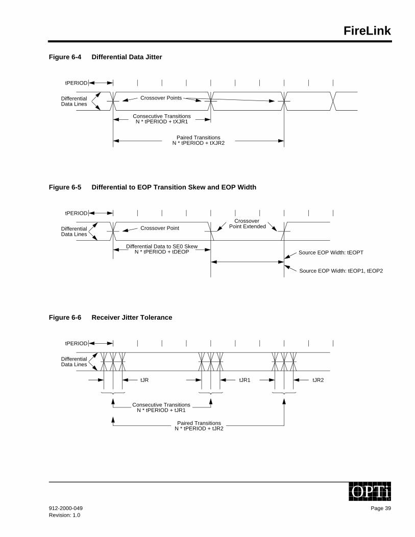
FireLink
912-2000-049 Page 39Revision: 1.0
OPTi®
Figure 6-4 Differential Data Jitter
Figure 6-5 Differential to EOP Transition Skew and EOP Width
Figure 6-6 Receiver Jitter Tolerance
tPERIOD
DifferentialData Lines
Consecutive TransitionsN * tPERIOD + tXJR1
Paired TransitionsN * tPERIOD + tXJR2
Crossover Points
tPERIOD
DifferentialData Lines
Differential Data to SE0 SkewN * tPERIOD + tDEOP
Crossover PointCrossover
Point Extended
Source EOP Width: tEOPT
Source EOP Width: tEOP1, tEOP2
tPERIOD
DifferentialData Lines
Consecutive TransitionsN * tPERIOD + tJR1
tJR tJR1 tJR2
Paired TransitionsN * tPERIOD + tJR2

FireLink
Page 40 912-3000-049Revision: 1.0
OPTi®

FireLink
912-2000-049 Page 41Revision: 1.0
OPTi®
7.0 Mechanical Package Outlines
Figure 7-1 100-Pin Low-Profile Quad Flat Pack (LQFP)
EHe

FireLink
Page 42 912-3000-049Revision: 1.0
OPTi®
Figure 7-2 100-Pin Quad Flat Pack (QFP)

FireLink
912-2000-049 Page 43Revision: 1.0
OPTi®
8.0 NAND Tree Test ModeThe NAND tree mode tests both input and bi-directional pins that are part of the NAND tree chain. The NAND tree chain startsat pin 13 (VD1+) while the output of the chain is at pin 24 (PWRON2). To use the NAND tree test mode, strap FireLink 1.0 bypulling up the following pins during the rising edge of RESET#: Pin 1 (A20_out), Pin 25 (TEST1) and Pin 21 (TEST0). For reli-able strapping, toggle PCICLK at least two times after RESET# goes low, and at least two times after RESET# goes high. Afterthat strapping sequence, set both RESET# and PCICLK high. Do not toggle RESET# and PCICLK during the NAND tree test.See the tables below for the NAND tree test mode pins.
Revision 1.013 VD1+
(NAND input
start)18 VD2+
6 USBCLK
9 POWERON1
10 PWRFLT1
11 PWRGD1
21 TEST0(Strap option: high = NAND testmode)
22 PWRGD2
23 PWRFLT2
25 TEST1(Strap option: high = NAND testmode)
31 RESET#(held high duringduring test)
32 PCICLK (held high duringduring test)
35 GNT#
37 AD31
38 AD30
39 AD29
42 AD28
43 AD27
44 AD26
45 AD25
46 CLKRUN#
48 AD24
49 C/BE3#
50 IDSEL
51 AD23
52 AD22
55 AD21
56 AD20
57 AD19
58 AD18
61 AD17
62 AD16
63 C/BE2#
64 FRAME#
67 IRDY#
68 TRDY#
69 DEVSEL#
70 STOP#
71 PERR#
73 ITQ12
76 PAR
77 C/BE1#
78 AD15
79 AD14
82 AD13
83 AD12
84 AD11
86 AD10
87 AD9
88 AD8
89 C/BE0#
93 AD7
94 AD6
95 AD5
97 IRQ1_in
99 AD4
100
AD3
1 A20_out(Strap option: high = NAND testmode)
2 AD2
3 AD1
4 AD0
24 PWRON2 (NAND Output)

FireLink
Page 44 912-3000-049Revision: 1.0
OPTi®

FireLink
912-2000-049 Page 45Revision: 1.0
OPTi®
HEADQUARTERS:OPTi Inc.888 Tasman DriveMilpitas, CA 95035tel:408-486-8000fax:408-486-8011
SALES OFFICES:JapanOPTi Japan KKMurata Building 6F, 2-22-7Ohhashi Meguro-kuTokyo 153, Japantel:81-3-5454-0178fax:81-3-5454-0168
TaiwanOPTi Inc. 9F, No 303, Sec 4, Hsin YihRoadTaipei, Taiwan, ROCtel:886-2-2-325-8520fax:886-2-2-325-6520

OPTi Inc.888 Tasman DriveMilpitas, CA 95035Tel: (408) 486-8000Fax: (408) 486-8001
WWW: http://www.opti.com/