Embed Size (px)
Citation preview
Journal of Engineering Science and Technology Vol. 9, No. 1 (2014) 47 - 63 © School of Engineering, Taylor’s University
47
FINITE ELEMENT ANALYSIS ON THE EFFECT OF SOLDER JOINT GEOMETRY FOR THE RELIABILITY OF BALL GRID ARRAY ASSEMBLY WITH FLEXIBLE AND RIGID PCBS
CHUN-SEAN LAU*, M. Z. ABDULLAH, M. ABDUL MUJEEBU, N. MD. YUSOP
School of Mechanical Engineering, Universiti Sains Malaysia, Engineering Campus,
14300 Nibong Tebal, Penang, Malaysia
*Corresponding Author: [email protected]
Abstract
In the present study, three-dimensional (3D) finite element simulation on 132
PIN fleXBGATM package was performed to predict the effect of solder joint
geometry on the reliability of Ball Grid Array (BGA) solder joints on flexible and rigid PCBs subjected to thermo-cyclic loading. The commercial FEA tool
ABAQUS Version 6.9 was used for the simulations of various shapes of solder
joints such as barrel, column and hourglass. Apart from a global modeling, the
submodeling analysis technique (local modeling) was also used on the critically
affected solder joints, in order to enhance the computation efficiency. The
accumulated creep strain and strain energy density were observed for each case, and optimum geometries were obtained. The model was validated with the
published experimental data with the minimum percentage error of 3%. It was
observed that the hourglass solder joint geometry was very crucial on the
reliability of BGA solder joints, and for a given PCB, the optimal choice of
hourglass solder joint geometry depended on its rigidity.
Keywords: Finite element simulation, Ball grid array (BGA), Solder joint geometry,
Flexible PCB, Submodeling analysis technique.
1. Introduction
Tin-based eutectic and lead-free solder joints are used in the ball grid array (BGA)
packages to ensure electrical and mechanical functionalities between the packages and
the PCB [1-2]. Alternating strains and stresses caused by mismatch of coefficient of
thermal expansion are the main causes of failure in solder joint interconnections.
Several factors have been found to be affecting the solder joint reliability, such
as solder joint geometry, board material, chip size, interface metallurgy, and underfill
48 C.-S. Lau et al.
Journal of Engineering Science and Technology February 2014, Vol. 9(1)
Nomenclatures
A Power Law multiplier, s-1
B Hyperbolic law multiplier, MPa-1
D Pad diameter, mm
H Standoff height of the solder joint, mm
M Midpoint diameter of solder joint, mm
n Stress order
R Universal gas constant, J/mol.K
VT Volume of barrel-shaped solder joint, mm3
Ux,
Uy, Uz
Velocity component in x, y, z directions, mm/s
Greek Symbols
∆� Activation energy, J/mol
∆W Accumulated strain energy density per cycle of each element, MPa
∆Wave Average accumulated strain energy density per cycle for the
interface elements, PSI
∆Wmax Accumulated strain energy density per cycle of critical element, MPa
���� Equivalent strains
Ө Temperature of thermal load, K
Ө� User-defined value of absolute zero on the temperature scale used, K
�� Equivalent stresses, MPa
Fatigue life, cycles
Φc Diameter of copper pad, mm
Φs Diameter of midpoint solder joint, mm
and substrate materials [3]. However, very little work is found in the open
literature, on the solder joint reliability analysis of flexible electronics [4]. The
flexible printed circuit board (FPCB) has unique capabilities including reduced
board thickness, added “twist” of flexibility and vibration resistance. This
lightness, and ability to bend to various shapes, make FPCB play vital role in
electronic product miniaturization and replace rigid boards (RPCB) in numerous
electronic devices [4].
Liu and Lu [5] found that solder joint geometry characterized by shape and
standoff height is the dominant factor affecting solder joint reliability. Several
approaches, such as stacked solder, double bump technology, stretched solder,
ceramic column grid array and second-reflow-process approach [6] were reported
to increase the standoff height and control the shape of solder bump connection.
The stacked solder technique used the bump-limiting metal pads to separate
solder bump at different level by sequential stacking process [7]. Double bump
technology entailed the controlled overlapping of two molten solder bumps on
both surfaces to form nearly cylindrical joint [8]. A mechanical standoff was used
in this technique to control the final separation between packages and PCB. A
cost effective stretch solder joint involved the process of stretching the solder
joint to acquire hourglass shape and greater standoff height [9]. Liu and Lu [5]
Finite Element Analysis on the Effect of Solder Joint Geometry �. 49
Journal of Engineering Science and Technology February 2014, Vol. 9(1)
demonstrated that hourglass shape solders had the lowest plastic strain and better
reliability during thermal cycling. For the constant solder volume and pad size,
hourglass-shaped solder joint had the greatest standoff height, followed by
column and barrel shaped solder joint.
Accelerated thermal cycling (ATC) tests have been widely used in the
electronics industry to assess the reliability of new electronic products against the
low-cycle fatigue in field environment [10]. However, this test method is expensive
and time consuming. With the maturity of numerical techniques, the failure of
solder joints could easily be predicted by simulations without resorting to lengthy
and costly tests. Over the past decades, the validity of finite element analysis (FEA)
has been discussed by many researchers [11-13]. Ridout and Bailey [10] reviewed
various modeling methods to predict solder joint failure, such as analytical method,
constitutive law plus fatigue law methods, and damage mechanics based methods
[14]. The analytical method proposed by Engelmaier [15] for predicting the lifetime
of 63Sn37Pb joints was recommended in the IPC-D-279 standard. The damage
mechanics based methods allowed crack paths to be predicted. A review of
covering several methods has provided by Desai and Whitenack [16].
Constitutive law plus fatigue law methods work by running transient
simulation with FEM tools such as MSC/NASTRAN, ANSYS or ABAQUS to
predict the solder’s stress strain behavior during a thermal cycle. The standard
method for FEA of solder joints involves only the modeling of steady-state creep,
which could provide a reasonable prediction. Many authors [17] have used
hyperbolic sine creep to capture the change in creep mechanism. Darveaux et al.
[18] have published constants for four different alloys including SnPb and
Sn3.5Ag. From this prediction, either the accumulated effective plastic strain per
cycle or the accumulated strain energy density per cycle of each element (∆W)
was extracted to be used in a fatigue law. Lee et al. [19] reviewed various fatigue
laws; the simplest fatigue laws were the Coffin–Manson law and the strain energy
based law, used by Akay et al. [11]. Darveaux [20] fatigue law predicted the time
taken for crack initiation, and crack propagation rate by averaging ∆W over a
layer of solder 25 µm thick adjacent to the package interface where the cracks
were expected to develop.
As far as the authors are aware, the effect of solder joint geometry on the
reliability of BGA solder joints on FPCB has less reported so far [21-23].
Accordingly, in the present study, three-dimensional (3D) finite element simulation
on 132-PIN fleXBGATM package is performed considering both FPCB and RPCB
[24-25]. The commercial FEA tool ABAQUS Version 6.9 is used for the
simulations of various shapes of solder joints such as barrel, column and hourglass.
Furthermore, the submodeling analysis technique [26] is used to enhance the
computation efficiency. The accumulated creep strain and strain energy density are
observed for each case, and optimum geometries are obtained. The model is
validated with the published experimental data [24] with acceptable error.
2. Materials and Methods
2.1. Package dimensions
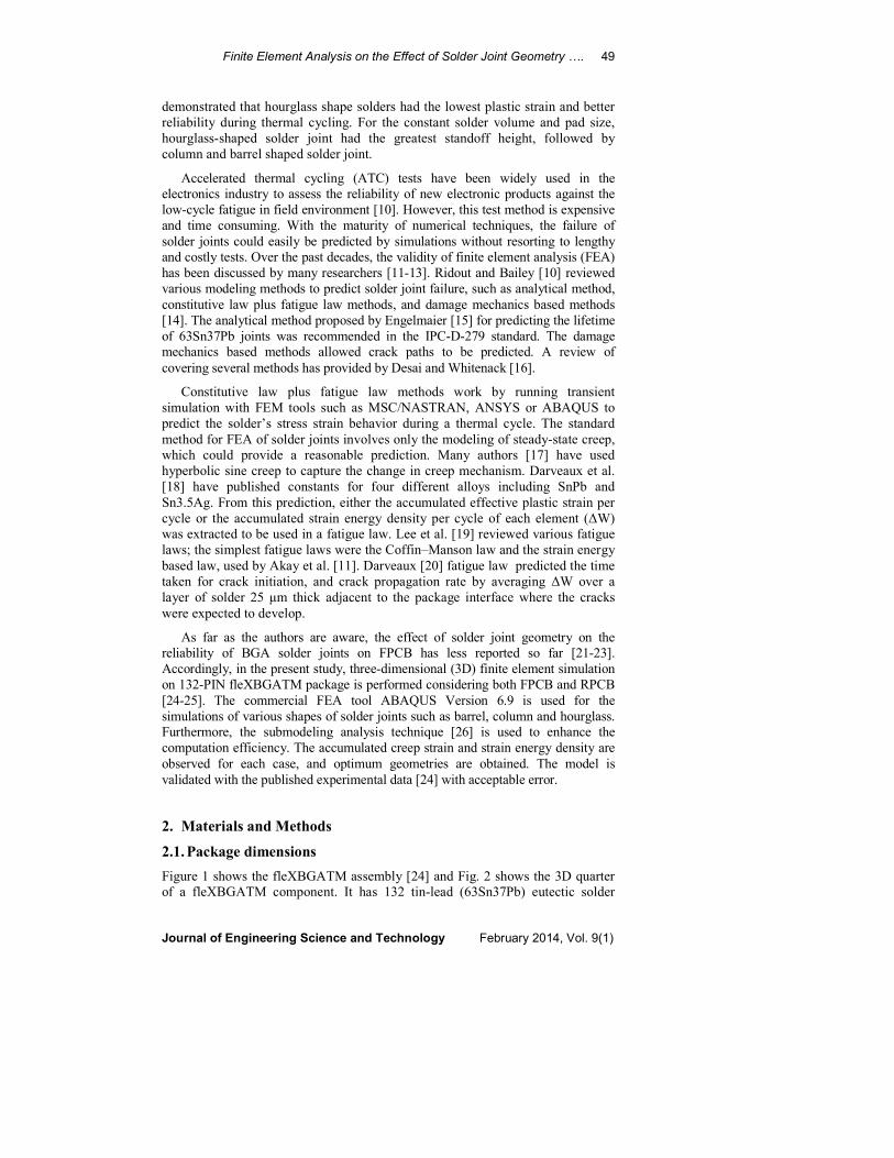
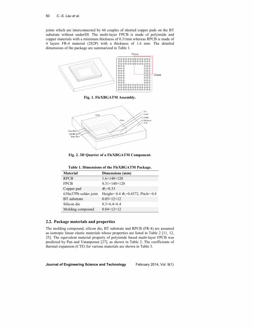
Figure 1 shows the fleXBGATM assembly [24] and Fig. 2 shows the 3D quarter
of a fleXBGATM component. It has 132 tin-lead (63Sn37Pb) eutectic solder
50 C.-S. Lau et al.
Journal of Engineering Science and Technology February 2014, Vol. 9(1)
joints which are interconnected by 66 couples of shorted copper pads on the BT
substrate without underfill. The multi-layer FPCB is made of polyimide and
copper materials with a minimum thickness of 0.31mm whereas RPCB is made of
4 layers FR-4 material (2S2P) with a thickness of 1.6 mm. The detailed
dimensions of the package are summarized in Table 1.
Fig. 1. FleXBGATM Assembly.
Fig. 2. 3D Quarter of a FleXBGATM Component.
Table 1. Dimensions of the FleXBGATM Package.
Material Dimensions (mm)
RPCB 1.6×140×120
FPCB 0.31×140×120
Copper pad Φc=0.33
63Sn37Pb solder joint Height= 0.4 Φs=0.4572, Pitch= 0.8
BT substrate 0.05×12×12
Silicon die 0.3×6.4×6.4
Molding compound 0.84×12×12
2.2. Package materials and properties
The molding compound, silicon die, BT substrate and RPCB (FR-4) are assumed
as isotropic linear elastic materials whose properties are listed in Table 2 [11, 12,
25]. The equivalent material property of polyimide based multi-layer FPCB was
predicted by Pan and Vatanporast [27], as shown in Table 2. The coefficients of
thermal expansion (CTE) for various materials are shown in Table 3.
Finite Element Analysis on the Effect of Solder Joint Geometry �. 51
Journal of Engineering Science and Technology February 2014, Vol. 9(1)
Table 2. Properties of Constituent Materials.
Table 3. Coefficient of Thermal Expansion (CTE) for Various Solders.
Material Temperature (K) CTE (ppm/K)
63Sn37Pb [1] 293 24.0
423 26.9
FPCB: Polyimide [27] - 26.1
RPCB: FR-4 [25] - 15
BT Substrate [11] - 15
Silicon [12] - 2.5
Molding Compound [12] - 14.8
Since the solder temperature is assumed to be above half of its melting point,
time-dependent creep processes are expected to dominate the deformation
kinetics. A hyperbolic sine creep law [1, 16] is used to study the evolution and
accumulation of irreversible strains and energies of solder joints made of various
types of solder:
���� = �(sinh���)� exp�(−
∆�
�(Ө�Ө�)) (1)
where ����� is equivalent strains, ��� is equivalent stresses, θ is the
temperature, θ z, the user-defined value of absolute zero on the temperature scale
used, R is the universal gas constant, A is Power Law multiplier, B is hyperbolic
law multiplier, n is the stress order and ∆� is the activation energy. Besides, A, B,
n and ∆� represent the characteristics for the secondary creep behavior of a
particular solder. The values A, B, n and ∆� and R for the 63Sn37Pb solder used
in the present study are listed in Table 4 [1].
Note that this type of creep constitutive equation ignores transient creep
effects and assumes steady-state creep after the beginning of loading. This might
be deficient in studying creep under thermal stress reversals. Besides, for thermal
load cycles with a period of 3600s, the creep dominates and the instantaneous
time-independent plasticity is assumed as insignificant; this would suggest that
the common practice of ignoring instantaneous plasticity is justified [10].
Table 4. Creep Law Constants of Various Solders [1].
Solder A (s-1
) B (MPa-1
) n ∆�(J/mol) R (J/mol.K)
63Sn37Pb 96200 0.086956 3.3 67390 8.314
Material Young’s Modulus
(MPa)
Poisson’s
ratio
PCB
FPCB: Polyimide [27] 5225 0.25
RPCB: FR-4 [25] 18200 0.25
Leaded
Solder 63Sn37Pb [1]
23250 (373K) 0.36 (373K)
19000 (423K) 0.36 (423K)
Substrate BT Substrate [11] 26000 0.39
Die Silicon [12] 130360 0.28
Mold Molding Compound [12] 16520 0.25
52 C.-S. Lau et al.
Journal of Engineering Science and Technology February 2014, Vol. 9(1)
2.3. FEA modelling
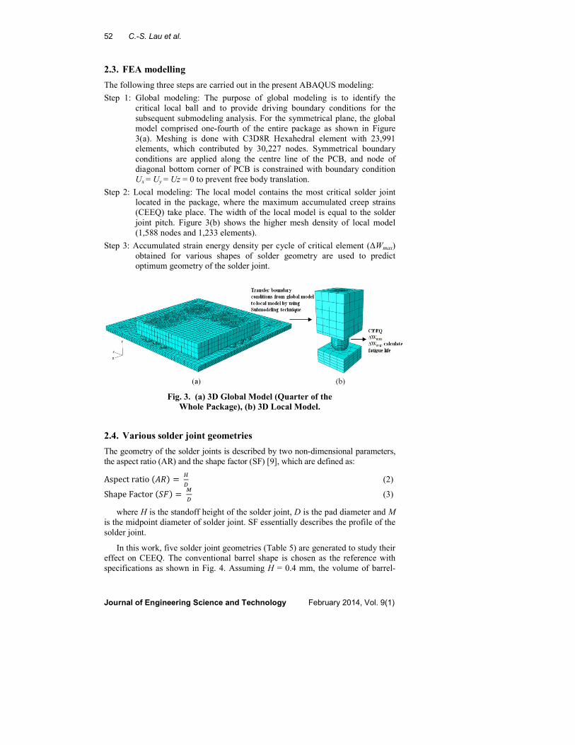
The following three steps are carried out in the present ABAQUS modeling:
Step 1: Global modeling: The purpose of global modeling is to identify the
critical local ball and to provide driving boundary conditions for the
subsequent submodeling analysis. For the symmetrical plane, the global
model comprised one-fourth of the entire package as shown in Figure
3(a). Meshing is done with C3D8R Hexahedral element with 23,991
elements, which contributed by 30,227 nodes. Symmetrical boundary
conditions are applied along the centre line of the PCB, and node of
diagonal bottom corner of PCB is constrained with boundary condition
Ux = Uy = Uz = 0 to prevent free body translation.
Step 2: Local modeling: The local model contains the most critical solder joint
located in the package, where the maximum accumulated creep strains
(CEEQ) take place. The width of the local model is equal to the solder
joint pitch. Figure 3(b) shows the higher mesh density of local model
(1,588 nodes and 1,233 elements).
Step 3: Accumulated strain energy density per cycle of critical element (∆Wmax)
obtained for various shapes of solder geometry are used to predict
optimum geometry of the solder joint.
Fig. 3. (a) 3D Global Model (Quarter of the
Whole Package), (b) 3D Local Model.
2.4. Various solder joint geometries
The geometry of the solder joints is described by two non-dimensional parameters,
the aspect ratio (AR) and the shape factor (SF) [9], which are defined as:
Aspect�ratio�(�%) = ��
& (2)
Shape�Factor�()*) = �+
& (3)
where H is the standoff height of the solder joint, D is the pad diameter and M
is the midpoint diameter of solder joint. SF essentially describes the profile of the
solder joint.
In this work, five solder joint geometries (Table 5) are generated to study their
effect on CEEQ. The conventional barrel shape is chosen as the reference with
specifications as shown in Fig. 4. Assuming H = 0.4 mm, the volume of barrel-
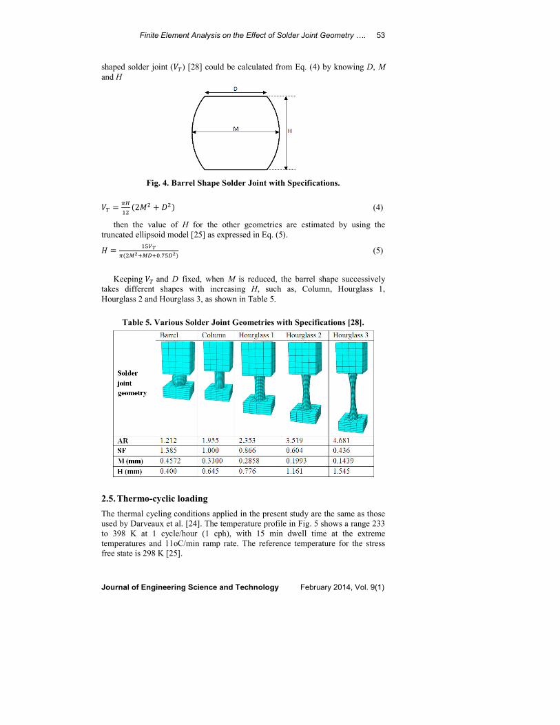
Finite Element Analysis on the Effect of Solder Joint Geometry �. 53
Journal of Engineering Science and Technology February 2014, Vol. 9(1)
shaped solder joint (,-) [28] could be calculated from Eq. (4) by knowing D, M
and H
Fig. 4. Barrel Shape Solder Joint with Specifications.
,- =.�
/0(220 + 40) (4)
then the value of H for the other geometries are estimated by using the
truncated ellipsoid model [25] as expressed in Eq. (5).
� =/567
.(0+89+&9:.<5&8) (5)
Keeping ,- and D fixed, when M is reduced, the barrel shape successively
takes different shapes with increasing H, such as, Column, Hourglass 1,
Hourglass 2 and Hourglass 3, as shown in Table 5.
Table 5. Various Solder Joint Geometries with Specifications [28].
2.5. Thermo-cyclic loading
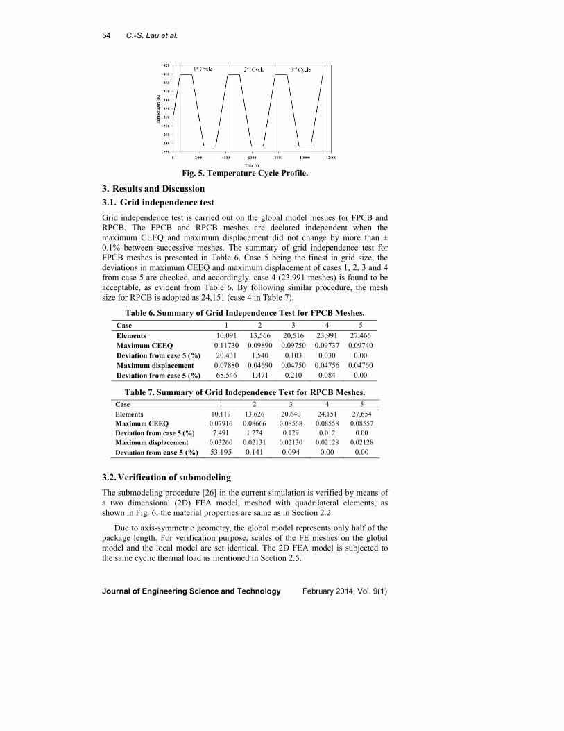
The thermal cycling conditions applied in the present study are the same as those
used by Darveaux et al. [24]. The temperature profile in Fig. 5 shows a range 233
to 398 K at 1 cycle/hour (1 cph), with 15 min dwell time at the extreme
temperatures and 11oC/min ramp rate. The reference temperature for the stress
free state is 298 K [25].
54 C.-S. Lau et al.
Journal of Engineering Science and Technology February 2014, Vol. 9(1)
Fig. 5. Temperature Cycle Profile.
3. Results and Discussion
3.1. Grid independence test
Grid independence test is carried out on the global model meshes for FPCB and
RPCB. The FPCB and RPCB meshes are declared independent when the
maximum CEEQ and maximum displacement did not change by more than ±
0.1% between successive meshes. The summary of grid independence test for
FPCB meshes is presented in Table 6. Case 5 being the finest in grid size, the
deviations in maximum CEEQ and maximum displacement of cases 1, 2, 3 and 4
from case 5 are checked, and accordingly, case 4 (23,991 meshes) is found to be
acceptable, as evident from Table 6. By following similar procedure, the mesh
size for RPCB is adopted as 24,151 (case 4 in Table 7).
Table 6. Summary of Grid Independence Test for FPCB Meshes.
Table 7. Summary of Grid Independence Test for RPCB Meshes.
3.2. Verification of submodeling
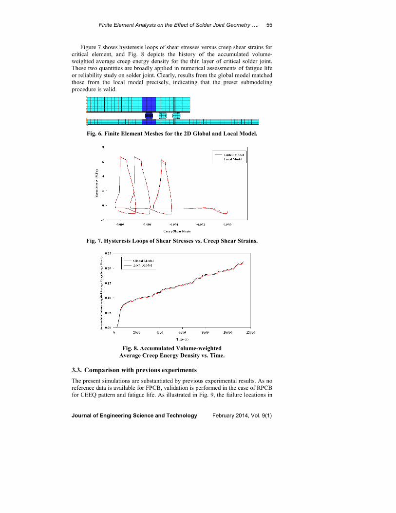
The submodeling procedure [26] in the current simulation is verified by means of
a two dimensional (2D) FEA model, meshed with quadrilateral elements, as
shown in Fig. 6; the material properties are same as in Section 2.2.
Due to axis-symmetric geometry, the global model represents only half of the
package length. For verification purpose, scales of the FE meshes on the global
model and the local model are set identical. The 2D FEA model is subjected to
the same cyclic thermal load as mentioned in Section 2.5.
Case 1 2 3 4 5
Elements 10,091 13,566 20,516 23,991 27,466
Maximum CEEQ 0.11730 0.09890 0.09750 0.09737 0.09740
Deviation from case 5 (%) 20.431 1.540 0.103 0.030 0.00
Maximum displacement 0.07880 0.04690 0.04750 0.04756 0.04760
Deviation from case 5 (%) 65.546 1.471 0.210 0.084 0.00
Case 1 2 3 4 5
Elements 10,119 13,626 20,640 24,151 27,654
Maximum CEEQ 0.07916 0.08666 0.08568 0.08558 0.08557
Deviation from case 5 (%) 7.491 1.274 0.129 0.012 0.00
Maximum displacement 0.03260 0.02131 0.02130 0.02128 0.02128
Deviation from case 5 (%) 53.195 0.141 0.094 0.00 0.00
Finite Element Analysis on the Effect of Solder Joint Geometry �. 55
Journal of Engineering Science and Technology February 2014, Vol. 9(1)
Figure 7 shows hysteresis loops of shear stresses versus creep shear strains for
critical element, and Fig. 8 depicts the history of the accumulated volume-
weighted average creep energy density for the thin layer of critical solder joint.
These two quantities are broadly applied in numerical assessments of fatigue life
or reliability study on solder joint. Clearly, results from the global model matched
those from the local model precisely, indicating that the preset submodeling
procedure is valid.
Fig. 6. Finite Element Meshes for the 2D Global and Local Model.
Fig. 7. Hysteresis Loops of Shear Stresses vs. Creep Shear Strains.
Fig. 8. Accumulated Volume-weighted
Average Creep Energy Density vs. Time.
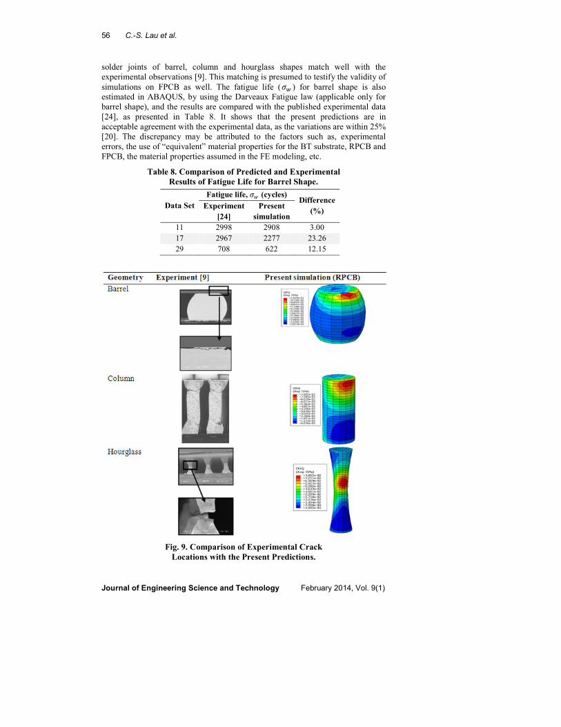
3.3. Comparison with previous experiments
The present simulations are substantiated by previous experimental results. As no
reference data is available for FPCB, validation is performed in the case of RPCB
for CEEQ pattern and fatigue life. As illustrated in Fig. 9, the failure locations in
56 C.-S. Lau et al.
Journal of Engineering Science and Technology February 2014, Vol. 9(1)
solder joints of barrel, column and hourglass shapes match well with the
experimental observations [9]. This matching is presumed to testify the validity of
simulations on FPCB as well. The fatigue life ( ) for barrel shape is also
estimated in ABAQUS, by using the Darveaux Fatigue law (applicable only for
barrel shape), and the results are compared with the published experimental data
[24], as presented in Table 8. It shows that the present predictions are in
acceptable agreement with the experimental data, as the variations are within 25%
[20]. The discrepancy may be attributed to the factors such as, experimental
errors, the use of “equivalent” material properties for the BT substrate, RPCB and
FPCB, the material properties assumed in the FE modeling, etc.
Table 8. Comparison of Predicted and Experimental
Results of Fatigue Life for Barrel Shape.
Fig. 9. Comparison of Experimental Crack
Locations with the Present Predictions.
Data Set
Fatigue life, = (cycles) Difference
(%) Experiment
[24]
Present
simulation
11 2998 2908 3.00
17 2967 2277 23.26
29 708 622 12.15
Finite Element Analysis on the Effect of Solder Joint Geometry �. 57
Journal of Engineering Science and Technology February 2014, Vol. 9(1)
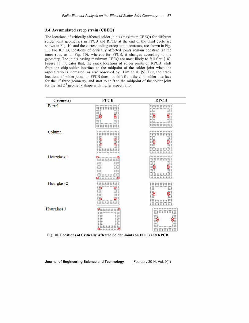
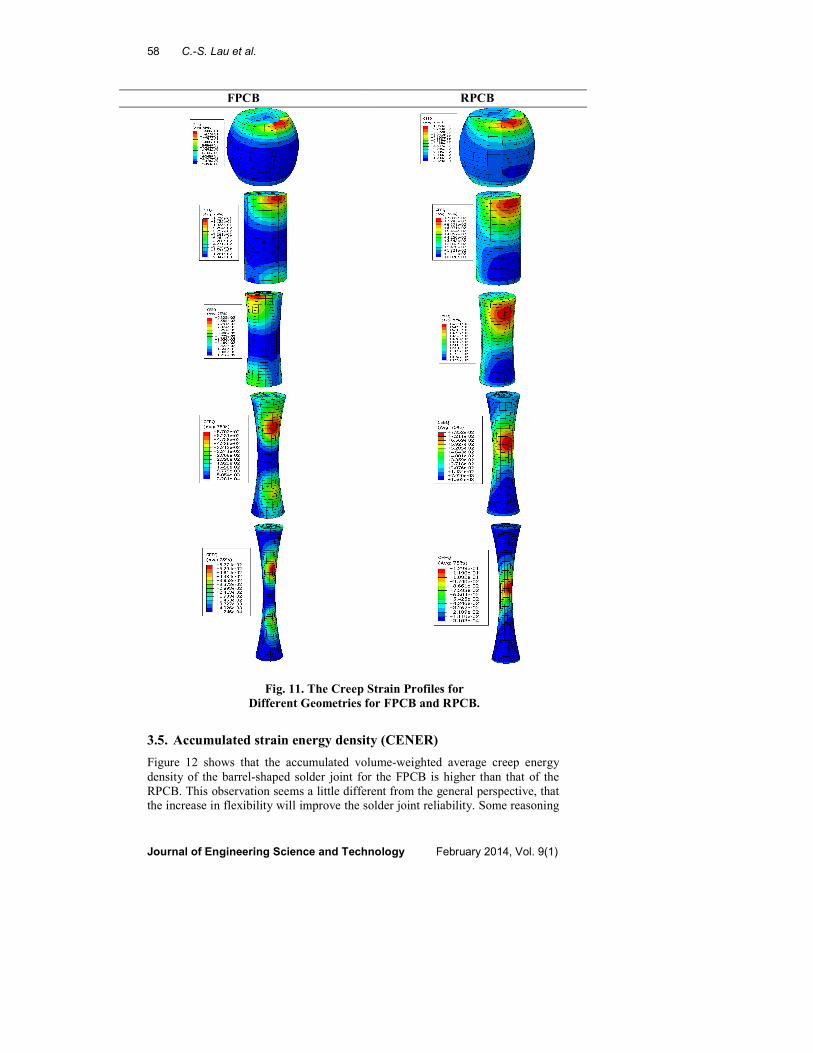
3.4. Accumulated creep strain (CEEQ)
The locations of critically affected solder joints (maximum CEEQ) for different
solder joint geometries in FPCB and RPCB at the end of the third cycle are
shown in Fig. 10, and the corresponding creep strain contours, are shown in Fig.
11. For RPCB, locations of critically affected joints remain constant (at the
inner row, as in Fig. 10), whereas for FPCB, it changes according to the
geometry. The joints having maximum CEEQ are most likely to fail first [18].
Figure 11 indicates that, the crack locations of solder joints on RPCB shift
from the chip-solder interface to the midpoint of the solder joint when the
aspect ratio is increased, as also observed by Lim et al. [9]. But, the crack
locations of solder joints on FPCB does not shift from the chip-solder interface
for the 1st three geometry, and start to shift to the midpoint of the solder joint
for the last 2rd
geometry shape with higher aspect ratio.
Fig. 10. Locations of Critically Affected Solder Joints on FPCB and RPCB.
58 C.-S. Lau et al.
Journal of Engineering Science and Technology February 2014, Vol. 9(1)
FPCB RPCB
Fig. 11. The Creep Strain Profiles for
Different Geometries for FPCB and RPCB.
3.5. Accumulated strain energy density (CENER)
Figure 12 shows that the accumulated volume-weighted average creep energy
density of the barrel-shaped solder joint for the FPCB is higher than that of the
RPCB. This observation seems a little different from the general perspective, that
the increase in flexibility will improve the solder joint reliability. Some reasoning
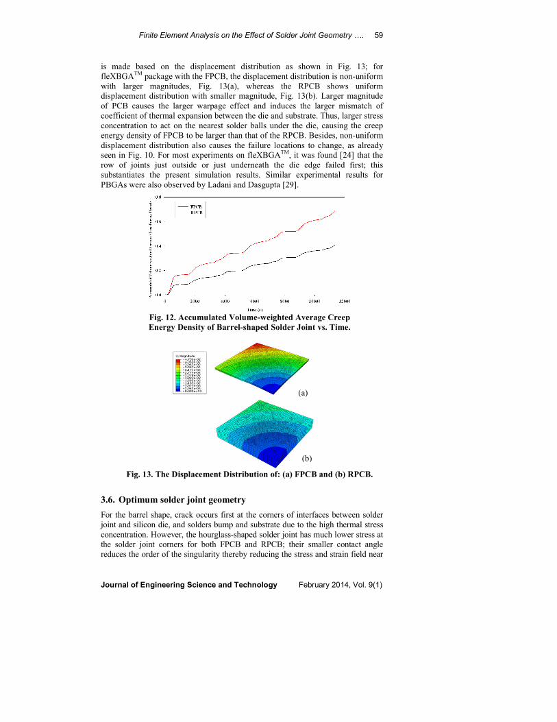
Finite Element Analysis on the Effect of Solder Joint Geometry �. 59
Journal of Engineering Science and Technology February 2014, Vol. 9(1)
is made based on the displacement distribution as shown in Fig. 13; for
fleXBGATM
package with the FPCB, the displacement distribution is non-uniform
with larger magnitudes, Fig. 13(a), whereas the RPCB shows uniform
displacement distribution with smaller magnitude, Fig. 13(b). Larger magnitude
of PCB causes the larger warpage effect and induces the larger mismatch of
coefficient of thermal expansion between the die and substrate. Thus, larger stress
concentration to act on the nearest solder balls under the die, causing the creep
energy density of FPCB to be larger than that of the RPCB. Besides, non-uniform
displacement distribution also causes the failure locations to change, as already
seen in Fig. 10. For most experiments on fleXBGATM
, it was found [24] that the
row of joints just outside or just underneath the die edge failed first; this
substantiates the present simulation results. Similar experimental results for
PBGAs were also observed by Ladani and Dasgupta [29].
Fig. 12. Accumulated Volume-weighted Average Creep
Energy Density of Barrel-shaped Solder Joint vs. Time.
Fig. 13. The Displacement Distribution of: (a) FPCB and (b) RPCB.
3.6. Optimum solder joint geometry
For the barrel shape, crack occurs first at the corners of interfaces between solder
joint and silicon die, and solders bump and substrate due to the high thermal stress
concentration. However, the hourglass-shaped solder joint has much lower stress at
the solder joint corners for both FPCB and RPCB; their smaller contact angle
reduces the order of the singularity thereby reducing the stress and strain field near
(a)
(b)
60 C.-S. Lau et al.
Journal of Engineering Science and Technology February 2014, Vol. 9(1)
contact edges. Moreover, the hourglass shape contributes to protecting the weak
interfaces between the solder joint and the substrate, by allowing the CEEQ to move
towards the middle. It was established by tensile and shear tests that that hourglass-
shaped solder joint had high adhesion stress than barrel-shaped solder joint, and
failed at or close to midpoint while barrel-shape failed at the interface [7].
It should be noted that, for a given solder joint volume, the advantage of protecting
the weak interface by increasing the aspect ratio is countered by the threat of midpoint
failure. Moreover, increasing the solder joint height without affecting the solder joint
pitch is restricted by I/O density and cost. This situation calls for optimum solder joint
geometry in terms of aspect ratio, strain distribution pattern and cost.
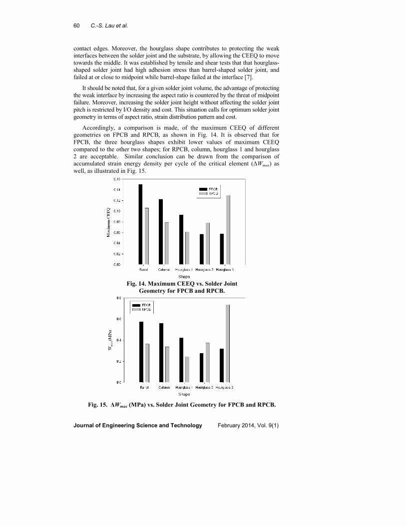
Accordingly, a comparison is made, of the maximum CEEQ of different
geometries on FPCB and RPCB, as shown in Fig. 14. It is observed that for
FPCB, the three hourglass shapes exhibit lower values of maximum CEEQ
compared to the other two shapes; for RPCB, column, hourglass 1 and hourglass
2 are acceptable. Similar conclusion can be drawn from the comparison of
accumulated strain energy density per cycle of the critical element (∆Wmax) as
well, as illustrated in Fig. 15.
Fig. 14. Maximum CEEQ vs. Solder Joint
Geometry for FPCB and RPCB.
Fig. 15. ∆Wmax (MPa) vs. Solder Joint Geometry for FPCB and RPCB.
Finite Element Analysis on the Effect of Solder Joint Geometry �. 61
Journal of Engineering Science and Technology February 2014, Vol. 9(1)
4. Conclusions
In the present study three-dimensional (3D) finite element simulation on 132-PIN
fleXBGATM package is performed to predict the effect of solder joint geometry on
the reliability of BGA solder joints on flexible and rigid PCBs. The commercial
FEA tool ABAQUS Version 6.9 is used for the simulations of various shapes of
solder joints such as barrel, column and hourglass. The model is well validated with
the published experimental data. From the global and local modeling and
simulations, it is observed that the solder joint geometry significantly influences the
reliability of BGA solder joints, and for a given PCB, the choice of solder joint
geometry depends on its rigidity. It is also found that as the geometry changes; the
locations of critically affected joints do not change on RPCB, but change on FPCB.
For future work, experiments may be performed to confirm the present simulation
results on FPCB. Study on the effects of solder materials (both leaded and lead-free)
on the reliability of different types of geometries will also be interesting.
Acknowledgements
The authors would like to thank Universiti Sains Malaysia for the financial support
for this research work.
References
1. Hannach, T.; Worrack, H.; Muller, W.H.; and Hauck, T. (2009). Creep in
microelectronic solder joints: finite element simulations versus semi-
analytical methods. Archive of Applied Mechanics, 79(6), 605-617.
2. Qian, Z.F.; and Liu, S. (1998). On the life prediction and accelerated testing
of solder joints. International Journal of Microcircuits and Electronic
Packaging, 22(4), 288-304.
3. Peng, C.T.; Chiang, K.N.; Ku, T.; and Chang, K. (2004). Design, fabrication and
comparison of lead-free/eutectic solder joint reliability of flip chip package.
Proceedings of the 5th International Conference in Thermal and Mechanical
Simulation and Experiments in Microelectronics and Microsystems.
4. Arruda, L.; Bonadiman R.; Costa, J.; and Reinikainen, T. (2009). Cracking
phenomena on flexible-rigid interfaces in PCBs under thermo cycling
loading. Circuit World, 35(2), 18-22.
5. Liu, X.S.; and Lu, G.Q. (2003). Effects of solder joint shape and height on
thermal fatigue lifetime. IEEE Transactions on Components and Packaging
Technologies, 26(2), 455-465.
6. Chiang, K.N.; Lin, Y.T.; and Cheng, H.C. (2000). On enhancing eutectic
solder joint reliability using a second-reflow-process approach. IEEE
Transactions on Advanced Packaging, 23(1), 9-14.
7. Lu, G.Q.; Liu, X.S.; Wen, S.H.; Calata, J.N.; and Bai, J.G. (2004). Strategies
for improving the reliability of solder joints on power semiconductor devices.
Soldering & Surface Mount Technology, 16(2), 27-40.
8. Frank, L.; and Oien, M.A. (1988). Double-bump surface-mount technology
for very high IO interconnections. Fourth IEEE/CHMT European
International in Electronic Manufacturing Technology Symposium.
62 C.-S. Lau et al.
Journal of Engineering Science and Technology February 2014, Vol. 9(1)
9. Lim, S.S.; Rajoo, R.; Wong, E.H.; and Hnin, W.Y. (2006). Reliability
performance of stretch solder interconnections. 31st International Conference
in Electronics Manufacturing and Technology.
10. Ridout, S.; and Bailey, C. (2007). Review of methods to predict solder joint
reliability under thermo-mechanical cycling. Fatigue & Fracture of
Engineering Materials & Structures, 30(5), 400-412.
11. Akay, H.U.; Liu Y.; and Rassaian, M. (2003). Simplification of finite element
models for thermal fatigue life prediction of PBGA packages. Journal of
Electronic Packaging, 125(3), 347-353.
12. Yang, Q.J.; Shi, X.Q.; Wang, Z.P.; and Shi, Z.F. (2003). Finite-element
analysis of a PBGA assembly under isothermal/mechanical twisting loading.
Finite Elements in Analysis and Design, 39(9), 819-833.
13. Dare, A.A.; and Petinrin, M.O. (2010). Modelling of natural convection
along isothermal plates and in channels using diffusion velocity method.
Maejo International Journal of Science and Technology, 4(01), 43-52.
14. Abdul-Baqi, A.; Schreurs, P.J.G.; and Geers, M.G.D. (2005). Fatigue damage
modeling in solder interconnects using a cohesive zone approach.
International Journal of Solids and Structures, 42(3-4), 927-942.
15. Engelmaier, W. (1991). Solder joint reliability: Theory and applications
(Edited by J. H. Lau). New York.
16. Desai, C.S.; and Whitenack, R. (2001). Review of models and the disturbed
state concept for thermomechanical analysis in electronic packaging. Journal
of Electronic Packaging, 123(1), 19-33.
17. Lee, H.K.; Lee, S.M.; Soo, Y.F.; and Wong, S.J. (2006). Improving solder
joint reliability of WLP by means of a compliant layer. 31st International
Conference in Electronics Manufacturing and Technology.
18. Darveaux, R.; Banerji, K.; Mawer, A.; and Doddy, G. (1995). Reliability of
plastic ball grid array assembly in ball grid array technology (Edited by J.
H. Lau). New York.
19. Lee, W.W.; Nguyen, L.T.; and Selvaduray, G.S. (2000). Solder joint fatigue
models: review and applicability to chip scale packages. Microelectronics
Reliability, 40(2), 231-244.
20. Darveaux, R. (2000). Effect of simulation methodology on solder joint crack
growth correlation. Proceedings of 50th Electronic Components and
Technology Conference.
21. Wu, Z.H. (2012). The modeling and prediction study of BLP device solder
joint three-dimensional shape. Applied Mechanics and Materials, 121-126,
2338-2342.
22. Amalu, E.H.; and Ekere, N.N. (2012). High temperature reliability of lead-
free solder joints in a flip chip assembly. Journal of Materials Processing
Technology, 212(2), 471-483.
23. Wei, H.; and Wang, K. (2011). A probabilistic approach to predict thermal
fatigue life for ball grid array solder joints. Journal of Electronic Materials,
40(11), 2314-2319.
24. Darveaux, R.; Heckman, J.; Syed, A.; and Mawer, A. (2000). Solder joint
fatigue life of fine pitch BGAs - impact of design and material choices.
Microelectronics Reliability, 40(7), 1117-1127.
25. Chen, G.; and Chen, X. (2006). Finite element analysis of fleXBGA
reliability. Soldering & Surface Mount Technology, 18(2), 46-53.
Finite Element Analysis on the Effect of Solder Joint Geometry �. 63
Journal of Engineering Science and Technology February 2014, Vol. 9(1)
26. Wang, T.H.; and Lai, Y.S. (2005). Submodeling analysis for path-
dependent thermomechanical problems. Journal of Electronic Packaging,
127(2), 135-140.
27. Pan, F.; and Vatanporast, R. (2005). Reliability analysis for the design of a
multi-layer flexible board. Proceedings of the 55th Electronic Components
and Technology Conference.
28. Liu, X.S. (2001). CHAPTER II Process development for solder joints on
power chips. Retrieved June 30, 2012, from http://scholar.lib.vt.edu/
theses/available/etd-04082001-204805/unrestricted/Chapter-2.PDF.
29. Ladani, L.J.; and Dasgupta A. (2008). Damage initiation and propagation in
voided joints: modeling and experiment. Journal of Electronic Packaging,
130(1), 011-018.