Embed Size (px)
Citation preview
Feasibility study of a c.c.d. highpass filter
K. K. Patel and K. V. Lever
Indexing terms: Charge-coupled device circuits, Highpass filters
Abstract: A bandpass-to-bandstop transformation employing a delay line is used to convert a transversal CCDlowpuss filter to its highpass counterpart, obtaining a configuration that is less sensitive to fabrication errorsthan a direct transversal implementation. The performance of a prototype breadboard system confirms thefeasibility of the concept.
1 Introduction
This paper is concerned with the transformation of linear-phase bandpass filters to their complementary bandstopconfiguration by means of a delay line. Although thetechnique is applicable to any linear-phase filter implemen-tation, we shall concentrate our attention on the case whereit is likely to be most beneficial: monolithic transversalfilters fabricated in CCD technology.
This technique is not new1 and there is a remark inReference 2 which indicates an awareness of the transform-ation. Indeed, the technique is obvious, and appears to becommon knowledge, particularly in digital filtering. Thework reported in this paper, however, is thought to be thefirst account of a hardware implementation using CCDs.
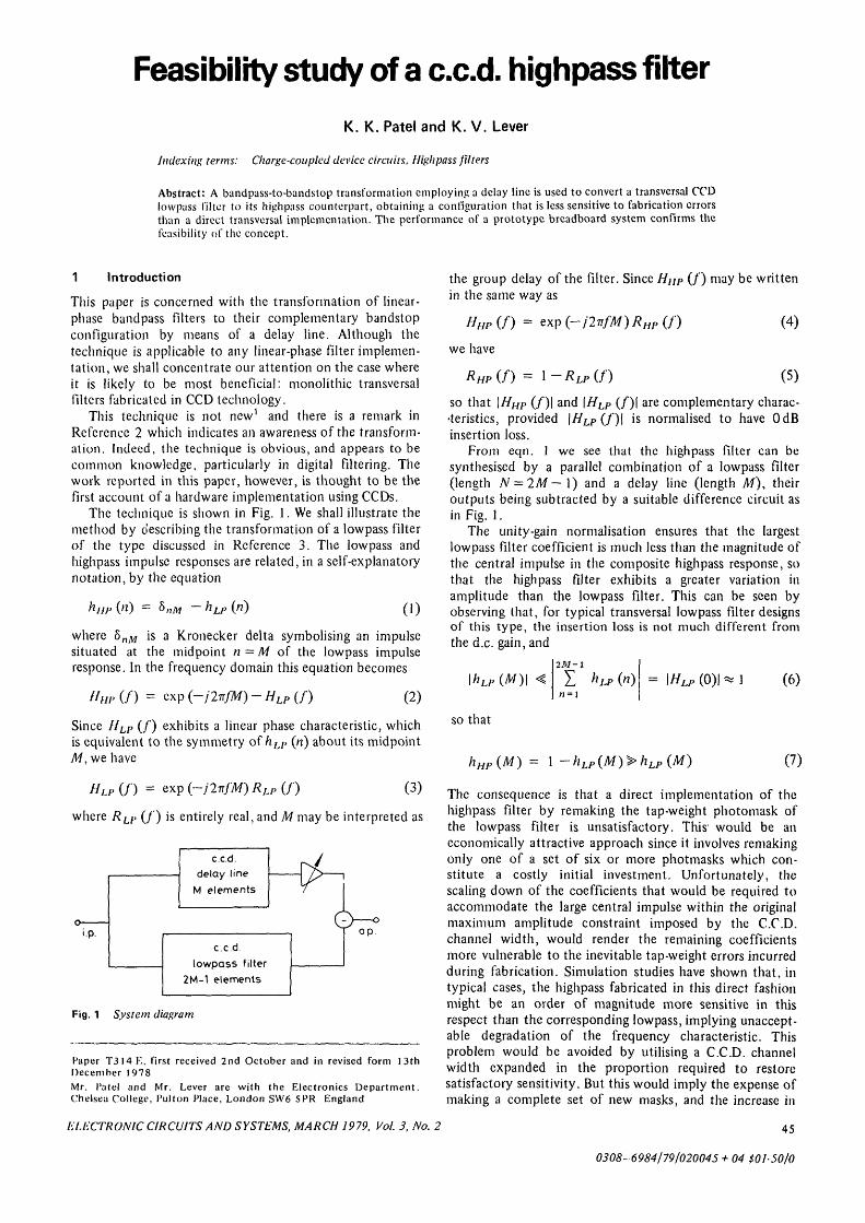
The technique is shown in Fig. 1. We shall illustrate themethod by describing the transformation of a lowpass filterof the type discussed in Reference 3. The lowpass andhighpass impulse responses are related, in a self-explanatorynotation, by the equation
hnP{n) = hnM -hLP{n) 0)where 5,,^ is a Kronecker delta symbolising an impulsesituated at the midpoint n—M of the lowpass impulseresponse. In the frequency domain this equation becomes
/ / „ , , ( / ) = exp ( - /27 r /M) - / / L P ( / ) (2)
Since IILP ( /) exhibits a linear phase characteristic, whichis equivalent to the symmetry ofhLP (n) about its midpointM, we have
HLp RLP
(3)
where RLP ( / ) is entirely real, and M may be interpreted as
p
c.c.d.delay line
M elements
c.c.d.lowpass filter
2M-1 elements
Fig. 1 System diagram
the group delay of the filter. Since Hl{P (/) may be writtenin the same way as
HHP{f) = exp(-/2nfM)RHP(f)
we have
(4)
(5)
so that \HHP ( / ) | and \HLP ( / ) | are complementary charac-•teristics, provided \HLP(f)\ is normalised to have OdBinsertion loss.
From eqn. 1 we see that the highpass filter can besynthesised by a parallel combination of a lowpass filter(length N = 2M— 1) and a delay line (length M), theiroutputs being subtracted by a suitable difference circuit asin Fig. 1.
The unity-gain normalisation ensures that the largestlowpass filter coefficient is much less than the magnitude ofthe central impulse in the composite highpass response, sothat the highpass filter exhibits a greater variation inamplitude than the lowpass filter. This can be seen byobserving that, for typical transversal lowpass filter designsof this type, the insertion loss is not much different fromthe d.c. gain, and
\hLP(M)\ <2M-1
LP (n) (0)1
so that
hHP{M) = 1 -hLP(M)>hLP(M)
(6)
(7)
Paper T314 P., first received 2nd October and in revised form 13thDecember 1978Mr. Pate! and Mr. Lever are with the Electronics Department.Chelsea College, Pulton Place, London SW6 5PR England
ELECTRONIC CIRCUITS AND SYSTEMS, MARCH 1979, Vol. 3, No. 2
The consequence is that a direct implementation of thehighpass filter by remaking the tap-weight photomask ofthe lowpass filter is unsatisfactory. This' would be aneconomically attractive approach since it involves remakingonly one of a set of six or more photmasks which con-stitute a costly initial investment. Unfortunately, thescaling down of the coefficients that would be required toaccommodate the large central impulse within the originalmaximum amplitude constraint imposed by the C.C.D.channel width, would render the remaining coefficientsmore vulnerable to the inevitable tap-weight errors incurredduring fabrication. Simulation studies have shown that, intypical cases, the highpass fabricated in this direct fashionmight be an order of magnitude more sensitive in thisrespect than the corresponding lowpass, implying unaccept-able degradation of the frequency characteristic. Thisproblem would be avoided by utilising a C.C.D. channelwidth expanded in the proportion required to restoresatisfactory sensitivity. But this would imply the expense ofmaking a complete set of new masks, and the increase in
45
0308-6984/79/020045 + 04 $01-50/0
chip size would lower the fabrication yield, implying anunacceptably high manufacturing cost.
The approach suggested in this paper leads to a satisfac-tory performance, in that the sensitivity of the lowpass-delay line configuration is basically that of the lowpass. Theperformance does depend on the accuracy of the differ-encing process, but this (unlike the fixed tap-weight errors)is amenable to accurate control: the sensitivity is concen-trated, as it were, in a single accessible parameter, therelative gain of the two parallel signal paths.
We have constructed a prototype breadboard systemusing state-of-the-art CCDs to test the validity of theseideas. We were not able to procure off-the-shelf delay linesand lowpass filters having the correct number of transversaldelay elements in the ratio M to 2M — 1. Accordingly, wesimulated the proposed system by using available devices:256-element delay lines (GEC CD256) and 100-elementlowpass filters (GEC MA344). In this configuration it isnecessary to clock the delay line and lowpass filter separ-ately, with the ratio of clock frequencies designed to ensurethat the total delay through the delay line is equal to thegroup delay of the lowpass filter. This arrangementnecessitates the use of separate sample-and-hold units toremove the clock components in the outputs from the twodevices.
2 Circuit design
The circuit is shown schematically in Fig. 2. A master clockof frequency fM is divided down by factors of 256 and 50using T.T.L. programmable counters, to provide thelowpass filter and delay line clocks, respectively. Theseratios provide a relationship between total delay of thedelay line and lowpass filter group delay close to thatrequired by the design.
Both the delay line and lowpass filter are operated in thethree-phase mode with fM chosen arbitrarily so that thelowpass filter bandwidth is 34kHz. In this configurationthe clocking frequencies are:fLPF = 64k H/,,fDL = 334kHzand/in - 16-38MHz.
The output of the delay line, which has an on-chip sensecircuit, is followed by an S/H unit to attenuate the fDL
i.p.
CD 256256-element delay line
and sense circuit
masterclock
divide by 50
divide by 256
W 5 0
fM/256
1 V2
3-phase clockgenerator
3-phase clockgenerator
fil
MA 344100-element lowpass filter
clock component. The lowpass filter requires external sensecircuitry; a suitable differential charge sensing amplifier canbe easily constructed from linear integrated circuits. Again,an output S/H unit is required to attenuate the clockcomponent at fLpF. The outputs from the delay line andlowpass filter S/H units are subtracted by means of adifferential amplifier. For this application a common moderejection ratio of 65 dB is adequate. The variable-gainamplifier \A\ determines the relative gains of the twoparallel signal paths. We found that it was necessary tocontrol the relative gain to better than 1% in order toobtain adequate cancellation in the highpass filter stopband.
3 Measured performance
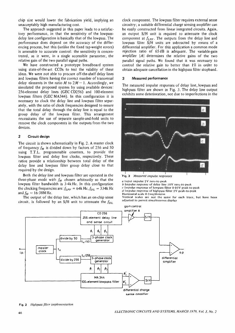
The measured impulse responses of delay line, lowpass andhighpass filter are shown in Fig. 3. The delay line outputexhibits some deterioration, not due to imperfections in the
Fig. 3 Measured impulse responses
a Input impulse 2V zero-to-peakb Impulse response of delay line 10V zero-to-peakc Impulse response of lowpass filter 003V peak-to-peakd Impulse response of highpass filter 2 V peak-to-peakHorizontal scale 0-2ms/divisionVertical scales are not the same for each trace, but haveadjusted to permit simultaneous display
gain controlamplifier A
been
S/H
differentialamplifier
differential chargesense nmnlifier
Fig. 2 Highpass filter implementation
46 ELECTRONIC CIRCUITS AND SYSTEMS, MARCH 1979, Vol. 3, No. 2
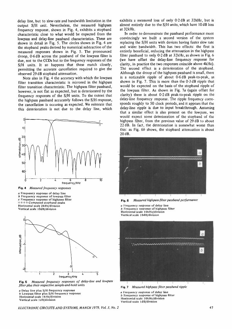
delay line, but to slew-rate and bandwidth limitation in theoutput S/H unit. Nevertheless, the measured highpassfrequency response, shown in Fig. 4, exhibits a stopbandcharacteristic close to what would be expected from thelowpass and delay-line passband characteristics. These areshown in detail in Fig. 5. The circles shown in Fig. 4 arethe stopband peaks derived by numerical subtraction of themeasured responses shown in Fig. 5. The pronounceddroop, 0-6 dB across the passband of the lowpass filter isdue, not to the CCDs but to the frequency responses of theS/H units. It so happens that these match closely,permitting the accurate cancellation required to give theobserved 29 dB stopband attenuation.
Note also in Fig. 4 the accuracy with which the lowpassfilter transition characteristic is mirrored in the highpassfilter transition characteristic. The highpass filter passband,however, is not flat as expected, but is deteriorated by thefrequency responses of the S/H units. To the extent thatthe highpass passband accurately follows the S/H response,the cancellation is occuring as expected. We reiterate thatthis deterioration is not due to the delay line, which
o 2
Fig. 4 Measured frequency responses
a Frequency response of delay lineb Frequency response of lowpass filterc Frequency response of highpass filtero o o o Computed stopband peaksHorizontal scale 2kHz/divisionVertical scale lbdB/division
6 8frequency, KHz
-2
frequency.KHz
Fig; 5 Measured frequency responses of delay-line and lowpassfilter plus their respective sample-and-hold units
a Delay line plus S/H frequency responseb Lowpass filter plus S/H frequency responseHorizontal scale lkHz/divisionVertical scale ldB/division
exhibits a measured loss of only 0-2 dB at 32kHz, but isalmost entirely due to the S/H units, which have lOdB lossat 32kHz.
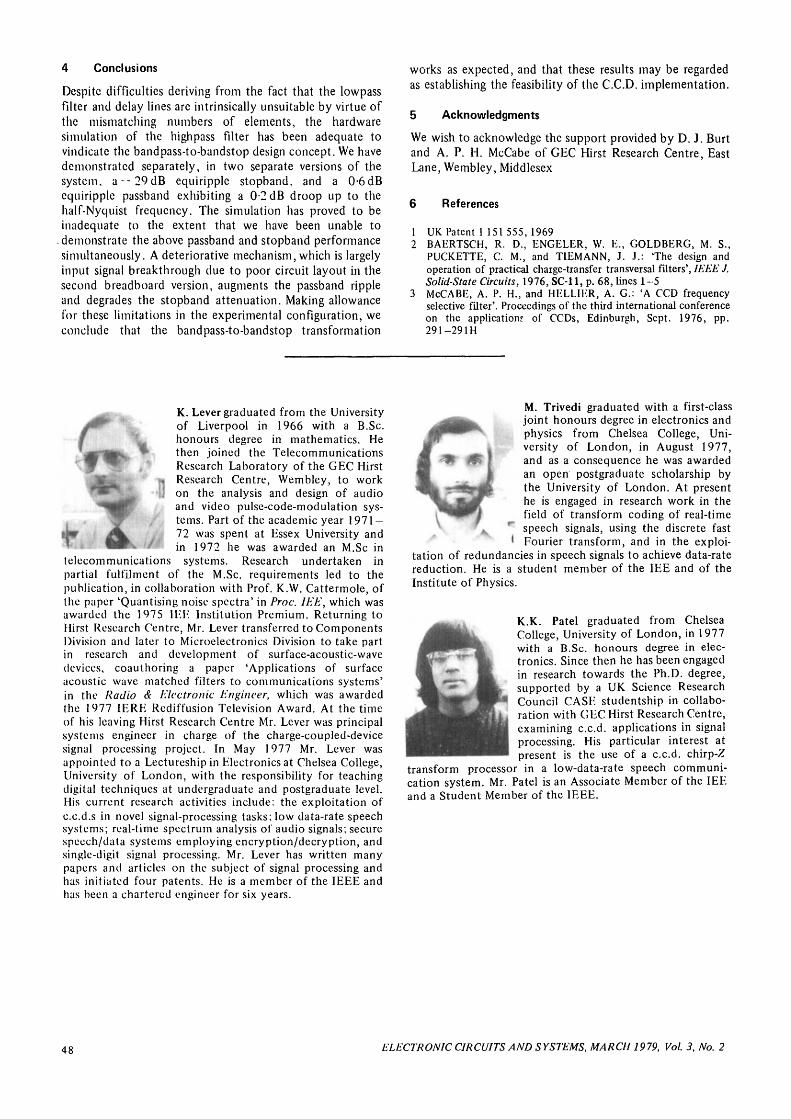
In order to demonstrate the passband performance moreconvincingly we built a second version of the systemreplacing the S/H units with devices having faster slew rateand wider bandwidth. This has two effects: the first isentirely beneficial, reducing the attenuation in the highpassfilter passband to only 0-2 dB at 32kHz, as shown in Fig. 6(we have offset the delay-line frequency response forclarity, in practice the two responses coincide above 4kHz).The second effect is a deterioration of the stopband.Although the droop of the highpass passband is small, thereis a noticeable ripple of about 0-6 dB peak-to-peak, asshown in Fig. 7. This is more than the 0-3 dB ripple thatwould be expected on the basis of the stopband ripple ofthe lowpass filter. As shown in Fig. la (again offset forclarity) there is about 0-2 dB peak-to-peak ripple on thedelay-line frequency response. The ripple frequency corre-sponds roughly to 50 clock periods, and it appears that thedelay-line ripple is due to input breakthrough. Assumingthat a similar effect is also present on the lowpass, wewould expect some deterioration of the stopband of thehighpass filter, from the previous value of 29 dB to about22 dB. In fact, the deterioration is somewhat worse thanthis: as Fig. 6b shows, the stopband attenuation is about20 dB.
Fig. 6 Measured highpass-filter passband performance
a Frequency response of delay lineb Frequency response of highpass filterHorizontal scale lOkHz/divisionVertical scale lOdB/division
Fig. 7 Measured highpass filter passband ripple
a Frequency response of delay lineb Frequency response of highpass filterHorizontal scale lOkHz/divisionVertical scale ldB/division
ELECTRONIC CIRCUITS AND SYSTEMS, MARCH 1979, Vol. 3, No. 2 47
4 Conclusions
Despite difficulties deriving from the fact that the lowpassfilter and delay lines are intrinsically unsuitable by virtue ofthe mismatching numbers of elements, the hardwaresimulation of the highpass filter has been adequate tovindicate the bandpass-to-bandstop design concept. We havedemonstrated separately, in two separate versions of thesystem, a--29dB equiripple stopband, and a 0-6dBequiripple passband exhibiting a 0-2 dB droop up to thehalf-Nyquist frequency. The simulation has proved to beinadequate to the extent that we have been unable todemonstrate the above passband and stopband performancesimultaneously. A deteriorative mechanism, which is largelyinput signal breakthrough due to poor circuit layout in thesecond breadboard version, augments the passband rippleand degrades the stopband attenuation. Making allowancefor these limitations in the experimental configuration, weconclude that the bandpass-to-bandstop transformation
works as expected, and that these results may be regardedas establishing the feasibility of the C.C.D. implementation.
5 Acknowledgments
We wish to acknowledge the support provided by D. J. Burtand A. P. H. McCabe of GEC Hirst Research Centre, EastLane, Wembley, Middlesex
6 References
1 UK Patent 1 151555,19692 BAERTSCH, R. D., ENGELER, W. E., GOLDBERG, M. S.,
PUCKETTE, C. M., and TIEMANN, J. J.: 'The design andoperation of practical charge-transfer transversal filters', IEEE J.Solid-State Circuits, 1976, SC-11, p. 68, lines 1-5
3 McCABE, A. P. H., and HELLIER, A. G.: 'A CCD frequencyselective filter'. Proceedings of the third international conferenceon the application? of CCDs, Edinburgh, Sept. 1976, pp.291-291H
K. Lever graduated from the Universityof Liverpool in 1966 with a B.Sc.honours degree in mathematics. Hethen joined the TelecommunicationsResearch Laboratory of the GEC HirstResearch Centre, Wembley, to workon the analysis and design of audioand video pulse-code-modulation sys-terns. Part of the academic year 1971 —^ w a s s P e n t a t Essex University and
telecommunications systems. Research undertaken inpartial fulfilment of the M.Sc. requirements led to thepublication, in collaboration with Prof. K.W. Cattermole, ofthe paper 'Quantising noise spectra' in Proc. IKK, which wasawarded the 1975 IEE Institution Premium. Returning toHirst Research Centre, Mr. Lever transferred to ComponentsDivision and later to Microelectronics Division to take partin research and development of surface-acoustic-wavedevices, coauthoring a paper 'Applications of surfaceacoustic wave matched filters to communications systems'in the Radio & Klectronic Kngincer, which was awardedthe 1977 IERE Rediffusion Television Award. At the timeof his leaving Hirst Research Centre Mr. Lever was principalsystems engineer in charge of the charge-coupled-devicesignal processing project. In May 1977 Mr. Lever wasappointed to a Lectureship in Electronics at Chelsea College,University of London, with the responsibility for teachingdigital techniques at undergraduate and postgraduate level.His current research activities include: the exploitation ofc.c.d.s in novel signal-processing tasks; low data-rate speechsystems; real-time spectrum analysis of audio signals; securespeech/data systems employing encryption/decryption, andsingle-digit signal processing. Mr. Lever has written manypapers and articles on the subject of signal processing andhas initiated four patents. He is a member of the IEEE andhas been a chartered engineer for six years.
M. Trivedi graduated with a first-classjoint honours degree in electronics andphysics from Chelsea College, Uni-versity of London, in August 1977,and as a consequence he was awardedan open postgraduate scholarship bythe University of London. At presenthe is engaged in research work in thefield of transform coding of real-time
*"" speech signals, using the discrete fasti Fourier transform, and in the exploi-
tation of redundancies in speech signals to achieve data-ratereduction. He is a student member of the IEE and of theInstitute of Physics.
K.K. Patel graduated from ChelseaCollege, University of London, in 1977with a B.Sc. honours degree in elec-tronics. Since then he has been engagedin research towards the Ph.D. degree,supported by a UK Science ResearchCouncil CASE studentship in collabo-ration with GEC Hirst Research Centre,examining c.c.d. applications in signalprocessing. His particular interest atpresent is the use of a c.c.d. chirp-Z
transform processor in a low-data-rate speech communi-cation system. Mr. Patel is an Associate Member of the IEEand a Student Member of the IEEE.
48 ELECTRONIC CIRCUITS AND SYSTEMS, MARCH 1979, Vol. 3, No. 2