Embed Size (px)
Citation preview

Application Note 83
AN83-1
Performance Verification of Low Noise,Low Dropout RegulatorsSilence of the Amps
Jim Williams and Todd Owen, Linear Technology Corporation
March 2000
Introduction
In an increasing trend, telecommunications, networking,audio and instrumentation require low noise power sup-plies. In particular, there is interest in low noise, lowdropout linear regulators (LDO). These components powernoise-sensitive circuitry, circuitry that contains noise-sensitive elements or both. Additionally, to conserve power,particularly in battery driven apparatus such as cellulartelephones, the regulators must operate with low input-to-output voltages.1 Devices presently becoming availablemeet these requirements (see separate section, “A Familyof 20µVRMS Noise, Low Dropout Regulators”).
Noise and Noise Testing
Establishing and specifying LDO dropout performance isrelatively easy to do. Verifying that a regulator meetsdropout specification is similarly straightforward. Accom-plishing the same missions for noise and noise testing isconsiderably more involved. The noise bandwidth of inter-est must be called out, along with operating conditions.Operating conditions can include regulator input andoutput voltage, load, assorted discrete components, etc.Low noise performance is effected by numerous subtle-ties; changes in operating conditions can cause unwel-come surprises.2 Because of this, LDO noise must bequoted under specified operating and bandwidth condi-tions to be meaningful. Failure to observe this precautionwill result in misleading data and erroneous conclusions.
Noise Testing Considerations
What noise bandwidth is of interest and why is it interest-ing? In most systems, the range of 10Hz to 100kHz is theinformation signal processing area of concern. Addition-ally, linear regulators produce little noise energy outsidethis region.3 These considerations suggest a measure- , LTC and LT are registered trademarks of Linear Technology Corporation.
Note 1: See Appendix A, “Architecture of a Low Noise LDO,” for designconsiderations of these devices.Note 2: See Appendix D, “Practical Considerations for Selecting a LowNoise LDO.”Note 3: Switching regulators are an entirely different proposition,requiring very broadband noise measurement. See Reference 1.Note 4: Component choice for the regulator, more critical than mightbe supposed, is discussed in Appendix B, “Capacitor SelectionConsiderations.”Note 5: The choice of RMS voltmeter is absolutely crucial to obtainmeaningful measurements. See Appendix C, “Understanding andSelecting RMS Voltmeters.”
ment bandpass of 10Hz to 100kHz, with steep slopes at theband limits. Figure 1 shows a conceptual filter for LDOnoise testing. The Butterworth sections are the key tosteep slopes and flatness in the passband. The small inputlevel requires 60dB of low noise gain to provide adequatesignal for the Butterworth filters. Figure 2 details the filterscheme. The regulator under test is at the diagram’scenter.4 A1-A3 make up a 60dB gain highpass section. A1and A2, extremely low noise devices (<1nV√Hz), comprisea 60dB gain stage with a 5Hz highpass input. A3 providesa 10Hz, 2nd order Butterworth highpass characteristic.The LTC®1562 filter block is arranged as a 4th orderButterworth lowpass. Its output is delivered via the330µF-100Ω highpass network. The circuit’s output drivesa thermally responding RMS voltmeter.5 Note that allcircuit power is furnished by batteries, precluding groundloops from corrupting the measurement.
Instrumentation Performance Verification
Good measurement technique dictates verifying the noisetest instrumentation’s performance. Figure 3’s spectralplot of the filter section shows essentially flat response inthe 10Hz to 100kHz passband with abrupt slopes at theband extremes. Figure 4, expanding the vertical scale to

Application Note 83
AN83-2
A FAMILY OF 20µVRMS NOISE, LOW DROPOUTREGULATORS
Telecom and instrumentation applications often requirea low noise voltage regulator. Frequently this require-ment coincides with the need for low regulator dropoutand small quiescent current. A recently introduced familyof devices addresses this problem. Figure A shows avariety of packages, power ranges and features in threebasic regulator types. The SOT-23 packaged LT®1761has only 20µVRMS noise with 300mV dropout at 100mA.Quiescent current is only 20µA.
Applying the Regulators
Applying the regulators is simple. Figure B shows aminimum parts count, 3.3V output design. This circuitappears similar to conventional approaches with a no-table exception: a bypass pin (BYP) is returned to theoutput via a 0.01µF capacitor. This path filters the internalreference’s output, minimizing regulator output noise. Itis the key to the 20µVRMS noise performance. A shut-down pin (SHDN), when pulled low, turns off the regula-tor output while keeping current drain inside 1µA. Dropoutcharacteristics appear in Figure C. Dropout scales withoutput current, falling to less than 100mV at low cur-rents.
These devices provide the lowest available output noisein a low dropout regulator without compromising otherparameters. Their performance, ease of use and versatil-ity allow use in a variety of noise-sensitive applications.
1µF
10µF
AN83 FigB
3.3V/100mA20µVRMSNOISE (TYP)
VIN > 3.7V
0.01µF
SHDN
IN
GND
LT1761-3.3
OUT
BYP
+
TEMPERATURE (°C)–50
DROP
OUT
VOLT
AGE
(mV)
0 50 75
AN83 FigC
–25 25 100 125
IL = 100mA
IL = 50mA
IL = 10mA
IL = 1mA
500
450
400
350
300
250
200
150
100
50
0
Figure B. Applying the Low Noise, Low Dropout,Micropower Regulator. Bypass Pin and AssociatedCapacitor are Key to Low Noise Performance Figure C. Figure B’s Dropout Voltage at Various Currents
RMS NOISEREGULATOR OUTPUT (10Hz to 100kHz) PACKAGE QUIESCENT SHUTDOWNTYPE CURRENT CBYP = 0.01µF OPTIONS FEATURES CURRENT CURRENT
LT1761 100mA 20µVRMS SOT23-5 Shutdown, Reference Bypass, Adjustable Output; 20µA <1µASOT23 Package Mandates Selecting Any Two Features
LT1762 150mA 20µVRMS MSOP-8 Shutdown, Reference Bypass, Adjustable Output 25µA <1µA
LT1962 300mA 20µVRMS MSOP-8 Shutdown, Reference Bypass, Adjustable Output 30µA <1µA
LT1763 500mA 20µVRMS SO-8 Shutdown, Reference Bypass, Adjustable Output 30µA <1µA
LT1963 1.5A 40µVRMS SO-8, SOT223-3, Shutdown, Adjustable Output, Fast Transient Response 1mA <1µADD-5, TO220
LT1764 3A 40µVRMS DD-5, TO220 Shutdown, Adjustable Output, Fast Transient Response 1mA <1µA
Figure A. Low Noise LDO Family Short-Form Specifications. Quiescent Current Scaleswith Output Current Capability, Although Noise Performance Remains Nearly Constant

Application Note 83
AN83-3
1dB/division, reveals some flatness deviation but wellwithin 1dB throughout nearly the entire passband. Ground-ing the filter’s input determines the tester’s noise floor.Figure 5 shows less than 4µVP-P, corresponding to a0.5µVRMS voltmeter reading. This is only about 0.5% offull scale (100µVRMS), contributing negligible error. Theseresults assure the confidence necessary to proceed withregulator noise measurement.
Regulator Noise Measurement
Regulator noise measurement begins with attention totest setup details. The extremely low signal levels requireattention to shielding, cable management, layout andcomponent choice.6 Figure 6a is the bench arrangement.The photo shows the completely shielded environmentrequired to obtain faithful noise measurements. The metalcan7 encloses the regulator under test and its internalbattery power supply. A BNC fitting (photo lower center)connects the regulator output to the noise filter test circuit(black box). Note that the monitoring oscilloscope andvoltmeter are not simultaneously connected to the output,precluding ground loops which would corrupt themeasurement.
Figure 6b details the regulator enclosure with its coverremoved. The battery supply is visible; the regulatoroccupies the can center. The BNC fitting connecting thenoise filter box (lower left) eliminates triboelectric distur-bances a cable might contribute.
Figure 6c is the noise test circuit box. Functions are aslabeled in the photo. The two capped BNC connectors (boxlower) are unused box entries.
Note 6: Capacitor choice is discussed in Appendix B, “CapacitorSelection Considerations.”Note 7: The cookies were excellent, particularly the thin ones withsugar on top.Note 8: See Appendix A, “Architecture of a Low Noise LDO,” fordetails.
Figure 7’s oscilloscope photo shows an LT1761 regulator’snoise measured at the filter output. Monitoring this pointwith the RMS voltmeter shows a 20µVRMS reading.Figure 8’s spectral plot of this noise indicates diminishedpower above 1kHz, in accordance with expected regulatornoise density. Figure 9 shows more complete spectralnoise density data for three regulator types. Noise powerdecays uniformly with increasing frequency, although thethree regulators show some dispersion below 200Hz.
Bypass Capacitor (CBYP) Influence
The regulator’s internal voltage reference contributes mostof the device’s noise. The reference bypass capacitorfilters reference noise, precluding it from appearing, inamplified form, at the output.8 Figure 10 is a study ofregulator noise vs various values of CBYP. 10a showssubstantial noise for CBYP = 0µF, while 10d displays nearly9× improvement with CBYP = 0.01µF; intermediate valuesof CBYP (10b and 10c) produce commensurateresults.
Interpreting Comparative Results
Figure 11’s photos compare an LT1761-5’s output noise(11d) with three other regulators (11a, 11b and 11c).These three devices are manufacturer specified for lownoise performance, but the photos do not indicate this.The seeming contradication is probably due to ambiguityin testing methods or specifications. For example, inap-propriate choice of test equipment (see Appendix C) ormeasurement bandwidth can easily cause huge (5×)errors. This uncertainty mandates the noise testing de-scribed to insure realistic conclusions.

Application Note 83
AN83-4
10µFRLOAD(TYPICALLY100mA)
TYPICAL REGULATOR UNDER TEST
5VOUT
EXTERNAL INPUT
–
+A1
LT1028100Ω330µF
INPUT
3.16k
+
ALL RESISTORS 1% METAL FILM4.7µF CAPACITORS = MYLAR, WIMA MKS-2330µF CAPACITORS = SANYO OSCON±4.5V DERIVED FROM 6AA CELLSPOWER REGULATOR FROM APPROPRIATE NUMBER OF D SIZE BATTERIES
+
–
+A2
LT1028100Ω
6.19k 2k
5.9K
–
+A3
LT1224
2.49k
4.99k
4.7µF 4.5V
–4.5V
4.7µF
NORMALINPUT
1µF
VIN
IN OUT
SHDN BYPGND
LT1761-5 0.01µF
100Ω
OUTPUT TO THERMALLY RESPONDINGRMS VOLTMETER0.1V FULL SCALE = 100µVRMS NOISE10Hz TO 100kHz BW
AN83 F02
330µF
+
LTC1562
10k
5.62k
1 20
2 19
3 18
4 17
5 16
6 15
7 14
8 13
9 12
10 11
10k
–4.5V–4.5V
4.5V
13k
17.8k
110k
43.2k
110k
10k
110k
110k
10k
Figure 2. Implementation of Figure 1. Low Noise Amplifiers Provide Gain and InitialHighpass Shaping. LTC1562 Filter Supplies 4th Order Butterworth Lowpass Characteristic
5Hz SINGLE ORDERHIGHPASS
IN 10Hz TO 100kHz
AN83 F01
GAIN = 60dB
10Hz 2nd ORDERBUTTERWORTH HP
100kHz 4th ORDERBUTTERWORTH LP
5Hz SINGLE ORDERHIGHPASS
Figure 1. Filter Structure for Noise Testing LDOs. ButterworthSections Provide Appropriate Response in Desired Frequency Range

Application Note 83
AN83-5
Figure 3. HP-4195A Spectrum Analyzer Plot ofFilter Characteristics. Filter Performance IsNearly Flat Over Desired 10Hz to 100kHz Rangewith Steep Rolloff Outside Bandpass Region
Figure 4. Expanded Scale Examination of Passband ShowsFlatness within 1dB Over Almost Entire Measurement Range
Figure 5. <4µVP-P Test Setup Noise Residue Correspondsto About 0.5µVRMS Measurement Noise Floor
1ms/DIV AN83 F05
2µV/DIV
AN83 F04.epsAN83 F03.eps

Application Note 83
AN83-6
Figure 6a. LDO Noise Measurement Bench Setup. Shielded Can Contains Regulator; NoiseFilter Circuitry Occupies Box at Photo Lower Center. Oscilloscope and RMS Voltmeter AreNot Simultaneously Connected, Precluding Ground Loop from Corrupting Measurement
AN83 F06a
Figure 6b. Shielded can with Cover Removed. LDO Under Test Occupies Center. D-CellsProvide Power, Eliminate Potential Ground Loop. BNC Fitting (Photo Lower Left) ConnectsOutput to Filter Circuit Test Box, Minimizing Triboelectric Based Errors
AN83 F06b

Application Note 83
AN83-7
Figure 6c. Noise Filter Test Box Is Fully Shielded. Connections Are As Indicated.Capped BNC Fittings (Photo Low Center and Right) Are Unused Entries
AN83 F06b
Figure 7. LT1761 Output Voltage Noise in a 10Hz to100kHz Bandwidth. RMS Noise Measures 20µVRMS
1ms/DIV AN83 F07
ENOISE100µV/DIV
FREQUENCY (Hz)10k
AN 83 F09
10
1
0.1
0.0110 100 1k 100k
OUTP
UT V
OLTA
GE N
OISE
(µV/
√Hz)
LT1761
LT1761-3.3
LT1761-5
Figure 8. Noise Spectrum Plot ShowsDiminishing Power Above 1kHz
AN83 F08.eps
Figure 9. Output Noise Spectral Density Data Curvesfor Three Regulators Show Dispersion Below 200Hz
CBYP = 1000pF

Application Note 83
AN83-8
(10a) LT1761-510Hz to 100kHz Output NoiseCBYP = 0
COUT = 10µF 1ms/DIV AN83 F10a.tif
IL = 100mA
VOUT100µV/DIV
(10b) LT1761-510Hz to 100kHz Output NoiseCBYP = 100pF
COUT = 10µF 1ms/DIV AN83 F10b.tif
IL = 100mA
VOUT100µV/DIV
(10c) LT1761-510Hz to 100kHz Output NoiseCBYP = 1000pF
COUT = 10µF 1ms/DIV AN83 F10c.tif
IL = 100mA
VOUT100µV/DIV
(10d) LT1761-510Hz to 100kHz Output NoiseCBYP = 0.01µF
COUT = 10µF 1ms/DIV AN83 F10d.tif
IL = 100mA
VOUT100µV/DIV
Figure 10. Regulator Noise for Various Bypass Capacitor(CBYP) Values. Noise Decreases with Increasing CBYP

Application Note 83
AN83-9
(11a) Manufacturer “MI” Output Voltage Noise (5V Output)
1ms/DIV AN83 F11a.tif
ENOISE100µV/DIV
(11b) Manufacturer “NS” Output Voltage Noise (5V Output)
1ms/DIV AN83 F11b.tif
ENOISE100µV/DIV
(11c) Manufacturer “MA” Output Voltage Noise (5V Output)
1ms/DIV AN83 F11c.tif
ENOISE100µV/DIV
(11d) LT1761-5 Output Voltage Noise (5V Output)
1ms/DIV AN83 F11d.tif
Figure 11. Noise for LT1761-5 vs Three Other Devices.“C” Is Specified for RMS Noise Figure Approaching the LT1761-5,but in a Restricted Noise Measurement Bandwidth. Caveat Emptor!
ENOISE100µV/DIV
Application Note 83
AN83-10
REFERENCES
1. Williams, J., “A Monolithic Switching Regulator with100µV Output Noise,” Linear Technology Corpora-tion, Application Note 70, October 1997.
2. Sheingold, D. H. (editor), “Nonlinear Circuits Hand-book,” 2nd Edition, Analog Devices, Inc., 1976.
3. Kitchen, C., Counts, L., “RMS-to-DC ConversionGuide,” Analog Devices, Inc. 1986.
4. Williams, J., “Practical Circuitry for Measurement andControl Problems,” “Broadband Random Noise Gen-erator,” “Symmetrical White Gaussian Noise” Appen-dix B, Linear Technology Corporation, ApplicationNote 61, August 1994, pp. 24–26, pp. 38–39.
5. General Radio Company, Type 1390B Random NoiseGenerator Operating Instructions, October 1961.
6. Hewlett-Packard Company, “1968 Instrumentation.Electronic—Analytical—Medical,” AC Voltage Mea-surement, Hewlett-Packard Company, 1968, pp. 197–198.
7. Justice, G., “An RMS-Responding Voltmeter withHigh Crest Factor Rating,” Hewlett-Packard Journal,Hewlett-Packard Company, January 1964.
8. Hewlett-Packard Company, “Model HP3400A RMSVoltmeter Operating and Service Manual,” Hewlett-Packard Company, 1965.
9. Williams, J., “A Monolithic IC for 100MHz RMS/DCConversion,” Linear Technology Corporation, Appli-cation Note 22, September 1987.
10. Ott, W.E., “A New Technique of Thermal RMS Mea-surement,” IEEE Journal of Solid State Circuits, De-cember 1974.
11. Williams, J.M. and Longman, T.L., “ A 25MHz Ther-mally Based RMS-DC Converter,” 1986 IEEE ISSCCDigest of Technical Papers.
12. O’Neill, P.M., “ A Monolithic Thermal Converter,” H.P.Journal, May 1980.
13. Williams, J., “A Fourth Generation of LCD BacklightTechnology,” “RMS Voltmeters,” Linear TechnologyCorporation, Application Note 65, November 1995,pp. 82–83.
14. Tektronix, Inc., “Type 1A7A Differential Amplifier In-struction Manual,” Check Overall Noise Level Tangen-tially, 1968, pp. 5-36 and 5-37.
Note: This application note was derived from a manuscript originally prepared for publication in EDNmagazine.
Application Note 83
AN83-11
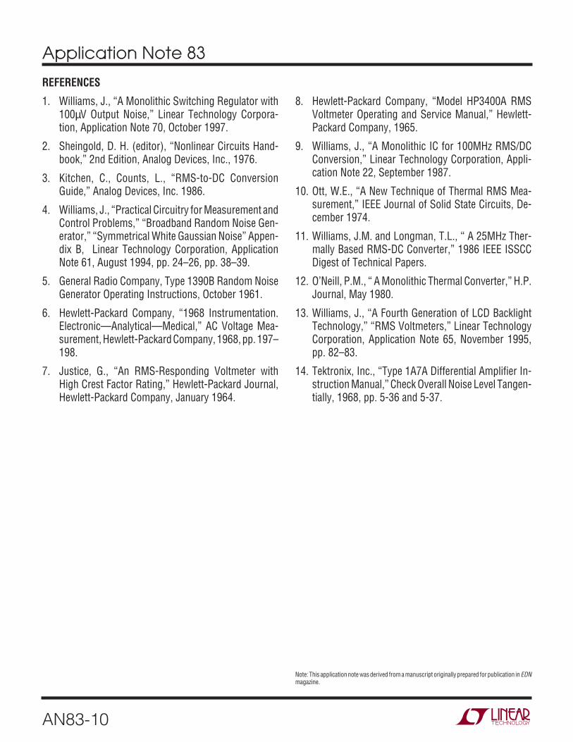
APPENDIX A
ARCHITECTURE OF A LOW NOISE LDO
Noise Minimization
The low noise LDOs use Figure A1’s scheme, with specialattention to minimizing noise transmission within the loopand from unregulated input. The internal voltage reference’snoise is filtered by CBYP. Additionally, the error amplifier’sfrequency response is shaped to minimize noise contribu-tion while preserving transient response and PSRR. Regu-lators which do not do this have poor noise rejection andtransient performance.
Pass Element Considerations
Extremely low dropout voltage requires considering thepass element. Dropout limitations are set by the passelements on-impedance limits. The ideal pass element haszero impedance capability between input and output andconsumes no drive energy.
A number of design and technology options offer varioustrade-offs and advantages. Figure A2 lists some passelement candidates. Followers offer current gain, ease ofloop compensation (voltage gain is below unity) and thedrive current ends up going to the load. Unfortunately,saturating a follower requires voltage overdriving theinput (e.g. base, gate). Since drive is usually deriveddirectly from VIN, this is difficult. Practical circuits musteither generate the overdrive or obtain it elsewhere. With-out voltage overdrive, the saturation loss is set by VBE inthe bipolar case and channel on-resistance for MOS. MOSchannel on-resistance varies considerably under theseconditions, although bipolar losses are more predictable.Note that voltage losses in driver stages (Darlington, etc.)add directly to the dropout voltage. The follower outputused in conventional 3-terminal IC regulators combineswith drive stage losses to set dropout at 3V.
Common emitter/source is another pass element option.This configuration removes the VBE loss in the bipolarcase. The PNP version is easily fully saturated, even in ICform. The trade-off is that the base current never arrives atthe load, wasting power. At higher currents, base drivelosses can negate a common emitter’s saturation advan-tage. As in the follower example, Darlington connectionsexacerbate the problem. Achieving low dropout in a mono-lithic PNP regulator requires a PNP structure that attainslow dropout while minimizing base drive loss. This isparticularly the case at higher pass currents. Considerableeffort was expended in this direction in the LT176X throughLT196X designs.
Common source connected P-channel MOSFETs are alsocandidates. The do not suffer the drive losses of bipolars,but typically require volts of gate-channel bias to fullysaturate. In low voltage applications this may requiregeneration of negative potentials. Additionally, P-channeldevices have poorer saturation than equivalent sizeN-channel devices.
The voltage gain of common emitter and source configu-rations is a loop stability concern but is manageable.
Compound connections using a PNP driven NPN are areasonable compromise, particularly for high power (be-yond 250mA) IC construction. The trade-off between thePNP VCE saturation term and reduced drive losses over aconventional PNP structure is favorable. Also, the majorcurrent flow is through a power NPN, easily realized inmonolithic form. The connection has voltage gain, neces-sitating attention to loop frequency compensation. Regu-lators utilizing this pass scheme can supply up to 7.5A withdropouts below 1.5V (LT1083 through LT1086 series).
Readers are invited to submit results obtained with ouremeritus thermionic friends, shown out of respectfulcourtesy.

Application Note 83
AN83-12
Dynamic Characteristics
The LT176X through LT196X’s low quiescent currents donot preclude good dynamics. Usually, low quiescent powerdevices are associated with slow dynamics and instability.The devices are stable (no output oscillation) even withlow ESR ceramic output capacitors. This contrasts withconventional LDO regulators that often oscillate with ce-ramic capacitors.
PASSELEMENT
VREF
INPUT OUTPUT
ERRORAMPLIFIER
REGULATINGLOOP
CBYP
AN83 FA01
VIN VOUT
AN83 FA02
VIN VOUT
VIN VOUT
VIN VOUT VOUT
VIN VOUT
VIN
–V
VOUT
VIN
FOLLOWERSCOMMON
EMITTER/SOURCE COMPOUND
Figure A3. Transient Response without Noise Bypass Capacitor
200µs/DIV AN83 FA03.tif
VOUT100mV/DIV
Figure A1. Simplified Low Noise LDO Regulator.Voltage Reference Is Filtered by CBYP, IsolatingNoise from Regulating Loop. Error Amplifier’sFrequency Compensation Prevents Transmission ofInput Noise While Preserving Transient Response
Figure A2. Linear Regulator Pass Element Candidates
The internal architecture provides an added bonus intransient performance when the 0.01µF noise capacitor isadded. Transient response for a 10mA to 100mA load stepwith a 10µF output capacitor appears in Figure A3 with thecapacitor deleted. Figure A4 shows the same situationwith the 0.01µF bypass capacitor in place. Settling timeand amplitude are markedly reduced.
Figure A4. Noise Bypass Capacitor ImprovesTransient Response. Note Voltage Scale Change
200µs/DIV AN83 FA04.tif
VOUT20mV/DIV

Application Note 83
AN83-13
APPENDIX B
CAPACITOR SELECTION CONSIDERATIONS
Bypass Capacitance and Low Noise Performance
Adding a capacitor from the regulators VOUT to BYP pinlowers output noise. A good quality low leakage capacitoris recommended. This capacitor bypasses the regulator’sreference, providing a low frequency noise pole. A 0.01µFcapacitor lowers the output voltage noise to 20µVRMS.Using a bypass capacitor also improves transient re-sponse. With no bypassing and a 10µF output capacitor,a 10mA to 500mA load step settles within 1% of final valuein under 100µs. With a 0.01µF bypass capacitor, theoutput settles within 1% for the same load step in under10µs; total output deviation is inside 2.5%. Regulatorstart-up time is inversely proportional to bypass capacitorsize, slowing to 15ms with a 0.01µF bypass capacitor and10µF at the output.
Output Capacitance and Transient Response
The regulators are designed to be stable with a wide rangeof output capacitors. Output capacitor ESR affects stabil-ity, most notably with small capacitors. A 3.3µF minimumoutput value with ESR of 3Ω or less is recommended toprevent oscillation. Transient response is a function ofoutput capacitance. Larger values of output capacitancedecrease peak deviations, providing improved transientresponse for large load current changes. Bypass capaci-tors, used to decouple individual components powered by
the regulator, increase effective output capacitor value.Larger values of reference bypass capacitance dictatelarger output capacitors. For 100pF of bypass capaci-tance, 4.7µF of output capacitor is recommended. With1000pF of bypass capacitor or larger, a 6.8µF outputcapacitor is required.
Figure B1’s shaded region defines the regulator’s stabilityrange. Minimum ESR needed is set by the amount ofbypass capacitance used, while maximum ESR is 3Ω.
Ceramic Capacitors
Ceramic capacitors require extra consideration. They aremanufactured with a variety of dielectrics, each withdifferent behavior across temperature and applied volt-age. The most common dielectrics are Z5U, Y5V, X5R andX7R. The Z5U and Y5V dielectrics provide high capaci-tance in a small package, but exhibit strong voltage andtemperature coefficients as shown in Figures B2 and B3.Used with a 5V regulator, a 10µF Y5V capacitor showsvalue as low as 1µF to 2µF over the operating temperaturerange. The X5R and X7R dielectrics have more stablecharacteristics and are more suitable for output capacitoruse. The X7R type has better stability over temperature,while the X5R is less expensive and available in highervalues.
OUTPUT CAPACITANCE (µF)1
OUTP
UT C
APAC
ITOR
ESR
(Ω)
4.0
3.5
3.0
2.5
2.0
1.5
1.0
0.5
03 10
AN83 FB01
2 4 5 6 7 8 9
STABLE REGION
CBYP = 330pFCBYP = 100pF
CBYP = 0
CBYP > 3300pF
DC BIAS VOLTAGE (V)
CHAN
GE IN
VAL
UE (%
)
AN83 FB02
20
0
–20
–40
–60
–80
–1000 4 8 102 6 12 14
X5R
Y5V
16
BOTH CAPACITORS ARE 16V,1210 CASE SIZE, 10µF
Figure B1. Regulator Stability for Various Outputand Bypass (CBYP) Capacitor Characteristics
Figure B2. Ceramic Capacitor DC Bias CharacteristicsIndicate Pronounced Voltage Dependence. Device MustProvide Desired Capacitance Value at Operating Voltage

Application Note 83
AN83-14
APPENDIX C
UNDERSTANDING AND SELECTING RMSVOLTMETERS
The choice of AC voltmeter is absolutely crucial for mean-ingful measurements. The AC voltmeter must respondfaithfully to the RMS value of the measured noise. Themajority of AC voltmeters (including DVMs with AC ranges)are not capable of doing this. This includes instrumentswith “true RMS” AC scales. As such, selecting an appro-priate instrument requires care. The selection processbegins with a basic understanding of AC voltmeter types.1
AC Voltmeter Types
There are three basic AC voltmeter types. They includerectify and average, analog computing and thermal. Thethermal approach is the only one that is inherently accu-rate, regardless of input waveshape. This feature is par-ticularly relevant to noise RMS amplitude determination.
Rectify and Average
The rectify and average scheme (Figure C1) applies the ACinput to a precision rectifier. The rectifier output feeds asimple RC averager which is gain scaled, providing theoutput. In practice, gain is set so the DC output equals theRMS value of a sine wave input. If the input remains a puresine wave, accuracy can be quite good. However, nonsi-nosoidal inputs cause large errors. This type voltmeter isonly accurate for sine wave inputs, with increasing error asthe input departs from sinosoidal.
Voltage and temperature coefficients are not the onlyproblem sources. Some ceramic capacitors have a piezo-electric response. A piezoelectric device generates voltageacross its terminals due to mechanical stress, similar tothe way a piezoelectric accelerometer or microphoneworks. For a ceramic capacitor the stress can be inducedby vibrations in the system or thermal transients. The
resulting voltages produced can cause appreciable amountsof noise, especially when a ceramic capacitor is used fornoise bypassing. A ceramic capacitor produced Figure B4’strace in response to light tapping from a pencil. Similarvibration induced behavior can masquerade as increasedoutput voltage noise.
TEMPERATURE (°C)–50
40
20
0
–20
–40
–60
–80
–10025 75
AN83 FB03
–25 0 50 100 125
Y5V
CHAN
GE IN
VAL
UE (%
) X5R
BOTH CAPACITORS ARE 16V,1210 CASE SIZE, 10µF
Figure B4. A Ceramic Capacitor Responds to Light PencilTapping. Piezoelectric Based Response Approaches 80µVP-P
Figure B3. Ceramic Capacitor Temperture CharacteristicsShow Large Capacitance Shift. Effect Should Be ConsideredWhen Determining Circuit Error Budget
200ms/DIV AN83 FB04.tif
20µV/DIV
Note 1: Another way to approximately measure RMS AC noise usingan oscilloscope is the tangential method. See Reference 14.

Application Note 83
AN83-15
Note 2: See the References section for publications covering thermalAC–DC conversion.Note 3: Noise generators are worthy of study and considered inReferences 4 and 5.
Analog Computation
Figure C2 shows a more sophisticated AC voltmetermethod. Here, the instantaneous value is (ideally) continu-ously computed by an analog computational loop. The DCoutput follows the equation noted, resulting in muchbetter accuracy as input waveshape varies. Almost allcommercial implementations of this approach utilize loga-rithmically based analog computing techniques. Unfortu-nately, dynamic limitations in the ZY/X block dictatebandwidth restrictions. These circuits typically developsignificant errors beyond 20kHz to 200kHz.
Thermal
The thermally based AC voltmeter is inherently insensitiveto input waveshape, particularly suiting it to noise RMSamplitude measurement. Additionally, high accuracy atbandwidths exceeding 100MHz is achievable. Figure C3diagrams the classic thermal scheme.2 It is composed ofmatched heater-temperature sensor pairs and an ampli-fier. The AC input drives a heater, warming it. The tempera-ture sensor associated with this heater responds, biasing
the amplifier. The amplifier closes its feedback loop bydriving the output heater to warm its associated tempera-ture sensor. When the loop closes, the heaters are at thesame temperature. This “force-balance” action results inthe DC output equalling the input heater’s RMS heatingvalue—the fundamental definition of RMS. Changes inwaveshape have no effect, as they are effectively down-converted to heat. This “first principles” nature of opera-tion makes thermally based AC voltmeters ideal forquantitative RMS noise measurement.
Performance Comparison of Noise Driven ACVoltmeters
The wide performance variation of the above methods,and even within a method, mandates caution in selectingan AC voltmeter. Comparing AC voltmeters intended foruse in RMS noise measurements is illuminating. Figure C4shows a simple evaluation arrangement. The noise gen-erator drives the external input of text Figure 2, producinga suitably band passed input at the voltmeter under test.3
Z R
CY X
VIN2
VOUT
ZY
X
AVERAGE (AC INPUT2)DC OUTPUT =
= RMS OF AC INPUT+
–
AC INPUT
FIGURE DERIVED FROM REFERENCES 2 AND 3 AN83 FC02
Figure C2. Analog Computer Based AC-DC Converter. Loop Continuously ComputesInput’s RMS Value. Bandwidth Limitations Produce High Frequency Errors
AVERAGERAN83 FC01
PRECISIONFULL-WAVERECTIFIER
DC OUTPUTCALIBRATED TO RMS OF AC INPUTSINE WAVE
AC INPUT
Figure C1. Rectify-and-Average Based AC-DC Converter. Gain Is Set So DCOutput Equals RMS Value of Sine Wave Input. Nonsine Inputs Produce Errors

Application Note 83
AN83-16
Figure C5 shows results for 20 voltmeters. Four of thevoltmeters are thermal types; the remainder utilize loga-rithmic analog computing or rectify and average AC-DCconversion. The four thermal types agreed well within 1%.In fact, three of the thermal types were within 0.2%, whilethe fourth (HP3400A), a metered instrument, is onlyreadable to 1%. The other 16 voltmeters showed errors upto 48% relative to the thermal group! Note that the errorscause lower readings than are actually warranted; a poorlychosen voltmeter will give unfairly optimistic readings.
The lesson here is clear. It is essential to verify ACvoltmeter accuracy before proceeding with RMS noisemeasurement. Failure to do so may cause highly mislead-ing “results.”
Thermal Voltmeter Circuit
It is sometimes desirable to construct, rather than pur-chase, a thermal voltmeter. Figure C6’s circuit is appli-cable to noise measurement. Text Figure 2’s filter feedsA1. A1’s output biases A2, which provides additional ACgain. The LT1088 based RMS/DC converter is made up ofmatched pairs of heaters and diodes and a control ampli-fier. The LT1206 drives R1, producing heat which lowersD1’s voltage. Differentially connected A3 responds bydriving R2, via Q3, to heat D2, closing a loop around the
amplifier. Because the diodes and heater resistors arematched, A3’s DC output is related to the RMS value of theinput, regardless of input frequency or waveshape. Inpractice, residual LT1088 mismatches necessitate a gaintrim, which is implemented at A4. A4’s output is the circuitoutput.
Start-up or input overdrive can cause A2 to deliver exces-sive current to the LT1088 with resultant damage. C1 andC2 prevent this. Overdrive forces D1’s voltage to anabnormally low potential. C1 triggers low under theseconditions, pulling C2’s negative input low. This causesC2’s output to go high, putting A2 into shutdown andterminating the overload. After a time determined by theRC at C2’s input, A2 will be enabled. If the overloadcondition still exists, the loop will almost immediately shutA2 down again. This oscillatory action will continue,protecting the LT1088 until the overload condition isremoved.
To trim this circuit, connect its input to a 10mVRMS,100kHz signal. Set the 500Ω adjustment for exactly 100mVDC out. Next, apply a 100kHz, 100mVRMS input and trimthe 10k potentiometer for 1V DC out. Repeat this sequenceuntil the adjustments do not interact. Two passes shouldbe sufficient.
TEMPERATURESENSOR
DC OUTPUT = RMS OF INPUT
TEMPERATURESENSOR
THERMALINSULATION
AC INPUT
HEATER HEATER
AN83 FC03
DCAMPLIFIER
Figure C3. Thermally Based AC-DC Converter Converts AC Input to Heat. RemainingCircuitry Determines DC Value (Output) Required to Produce Identical Heating.Error Is Extraordinarily Low, Even at Waveshape and Bandwidth Extremes

Application Note 83
AN83-17
GENERAL RADIO1390B
NOISE GENERATOR
SET OUTPUT FOR500kHz RANGE
ADJUST NOISE GENERATORFOR 100mVRMS
AT FILTER OUTPUT
AC VOLTMETERUNDER TEST
FILTER SECTIONOF TEST CIRCUIT
(SEE TEXT FIGURE 2)
AN83 FC04
EXTINPUT
Figure C4. Arrangement for Evaluating AC Voltmeters. NoiseSource, Filtered by Figure 2’s Circuit, Drives the Voltmeter
AC-DCVOLTMETER TYPE OR READING IN ERROR IN CONVERSIONSAMPLE NUMBER MILLIVOLTS % METHOD
HP3403C 100 0 Thermal
HP3400A 100 0 Thermal
Fluke 8920A 100 0 Thermal
LTC Special 100 0 Thermal(See Figure C6)
1 84 –16 Log
2 85 –15 Rect-Avg
3 84 –16 Rect-Avg
4 Fluke 8800A 90 –10 Rect-Avg
5 HP3455 100 0 Log
6 HP334 92 –8 Rect-Avg
7 Handheld 52 –48 Rect-Avg
8 HP3478 100 0 Log
9 Inexpensive Handheld 56 –44 Rect-Avg
10 HP403B 93 –7 Rect-Avg
11 HP3468B 93 –7 Log
12 80 –20 Rect-Avg
13 72 –28 Rect-Avg
14 62 –38 Rect-Avg
15 Fluke 87 95 –5 Log
16 HP34401A 93 –7 Log
Figure C5. Results of AC Voltmeter Evaluation. Four Thermally Based TypesAgree within 1%. Other Instruments Show Relative Error As Large As 48%

Application Note 83
AN83-18
–
+
–
+
–
+
–
+
–
+
–
+
AN83 C6
LT1088SD 910Ω*
7
2 50Ω 950ΩR1 R2
14
0.1µF
15V
1N914
15V
2k
1k 510k
LT10041.2V
10k
15V
0.1
–15V
130Ω*
4.3k*
1k*
820µF4V**
820µF4V**
A2LT1206
A1LT1037
15V
C11/2 LT1018
–15V
C21/2 LT1018
A31/2 LT1013
A41/2 LT1013 VOUT = 1VDC
= 100µVRMS NOISE AT REGULATOR-UNDER-TEST
15V
9.09M*
3300pF
Q32N2219
1k
10k*
0.01µF
12 5
9.09M*
1k*
OVERLOAD TRIM. SET AT 10% BELOW D1's VOLTAGE WITH CIRCUIT OPERATING
AT FULL SCALE
10k
15V4.7k
15V24k
0.01µF
2.7k*
D1
13 6 81
D2
500Ω
15V
2.7k*
10kFULL-SCALE
TRIM
1k*
ZERO TRIM (TRIM AT 10% OF
FULL-SCALE)
* = 1% METAL FILM RESISTOR** = SANYO OSCON
+
200pF
INPUTFROM FILTER
(TEXT FIGURE 2)
500Ω
+
Figure C6. Inexpensive Thermally Based RMS Voltmeter Suitable for LDO Noise Measurement

Application Note 83
AN83-19
APPENDIX D
PRACTICAL CONSIDERATIONS FOR SELECTING ALOW NOISE LDO
Any design has particular requirements for a low noiseLDO; every individual situation should be carefully exam-ined for specific needs. However, some general guidelinesapply in selecting a low noise LDO. Significant issues aresummarized below.
Current CapacityInsure the regulator has adequate output current capacityfor the application, including worst-case transient loads.
Power DissipationThe device must be able to dissipate whatever power isrequired. This effects package choice. Usually, theVIN-VOUT differential is low in LDO applications, obviatingthis issue. Prudence dictates checking to be sure.
Package SizePackage size is important in limited space applications.Package size is dictated by current capacity and powerdissipation constraints. See the preceding paragraphs.
Noise BandwidthInsure that the LDO meets the system’s noise requirementover the entire bandwidth of interest. 10Hz to 100kHz isrealistic, as information usually occupies this range.
Input Noise RejectionInsure that the regulator can reject input related distur-bances originating from clocks, switching regulators andother power bus users. If the regulator’s power supplyrejection is poor, its low noise characteristics are useless.
Load ProfileKnow the load characteristics. Steady state drain is obvi-ously important, but transient loads must also be evalu-ated. The regulator must maintain stability and low noisecharacteristics under all such transient loads.
Discrete ComponentsThe choice of discrete components, particularly capaci-tors, is important. The wrong capacitor dielectric canadversely effect stability, noise performance, or both. SeeAppendix B, “Capacitor Selection Considerations.”
Information furnished by Linear Technology Corporation is believed to be accurate and reliable.However, no responsibility is assumed for its use. Linear Technology Corporation makes no represen-tation that the interconnection of its circuits as described herein will not infringe on existing patent rights.

Application Note 83
AN83-20an83 LT/TP 0300 4K • PRINTED IN USA
LINEAR TECHNOLOGY CORPORATION 2000
Linear Technology Corporation1630 McCarthy Blvd., Milpitas, CA 95035-7417(408) 432-1900 FAX: (408) 434-0507 www.linear-tech.com