Embed Size (px)
Citation preview

www.fairchildsemi.com
REV. 1.1.0 3/27/03
Pentium is a registered trademark of Intel Corporation. Athlon is a registered trademark of AMD. Programmable Active Droop is a trademark of Fairchild Semiconductor.
Block Diagram
22
VID0
11
10
14
13
17
16
24
-+
OSC
DigitalControl
PowerGood5-Bit
DAC
VID1VID2
VID3VID4
1 2 3 4 5
+12V
PWRGD
-+
ENABLE/SS
VO
AGND
7
DROOP/E*
186
+12V
15
5V Reg
BYPASS
23
RT
+12V
+12V
12
8
9
21
+12VDigitalControl
-+
-+
-+
19
ILIM
20
BOOT A
BOOT B
GNDA
CurrentLimit
UVLO
FAN5093
Two Phase Interleaved Synchronous Buck Converter for VRM 9.x Applications
Features
• Programmable output from 1.10V to 1.85V in 25mV steps using an integrated 5-bit DAC
• Two interleaved synchronous phases for maximum performance
• 100nsec transient response time• Built-in current sharing between phases• Remote sense• Programmable Active Droop
(Voltage Positioning)• Programmable switching frequency from 100KHz to
1MHz per phase• Adaptive delay gate switching• Integrated high-current gate drivers• Integrated Power Good, OV, UV, Enable/Soft Start
functions• Drives N-channel MOSFETs• Operation optimized for 12V operation• High efficiency mode (E*) at light load• Overcurrent protection using MOSFET sensing• 24 pin TSSOP package
Applications
• Power supply for Pentium
IV• Power supply for Athlon
• VRM for Pentium IV processor • Programmable step-down power supply
Description
The FAN5093 is a synchronous two-phase DC-DC controller IC which provides a highly accurate, programmable output voltage for VRM 9.x processors. Two interleaved synchro-nous buck regulator phases with built-in current sharing operate 180° out of phase to provide the fast transient response needed to satisfy high current applications while minimizing external components. The FAN5093 features Programmable Active Droop
for transient response with minimum output capacitance. It has integrated high-current gate drivers, with adaptive delay gate switching, eliminating the need for external drive devices. The FAN5093 uses a 5-bit D/A converter to program the output voltage from 1.10V to 1.85V in 25mV steps with an accuracy of 1%. The FAN5093 uses a high level of integra-tion to deliver load currents in excess of 50A from a 12V source with minimal external circuitry. The FAN5093 also offers integrated functions including Power Good, Output Enable/Soft Start, under-voltage lock-out, over-voltage protection, and adjustable current limiting with independent current sense on each phase. It is available in a 24 pin TSSOP package.

FAN5093 PRODUCT SPECIFICATION
2
REV. 1.1.0 3/27/03
Pin Assignments
Pin Definitions
Pin Number Pin Name Pin Function Description
1-5 VID0-4
Voltage Identification Code Inputs.
Open collector/TTL compatible inputs will program the output voltage over the ranges specified in Table 1. Internally Pulled-Up.
6 BYPASS
5V Rail.
Bypass this pin with a 0.1
µ
F ceramic capacitor to AGND.
7 AGND
Analog Ground.
Return path for low power analog circuitry. This pin should be connected to a low impedance system ground plane to minimize ground loops.
8 LDRVB
Low Side FET Driver for B.
Connect this pin to the gate of an N-channel MOSFET for synchronous operation. The trace from this pin to the MOSFET gate should optimally be <0.5
"
.
9 PGNDB
Power Ground B.
Return pin for high currents flowing in low-side MOSFET. Connect directly to low-side MOSFET source.
10 SWB
High side driver source and low side driver drain switching node B.
Gate drive return for high side MOSFET, and negative input for low-side MOSFET current sense.
11 HDRVB
High Side FET Driver B.
Connect this pin to the gate of an N-channel MOSFET. The trace from this pin to the MOSFET gate should optimally be <0.5
"
.
12 BOOTB
Bootstrap B.
Input supply for high-side MOSFET.
13 BOOTA
Bootstrap A.
Input supply for high-side MOSFET.
14 HDRVA
High Side FET Driver A.
Connect this pin to the gate of an N-channel MOSFET. The trace from this pin to the MOSFET gate should optimally be <0.5
"
.
15 SWA
High side driver source and low side driver drain switching node A.
Gate drive return for high side MOSFET, and negative input for low-side MOSFET current sense.
16 PGNDA
Power Ground A.
Return pin for high currents flowing in low-side MOSFET. Connect directly to low-side MOSFET source.
17 LDRVA
Low Side FET Driver for A.
Connect this pin to the gate of an N-channel MOSFET for synchronous operation. The trace from this pin to the MOSFET gate should optimally be <0.5
"
.
18 VCC
VCC.
Internal IC supply. Connect to system 12V supply, and decouple with a 10
Ω
resistor and 1
µ
F ceramic capacitor.
19 PWRGD
Power Good Flag.
An open collector output that will be logic LOW if the output voltage is less than 350mV less than the nominal output voltage setpoint. Power Good is prevented from going low until the output voltage is out of spec for 500µsec.
FAN5093
VID0VID1VID2VID3
VID4
AGNDBYPASS
LDRVBPGNDB
SWBHDRVB
BOOTB
VFBRTENABLE/SS
DROOP/E*ILIMPWRGDVCCLDRVAPGNDA
SWA
HDRVABOOTA
1
23
45
6789101112
24
2322
21201918
1716151413
PRODUCT SPECIFICATION FAN5093
REV. 1.1.0 3/27/03
3
Absolute Maximum Ratings
(Absolute Maximum Ratings are the values beyond which the device may be damaged or have it’s useful life impaired. Functional operation under these conditions is not implied.)
Thermal Ratings
Recommended Operating Conditions (See Figure 2)
20 ILIM
Current Limit.
A resistor from this pin to ground sets the over current trip level.
21 DROOP/E*
Droop Control/Energy Star Mode Control.
A resistor from this pin to ground sets the amount of droop by controlling the gain of the current sense amplifier. When this pin is pulled high to BYPASS, the phase A drivers are turned off for Energy-star operation.
22 ENABLE/SS
Output Enable/Softstart.
A logic LOW on this pin will disable the output. An 10µA internal current source allows for open collector control. This pin also doubles as soft start.
23 RT
Frequency Set.
A resistor from this pin to ground sets the switching frequency.
24 VFB
Voltage Feedback.
Connect to the desired regulation point at the output of the converter.
Parameter Min. Max. Unit
Supply Voltage VCC 15 V
Supply Voltages BOOT to PGND 24 V
BOOT to SW 24 V
Voltage Identification Code Inputs, VID0-VID4 6 V
VFB, ENABLE/SS, PWRGD, DROOP/E* 6 V
SWA, SWB to AGND (<1µs) -3 15 V
PGNDA, PGNDB to AGND -0.5 0.5 V
Gate Drive Current, peak pulse 3 A
Junction Temperature, T
J
-55 150
°
C
Storage Temperature -65 150
°
C
Parameter Min. Typ. Max. Unit
Lead Soldering Temperature, 10 seconds 300
°
C
Power Dissipation, P
D
650 mW
Thermal Resistance Junction-to-Case,
Θ
JC
16
°
C/W
Thremal Resistance Junction-to-Ambient,
Θ
JA
84
°
C/W
Parameter Conditions Min. Max. Units
Output Driver Supply, BOOTA, B 16 22 V
Ambient Operating Temperature 0 70
°
C
Supply Voltage V
CC
10.8 13.2 V
Pin Number Pin Name Pin Function Description

FAN5093 PRODUCT SPECIFICATION
4
REV. 1.1.0 3/27/03
Electrical Specifications
(V
CC
= 12V, VID = [01111] = 1.475V, and T
A
= +25°C using circuit in Figure 2, unless otherwise noted.)The
•
denotes specifications which apply over the full operating temperature range.
Notes:
1. As measured at the converter’s VFB sense point. For motherboard applications, the PCB layout should exhibit no more than0.5m
Ω
trace resistance between the converter’s output capacitors and the CPU. Remote sensing should be used for optimalperformance.
2. Using the VFB pin for remote sensing of the converter’s output at the load, the converter will be in compliance with VRM 9.xspecification.
Parameter Conditions Min. Typ. Max. UnitsInput Supply
UVLO Hysteresis 0.5 V12V UVLO Rising Edge
•
8.5 9.5 10.3 V12V Supply Current PWM Output Open 20 mA
Internal Voltage Regulator
BYPASS Voltage 4.75 5 5.25 VBYPASS Capacitor 100 nF
VREF and DAC
Output Voltage See Table 1
•
1.100 1.850 VInitial Voltage Setpoint
1
I
LOAD
= 0A, VID = [01111] 1.460 1.475 1.490 VOutput Temperature Drift T
A
= 0 to 70°C 5 mVLine Regulation V
CC
= 11.4V to 12.6V
•
130 µVDroop
2
I
LOAD
= 69A, R
DROOP
= 13.3k
Ω
56 mVProgrammable Droop Range 0 1.25 m
Ω
Response Time
∆
V
out
= 10mV 100 nsecCurrent Mismatch R
DS,on
(A) = R
DS,on
(B), I
LOAD
= 69A, Droop = 1m
Ω
5 %
VID Inputs
Input LOW current, VID pins V
VID
= 0.4V -60 µAVID V
IH
2.0 VVID V
IL
0.8 V
Oscillator
Oscillator Frequency RT = 54.9k
Ω
•
440 500 560 kHzOscillator Range RT = 137.5k
Ω
to 13.75 k
Ω
200 2000 kHzMaximum Duty Cycle RT = 137.5k
Ω
90 %Minimum LDRV on-time RT = 13.75k
Ω
330 nsec
Gate Drive
Gate Drive On-Resistance Sink & Source 1.0
Ω
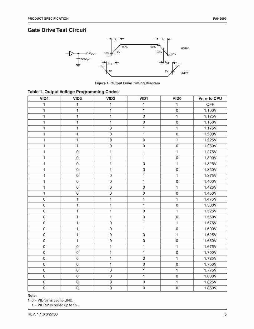
Output Driver Rise & Fall Time See Figure 1, C
L
= 3000pF 20 nsec
Enable/Soft Start
Soft Start Current 10 µAEnable Threshold ON
OFF1.0
0.4V
Power Good
PWRGD Threshold Logic LOW, V
VID
– V
PWRGD
•
85 88 92 %V
OUT
PWRGD Output Voltage I
sink
= 4mA 0.4 VPWRGD Delay High
→
Low 500 µsec
OVP and OTP
Output Overvoltage Detect
•
2.1 2.2 2.3 VOver Temperature Shutdown 130 140 150 °COver Temperature Hysteresis 40 °C
PRODUCT SPECIFICATION FAN5093
REV. 1.1.0 3/27/03 5
Gate Drive Test Circuit
Figure 1. Output Drive Timing Diagram
Table 1. Output Voltage Programming Codes
Note:1. 0 = VID pin is tied to GND. 1 = VID pin is pulled up to 5V.
VID4 VID3 VID2 VID1 VID0 VOUT to CPU
1 1 1 1 1 OFF
1 1 1 1 0 1.100V
1 1 1 0 1 1.125V
1 1 1 0 0 1.150V
1 1 0 1 1 1.175V
1 1 0 1 0 1.200V
1 1 0 0 1 1.225V
1 1 0 0 0 1.250V
1 0 1 1 1 1.275V
1 0 1 1 0 1.300V
1 0 1 0 1 1.325V
1 0 1 0 0 1.350V
1 0 0 1 1 1.375V
1 0 0 1 0 1.400V
1 0 0 0 1 1.425V
1 0 0 0 0 1.450V
0 1 1 1 1 1.475V
0 1 1 1 0 1.500V
0 1 1 0 1 1.525V
0 1 1 0 0 1.550V
0 1 0 1 1 1.575V
0 1 0 1 0 1.600V
0 1 0 0 1 1.625V
0 1 0 0 0 1.650V
0 0 1 1 1 1.675V
0 0 1 1 0 1.700V
0 0 1 0 1 1.725V
0 0 1 0 0 1.750V
0 0 0 1 1 1.775V
0 0 0 1 0 1.800V
0 0 0 0 1 1.825V
0 0 0 0 0 1.850V
tR tF
tDTtDT
HDRV
LDRV2V 2V
10%
3000pF
VOUT2V
90% 90%
2.5V10%

FAN5093 PRODUCT SPECIFICATION
6 REV. 1.1.0 3/27/03
Typical Operating Characteristics(VCC = 12V, VOUT = 1.475V, and TA = +25°C using circuit in Figure 2, unless otherwise noted.)
EFFICIENCY VS. OUTPUT CURRENT
LOAD CURRENT (A)
EF
FIC
IEN
CY
(%
)
HIGH-SIDE GATE DRIVES, RISE / FALL TIME
HIGH-SIDE GATE DRIVES, E*-MODE
ADAPTIVE GATE DELAY
HIGH-SIDE GATE DRIVES, NORMAL OPERATION
LOW-SIDE GATE DRIVES, RISE / FALL TIME
CH1: HDRVBCH2: HDRVA40A Load
CH1: HDRVB40A Load
CH1: HDRVBCH2: HDRVA10A Load
CH1: HDRVBCH2: LDRVB40A Load
CH1: LDRVB40A Load
70
75
80
85
90
0 10 20 30 40 50 60 70 80
2 Phase Mode
E* Mode

PRODUCT SPECIFICATION FAN5093
REV. 1.1.0 3/27/03 7
Typical Operating Characteristics (Continued)
DYNAMIC VID CHANGE
CURRENT LIMIT
CURRENT SHARING, 70A LOAD
OUTPUT RIPPLE, 70A LOAD
CURRENT SHARING, 30A LOAD
DROOP VS. RDROOP
CH1: IL1 (5A/div)CH2: IL2 (5A/div)
CH1: IinCH2: Vout
CH1: IL1 (5A/div)CH2: IL2 (5A/div)
CH1: VOUT (1.475V-1.575V)CH2: VID240A Load
Rdroop (KΩ)
Dro
op
(m
V/A
) (m
Ω)
0.00
0.50
1.00
1.50
2.00
2.50
3.00
0 105 15 20 25 30 35 40
RT = 49.9K
RT = 61.9K

FAN5093 PRODUCT SPECIFICATION
8 REV. 1.1.0 3/27/03
Typical Operating Characteristics (Continued)
START-UP, 40A LOAD
LOAD TRANSIENT, 12-52A
POWER-DOWN, 40A LOAD
LOAD TRANSIENT, 0-40A CH1: Iout (20A/div)CH2: Vout
CH1: Iout (20A/div)CH2: Vout
CH1: VoutCH2: Vin
CH1: Vout CH2: Vin
VOUT TEMPERATURE VARIATION
TEMPERATURE (°C)
1.501
1.500
1.499
1.498
1.497
1.496
1.495
1.4940 25 70 100
VO
UT
(V
)
CLOSED LOOP RESPONSE, 40A LOAD
FREQUENCY (HZ)
GA
IN (
dB
)
PH
AS
E M
AR
GIN
(D
EG
.)
Gain
Phase Margin
-10
0
10
20
30
40
50
100 1000 10000 1000000
30
60
90
120
150
180

PRODUCT SPECIFICATION FAN5093
REV. 1.1.0 3/27/03 9
Application Circuit
Figure 2. Application Circuit for 70A VRM 9.x Desktop Application
Table 2. FAN5093 Application Bill of Materials for Figure 2
Reference QTY Description Manufacturer / Number
U1 1 IC, PWM, FAN5093 Fairchild FAN5093
Q1-8 8 NFET, 30V, 50A, 9mΩ Fairchild FDD6696
D1, 2, 3 3 DIOS, 40V, 500mA Fairchild MBR0540
L1, 2 2 IND, 850nH, 30A, 0.9mΩ Inter-Technical SCTA5022A-R85M
L3 opt IND, 750nH, 20A, 3.5mΩ Inter-Technical SC4015-R75M
R1-4, 9 5 4.7Ω, 5%
R5-8 4 2.2Ω, 5%
R10 1 10Ω, 5%
R11 1 10K, 5%
R12 1 75.0K, 1%
R13 1 13.3K, 1%
R14 1 56.2K, 1%
C1-6 6 1.0µf, 25V, 10%, X7R
C7-10 4 0.1µf, 16V, 10%, X7R
Cin 4 1500µf, 16V, 20%,12mΩ, Aluminum Electrolytic Rubycon 16MBZ1500M
Cout 8 2200µf, 6.3V, 20%, 12mΩ, Aluminum Electrolytic Rubycon 6.3MBZ2200M
+12V
C3
R11
R6
+ Cout
C2
Q5
L2
C7
D3
R2
VID3
Q8
R5
VID4
Q2
Q3
Vin
R1
VID0
R10
C1
VCore
R3
R13
C9
Q6
Q1
C6
R4
R12
R7 Q7
R14
VID1
+ Cin
Vin
FAN5093U1
8
11
12345
24
20
1422
6
12
9
13
17
7
18
15
10
16
23
21
19
LDRVB
HDRVB
VID0VID1VID2VID3VID4
VFB
IL IM
HDRVAENABLE/SS
BYPASS
BOOTB
PGNDB
BOOTA
LDRVA
AGND
VCC
SWA
SWB
PGNDA
RT
DROOP/E*
PWRGD
R9
C8
L1
R8
+5V
L3
C4
Q4
C5
VID2
C10
D2D1

FAN5093 PRODUCT SPECIFICATION
10 REV. 1.1.0 3/27/03
Application Information
OperationThe FAN5093 ControllerThe FAN5093 is a programmable synchronous two-phase DC-DC controller IC. When designed with the appropriate external components, the FAN5093 can be configured to deliver more than 50A of output current, for VRM 9.x applications. The FAN5093 functions as a fixed frequency PWM step down regulator, with a high efficiency mode (E*) at light load.
Main Control LoopRefer to the FAN5093 Block Diagram on page 1. The FAN5093 consists of two interleaved synchronous buck con-verters, implemented with summing-mode control. Each phase has its own current feedback, and there is a common voltage feedback.
The two buck converters controlled by the FAN5093 are interleaved, that is, they run 180° out of phase. This mini-mizes the RMS input ripple current, minimizing the number of input capacitors required. It also doubles the effective switching frequency, improving transient response.
The FAN5093 implements “summing mode control”, which is different from both classical voltage-mode and current-mode control. It provides superior performance to either by allowing a large converter bandwidth over a wide range of output loads and external components. No external compen-sation is required.
The control loop of the regulator contains two main sections: the analog control block and the digital control block. The analog section consists of signal conditioning amplifiers feeding into a comparator which provides the input to the digital control block. The signal conditioning section accepts inputs from a current sensor and a voltage sensor, with the voltage sensor being common to both phases, and the current sensor separate for each. The voltage sensor amplifies the difference between the VFB signal and the reference voltage from the DAC and presents the output to each of the two comparators. The current control path for each phase takes the difference between its PGND and SW pins when the low-side MOSFET is on, reproducing the voltage across the MOSFET and thus the input current; it presents the resulting signal to the same input of its summing amplifier, adding its signal to the voltage amplifier’s with a certain gain. These two signals are thus summed together. This sum is then pre-sented to a comparator looking at the oscillator ramp, which provides the main PWM control signal to the digital control block. The oscillator ramps are 180° out of phase with each other, so that the two phases are on alternately.
The digital control block takes the analog comparator input to provide the appropriate pulses to the HDRV and LDRV
output pins for each phase. These outputs control the external power MOSFETs.
Response TimeThe FAN5093 utilizes leading-edge, not trailing-edge control. Conventional trailing-edge control turns on the high-side MOSFET at a clock signal, and then turns it off when the error amplifier output voltage is equal to the ramp voltage. As a result, the response time of a trailing-edge converter can be as long as the off-time of the high-side driver, nearly an entire switching period. The FAN5093’s leading-edge control turns the high-side MOSFET on when the error amplifier output voltage is equal to the ramp volt-age, and turns it off at the clock signal. As a result, when a transient occurs, the FAN5093 responds immediately by turning on the high-side MOSFET. Response time is set by the internal propagation delays, typically 100nsec. In worst case, the response time is set by the minimum on-time of the low-side MOSFET, 330nsec.
OscillatorThe FAN5093 oscillator section runs at a frequency deter-mined by a resistor from the RT pin to ground according to the formula
The oscillator generates two internal sawtooth ramps, each at one-half the oscillator frequency, and running 180° out of phase with each other. These ramps cause the turn-on time of the two phases to be phased apart. The oscillator frequency of the FAN5093 can be programmed from 200KHz to 2MHz with each phase running at 100KHz to 1MHz, respectively. Selection of a frequency will depend on various system performance criteria, with higher frequency resulting in smaller components but typically lower efficiency.
Remote Voltage SenseThe FAN5093 has true remote voltage sense capability, elim-inating errors due to trace resistance. To utilize remote sense, the VFB and AGND pins should be connected as a Kelvin trace pair to the point of regulation, such as the processor pins. The converter will maintain the voltage in regulation at that point. Care is required in layout of these grounds; see the layout guidelines in this datasheet.
High Current Output DriversThe FAN5093 contains four high current output drivers that utilize MOSFETs in a push-pull configuration. The drivers for the high-side MOSFETs use the BOOT pin for input power and the SW pin for return. The drivers for the low-side MOSFETs use the VCC pin for input power and the PGND pin for return. Typically, the BOOT pin will use a charge pump as shown in Figure 2. Note that the BOOT and VCC pins are separated from the chip’s internal power and ground, BYPASS and AGND, for switching noise immunity.
RT Ω( ) 27.5E9f Hz( )
-------------------=
PRODUCT SPECIFICATION FAN5093
REV. 1.1.0 3/27/03 11
Adaptive Delay Gate DriveThe FAN5093 embodies an advanced design that ensures minimum MOSFET transition times while eliminating shoot-through current. It senses the state of the MOSFETs and adjusts the gate drive adaptively to ensure that they are never on simultaneously. When the high-side MOSFET turns off, the voltage on its source begins to fall. When the voltage there reaches approximately 2.5V, the low-side MOSFETs gate drive is applied. When the low-side MOSFET turns off, the voltage at the LDRV pin is sensed. When it drops below approximately 2V, the high-side MOSFET’s gate drive is applied.
Maximum Duty CycleIn order to ensure that the current-sensing and charge-pumping work, the FAN5093 guarantees that the low-side MOSFET will be on a certain portion of each period. For low frequencies, this occurs as a maximum duty cycle of approxi-mately 90%. Thus at 250KHz, with a period of 4µsec, the low-side will be on at least 4µsec • 10% = 400nsec. At higher frequencies, this time might fall so low as to be ineffective. The FAN5093 guarantees a minimum low-side on-time of approximately 330nsec, regardless of duty cycle.
Current SensingThe FAN5093 has two independent current sensors, one for each phase. Current sensing is accomplished by measuring the source-to-drain voltage of the low-side MOSFET during its on-time. Each phase has its own power ground pin, to per-mit the phases to be placed in different locations without affecting measurement accuracy. For best results, it is impor-tant to connect the PGND and SW pins for each phase as a Kelvin trace pair directly to the source and drain, respec-tively, of the appropriate low-side MOSFET. Care is required in the layout of these grounds; see the layout guidelines in this datasheet.
Current SharingThe two independent current sensors of the FAN5093 operate with their independent current control loops to guarantee that the two phases each deliver half of the total output current. The only mismatch between the two phases occurs if there is a mismatch between the RDS,on of the low-side MOSFETs.
Light Load EfficiencyAt light load, the FAN5093 uses a number of techniques to improve efficiency. Because a synchronous buck converter is two quadrant, able to both source and sink current, during light load the inductor current will flow away from the out-put and towards the input during a portion of the switching cycle. This reverse current flow is detected by the FAN5093 as a positive voltage appearing on the low-side MOSFET during its on-time. When reverse current flow is detected, the low-side MOSFET is turned off for the rest of the cycle, and the current instead flows through the body diode of the high-side MOSFET, returning the power to the source. This technique substantially enhances light load efficiency.
Short Circuit Current Characteristics (ILIM Pin)The FAN5093 short circuit current characteristic includes a function that protects the DC-DC converter from damage in the event of a short circuit. The short circuit limit is set with the RS resistor, as given by the formula
with ISC the desired output current limit, RT the oscillator resistor and RDS,on one phase’s low-side MOSFET’s on resistance. Remember to make the RS large enough to include the effects of initial tolerance and temperature varia-tion on the MOSFETs’ RDS,on.
Important Note! The oscillator frequency must be selected before selecting the current limit resistor, because the value of RT is used in the calculation of RS.
When an overcurrent is detected, the high-side MOSFETs are turned off, and the low-side MOSFETs are turned on, and they remain in this state until the measured current through the low-side MOSFET has returned to zero amps. After reaching zero, the FAN5093 re-soft-starts, ensuring that it can also safely turn on into a short.
A limitation on the current sense circuit is that ISC • RDS,on must be less that 375mV. To ensure correct operation, use ISC • RDS,on ≤ 300mV; between 300mV and 375mV, there will be some non-linearity in the short-circuit current not accounted for in the equation.
As an example, consider the typical characteristic of the DC-DC converter circuit with two FDP6670AL low-side MOSFETs (RDS = 6.5mΩ maximum at 25°C • 1.2 at 75°C = 7.8mΩ each, or 3.9mΩ total) in each phase, RT = 42.1KΩ (600KHz oscillator) and a 50KΩ RS.
The converter exhibits a normal load regulation characteris-tic until the voltage across the MOSFETs exceeds the inter-nal short circuit threshold of 50KΩ/(3.9mΩ • 41.2KΩ • 6.66) = 47A. [Note that this current limit level can be as high as 50KΩ/(3.5mΩ • 41.2KΩ • 6.66) = 52A, if the MOSFETs have typical RDS,on rather than maximum, and are at 25°C.] At this point, the internal comparator trips and signals the controller to leave on the low-side MOSFETs and keep off the high-side MOSFETs. The inductor current decreases, and power is not applied again until the inductor current reaches 0A and the converter attempts to re-softstart.
E*-modeIn addition, further enhancement in efficiency can be obtained by putting the FAN5093 into E*-mode. When the Droop pin is pulled to the 5V BYPASS voltage, the “A” phase of the FAN5093 is completly turned off, reducing in half the amount of gate charge power being consumed. E*-mode can be implemented with the circuit shown in Figure 3.
RS Ω( ) ISC RDS on, RT 3.33•••=

FAN5093 PRODUCT SPECIFICATION
12 REV. 1.1.0 3/27/03
Figure 3. Implementing E*-mode Control
Note: The charge pump for the HIDRVs should be based on the “B” phase of the FAN5093, since the “A” phase is off in E*-mode.
Internal Voltage ReferenceThe reference included in the FAN5093 is a precision band-gap voltage reference. Its internal resistors are precisely trimmed to provide a near zero temperature coefficient (TC). Based on the reference is the output from an integrated 5-bit DAC. The DAC monitors the 5 voltage identification pins, VID0-4, and scales the reference voltage from 1.100V to 1.850V in 25mV steps.
BYPASS ReferenceThe internal logic of the FAN5093 runs on 5V. To permit the IC to run with 12V only, it produces 5V internally with a linear regulator, whose output is present on the BYPASS pin. This pin should be bypassed with a 100nF capacitor for noise suppression. The BYPASS pin should not have any external load attached to it.
Dynamic Voltage AdjustmentThe FAN5093 can have its output voltage dynamically adjusted to accommodate low power modes. The designer must ensure that the transitions on the VID lines all occur simultaneously (within less than 500nsec) to avoid false codes generating undesired output voltages. The Power Good flag tracks the VID codes, but has a 500µsec delay transitioning from high to low; this is long enough to ensure that there will not be any glitches during dynamic voltage adjustment.
Power Good (PWRGD)The FAN5093 Power Good function is designed in accor-dance with the Pentium IV DC-DC converter specifications and provides a continuous voltage monitor on the VFB pin. The circuit compares the VFB signal to the VREF voltage and outputs an active-low interrupt signal to the CPU should the power supply voltage deviate more than -12% of its nom-inal setpoint. The Power Good flag provides no control func-tions to the FAN5093.
Output Enable/Soft Start (ENABLE/SS)The FAN5093 will accept an open collector/TTL signal for controlling the output voltage. The low state disables the output voltage. When disabled, the PWRGD output is in the low state.
Even if an enable is not required in the circuit, this pin should have attached a capacitor (typically 100nF) to soft-start the switching. A softstart capacitor may be approxi-mately chosen by the formula:
where: tD is the delay time before the output starts to ramp
tR is the ramp time of the outputCSS = softstart capVOUT = nominal output voltage
However, C must be ≥ 100nF.
Programmable Active Droop™The FAN5093 features Programmable Active Droop™: as the output current increases, the output voltage drops propor-tionately an amount that can be programmed with an exter-nal resistor. This feature is offered in order to allow maximum headroom for transient response of the converter. The current is sensed losslessly by measuring the voltage across the low-side MOSFET during its on time. Consult the section on current sensing for details. The droop is adjusted by the droop resistor changing the gain of the current loop. Note that this method makes the droop dependent on the temperature and initial tolerance of the MOSFET, and the droop must be calculated taking account of these tolerances. Given a maximum output current, the amount of droop can be programmed with a resistor to ground on the droop pin, according to the formula
with VDroop the desired droop voltage, RT the oscillator resistor, Imax the output current at which the droop is desired, and RDS, on the on-state resistance of one phase’s low-side MOSFET.
Important Note! The oscillator frequency must be selected before selecting the droop resistor, because the value of RT is used in the calculation of RDroop.
Over-Voltage ProtectionThe FAN5093 constantly monitors the output voltage for protection against over-voltage conditions. If the voltage at
FAN5098, Pin 6(Bypass)
FAN5098, Pin 21(Droop, E*)
2N3906
HI=E*MODE 2N3904
1K
10K
10K
10K
RDROOP
tDCSS
10µA--------------
1.7 0.9074 VOUT•+( )2.5
----------------------------------------------------------•=
tRCSS
10µA--------------
VOUT 0.9•VIN
----------------------------•=
RDroop Ω( )VDroop RT•
Imax RDS on,•-------------------------------------=

PRODUCT SPECIFICATION FAN5093
REV. 1.1.0 3/27/03 13
the VFB pin exceeds 2.2V, an over-voltage condition is assumed and the FAN5093 latches on the external low-side MOSFET and latches off the high-side MOSFET. The DC-DC converter returns to normal operation only after VCC has been recycled.
Over Temperature ProtectionIf the FAN5093 die temperature exceeds approximately 150°C, the IC shuts itself off. It remains off until the temper-ature has dropped approximately 25°C, at which time it resumes normal operation.
Component Selection
MOSFET SelectionThis application requires N-channel Enhancement Mode Field Effect Transistors. Desired characteristics are as follows:
• Low Drain-Source On-Resistance, • RDS,ON < 10mΩ (lower is better);• Power package with low Thermal Resistance;• Drain-Source voltage rating > 15V;• Low gate charge, especially for higher frequency
operation.
For the low-side MOSFET, the on-resistance (RDS,ON) is the primary parameter for selection. Because of the small duty cycle of the high-side, the on-resistance determines the power dissipation in the low-side MOSFET and thereforesignificantly affects the efficiency of the DC-DC converter. For high current applications, it may be necessary to use two MOSFETs in parallel for the low-side for each phase.
For the high-side MOSFET, the gate charge is as important as the on-resistance, especially with a 12V input and with higher switching frequencies. This is because the speed of the transition greatly affects the power dissipation. It may be a good trade-off to select a MOSFET with a somewhat higher RDS,on, if by so doing a much smaller gate charge is available. For high current applications, it may be necessary to use two MOSFETs in parallel for the high-side for each phase.
At the FAN5093’s highest operating frequencies, it may be necessary to limit the total gate charge of both the high-side and low-side MOSFETs together, to avert excess power dis-sipation in the IC.
For details and a spreadsheet on MOSFET selection, refer to Applications Bulletin AB-8.
Gate ResistorsUse of a gate resistor on every MOSFET is mandatory. The gate resistor prevents high-frequency oscillations caused by the trace inductance ringing with the MOSFET gate capacitance. The gate resistors should be located physically as close to the MOSFET gate as possible.
The gate resistor also limits the power dissipation inside the IC, which could otherwise be a limiting factor on the switch-ing frequency. It may thus carry significant power, especially at higher frequencies. As an example: The FDB7045L has a maximum gate charge of 70nC at 5V, and an input capaci-tance of 5.4nF. The total energy used in powering the gate during one cycle is the energy needed to get it up to 5V, plus the energy to get it up to 12V:
This power is dissipated every cycle, and is divided between the internal resistance of the FAN5093 gate driver and the gate resistor. Thus,
and each gate resistor thus requires a 1/4W resistor to ensure worst case power dissipation.
Inductor SelectionChoosing the value of the inductor is a tradeoff between allowable ripple voltage and required transient response. A smaller inductor produces greater ripple while producing better transient response. In any case, the minimum induc-tance is determined by the allowable ripple. The first order equation (close approximation) for minimum inductance for a two-phase converter is:
where:Vin = Input Power SupplyVout = Output Voltagef = DC/DC converter switching frequencyESR = Equivalent series resistance of all output capacitors in parallelVripple = Maximum peak to peak output ripple voltage budget.
Schottky Diode SelectionThe application circuit of Figure 2 shows a Schottky diode, D1 (D2 respectively), one in each phase. They are used as free-wheeling diodes to ensure that the body-diodes in the low-side MOSFETs do not conduct when the upper MOSFET is turning off and the lower MOSFETs are turning on. It is undesirable for this diode to conduct because its high forward voltage drop and long reverse recovery time degrades efficiency, and so the Schottky provides a shunt path for the current. Since this time duration is extremely short, being minimized by the adaptive gate delay, the selection criterion for the diode is that the forward voltage of
E QV12---C+ ∆V2• 70nC 5V 1
2---+• 5.4nF 12V 5V–( )2•= =
482nJ=
PRgate
E f Rgate••
Rgate Rinternal+( )------------------------------------------------- 482nJ 300KHz•= =
4.7Ω4.7Ω 0.5Ω+--------------------------------- 131mW=
•
Lmin
Vin 2 V• out–
f-----------------------------------
Vout
Vin----------- ESR
Vripple-----------------••=

FAN5093 PRODUCT SPECIFICATION
14 REV. 1.1.0 3/27/03
the Schottky at the output current should be less than the for-ward voltage of the MOSFET’s body diode. Power capability is not a criterion for this device, as its dissipation is very small.
Output Filter CapacitorsThe output bulk capacitors of a converter help determine its output ripple voltage and its transient response. It has already been seen in the section on selecting an inductor that the ESR helps set the minimum inductance. For most con-verters, the number of capacitors required is determined by the transient response and the output ripple voltage, and these are determined by the ESR and not the capacitance value. That is, in order to achieve the necessary ESR to meet the transient and ripple requirements, the capacitance value required is already very large.
The most commonly used choice for output bulk capacitors is aluminum electrolytics, because of their low cost and low ESR. The only type of aluminum capacitor used should be those that have an ESR rated at 100kHz. Consult Application Bulletin AB-14 for detailed information on output capacitor selection.
For higher frequency applications, particularly those running the FAN5093 oscillator at >1MHz, Oscon or ceramic capaci-tors may be considered. They have much smaller ESR than comparable electrolytics, but also much smaller capacitance.
The output capacitance should also include a number of small value ceramic capacitors placed as close as possible to the processor; 0.1µF and 0.01µF are recommended values.
Input Filter The DC-DC converter design may include an input inductor between the system main supply and the converter input as shown in Figure 2. This inductor serves to isolate the main supply from the noise in the switching portion of the DC-DC converter, and to limit the inrush current into the input capac-itors during power up. A value of 1.3µH is recommended.
It is necessary to have some low ESR capacitors at the input to the converter. These capacitors deliver current when the high side MOSFET switches on. Because of the interleaving, the number of such capacitors required is greatly reduced from that required for a single-phase buck converter. Figure 2 shows 3 x 1500µF, but the exact number required will vary with the output voltage and current, according to the formula
for the two phase FAN5093, where DC is the duty cycle, DC = Vout / Vin. Capacitor ripple current rating is a function of temperature, and so the manufacturer should be contacted to find out the ripple current rating at the expected opera-tional temperature. For details on the design of an input filter, refer to Applications Bulletin AB-16.
Figure 4. Input Filter
Design Considerations and Component SelectionAdditional information on design and component selection may be found in Fairchild’s Application Note 59.
PCB Layout Guidelines• Placement of the MOSFETs relative to the FAN5093 is
critical. Place the MOSFETs such that the trace length of the HIDRV and LODRV pins of the FAN5093 to the FET gates is minimized. A long lead length on these pins will cause high amounts of ringing due to the inductance of the trace and the gate capacitance of the FET. This noise radiates throughout the board, and, because it is switching at such a high voltage and frequency, it is very difficult to suppress.
• In general, all of the noisy switching lines should be kept away from the quiet analog section of the FAN5093. That is, traces that connect to pins 8-17 (LODRV, HIDRV, PGND and BOOT) should be kept far away from the traces that connect to pins 1 through 7, and pins 18-24.
• Place the 0.1µF decoupling capacitors as close to the FAN5093 pins as possible. Extra lead length on these reduces their ability to suppress noise.
• Each power and ground pin should have its own via to the appropriate plane. This helps provide isolation between pins.
• Place the MOSFETs, inductor, and Schottky of a given phase as close together as possible for the same reasons as in the first bullet above. Place the input bulk capacitors as close to the drains of the high side MOSFETs as possible. In addition, placement of a 0.1µF decoupling cap right on the drain of each high side MOSFET helps to suppress some of the high frequency switching noise on the input of the DC-DC converter.
• Place the output bulk capacitors as close to the CPU as possible to optimize their ability to supply instantaneous current to the load in the event of a current transient. Additional space between the output capacitors and the CPU will allow the parasitic resistance of the board traces to degrade the DC-DC converter’s performance under severe load transient conditions, causing higher voltage deviation. For more detailed information regarding capacitor placement, refer to Application Bulletin AB-5.
• A PC Board Layout Checklist is available from Fairchild Applications. Ask for Application Bulletin AB-11.
Irms
Iout
2--------- 2DC 4DC2–=
L3
+12V1000µF, 16VElectrolytic
Vin

PRODUCT SPECIFICATION FAN5093
REV. 1.1.0 3/27/03 15
PC Motherboard Sample Layout and Gerber FileA reference design for motherboard implementation of the FAN5093 along with the PCAD layout Gerber file and silk screen can be obtained through your local Fairchild repre-sentative.
FAN5093 Evaluation BoardFairchild provides an evaluation board to verify the system level performance of the FAN5093. It serves as a guide to performance expectations when using the supplied external components and PCB layout. Please contact your local Fairchild representative for an evaluation board.
Additional InformationFor additional information contact your local Fairchild representative.

FAN5093 PRODUCT SPECIFICATION
16 REV. 1.1.0 3/27/03
Mechanical Dimensions – 24 Lead TSSOP
A — .047 — 1.20
SymbolInches
Min. Max. Min. Max.
MillimetersNotes
A1 .002 .006 0.05 0.15
.012 0.30B .007 0.19
C .004 .008 0.09 0.20
E .169 .177 4.30 4.50
.018 .030 0.45 0.75
.026 BSC 0.65 BSCe
.252 BSC 6.40 BSCH
L
0° 8° 0° 8°
3
5
2
2
N 24 24
αccc .004 0.10— —
D .303 .316 7.70 7.90
Notes:
1.
2.
3.
4.
5.
Dimensioning and tolerancing per ANSI Y14.5M-1982.
"D" and "E" do not include mold flash. Mold flash or protrusions shall not exceed .006 inch (0.15mm).
"L" is the length of terminal for soldering to a substrate.
Terminal numbers are shown for reference only.
Symbol "N" is the maximum number of terminals.
HE
A
D
e
B
A1
– C –
ccc C
LEAD COPLANARITY
SEATINGPLANE
αL
C

FAN5093 PRODUCT SPECIFICATION
3/27/03 0.0m 005Stock#DS30005093
2003 Fairchild Semiconductor Corporation
LIFE SUPPORT POLICY FAIRCHILD’S PRODUCTS ARE NOT AUTHORIZED FOR USE AS CRITICAL COMPONENTS IN LIFE SUPPORT DEVICES OR SYSTEMS WITHOUT THE EXPRESS WRITTEN APPROVAL OF THE PRESIDENT OF FAIRCHILD SEMICONDUCTOR CORPORATION. As used herein:
1. Life support devices or systems are devices or systems which, (a) are intended for surgical implant into the body, or (b) support or sustain life, and (c) whose failure to perform when properly used in accordance with instructions for use provided in the labeling, can be reasonably expected to result in a significant injury of the user.
2. A critical component in any component of a life support device or system whose failure to perform can be reasonably expected to cause the failure of the life support device or system, or to affect its safety or effectiveness.
www.fairchildsemi.com
DISCLAIMER FAIRCHILD SEMICONDUCTOR RESERVES THE RIGHT TO MAKE CHANGES WITHOUT FURTHER NOTICE TO ANY PRODUCTS HEREIN TO IMPROVE RELIABILITY, FUNCTION OR DESIGN. FAIRCHILD DOES NOT ASSUME ANY LIABILITY ARISING OUT OF THE APPLICATION OR USE OF ANY PRODUCT OR CIRCUIT DESCRIBED HEREIN; NEITHER DOES IT CONVEY ANY LICENSE UNDER ITS PATENT RIGHTS, NOR THE RIGHTS OF OTHERS.
Ordering Information
Product Number Description Package
FAN5093MTC VRM 9.x DC-DC Controller 24 pin TSSOP
FAN5093MTCX VRM 9.x DC-DC Controller 24 pin TSSOP in Tape and Reel