Embed Size (px)
Citation preview

Fabrication Processes for Nanomaterials
1
Lecture 5
TOP DOWN
BOTTOM UP

Fabrication MethodsAtom by atom assembly
Like bricklaying, move atoms into place one at a time usingtools like the AFM and STM
Chisel away atomsLike a sculptor, chisel out material from a surface until thedesired structure emerges
Self assemblySet up an environment so atoms assemble automatically.Nature uses self assembly (e.g., cell membranes)
IBM logo assembled from individual xenon atoms
Polystyrenespheres self-assembling
Source: http://www.phys.uri.edu/~sps/STM/stm10.jpg; http://www.nanoptek.com/digitalptm.html
4
Top Down
NANOPARTICLES
5
Mechanical Attrition
Imposing an extremely highdeformation onto the material,structural refinement occurs byshearing and breaking down ofexisting structures and phases
6

Mechanical Attrition – Ball Milling
Schematic diagram of high energy attritor mill
7
Mechanical Attrition – Ball MillingRepeated welding, fracturing and rewelding of particles
8
Mechanical Attrition – Ball MillingControl Factors:
Composition of particles/powders
Size of particles/powders
Milling speed (energy of impact)
Milling temperature
Milling atmosphere
9

Laser AblationAdvantages•Possible high purity of the nanomaterial,•material variety, and the• in situ dispersion of the nanoparticles in a variety ofliquids• allowing safe and stable handling of the colloids.
10
Synthesis of Nanoparticles by PLA in a liquid
To synthesize Ag (Cu2O @ Cu) NPs by PLA, ahigh purity silver (copper) slice is placed onthe bottom of glass vessel containing 20 mlof distilled water.It is irradiated with focused output of 1064nm of pulsed Nd:YAG laser (Spectra PhysicsInc. USA) operating at fixed energy for 30minutes.This results a yellow color in Ag (light greenin Copper) colloidal solution.
Ag Nanoparticles
UV visible absorption spectrum: Theabsorption band at ~398 nm is due toSPR of Ag nanoparticles, confirms theformation of pure Ag nanoparticles.
TEM image of Ag samplesynthesized at 40 mJ/pulse laserenergy confirms formation ofnanoparticles with average particlesize 2-3 nm.
The inset shows SAED pattern,indicates formation of crystallinenanoparticles

Nano-Particle Preparation by PLA (dry)
IEEE International Nanoelectronics Conference 3 8 January 2010 slide 7KMUTT
Lens
Argon gas inlet
Nd YAG Laser ( Miyachi)
(1064 nm, 1 Hz)
Minror
RotatingTarget
Motor
Fig 1. Schematic of pulsed laser ablation on a rotating target
14
15

Bottom UP!
NANOPARTICLES
16
Chemical SynthesisProcesses involving molecular assembly by interactive forcesbetween atoms and molecules, chemical bonds and Van der Waalsforces to form aggregates of atomic and/or molecular units
Major processes: sol gel process and chemical vapour depositionprocess
17
The sol-gel process versatile solution process for making ceramics and glassmaterials. Applying the sol gel process,ultra fine or spherical shaped powders,thin film coatings,ceramic fibers,microporous inorganic membranes, monolithic ceramics andglasses, orextremely porous aerogel materials.

The sol gel process
https://www.llnl.gov/str/May05/Satcher.ht
Possibilities"sol" is cast into a mould,
a wet "gel" will form.
With further drying and heat treatment,the "gel" is converted into dense ceramic or glass articles.
If the liquid in a wet "gel" is removed under a supercriticalcondition,a highly porous and extremely low density material called"aerogel" is obtained.
Aerogel properties can be changed by adding different precursor molecules.
(a) an aluminum oxide foam prepared from aluminum nitrate has a cluster morphology thatresults in
(b) an opaque aerogel.
(c) Using aluminum chloride as the precursor produces an aerogel with fibrous morphology,resulting in
(d) a stronger foam that is also translucent.
https://www.llnl.gov/str/May05/Satcher.ht

Possibilities, cont.Adjust viscosity of a "sol"ceramic fibres can be drawn from the "sol".
Ultra fine and uniform ceramic powdersprecipitation,spray pyrolysis, oremulsion techniques
Limitations of sol gel synthesisPresursorsoften expensivesensitive to moisture
ProcessTime consuming
Dimensional changeshrinkage
Limits largescale
production
cracking
Advantages of sol gel synthesisPrecursorsVolatile
Densification T’s lowChemical conditions mildHighly porous and nanocrystalline materials
Easily purified– high purityproducts

Silica particles produced by sol gel
Colloids

SolutionsHave small particles (ions or molecules)Are transparentDo not separateCannot be filteredDo not scatter light.
A mixture of water H2O and ethanolCH3CH2OH is homogeneous
28
ColloidsCannot be filtered
Do not “settle”
Have medium size particles
Separated with semipermeable membranes
Scatter light (Tyndall effect)Dispersion of matter in size from about 1 1000nm
29
The TyndallEffect
30

Sols – ink, paint
Colloid Examples
Natural aerosols – Fog, clouds
Made aerosol sprays, smogSolid aerosols, smoke, dust
Foam, whipped cream, shaving lather
Emulsions mayonnaise, milk
Gels – Jelly, butter
Pearl
32
Examples of ColloidsFog/smoke
Whipped cream
Milk
Cheese
Blood plasma
Pearls
33

Properties of colloids
Kinetic Properties: Motion of the particleswith respect to the dispersion mediumThermal motionBrownian movementDiffusionOsmosis
Gravity or centrifugal fieldSedimentation
Viscous flow
34
Colloidal dispersions are more stable than suspensions and emulsions, due toSmaller particle size
Brownian movement
In 1889 G.L. Gouy found that the "Brownian" movement was more rapid for smallerparticles (we do not notice Brownian movement of cars, bricks, or people)
35
Spherical colloidal particles of radius 30nm and density 1.35 g cm 3 are suspended in water (at298K, density 1.0 g cm 3, viscosity 1.0x10 3 Pa s).
Calculate the average distance from the origin travelled by a particle in 1 minute due tosedimentation and Brownian motion.
Diffusion distance: Sedimentation distance:
<x2>1/2 = (2Dt)1/2 = (2kTt/6 R)1/2 vt=2R2 gt/9
k = 1.3806488 × 10 23 m2 kg s 2 K 1

Colloids
LyophilicSolvent lovingHydrophilic
LyophobicSolvent hatingHydrophobic
Amphiphillic
Both!!!!
37
Amphophiles
A colloid in which dispersed phase consists ofmicelles.Example: surfactant (surface active agent).
38
Micelles
aggregates of amphophilicmoleculesCritical micelle concentrationConcentration at which micelle isformed
39

40
41
Concentration at the critical micelle concentration.
42

43
Colloids & nanocrystalsNumber of nucleation sites formed initially determines number of particlesproduced› Determined by amount of citrate addedIf initial AuCl4 is kept the same more nucleation sites means final particleswill be smallerFor monodisperse sol need to form nucleation sites quickly andsimultaneously› Hard to do !Gold particles are neutral cores surrounded by AuCl2 ions› Colloid stabilised by electric double layer
44
How can we make nanoparticles?
Mixing hexadecyltrimethylammoniumbromide pentanol micelles of CdCl2with similar micelles containing Na2Sproduces nanoparticle CdS
since the aqueous solution serves as ananoreactor the particles cannotgrow bigger than the micelle
45
Nano films and other structures
46
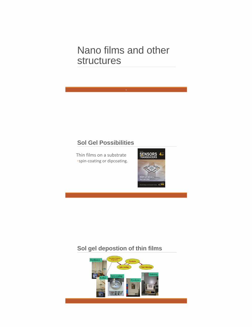
Sol Gel Possibilities
Thin films on a substratespin coating or dipcoating.
Sol gel depostion of thin films

limitations
Spin coatingVariables??
Dip coatingVariables??

Fibre coatingVariables??
Sol gel coatings on particles
SnO2 coated with SiO2,diameter 27nm

Corrosion Protection
Anti-reflective coatings
ELECTROSPINNING

Type I collagen with randomly orientedfibers (left) and aligned fibers (right)
SEM of electrospunelastin at 250 mg/ml.
a) electrospun composite structure (Left),b) SEM of tubular electrospun composite (Middle),c) SEM of electrospun blend of collagen type I, collagen
type III, and elastin (Right)
a) Cotton gauze (left)b) Bovine electrospun fibrinogenmat (right) for potential use as atissue engineering scaffold orwound dressing.
SEM of randomly oriented PLA electrospun fromchloroform (Left) and HFP (Right)
Advanced Drug Delivery Reviews, 59(14), 1413 1433, 2007.
"Diagram by Joanna Gatford at The New Zealand Institute for Plant and Food Research Ltd"
Charge distribution changes
"Diagram by Joanna Gatford at The New Zealand Institute for Plant and Food Research Ltd"

What might control the size of the nano-fibres?
Parameters
1. Molecular weight, molecular weight distribution and architecture (branched,linear etc.) of the polymer
2. Solution properties (viscosity, conductivity and surface tension)
3. Electric potential, flow rate and concentration
4. Distance between the capillary and collection screen
5. Ambient parameters (temperature, humidity and air velocity in the chamber)
6. Motion and size of target screen (collector)
7. Needle gauge

Collectors
Plate
Disc
DrumMandrel
Images courtesy of Mecc Co. Ltd, Fukuoka, Japan
Spinnerets
Clip/tube Tubeless Co axial Heated
Images courtesy of Mecc Co. Ltd, Fukuoka, Japan
Plate - Good for making random mats
Typically, collection area: less than 370cm2 (corresponding to apiece of A5)
Images courtesy of Mecc Co. Ltd, Fukuoka,

DiscCreation of highly aligned fiber sheet
highly aligned fiber sheet can be obtained by the disc collectorcompared to
the drum collector.
Creation of fiber bundle
fiber bundle can be made by this collector.
Typically:Disc circumference: about 600mmRotation Speed : about 63 to 1,890 m/min. (100 to 3,000 rpm)
Images courtesy of Mecc Co. Ltd, Fukuoka, Japan
Drum-Creation of random mesh and aligned fiber sheetThe drum collector can make not only random mesh but alsoaligned fiber sheet.
Function of drum rotation speedRandom mesh – low rotation speedAligned fiber sheet high rotation speed
Typically,Collection area about 1,300cm2 (corresponding to 2 sheets of A4papers)Rotation speed: about 63 to 1,890 m/min. (100 to 3,000 rpm)
Images courtesy of Mecc Co. Ltd, Fukuoka, Japan
Rotating Drum

Mandrel - Creation of tubular nanofibrous assembly
Rod with different diameter can be used as a mandrel.
Possible to create tubular nanofibrous assembly with differentinner diameter.
Attachable Mandrel Diameter : 0.5 to 10 mm
Length of nanofibrous assembly: 150 mm
Images courtesy of Mecc Co. Ltd, Fukuoka,
Clip/Tube
Images courtesy of Mecc Co. Ltd, Fukuoka, Japan

TubelessMinimize waste of solution
The syringe can be directly attached to the spinneret.
No changes of hardware are required to used this spinneret.
Various types of solutions can be electrospun in a short time.
Images courtesy of Mecc Co. Ltd, Fukuoka,
Some Referenceshttp://en.wikipedia.org/wiki/Electrospinning
http://du2012 grp038 01.blogspot.com/2012/04/electrospinning process.html
http://www.people.vcu.edu/~glbowlin/research.html
http://www.people.vcu.edu/~glbowlin/electrospinning.htm
Vapour Deposition Techniques

Plasma and Vapour DepositionProcesses generally involvinga. creation of vapour phase,b. vapour transport from a source to substrate andc. deposition of the vapour phase on the substrate
Two main processes: physical vapour deposition (PVD) andchemical vapour deposition (CVD)
76
Deposition ProcessSchematic diagramshowing theprocesses involvedin nucleation ofdeposited film
78
Comparison of the coating processes

79
Deposition ProcessLayer Mode: growth ofthin layer withcomplete coverage ofthe substrate surface
Island mode: distinctand separate clusters ofthe condensed phasefollowed bycoalescence of theclusters
Mixed mode: formationof a monolayerfollowed by the growthof cluster islands
TWO TYPES OF THIN FILM DEPOSITION: CVD AND PVD -very low gas pressure or high vacuum
CVDReactive gases interactwith substrateUsed to deposit Si anddielectricsGood film qualityGood step coverage
PVDUsed to deposit metalsHigh purityLine of sight
inert gas environment is usually maintained,but reactive gas may be injected into the
chamber for formation of specific compounds
PVDPHYSICAL VAPOUR DEPOSITION

PHYSICAL VAPOUR DEPOSITION (PVD)
Working ConceptPVD processes are carried out under vacuum conditions.The process involved four steps:1. Evaporation2. Transportation3. Reaction4. Deposition
82
Physical Vapor Deposition: PVD
ADVANTAGES: LIMITATIONS:Line of sight
Shadowing
Thickness uniformity
Difficult to evaporate materials with lowvapor pressures
2 types: evaporation and sputtering
Versatile – deposits almostany material
Very few chemical reactions
Little wafer damage
sputtering
84
Microstructure of coatings
SEM images of fractured surface of PVD coatings on nitrided steel: a– monolayer TiN, b– monolayer TiCN and c– multilayer TiAlN
Nucleation and grain growth are involved in coating deposition process on the substrate

85
Nanocomposite coatings (1)
2 phases appear during the deposition process:nanocrystalline AlTiN (hard) and amorphous Si3N4 (tough)
Advantages:• very high nanohardness andtoughness• very high temperature resistance
86
Nanocomposite coatings (2)
Physical Vapour DepositionControl Factors:
1. Energies of emitted atoms/molecules
2. Target to substrate separation and arrangement
3. Chamber pressure and partial pressure of reactive gas
4. Substrate bias voltage and temperature
87

CVDCHEMICAL VAPOUR DEPOSITION
COLORLESS GEMCUT FROMDIAMOND GROWNBY CHEMICALVAPORDEPOS I T ION
Chemical Vapour DepositionMicrofabrication processes widely use CVD to depositmaterials in various forms, including: monocrystalline,polycrystalline, amorphous, and epitaxial.These materials include: silicon, carbon fibre, carbonnanofibres, filaments, carbon nanotubes, SiO2, silicongermanium, tungsten, silicon carbide, silicon nitride,silicon oxynitride and titanium nitride.CVD process is also used to produce synthetic diamonds.
89
Thermal CVD system
http://www.iljinnanotech.co.kr/en/material/r-4-4.htm
Precurser GasFor growing Carbon Nanotubes

Carbon Nanotubes
http://www.iljinnanotech.co.kr/en/material/r-4-4.htm
Chemical Vapour DepositionPrecursor gases are used in the process
A reactive gas/gas mixture is often impinged on the substrate
Process is conducted at a high temperature such that molecularfragments and free atoms are formed and react with reactive gasesto form a desired coating on the substrate
92
Working Concept
Chemical vapor deposition (CVD) results from the chemical reaction of gaseous precursor(s) at aheated substrate to yield a fully dense deposit.
Variables:temperature, pressure, and concentrations
Metal deposition
metal halide (g) metal(s) + byproduct (g)
Ceramic deposition
metal halide (g) + oxygen/carbon/nitrogen/boron source (g) ceramic(s) + byproduct (g)
UNIT IV LECTURE 3 93

Example
Advantages of CVD1. Can be used for a wide range of metals and ceramics2. Can be used for coatings or freestanding structures3. Fabricates net or near net complex shapes4. Is self cleaning—extremely high purity deposits (>99.995% purity)5. Conforms homogeneously to contours of substrate surface6. Has near theoretical as deposited density7. Has controllable thickness and morphology8. Forms alloys9. Infiltrates fiber preforms and foam structures10. Coats internal passages with high length to diameter ratios11. Can simultaneously coat multiple components12. Coats powders
UNIT IV LECTURE 3 96

Issues related to thin film deposition
Quality:CompositionDefect density (e.g. pinholes)ContaminationMechanical and electrical propertiesGood adhesionMinimum stress
TopographyUniform thickness on non planar surfacesStep coverageConformal coverage: uniformSpace filling in holes, channelsVoids
Various types of CVD:
Atmospheric pressure – APCVD
Low pressure – LPCVD
Plasma enhanced – PECVD
High density plasma HDPCVD
Major TechniquesMechanical attrition – top down processRapid condensation and solidificationChemical synthesisPlasma and vapour depositionLithography
101
Laser AblationConventional nanoparticle generation routes•mechanical milling and grinding• drawbacks related to the purity ,
•chemical generation methods like the sol gelprocess•variety of accessible expensive materials.
102