Embed Size (px)
Citation preview

Boulder Summer School
LECTURE 3
Magnetic Junction Devices
Fabricated Magnetic Structures
Yuri Suzuki

Boulder Summer School
Lectures on Fabricated Magnetic Structures
• Introduction• Synthesis and fabrication techniques for magnetic
structures• Magnetic behavior in small magnetic structures• Magnetic Junction Devices
– Patterning of Junction Devices– Spin Polarization– Interfaces
Boulder Summer School
Areal Density of Magnetic HDD and DRAM
AR
EA
L200
2Eh.
PR
Z
Ed Grochowski
1970 1980 1990 2000 2010
Year
10 -2
10 -1
10
10 1
10 2
10 3
10 4
10 5
10 6
Are
al D
ensi
ty, M
bit
s/in
ch2
25% = 2X per 3 years
40 2
60 1.5
100 1
25% CGR
60% CGR
40% CGR
1M4M
16M
64M
256M
1G
3380E
Ultrastar 18XP
Ultrastar XP
3390-2
Ultrastar
36ZXb
Ultrastar 146Z10
100% CGR
Travelstar 40GN
Microdrive II
Travelstar 30GN
512M
2G4G
8G
DRAM projections after 2001 are based on industry capacities and constant chip area
Travelstar 80GN

Boulder Summer School
Lithographic Critical Feature Roadmap forGMR Heads and Semiconductor IC
Robert Fontana
Line
wid
th20
02c.
prz 1980 1990 2000 2010
Year of Production
0.01
0.1
1
10
100
Cri
tica
l Fea
ture
(u
met
ers
)
IC FeaturesIC General
IC GateHead Features
P2wGMRw
P2w
GMRw

Boulder Summer School
Fabricating Magnetic Heterostructureswith length scales below 100nm
• lithographic processes to create small structures fromcontinuousmagnetic multilayers– optical lithography, incl. DUV
– e-beam lithography
– Au particles as milling masks
Liesl FolksHGST

Boulder Summer School
Deep UV lithography
• manufacturable, but slow and expensive• not good for materials testing Marie-Claire Cyrille
HGST

Boulder Summer School
e-beam Lithography
Jordan KatineHGST
resist pillars
vias in AlOx
• fast, expensive, very effective
Boulder Summer School
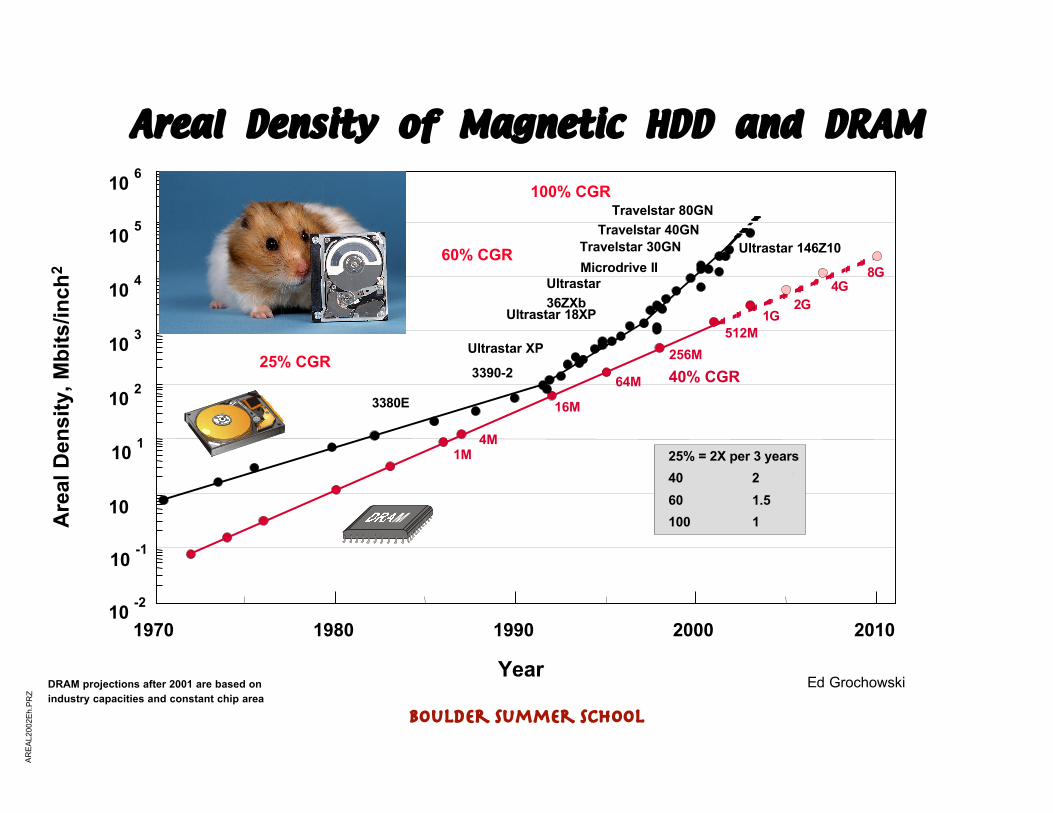
TEM Cross-section ofSpin-transfer Device
alumina
Au
Cu
IrMn 70 ÅCo 50 Å
Cu 40 ÅCo 30 Å
Cu 200 Å
Jordan KatineHGST

Boulder Summer School
Au spheres as milling masksfor creating small pillars
• rapid process for pillar formation:
– attach gold particles (50 - 150 nm) to Au-coated full-film CPPsample
• Lewis et al., JVST B 16 (1998) 2938
– ion mill into MR stack to define pillars
– lift off Au particles
• minimum diameter determined by
layer mill rates and thicknesses
Liesl FolksHGST

Boulder Summer School
Scanning Imaging/Conductance Probe
•imaging of pillars (tapping or contact mode AFM)
•IV curves measured with stationary conducting probe
•tunnel magnetoresistance TMR curves measured with conducting AFM (c-AFM) in applied fields
•require contact + lead resistance < 100 W
•ideally, contact + lead resistance << 100 W
•conductance maps with c-AFM
• Bietsch et al., JVST B 18 1160 (2000)
• Bietsch & Michel, APL 80 3346 (2002)
• Kubota et al., Jpn. JAP 41 L 180 (2002)
• Worledge & Abraham, APL 82 4523 (2003)

Boulder Summer School
AlOx MTJ pillar• good contact (R = 50 W) onexposed PtMn surface
• pillar resistance RJ = 650 WRA = RJ * 0.05 = 32 W mm2
• TMR loop recorded during
30 second field sweep
• c.f. properties measured byconventional means:TMR = 20% and RA = 25 Wmm2
dR / R(10% per div.)
50Field (Oe)
0 100
contact modetopograph conductance map
24 %
Liesl FolksHGST

Boulder Summer School
Au Bead Patterning Technique• Attach Au spheres by decorating CPP magnetic films with colloidal gold particles by immersion into aqueous suspension• Use bifunctional molecular linkers to attach particles to surface• Ar ion milling
• AlOx overcoat and subsequent Au lift-off
Liesl FolksHGST

Boulder Summer School
STO
LSMO (600Å)
Au (1000Å)
Fe3O4
STO
PR
STO
PR PR
STO
SiO2SiO2
SiO2
Junctions are definedby photo lithographyand ion mill.
SiO2 are deposited bylow temperaturesputtering.
• Lift off SiO2
• Expose bottomelectrodes
• Au contact pads are definedby the third mask and afollowing lift off processing.
Fabrication of Magnetic Junctions

Boulder Summer School
Spin Polarized Thin Film Materials
Soulen et al., Science 282, 85 (1998).
Sample
PbSpin polarization as measured by Andreev reflection

Boulder Summer School
Spin Polarization
spin polarized materialsuperconductor spin polarized material
S-I-F junction F-I-F’ junction
superconductor
spin polarized material
Andreev Reflection

Boulder Summer School
Magnetism at Surfaces and Interfaces
• intrinsic nature of ferromagnetism at surfaces and interfaces
Bulk, intermediate length scale (50Å) andsurface (5Å)magnetization are probed bySQUID, magnetic circular dichroism and spinpolarized photo-emission. Park et al. PRL 811953 (1998)
• surface/interface roughness• magnetic domain walls• electrode quality• barrier quality• interface quality

Boulder Summer School
• Meservey-Tedrow junctions(superconductor-insulator-ferromagnet)
CrO2
Al
Parker et al. PRL 88 196601 (02)P=90-94%
• Point contact Andreev reflection Ji et al. PRL 86 5585 (01)
P=96%
Conductance
Voltage
Spin Polarization of CrO2

Boulder Summer School
Spin Polarization of SrRuO3
• Negatively spin-polarized SrRuO3:
D. C. Worledge and T. H. Geballe, PRL 85, 5182 (2000)
T = 0.3K
SrRuO3 50nm
SrTiO3 (100)YBCO 50nm
Al 2nm AlOx
SrTiO31.5nm
H
ÿ A weak negative spinpolarization.
P = -0.095

Boulder Summer School
Magnetic Tunnel Junctions (MTJ)
sP = 1/RP µ N1 N2 + N1 N2
sAP = 1/RAP µ N1 N2 + N1 N2
Tunnel resistance
P =N - N
N + N
Degree of spin polarization
N , N --- densities of majority andminority spin states at Fermi levelJunction
magnetoresistance……
JMR = RAP-RPRAP
JMR = =RAP RP
RAP
2P1P2
1+P1P2
For half metals where P=1, JMR=1 !
Fe3O4/Insulator/Fe3O4
Parallel magnetization
Anti-parallel magnetization
Minority spin band
Majority spin band
JMR
Applied Field

Boulder Summer School
LCMO|NdGaO3|LCMO| epi
Manganite Junctions
Sun et al., APL73, 1008 (1998)Jo et al., PRB61, R14905 (2000)
-3 -2 -1 0 1 2 3
50
100
150 Cool-down A
d.paper.talk.APS.aps98.L100bb1.opj
Single Trace
R (kW
)
H (kOe)
0
100
200
300
Rhigh/Rlow=9.7
Cool-down B
8x2mm2, T=14K
Cool-down A10-Trace Averaged
LSMO|SrTiO3|LSMO| epi

Boulder Summer School
Manganite Junctions
0 100 200 3000
200
400
f.paper.talks.aps99.fig4.opj
Rlow
Rhigh
R (kW
)
T (K)
0.0
1.0
2.0
3.0
Junction size=1x2mm2
DG
(mS)
0.24 0.26 0.28 0.30 0.32
104
105
106
130K
290K
T1/4 (K1/4)
R (W
)
-2 -1 0 1 20.122
0.124
0.126
0.128155K
H (kOe)
0.32
0.36
0.4095KR(
H)
(MW
)
0.26
0.28
0.30
0.3255K
0.30
0.35
0.40
0.45
f.paper.talk.aps.aps99.fig4b.opj
1x2mm2
Ibias=20nA15K
Sun et al., APL 73, 1008 (1998)
Strong decrease of MR upon increasing T.

Boulder Summer SchoolJ. Z. Sun, et al., PRB 61 11244 (2000)
Interface Stability
-4 -2 0 2 446
47
48
49
50
After anneal: +1 mA -1 mA
H (kOe)
-4 -2 0 2 49.0
9.5
10.0
H
T=13.4 K
Before anneal: +1 mA -1 mA
R (
kW)
2
8
• LSMO/STO/Fe junction
• Before/after 220C/15min:
• 5´ increase of RJ.
• Becomes asymmetric
• MR changes sign!
• Junction interface unstable
against moderate heat
treatment.
• Interface FeOx formation!

Boulder Summer School
Manganite Junctions
Cross-sectional TEMof junction 30Å SrTiO3Barrier.
Noh et al. APL 79 234 (01)

Boulder Summer School
CrO2 | Natural barrier | Co trilayers
X. W. Li, Ph. D. Thesis, 1999 (BrownUniv. w. Prof. Gang Xiao and A. Guptaat IBM).
• Observation of an inversemagnetoresistance

Boulder Summer School
Fe3O4/SrTiO3/(La,Sr)MnO3 Junctions
Ghosh et al., APL 73, 689 (1998).

Boulder Summer School
Fe3O4 based Epitaxial Oxide MTJs
Li et al. APL 73 3282 (1998)
van der Zaag et al.JMMM 211 301 (2001)
MR of 1.5% at 150K and <1% at 190K • small coercivity difference• tunnel barrier choicePoly Fe3O4 junctions (Panchula et al. unpublished )• JMR= -44% at low T
Fe3O4 MgO

Boulder Summer School
Magnetic Tunnel Junctions (MTJ)
Minority spin band
Majority spin band
Low resistance
Fe3O4/Insulator/Fe3O4
High resistance
Parallel magnetization
Anti-parallel magnetization
Anti-parallel magnetization
Parallel magnetization
Fe3O4/Insulator/La0.7Sr0.3MnO3
Resistance
Applied Field
Resistance
Applied Field

Boulder Summer School
3.32105
3.486105
3.652105
3.818105
3.984105
-20
-15
-10
-5
0
-4000 -2000 0 2000 4000
MR (%
)
0
-10
Field (kOe)0 2 4
-20-2-4
Magnetoresistance andMagnetics in OxideJunctions
• well defined parallel and antiparallelstates• magnetoresistance as high as 30%
R(kΩ
)
400
380
0-1000 1000Field (Oe)
Mag
neti c
mom
ent
( mem
u )
0
3
Fe3O4 (800Å)
La0.7Sr0.3MnO3 (600Å)
CoCr2O4 (60Å)
SrTiO3 substrate

Boulder Summer School
I-V characteristics of the MTJ
-1000
-500
0
500
1000
0
1
2
3
4
5
6
-500 0 500Bias Voltage [mV]
T=200KC
urre
nt (
mA
)C
onductance [mW
-1]
ß By fitting the I-V data with Simmons’s tunnel equation forintermediate-voltage range (V<j0/e), we obtain the following results:j0 = 1.0eV, d = 20Å

Boulder Summer School
Hopping Transport in Oxide Junctions
0
1
2
3
4
0 50 100 150 200 250 300 350 400
0.042
0.044
0.046
0.048
0.05
0.052
0 7 14 21 28 350 14 28
0.052
0.050
0.048
0.046
0.046
Cond
uct a
nce
( mΩ
-1)
Bias (mV)
Bias (mV)
GS= Gdir+Gres+SGNhop[V]N-2/(N+1)
Cond
uct a
nce
( mΩ
- 1)
• Inelastic hopping through localizedstates in the CoCr2O4 barrier• Hopping through 2 states inthe barrier fits well at low biaseswhile hopping through 2 or 3 statesfits well over a larger bias range
N=2 and 3
N=2
N

Boulder Summer School
Spin Polarization of Fe3O4
• Spin polarized photoemission studies of Fe3O4: P=-40% at 10K Alvarado et al. PRL 34 319 (75)
P=-80% at RT Dedkov et al. PRB 65 64417 (02)
P=-55% at RT Huang et al. JMMM 239 261 (02)
• Fitting high temperature MR(T) to magnon excitations: P=Po(1-aT3/2)
0
5
10
15
20
25
30
35
0 50 100 150 200 250 300
MRSpin Polarization
0
-10
-20
-30
0 100 200 300
MR (%)Spin Polarization (%)
Temperature (K)
T [K]P[
%]
-
-
-
-
-
-
P0 = -39%
P=P0(1-aT3/2)*
10
15
20
25
30
35
100 120 140 160 180 200 220 240 260
Pth=-67% at 0KSrinitiwarawong et al. J.Phys.Cond.Matter 13 7987 (01)

Boulder Summer School
Low temperature peak due to …..• Verwey transition of Fe3O4• Magnetic transition of the CoCr2O4 barrier
High T ->Higher MR Low T->Lower MR
0
5
10
15
20
25
30
35
0 50 100 150 200 250 300
MRSpin Polarization
0
-10
-20
-30
0 100 200 300
MR (%)Spin Polarization (%)
Temperature (K)
Spin Polarization of Fe3O4

Boulder Summer School
Field-effect-transistor with manganite channel
• three terminal device based on manganites
• carrier modulation through PZT gate
T. Wu et al., PRL86, 5998 (2001).
Boulder Summer School
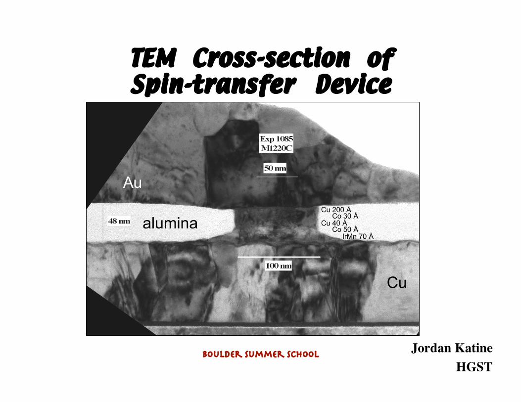
Oxide Devices: Sensors
Stuart Parkin and Jonathan Sun, IBM
Sensor length scaleswith track width
• Sub-100nm scaling of MR headschallenge existing technology:– GMR: too low in resistance to give
enough signal.– MTJ: too resistive. Shot noise hurts
S/N.• Can oxide MR elements fill the
gap???+ Large MR.+ Intermediate resistance.- 300 K performance?- Switching field control?- Noise characteristics in deep sub-
micron region?- Processing compatibility?

Boulder Summer School
Acknowledgements
• Liesl Folks, Hitachi Global Storage Tech.• Jordan Katine, Hitachi Global Storage Tech.• Caroline Ross, MIT• Jonathan Sun, IBM Yorktown Heights• Guohan Hu, Hitachi Global Storage Tech.