Embed Size (px)
Citation preview

www.EVGroup.com
EVG SmartNIL® Technology for Patterning
Requirements of More than Moore Applications
Dr. Martin Eibelhuber

www.EVGroup.com EV Group Confidential and Proprietary
Outline
Introduction
SmartNIL ®
Application Focus
Inspire
2

www.EVGroup.com EV Group Confidential and Proprietary
EVGroup
EVG is a global supplier of:
Wafer Bonders
Mask Aligners
Coaters / Developers /Cleaners
Temporary Bonders / Debonders
Inspection / Metrology Systems
Nanoimprint Lithography System
EV Group holds the dominant share of the market for wafer bonding equipment
and is a technology leader in lithography for advanced packaging and
nanotechnology.
3
www.EVGroup.com EV Group Confidential and Proprietary
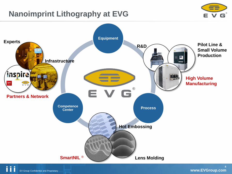
Nanoimprint Lithography at EVG
4
EVG Nanoimprint
Equipment
Process Competence
Center
High Volume
Manufacturing
Experts Pilot Line &
Small Volume
Production
Hot Embossing
Lens Molding SmartNIL ®
Infrastructure
Partners & Network
R&D

www.EVGroup.com EV Group Confidential and Proprietary
Nanoimprint Lithography at a Glance
Micro Contact Printing
(µCP) Soft Lithography Hot Embossing SmartNIL (UV-NIL)
5
Thermoplastic materials;
bulk polymer or spin-on
UV curing polymers with
photo initiator
(Bio-) Functionalized
materials and glues
www.EVGroup.com EV Group Confidential and Proprietary
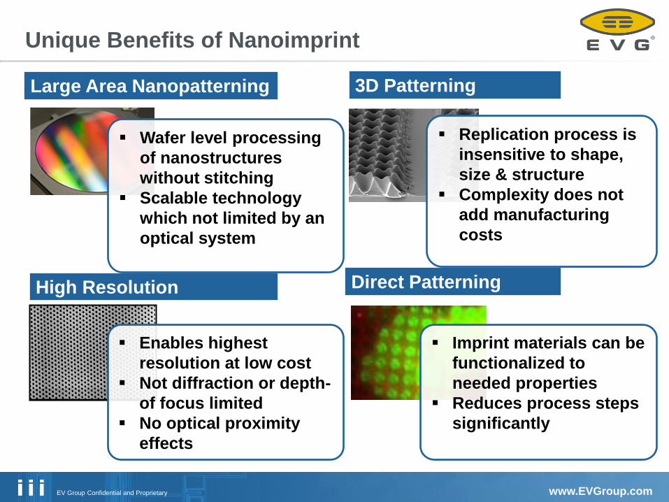
Unique Benefits of Nanoimprint
Large Area Nanopatterning
High Resolution
3D Patterning
Direct Patterning
Enables highest
resolution at low cost
Not diffraction or depth-
of focus limited
No optical proximity
effects
Wafer level processing
of nanostructures
without stitching
Scalable technology
which not limited by an
optical system
Replication process is
insensitive to shape,
size & structure
Complexity does not
add manufacturing
costs
Imprint materials can be
functionalized to
needed properties
Reduces process steps
significantly

www.EVGroup.com EV Group Confidential and Proprietary
EVG SmartNIL® Product Family
SmartNIL® - Features:
Room-Temperature Process | UV-Curable Resist
Wafer Size up to 8” | Gen2 Panel Size
Robust and Field-Proven Proprietary SmartNIL® Technology
Flexible Soft Stamp | Simple & Fast Stamp Fabrication Process
Permanent Functional Layers Achievable
High Fidelity Replication | High Dimensional Uniformity
SmartNIL® - Equipment:
R&D multi-purpose systems
Automated stand-alone systems
Integrated systems
Panel-size systems

www.EVGroup.com EV Group Confidential and Proprietary
SmartNIL® Capabilities
8
SmartNIL®
Resolution
Aspect Ratio
CD Uniformity
Scalability
CD Evolution
Flexibility
www.EVGroup.com EV Group Confidential and Proprietary
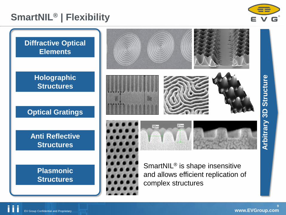
SmartNIL® | Flexibility
9
Optical Gratings
Plasmonic
Structures
Arb
itra
ry 3
D S
tru
ctu
re
Anti Reflective
Structures
Holographic
Structures
Diffractive Optical
Elements
SmartNIL® is shape insensitive
and allows efficient replication of
complex structures

www.EVGroup.com EV Group Confidential and Proprietary
Optical Sensing
Source:Yole
Wafer level processing enables:
Smallest form factors,
High performance
Cost efficient manufacturing
More than Moore devices
require novel pattering methods
to achieve economy of scale
www.EVGroup.com EV Group Confidential and Proprietary
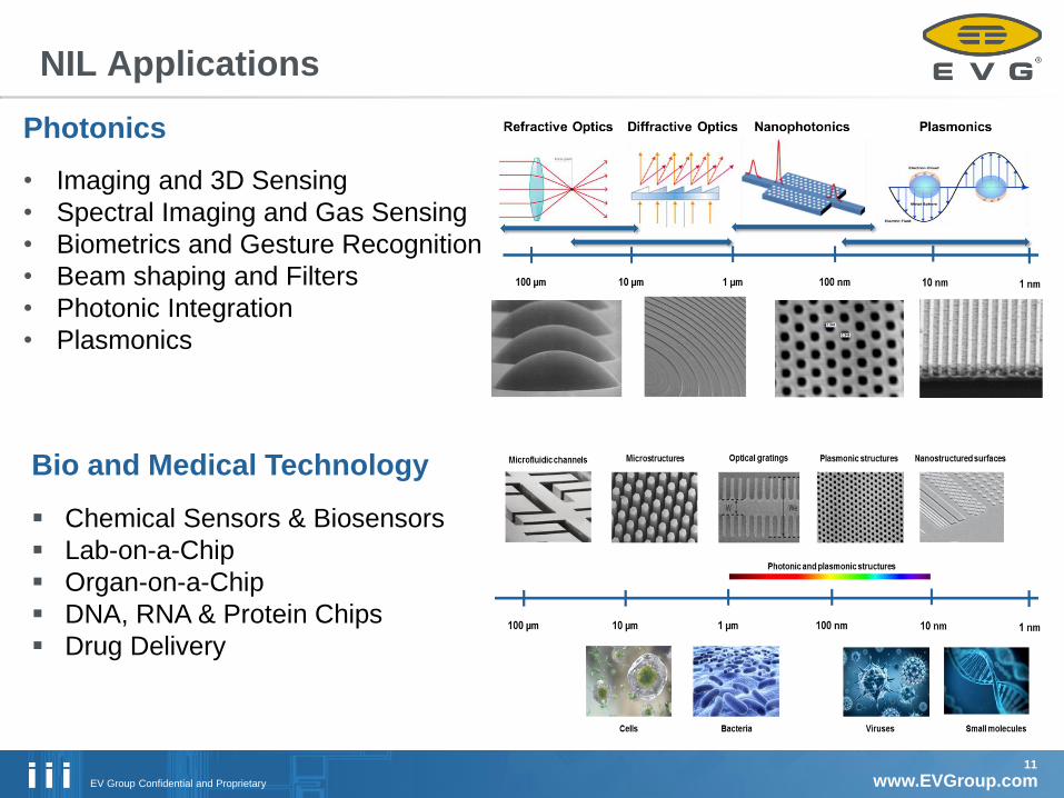
NIL Applications
11
Photonics
• Imaging and 3D Sensing
• Spectral Imaging and Gas Sensing
• Biometrics and Gesture Recognition
• Beam shaping and Filters
• Photonic Integration
• Plasmonics
Bio and Medical Technology
Chemical Sensors & Biosensors
Lab-on-a-Chip
Organ-on-a-Chip
DNA, RNA & Protein Chips
Drug Delivery
www.EVGroup.com EV Group Confidential and Proprietary
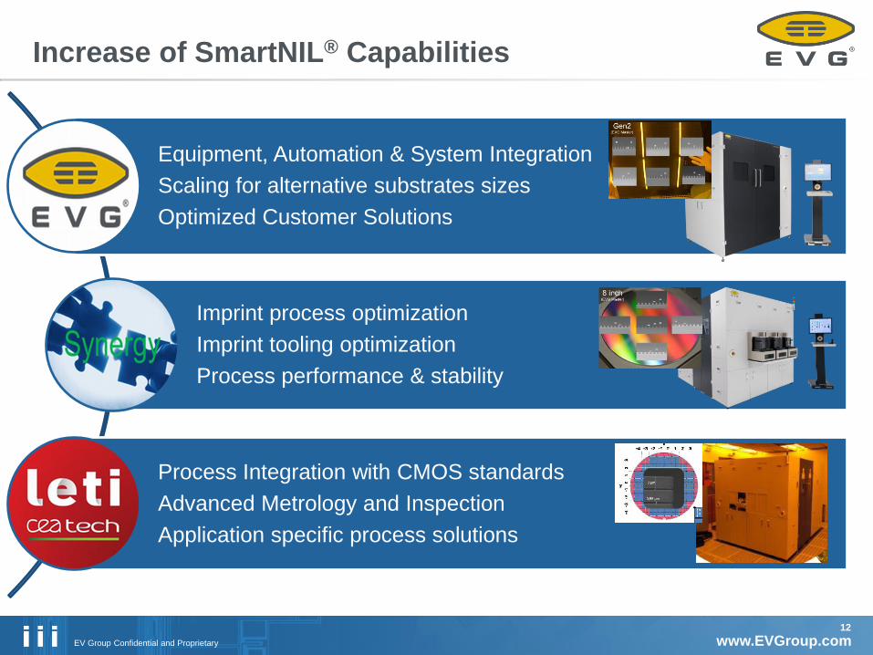
Increase of SmartNIL® Capabilities
12
Equipment, Automation & System Integration
Scaling for alternative substrates sizes
Optimized Customer Solutions
Imprint process optimization
Imprint tooling optimization
Process performance & stability
Process Integration with CMOS standards
Advanced Metrology and Inspection
Application specific process solutions

www.EVGroup.com EV Group Confidential and Proprietary
Key Takeaways
Targets
Enabling novel devices and applications
Fully CMOS compatible production line
Goals
Imprint Technology Improvement
Platform Improvements
Process Integration
Addressed Topics
Overlay, Yield, Material Influence
Automation, Process Monitoring, Performance
Etching, Deposition, Mix and match Lithography
Wafer-level Nanoimprint Lithography SmartNIL ® is established for photonic, bio and backend-like manufacturing
Proven capabilities Equipment Readiness Addressing
Challenges Beyond

www.EVGroup.com EV Group Confidential and Proprietary
Data, design and specifications may not simultaneously apply; or depend on individual equipment configuration, process conditions and materials and may vary accordingly. EVG reserves the right to
change data, design and specifications without prior notice. All trademarks, logos, website addresses or equipment names that contain the letters or words "EVG" or "EV Group" or any combination thereof,
as well as the following names and acronyms are registered trademarks and/or the property of EV Group: ComBond®, CoverSpinTM, EZB®, EZ Bond®, EZD®, EZ Debond®, EZR®, EZ Release®, GEMINI®,
HERCULES®, HyperIntegration®, IQ Aligner®, LowTempTM, NanoAlign®, NanoFillTM, NanoSprayTM, NIL-COM®, NILPhotonics®, OmniSpray®, SmartEdge®, SmartView®, The Triple "i" Company Invent-
Innovate-Implement®, Triple i®. Other product and company names may be registered trademarks of their respective owners.
Dr. Martin Eibelhuber
Deputy Business Development
Thank You!