Embed Size (px)
Citation preview

Evaluation of the Teledyne SIDECAR ASIC at cryogenic temperature using a visible hybrid H2RG focal plane array in 32 channel readout
mode
Reinhold J. Dorn*1, Siegfried Eschbaumer1, Donald N.B. Hall2, Gert Finger1, Leander Mehrgan1 , Manfred Meyer1and Joerg Stegmeier1
1European Southern Observatory, Karl-Schwarzschild Str.2, D-85748 Garching, Germany 2Institute for Astronomy, 640 N. A`ohoku Place, Hilo, HI 96720, USA
ABSTRACT
Teledyne Imaging Sensors (TIS) has developed a new CMOS device known as the SIDECAR application-specific integrated circuit (ASIC). This single chip provides all the functionality of FPA drive electronics to operate visible and infrared imaging detectors with a fully digital interface. At the last SPIE conference we presented test and performance results of a Teledyne 2K×2K silicon PIN diode array hybridized to a Hawaii-2RG multiplexer, the Hybrid Visible Silicon Imager (HyViSI). This detector was read out with the ESO standard IR detector controller IRACE, which delivers detector limited performance. We have now tested the H2RG HyViSI detector with the new TIS SIDECAR ASIC in 32 channel readout mode at cryogenic temperatures. The SIDECAR has been evaluated down to 105 Kelvin operating temperature and performance results have been compared to those obtained with external electronics. We find that the SIDECAR ASIC provides performance equal to optimized external electronics.
Keywords: ASIC, SIDECAR, Conversion gain, interpixel capacitance, CMOS hybrid, quantum efficiency, Hawaii-2RG, Si-PIN, HyViSI, IR detectors, HgCdTe
1. INTRODUCTION At ESO and in most astronomical applications external control electronics is used to control detectors in the visible and infrared wavelength range. The recent controllers used at ESO have been FIERA and IRACE which are planned to be replaced by a new design called the New General Detector Controller (NGC) [Meyer et. al. 2005]. Teledyne Imaging Sensors offers an alternative to discrete external electronics, the SIDECAR ASIC. This Application-Specific Integrated Circuit (ASIC) includes all capabilities to operate focal plane arrays on a single chip. This ASIC will be used to control detectors on the James Webb Space telescope and will be used to repair the ACS camera on the Hubble Space Telescope, reading out CCD devices. ESO has purchased the SIDECAR ASIC for test purposes and built a test system reading a Teledyne Hawaii-2RG detector to demonstrate the SIDECAR’s performance for ground-based astronomy. The detector we have tested with the ASIC is a Teledyne 2K×2K silicon PIN diode array hybridized to a Hawaii-2RG multiplexer, the Hybrid Visible Silicon Imager (HyViSI). The detector is an optical sensor, analogous to near-infrared (NIR) array detectors. The separation of photon collection from readout facilitates separate optimization of the readout integrated circuit (ROIC) and the detector array. The main difference to IR detectors is that for silicon PIN the full bulk of the detector material is depleted whereas IR detectors are depleted only in the region of the p-n junction. Note that a hybrid differs substantially from a monolithic CMOS imager. In a monolithic CMOS imager, both readout and photon detection take place in the same piece of silicon. As nearly the full bulk of the detector is in depletion, silicon PIN detectors have good QE at both red and blue wavelengths. This Silicon PIN detector is operated at a high bias voltage (~10 Volt) compared to near-IR detectors. This detector has been extensively tested in 2006 (Dorn et. al., 2006) in 32 channel mode with the ESO external detector controller IRACE, and its performance is now being compared to the results obtained with the SIDECAR ASIC. The use of this kind of optical detector also simplified strongly the cryostat design and the turnaround time for warming up and cooling down cycles, as the detector and ASIC only needed to be cooled to ~105 Kelvin for optimum performance. *[email protected]; phone +49-89-32006547; fax +49-89-3202362; www.eso.org/~rdorn
2. SIDECAR ASIC ARCHITECTURE The SIDECAR ASIC is a fully programmable control and digitization system for analog image sensors. It operates from room temperature to cryogenic temperatures as low as 30 K. Figure 1 shows a block diagram of a typical ASIC detector system. The top block represents the detector, which is connected to the ASIC via analog and digital lines. At the bottom of the ASIC block, only digital connections go to the external data acquisition system. Due to the immunity of the digital signal transmission which can be LVDS or CMOS, the back end system can be located several meters from the ASIC. The basic SIDECAR architecture, as shown in the diagram, can be divided into the following major blocks: analog bias generator, A/D converter, digital control and timing generation, data memory and processing, and digital data interface [Loose et al. 2003].
Figure 1 Block Diagram of the SIDECAR ASIC (Picture credit M. Loose)
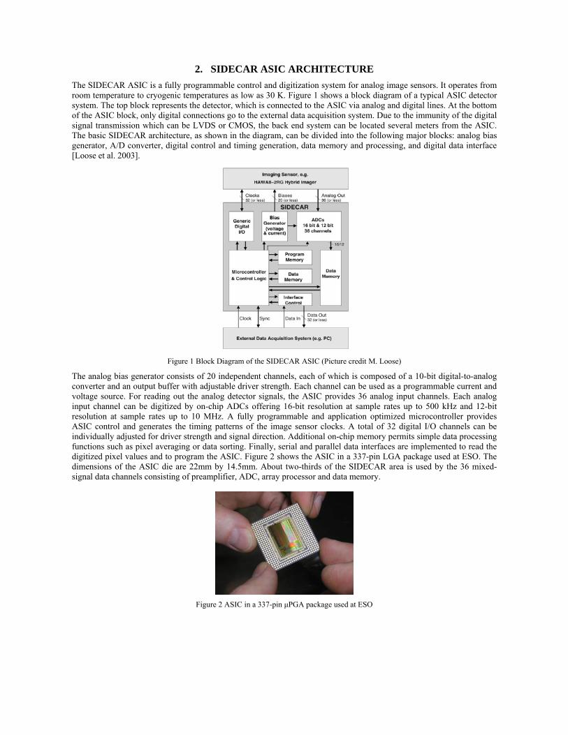
The analog bias generator consists of 20 independent channels, each of which is composed of a 10-bit digital-to-analog converter and an output buffer with adjustable driver strength. Each channel can be used as a programmable current and voltage source. For reading out the analog detector signals, the ASIC provides 36 analog input channels. Each analog input channel can be digitized by on-chip ADCs offering 16-bit resolution at sample rates up to 500 kHz and 12-bit resolution at sample rates up to 10 MHz. A fully programmable and application optimized microcontroller provides ASIC control and generates the timing patterns of the image sensor clocks. A total of 32 digital I/O channels can be individually adjusted for driver strength and signal direction. Additional on-chip memory permits simple data processing functions such as pixel averaging or data sorting. Finally, serial and parallel data interfaces are implemented to read the digitized pixel values and to program the ASIC. Figure 2 shows the ASIC in a 337-pin LGA package used at ESO. The dimensions of the ASIC die are 22mm by 14.5mm. About two-thirds of the SIDECAR area is used by the 36 mixed-signal data channels consisting of preamplifier, ADC, array processor and data memory.
Figure 2 ASIC in a 337-pin μPGA package used at ESO
A summary of the most important ASIC properties is given below. Focal Plane Control and Read-Out Capability:
• 36 analog input channels • Up to 500 kHz A/D conversion with 16 bit resolution per channel • Up to 10 MHz A/D conversion with 12 bit resolution per channel • Preamp gain = 0dB …27 dB in steps of 3dB • 32 programmable digital I/O (clock generation) • 20 programmable bias voltages/currents • 16 bit microcontroller • Efficient power-down modes • 1-24 parallel digital output channels for data transfer (LVDS or CMOS)
Reduced System Space, Weight and Power:
• < 100 mW at 100 kHz 32 – channel operation • Chip dimensions ~ 22mm x 15 mm using deep submicron CMOS processing • Only requires one power supply, one fixed reference and one master clock for operation
3. SIDECAR ASIC SETUPS AT ESO 3.1 Warm setup with development board
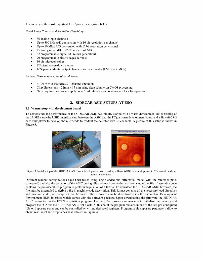
To demonstrate the performance of the SIDECAR ASIC we initially started with a warm development kit consisting of the JADE2 card (the USB2 interface card between the ASIC and the PC), a warm development board and a Hawaii-2RG bare multiplexer to develop the microcode to readout the detector with 32 channels. A picture of this setup is shown in Figure 3.
Figure 3 Initial setup of the SIDECAR ASIC on a development board reading a Hawaii-2RG bare multiplexer in 32 channel mode at
room temperature
Different readout configurations have been tested using single ended and differential mode (with the reference pixel connected) and also the behavior of the ASIC during idle and exposure modes has been studied. A file of assembly code contains the pre-assembled program to perform acquisition of a H2RG. To download the SIDECAR ASIC firmware, the file must be assembled to derive a file in machine code description. This format contains all the necessary load directives and machine code that comprises the firmware. The firmware can be downloaded via the Interactive Development Environment (IDE) interface which comes with the software package. Upon downloading the firmware the SIDECAR ASIC begins to run the H2RG acquisition program. The very first program sequence is to initialize the memory and program the SCA via the SIDECAR ASIC SPI block. At this point the program remains in one of the two pre-configured Idle or Exposure states and can be controlled by writing dedicated registers. Programmable exposure parameters allow to obtain read, reset and drop fames as illustrated in Figure 4.
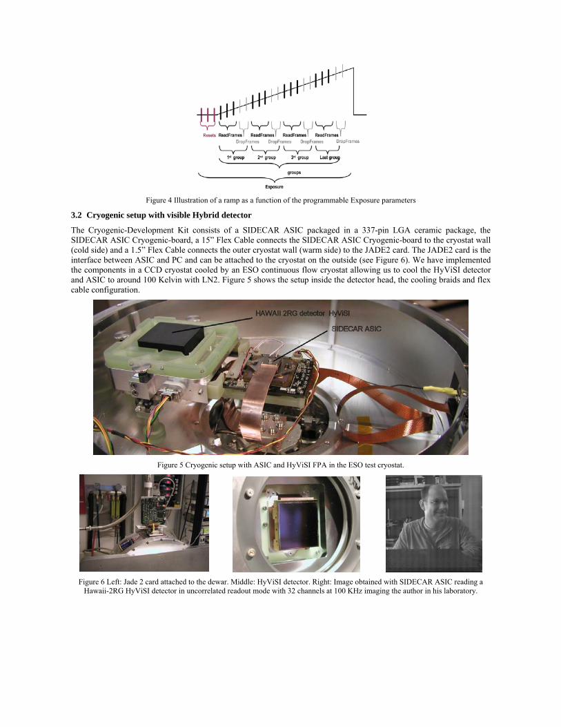
Figure 4 Illustration of a ramp as a function of the programmable Exposure parameters
3.2 Cryogenic setup with visible Hybrid detector
The Cryogenic-Development Kit consists of a SIDECAR ASIC packaged in a 337-pin LGA ceramic package, the SIDECAR ASIC Cryogenic-board, a 15” Flex Cable connects the SIDECAR ASIC Cryogenic-board to the cryostat wall (cold side) and a 1.5” Flex Cable connects the outer cryostat wall (warm side) to the JADE2 card. The JADE2 card is the interface between ASIC and PC and can be attached to the cryostat on the outside (see Figure 6). We have implemented the components in a CCD cryostat cooled by an ESO continuous flow cryostat allowing us to cool the HyViSI detector and ASIC to around 100 Kelvin with LN2. Figure 5 shows the setup inside the detector head, the cooling braids and flex cable configuration.
Figure 5 Cryogenic setup with ASIC and HyViSI FPA in the ESO test cryostat.
Figure 6 Left: Jade 2 card attached to the dewar. Middle: HyViSI detector. Right: Image obtained with SIDECAR ASIC reading a
Hawaii-2RG HyViSI detector in uncorrelated readout mode with 32 channels at 100 KHz imaging the author in his laboratory.

After some initial setup problems we obtained our first image in uncorrelated read mode imaging the author with ASIC and HyViSI operating at 110 Kelvin. We used all 32 channels reading at a pixel rate of 100 KHz and 16 bit resolution. 3.3 Initial setup modifications
In the default configuration using the JADE2 card connected to the USB2 port of a laptop or PC and the standard JADE2 jumper configuration the image shows some very strong pickup noise over a broad band of frequencies. Especially some low frequencies produce a strong pattern as seen in Figure 7 (left). We investigated a couple of options to reduce this pickup. The most effective modifications are to supply the analog 5V power to the JADE2 card with a clean voltage from a linear power supply and to electrically insulate the USB connection with a fiber link to the PC. Also the USB converter should be operated with a linear power supply to reduce pickup noise. Finally some improvement can be seen by grounding the ASIC backplane (substrate) to analog ground on the ASIC cryogenic board. Fine-tuning of the operating voltages (for both the detector and the internal voltages for the preamp) and some microcode optimization lead to a performance of 2.7 electrons readout noise, leaving a very clean image as shown in Figure 7 (right). The next sections will explain the steps to optimize the ASIC for low noise operation in more detail.
Figure 7 Various DCS images during optimization of the ASIC and HyViSI array for low noise operation (see text above)
4. CONVERSION FACTOR 4.1 FE-55 measurements and conversion factor
Usually the nodal capacitance C0 of a detector pixel can be calculated from the slope of a plot of noise squared signal versus mean signal, the photon transfer curve [Janesick]. However, this method only works if the signals of neighboring pixels are uncorrelated. Current HyViSI detectors suffer from interpixel coupling which smooths the image and attenuates Poisson noise, introducing an error of up to 50 % for the conversion factor measured with the signal versus noise method. In the past, this led to wrong values by determining the QE of the detector by almost 100% [Dorn, 2006]. Hence, we measure the conversion factor for the HyViSI read by the ASIC with an Fe-55 X-ray source. Fe-55 is a radioactive source that emits X-rays at three energy levels. The emission is caused by the inner electron of the Fe-55 isotope being captured by the nucleus, transforming it into Manganese. The first emissions is at 5.9 keV (Mn Kα line), the second but weaker peak at 6.5 keV (Mn Kβ) and the third at 4.12 keV (Kα escape line). When these X-rays are absorbed by silicon they produce large photoelectron events. Each Kα event generates 1620 electrons, Kβ 1778 electrons and the Kα escape peak 1133 electrons. All of these X-rays are easily stopped with glass or metal. To perform the test with the HyViSI detector, a plexiglas window with a thickness of 2 mm was used not to attenuate the X-rays too much to allow enough events on the detector. An Fe-55 source with 1 MBq was used and installed on a special window (see Figure 8). Moreover to obtain the nodal capacitance C0 by a direct measurement which does not rely on statistical methods, a simple but very powerful technique has been developed. It is based on comparing the voltage change of a large calibrated external capacitor to that of the unknown nodal capacitance C0 which is many orders of magnitudes smaller [Finger et al., 2005]. For the HyViSI detector a nodal capacitance 13.9 fF was measured [Dorn, 2006]. The discrepancy of nodal capacitances C0 determined by the capacitance comparison and the shot noise method are substantial and about a factor of two for the HyViSI detector. Thus, plausible quantum efficiencies cannot be achieved using the conversion gain derived from the shot noise method with the usual “noise squared versus signal” technique. The capacitance comparison method confirms the values measured with the Fe-55 measurements and leads to the
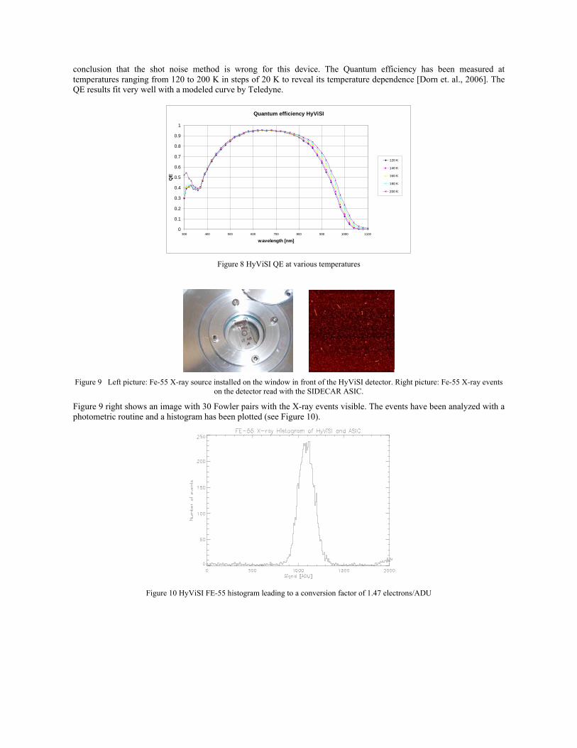
conclusion that the shot noise method is wrong for this device. The Quantum efficiency has been measured at temperatures ranging from 120 to 200 K in steps of 20 K to reveal its temperature dependence [Dorn et. al., 2006]. The QE results fit very well with a modeled curve by Teledyne.
Quantum efficiency HyViSI
0
0.1
0.2
0.3
0.4
0.5
0.6
0.7
0.8
0.9
1
300 400 500 600 700 800 900 1000 1100
wavelength [nm]
QE
120 K
140 K
160 K
180 K
200 K
Figure 8 HyViSI QE at various temperatures
Figure 9 Left picture: Fe-55 X-ray source installed on the window in front of the HyViSI detector. Right picture: Fe-55 X-ray events
on the detector read with the SIDECAR ASIC.
Figure 9 right shows an image with 30 Fowler pairs with the X-ray events visible. The events have been analyzed with a photometric routine and a histogram has been plotted (see Figure 10).
Figure 10 HyViSI FE-55 histogram leading to a conversion factor of 1.47 electrons/ADU
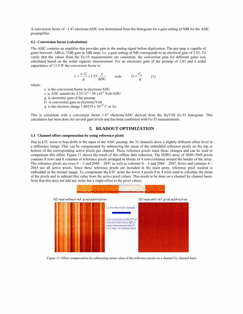
A conversion factor of ~1.47 electrons/ADU was determined from the histogram for a gain setting of 9dB for the ASIC preamplifier. 4.2 Conversion factor (calculation)
The ASIC contains an amplifier that provides gain to the analog signal before digitization. The pre-amp is capable of gains between -3dB to 27dB gain in 3dB steps. I.e. a gain setting of 9db corresponds to an electrical gain of 2.83. To verify that the values from the Fe-55 measurements are consistent, the conversion gain for different gains was calculated based on the nodal capacity measurement. For an electronic gain of the preamp of 2.83 and a nodal capacitance of 13.9 fF the conversion factor is:
with (1)
where:
c is the conversion factor in electrons/ADU s is ADC sensitivity 3.3V/216= 50 x10-6 Volt/ADU g is electronic gain of the preamp G is conversion gain in electrons/Volt q is the electron charge 1.60218 x 10⁻¹⁹ C or As
This is consistent with a conversion factor 1.47 electrons/ADU derived from the HyViSI Fe-55 histogram. This calculation has been done for several gain levels and has been confirmed with Fe-55 measurements.
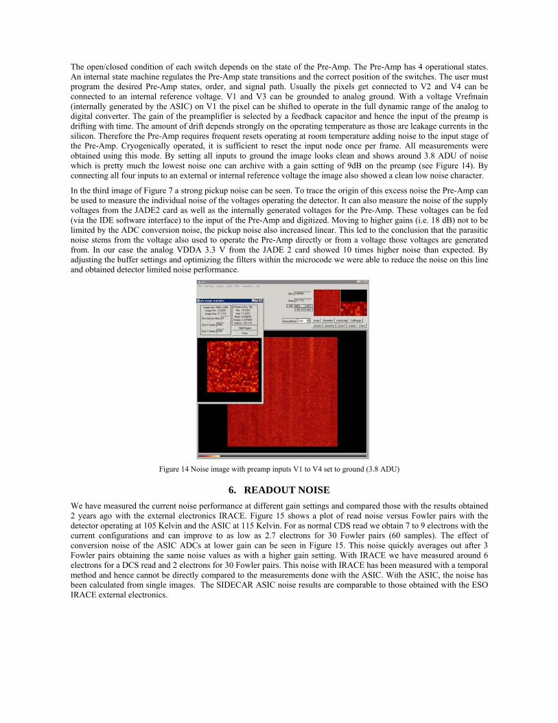
5. READOUT OPTIMIZATION 5.1 Channel offset compensation by using reference pixels
Due to kTC noise or bias drifts at the input of the ASIC preamp, the 32 channels show a slightly different offset level in a difference image. This can be compensated by subtracting the mean of the embedded reference pixels on the top or bottom of the corresponding active pixels per channel. These reference pixels track those changes and can be used to compensate this offset. Figure 11 shows the result of this offline data reduction. The H2RG array of 2048×2048 pixels contains 8 rows and 8 columns of reference pixels arranged in blocks of 4 rows/columns around the border of the array. The reference pixels are rows 0 – 3 and 2044 – 2047 as well as columns 0 – 3 and 2044 – 2047. Rows and columns 4 – 2043 are all active pixels. Since these reference pixels are included in the main array, reference pixel readout is embedded in the normal image. To compensate the kTC noise the lower 4 pixels 0 to 4 were used to calculate the mean of the pixels and to subtract this value from the active pixel values. This needs to be done on a channel by channel basis. Note that this does not add any noise but a slight offset to the pixel values.
Figure 11 Offset compensation by subtracting mean value of the reference pixels on a channel by channel basis
ADUe
gGsc 53.1=⋅
=q
CG 0=

5.2 Large offset of HyViSI reference pixels compared to those for HgCdTe H2RG arrays
The H2RG HyViSI operates nearly identically to H2RG HgCdTe, except for the Vsub and Dsub biases. Vsub is a bias unique to silicon detector. It is the detector substrate bias and signal return of all pixel diodes (~10V). Dsub is connected to the p+ side of a guard detector ring located along the perimeter of the array. Guard ring pixels have the same polarity as active pixels. They provide an electric field boundary to the edge pixels. Dsub gets adjusted equal to Vrst (~0.06V). This is illustrated in Figure 12. The reference pixels have a much higher capacitance than the HyVisi pixels. Therefore, the charge injection at the end of a reset shows up as a different voltage depending on the capacitance. This makes it very difficult to adjust both (reference pixels and active pixels) to be in the range of the ADC and hence limits the dynamic range, especially at high gain. A solution to this can be implemented by not using the reference pixels but a voltage internally generated by the ASIC (i.e. Vref1 or Vref2) as a reference input to the ASIC preamp for the first and last four rows of the device. This voltage can be adjusted to have the offset value in the range of the ADCs at various gains settings. As this voltage also tracks the KTC noise it can be used to compensate these offsets as well as the reference pixels. This has been implemented in the microcode and is used at high gain settings. However one disadvantage is that the substrate voltage is different (ref. pixels are connected to Dsub, HyViSi pixels are connected to Vsub > 10 V), the reference pixels do not track the noise of Vsub. That is why they are less efficient compared to HgCdTe detectors with respect to noise reduction.
E-Field
Active pixels
Silicon PIN detector
VSUB voltage
H2RG multiplexer
Reference pixels Guard ring detector
Dsub
Vrst
Photons
p+
n+
Figure 12 HyViSI Reference pixels - functional diagram. Vsub is the detector substrate (10 V) and Dsub is connected to the guard
ring (Dsub at Vreset level)
5.3 ASIC preamp functional diagram
Figure 13 shows a simplified schematic representation of the Preamplifier of the SIDECAR ASIC.
Figure 13 ASIC preamp functional diagram
The open/closed condition of each switch depends on the state of the Pre-Amp. The Pre-Amp has 4 operational states. An internal state machine regulates the Pre-Amp state transitions and the correct position of the switches. The user must program the desired Pre-Amp states, order, and signal path. Usually the pixels get connected to V2 and V4 can be connected to an internal reference voltage. V1 and V3 can be grounded to analog ground. With a voltage Vrefmain (internally generated by the ASIC) on V1 the pixel can be shifted to operate in the full dynamic range of the analog to digital converter. The gain of the preamplifier is selected by a feedback capacitor and hence the input of the preamp is drifting with time. The amount of drift depends strongly on the operating temperature as those are leakage currents in the silicon. Therefore the Pre-Amp requires frequent resets operating at room temperature adding noise to the input stage of the Pre-Amp. Cryogenically operated, it is sufficient to reset the input node once per frame. All measurements were obtained using this mode. By setting all inputs to ground the image looks clean and shows around 3.8 ADU of noise which is pretty much the lowest noise one can archive with a gain setting of 9dB on the preamp (see Figure 14). By connecting all four inputs to an external or internal reference voltage the image also showed a clean low noise character.
In the third image of Figure 7 a strong pickup noise can be seen. To trace the origin of this excess noise the Pre-Amp can be used to measure the individual noise of the voltages operating the detector. It can also measure the noise of the supply voltages from the JADE2 card as well as the internally generated voltages for the Pre-Amp. These voltages can be fed (via the IDE software interface) to the input of the Pre-Amp and digitized. Moving to higher gains (i.e. 18 dB) not to be limited by the ADC conversion noise, the pickup noise also increased linear. This led to the conclusion that the parasitic noise stems from the voltage also used to operate the Pre-Amp directly or from a voltage those voltages are generated from. In our case the analog VDDA 3.3 V from the JADE 2 card showed 10 times higher noise than expected. By adjusting the buffer settings and optimizing the filters within the microcode we were able to reduce the noise on this line and obtained detector limited noise performance.
Figure 14 Noise image with preamp inputs V1 to V4 set to ground (3.8 ADU)
6. READOUT NOISE We have measured the current noise performance at different gain settings and compared those with the results obtained 2 years ago with the external electronics IRACE. Figure 15 shows a plot of read noise versus Fowler pairs with the detector operating at 105 Kelvin and the ASIC at 115 Kelvin. For as normal CDS read we obtain 7 to 9 electrons with the current configurations and can improve to as low as 2.7 electrons for 30 Fowler pairs (60 samples). The effect of conversion noise of the ASIC ADCs at lower gain can be seen in Figure 15. This noise quickly averages out after 3 Fowler pairs obtaining the same noise values as with a higher gain setting. With IRACE we have measured around 6 electrons for a DCS read and 2 electrons for 30 Fowler pairs. This noise with IRACE has been measured with a temporal method and hence cannot be directly compared to the measurements done with the ASIC. With the ASIC, the noise has been calculated from single images. The SIDECAR ASIC noise results are comparable to those obtained with the ESO IRACE external electronics.

0
1
2
3
4
5
6
7
8
9
10
1 10 100
Readout noise[electrons]
Number of Fowler pairs
Readout noise of HyViSI array and ASIC as a function of Fowler pairs
Noise in electrons/105K (ASIC), gain=2.8, conversion factor =1.47 e/ADU Noise in electrons/105K (ASIC) ,gain=8, conversion factor = 0.54 e/ADU Figure 15 Read noise as a function of Fowler pairs for two different gain settings
Figure 16 shows CDS images obtained with the ASIC operating the HyViSI detector under the same conditions and operating voltages as with our external electronics. Additionally a noise histogram for the array is shown. Figure 17 shows the images and histogram for measurements done with 30 Fowler pairs.
Figure 16 Noise image and Histogram for HyViSI and ASIC for a correlated double sample (7 electrons readout noise)
Figure 17 Noise image and Histogram for HyViSI and ASIC for a 30 Fowler pair read (2.7 electrons readout noise)
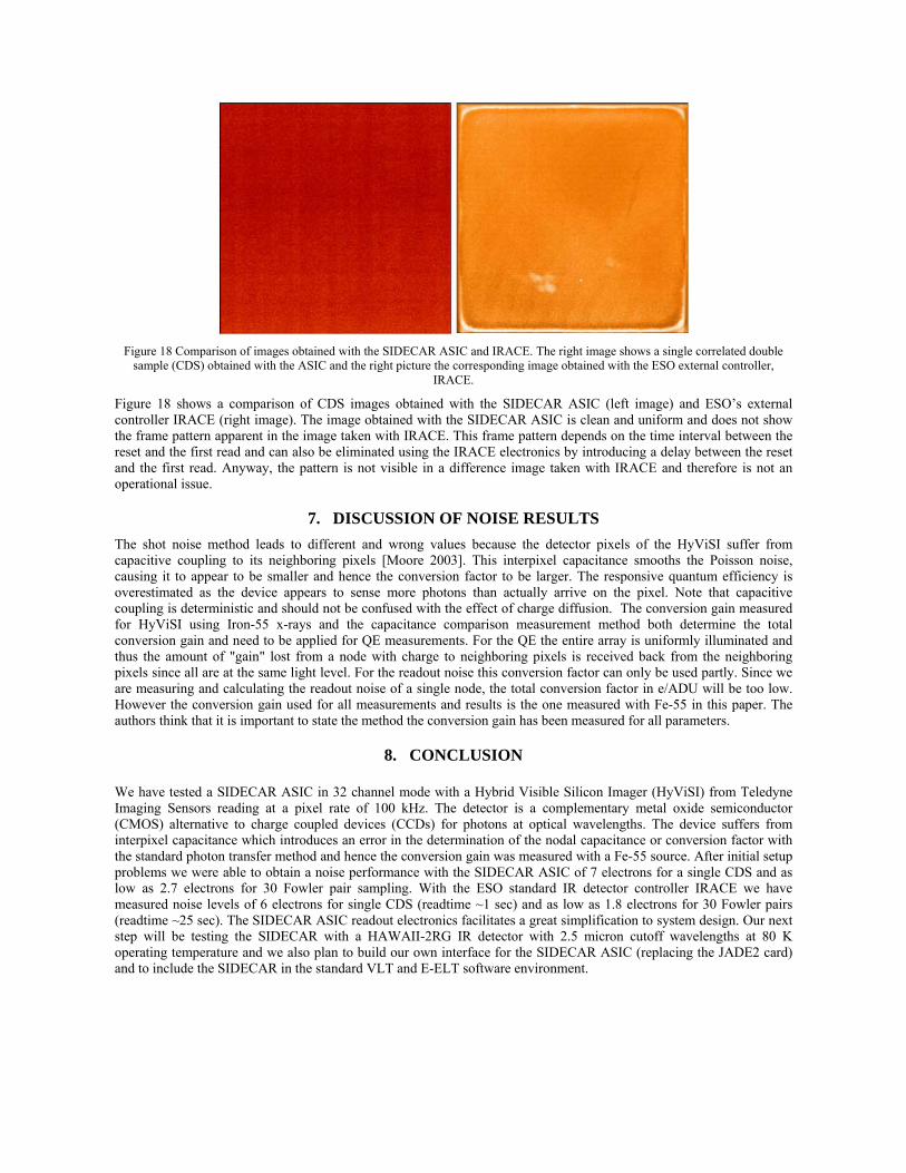
Figure 18 Comparison of images obtained with the SIDECAR ASIC and IRACE. The right image shows a single correlated double
sample (CDS) obtained with the ASIC and the right picture the corresponding image obtained with the ESO external controller, IRACE.
Figure 18 shows a comparison of CDS images obtained with the SIDECAR ASIC (left image) and ESO’s external controller IRACE (right image). The image obtained with the SIDECAR ASIC is clean and uniform and does not show the frame pattern apparent in the image taken with IRACE. This frame pattern depends on the time interval between the reset and the first read and can also be eliminated using the IRACE electronics by introducing a delay between the reset and the first read. Anyway, the pattern is not visible in a difference image taken with IRACE and therefore is not an operational issue.
7. DISCUSSION OF NOISE RESULTS The shot noise method leads to different and wrong values because the detector pixels of the HyViSI suffer from capacitive coupling to its neighboring pixels [Moore 2003]. This interpixel capacitance smooths the Poisson noise, causing it to appear to be smaller and hence the conversion factor to be larger. The responsive quantum efficiency is overestimated as the device appears to sense more photons than actually arrive on the pixel. Note that capacitive coupling is deterministic and should not be confused with the effect of charge diffusion. The conversion gain measured for HyViSI using Iron-55 x-rays and the capacitance comparison measurement method both determine the total conversion gain and need to be applied for QE measurements. For the QE the entire array is uniformly illuminated and thus the amount of "gain" lost from a node with charge to neighboring pixels is received back from the neighboring pixels since all are at the same light level. For the readout noise this conversion factor can only be used partly. Since we are measuring and calculating the readout noise of a single node, the total conversion factor in e/ADU will be too low. However the conversion gain used for all measurements and results is the one measured with Fe-55 in this paper. The authors think that it is important to state the method the conversion gain has been measured for all parameters.
8. CONCLUSION
We have tested a SIDECAR ASIC in 32 channel mode with a Hybrid Visible Silicon Imager (HyViSI) from Teledyne Imaging Sensors reading at a pixel rate of 100 kHz. The detector is a complementary metal oxide semiconductor (CMOS) alternative to charge coupled devices (CCDs) for photons at optical wavelengths. The device suffers from interpixel capacitance which introduces an error in the determination of the nodal capacitance or conversion factor with the standard photon transfer method and hence the conversion gain was measured with a Fe-55 source. After initial setup problems we were able to obtain a noise performance with the SIDECAR ASIC of 7 electrons for a single CDS and as low as 2.7 electrons for 30 Fowler pair sampling. With the ESO standard IR detector controller IRACE we have measured noise levels of 6 electrons for single CDS (readtime ~1 sec) and as low as 1.8 electrons for 30 Fowler pairs (readtime ~25 sec). The SIDECAR ASIC readout electronics facilitates a great simplification to system design. Our next step will be testing the SIDECAR with a HAWAII-2RG IR detector with 2.5 micron cutoff wavelengths at 80 K operating temperature and we also plan to build our own interface for the SIDECAR ASIC (replacing the JADE2 card) and to include the SIDECAR in the standard VLT and E-ELT software environment.

9. ACKNOWLEDGMENTS
All tests have been performed in the ESO infrared detector lab. The author would like to thank Markus Loose, James Beletic, Raphael Ricardo and Richard Blank from Teledyne Imaging Sensors for their help getting the SIDECAR ASIC working in 32 channel mode and for many useful discussions.
10. REFERENCES 1. M. Loose, L. Lewyn, H. Durmus, J. Garnett, D. Hall, A Joshi, L. Kozlowski and I. Ovsiannikov, “SIDECAR
lowpower control ASIC for focal plane arrays incl. A/D conversion and bias generation”, Instrument Design and Perform. for Optical/IR Ground-based Telescopes, Proc. SPIE, Vol. 4841, pp. 782-794, 2003.
2. Gert Finger, James W. Beletic, Reinhold J. Dorn, Manfred Meyer, Leander Mehrgan, Alan F. Moorwood and Joerg Stegmeier, Conversion gain and interpixel capacitance of CMOS hybrid focal plane arrays, Workshop on Scientific Detectors for Astronomy, Springer-Verlag, (2005).
3. Manfred Meyer et. al., NGC Detector Array Controller Based on a high speed serial link technology, Proc. Scientific Detectors for Astronomy 2005, eds. Jenna E. Beletic, P. Amico and J. W. Beletic, Astrophysics and Space Library, (2005)
4. J. R. Janesick, Scientific Charge-Coupled Devices, SPIE Press, p. 134, (2001). 5. Reinhold J. Dorn, S. Eschbaumer, G. Finger, L. Mehrgan, M. Meyer and J. Stegmeier, A CMOS Visible Silicon
Imager hybridized to a Rockwell 2RG multiplexer as a new detector for ground based astronomy - European Southern Observatory (ESO), Germany; in the proceedings of the "SPIE's International Symposium on Astronomical Telescopes and Instrumentation 2006, Orlando, Florida,; 24 - 31 May 2006, SPIE publications, vol. 6267, High Energy, Optical, and Infrared Detectors for Astronomy II (2006).
6. Gert Finger, James Garnett, Naidu Bezawada, Reinhold J. Dorn, Leander Mehrgan, Manfred Meyer, Alan Moorwood, Joerg Stegmeier and Guy Woodhouse, Performance evaluation and calibration issues of large format hybrid active pixel sensors used for ground and space based astronomy, Nuclear Inst. and Methods in Physics Research A, (2005)
7. A. Moore et al, QE Overestimation and Deterministic Crosstalk Resulting from Inter-pixel Capacitance, Opt. Eng. (2003).