Embed Size (px)
Citation preview
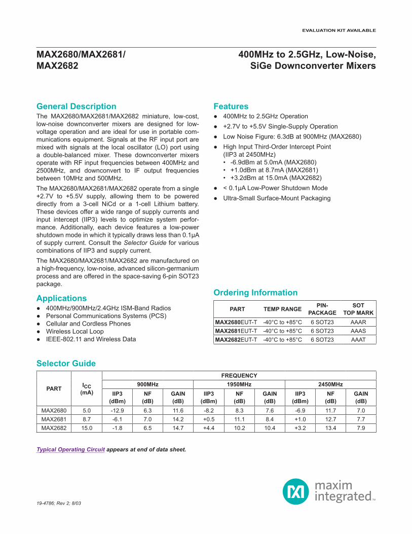
General DescriptionThe MAX2680/MAX2681/MAX2682 miniature, low-cost, low-noise downconverter mixers are designed for low-voltage operation and are ideal for use in portable com-munications equipment. Signals at the RF input port are mixed with signals at the local oscillator (LO) port using a double-balanced mixer. These downconverter mixers operate with RF input frequencies between 400MHz and 2500MHz, and downconvert to IF output frequencies between 10MHz and 500MHz.The MAX2680/MAX2681/MAX2682 operate from a single +2.7V to +5.5V supply, allowing them to be powered directly from a 3-cell NiCd or a 1-cell Lithium battery. These devices offer a wide range of supply currents and input intercept (IIP3) levels to optimize system perfor-mance. Additionally, each device features a low-power shutdown mode in which it typically draws less than 0.1μA of supply current. Consult the Selector Guide for various combinations of IIP3 and supply current.The MAX2680/MAX2681/MAX2682 are manufactured on a high-frequency, low-noise, advanced silicon-germanium process and are offered in the space-saving 6-pin SOT23 package.
Applications 400MHz/900MHz/2.4GHz ISM-Band Radios Personal Communications Systems (PCS) Cellular and Cordless Phones Wireless Local Loop IEEE-802.11 and Wireless Data
Features 400MHz to 2.5GHz Operation +2.7V to +5.5V Single-Supply Operation Low Noise Figure: 6.3dB at 900MHz (MAX2680) High Input Third-Order Intercept Point
(IIP3 at 2450MHz) • -6.9dBm at 5.0mA (MAX2680) • +1.0dBm at 8.7mA (MAX2681) • +3.2dBm at 15.0mA (MAX2682)
< 0.1μA Low-Power Shutdown Mode Ultra-Small Surface-Mount Packaging
19-4786; Rev 2; 8/03
Typical Operating Circuit appears at end of data sheet.
PART TEMP RANGE PIN- PACKAGE
SOTTOP MARK
MAX2680EUT-T -40°C to +85°C 6 SOT23 AAARMAX2681EUT-T -40°C to +85°C 6 SOT23 AAASMAX2682EUT-T -40°C to +85°C 6 SOT23 AAAT
PART ICC(mA)
FREQUENCY900MHz 1950MHz 2450MHz
IIP3(dBm)
NF(dB)
GAIN(dB)
IIP3(dBm)
NF(dB)
GAIN(dB)
IIP3(dBm)
NF(dB)
GAIN(dB)
MAX2680 5.0 -12.9 6.3 11.6 -8.2 8.3 7.6 -6.9 11.7 7.0MAX2681 8.7 -6.1 7.0 14.2 +0.5 11.1 8.4 +1.0 12.7 7.7MAX2682 15.0 -1.8 6.5 14.7 +4.4 10.2 10.4 +3.2 13.4 7.9
MAX2680/MAX2681/MAX2682
400MHz to 2.5GHz, Low-Noise,SiGe Downconverter Mixers
Selector Guide
Ordering Information
EVALUATION KIT AVAILABLE
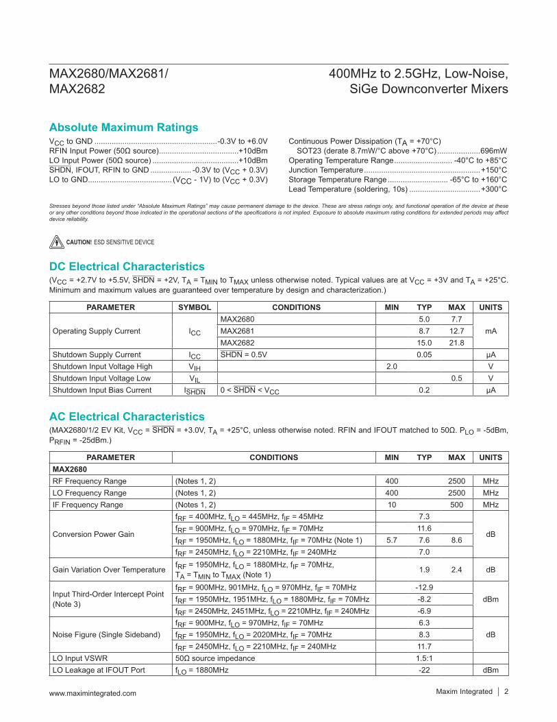
VCC to GND .........................................................-0.3V to +6.0VRFIN Input Power (50Ω source) .....................................+10dBmLO Input Power (50Ω source) ........................................+10dBmSHDN, IFOUT, RFIN to GND ................... -0.3V to (VCC + 0.3V)LO to GND....................................... (VCC - 1V) to (VCC + 0.3V)
Continuous Power Dissipation (TA = +70°C) SOT23 (derate 8.7mW/°C above +70°C) ....................696mW
Operating Temperature Range ........................... -40°C to +85°CJunction Temperature ......................................................+150°CStorage Temperature Range ............................ -65°C to +160°CLead Temperature (soldering, 10s) .................................+300°C
(MAX2680/1/2 EV Kit, VCC = SHDN = +3.0V, TA = +25°C, unless otherwise noted. RFIN and IFOUT matched to 50Ω. PLO = -5dBm, PRFIN = -25dBm.)
(VCC = +2.7V to +5.5V, SHDN = +2V, TA = TMIN to TMAX unless otherwise noted. Typical values are at VCC = +3V and TA = +25°C. Minimum and maximum values are guaranteed over temperature by design and characterization.)
PARAMETER SYMBOL CONDITIONS MIN TYP MAX UNITS
Operating Supply Current ICC
MAX2680 5.0 7.7mAMAX2681 8.7 12.7
MAX2682 15.0 21.8Shutdown Supply Current ICC SHDN = 0.5V 0.05 μAShutdown Input Voltage High VIH 2.0 VShutdown Input Voltage Low VIL 0.5 VShutdown Input Bias Current ISHDN 0 < SHDN < VCC 0.2 μA
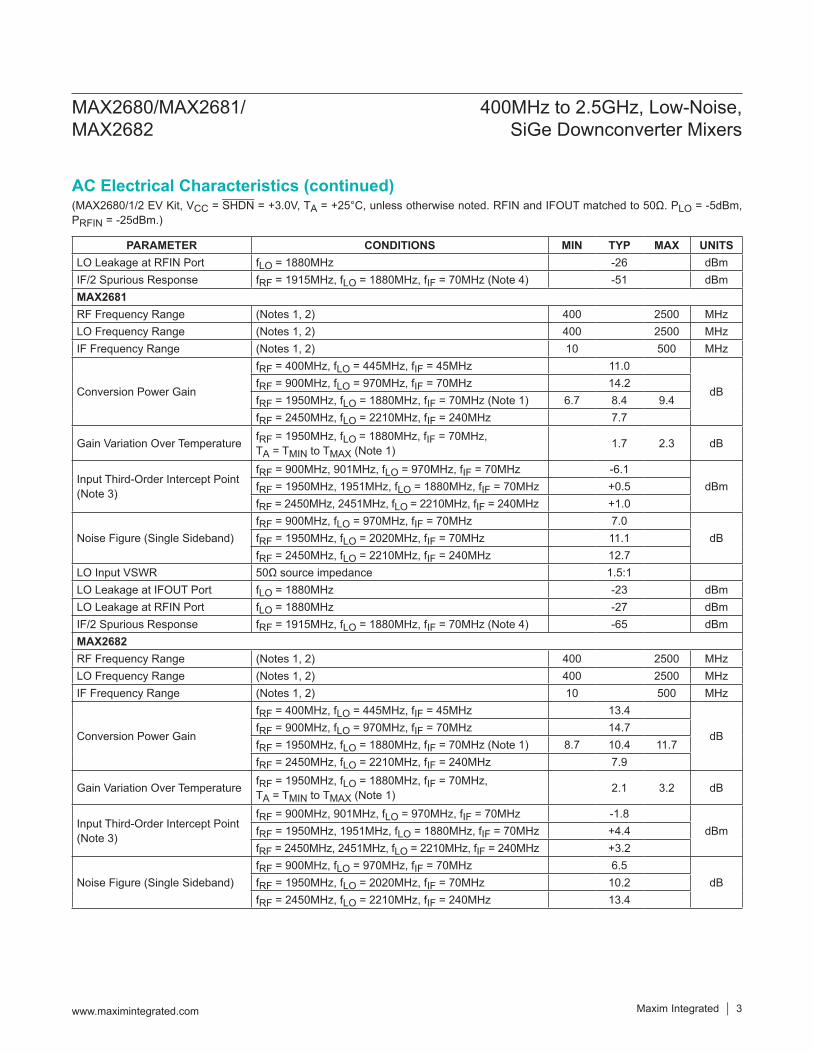
PARAMETER CONDITIONS MIN TYP MAX UNITSMAX2680RF Frequency Range (Notes 1, 2) 400 2500 MHzLO Frequency Range (Notes 1, 2) 400 2500 MHzIF Frequency Range (Notes 1, 2) 10 500 MHz
Conversion Power Gain
fRF = 400MHz, fLO = 445MHz, fIF = 45MHz 7.3
dBfRF = 900MHz, fLO = 970MHz, fIF = 70MHz 11.6fRF = 1950MHz, fLO = 1880MHz, fIF = 70MHz (Note 1) 5.7 7.6 8.6fRF = 2450MHz, fLO = 2210MHz, fIF = 240MHz 7.0
Gain Variation Over Temperature fRF = 1950MHz, fLO = 1880MHz, fIF = 70MHz, TA = TMIN to TMAX (Note 1) 1.9 2.4 dB
Input Third-Order Intercept Point (Note 3)
fRF = 900MHz, 901MHz, fLO = 970MHz, fIF = 70MHz -12.9dBmfRF = 1950MHz, 1951MHz, fLO = 1880MHz, fIF = 70MHz -8.2
fRF = 2450MHz, 2451MHz, fLO = 2210MHz, fIF = 240MHz -6.9
Noise Figure (Single Sideband)fRF = 900MHz, fLO = 970MHz, fIF = 70MHz 6.3
dBfRF = 1950MHz, fLO = 2020MHz, fIF = 70MHz 8.3fRF = 2450MHz, fLO = 2210MHz, fIF = 240MHz 11.7
LO Input VSWR 50Ω source impedance 1.5:1LO Leakage at IFOUT Port fLO = 1880MHz -22 dBm
MAX2680/MAX2681/MAX2682
400MHz to 2.5GHz, Low-Noise,SiGe Downconverter Mixers
www.maximintegrated.com Maxim Integrated 2
Absolute Maximum Ratings
Stresses beyond those listed under “Absolute Maximum Ratings” may cause permanent damage to the device. These are stress ratings only, and functional operation of the device at these or any other conditions beyond those indicated in the operational sections of the specifications is not implied. Exposure to absolute maximum rating conditions for extended periods may affect device reliability.
AC Electrical Characteristics
DC Electrical Characteristics
CAUTION! ESD SENSITIVE DEVICE
(MAX2680/1/2 EV Kit, VCC = SHDN = +3.0V, TA = +25°C, unless otherwise noted. RFIN and IFOUT matched to 50Ω. PLO = -5dBm, PRFIN = -25dBm.)
PARAMETER CONDITIONS MIN TYP MAX UNITSLO Leakage at RFIN Port fLO = 1880MHz -26 dBmIF/2 Spurious Response fRF = 1915MHz, fLO = 1880MHz, fIF = 70MHz (Note 4) -51 dBmMAX2681RF Frequency Range (Notes 1, 2) 400 2500 MHzLO Frequency Range (Notes 1, 2) 400 2500 MHzIF Frequency Range (Notes 1, 2) 10 500 MHz
Conversion Power Gain
fRF = 400MHz, fLO = 445MHz, fIF = 45MHz 11.0
dBfRF = 900MHz, fLO = 970MHz, fIF = 70MHz 14.2fRF = 1950MHz, fLO = 1880MHz, fIF = 70MHz (Note 1) 6.7 8.4 9.4fRF = 2450MHz, fLO = 2210MHz, fIF = 240MHz 7.7
Gain Variation Over Temperature fRF = 1950MHz, fLO = 1880MHz, fIF = 70MHz, TA = TMIN to TMAX (Note 1) 1.7 2.3 dB
Input Third-Order Intercept Point (Note 3)
fRF = 900MHz, 901MHz, fLO = 970MHz, fIF = 70MHz -6.1dBmfRF = 1950MHz, 1951MHz, fLO = 1880MHz, fIF = 70MHz +0.5
fRF = 2450MHz, 2451MHz, fLO = 2210MHz, fIF = 240MHz +1.0
Noise Figure (Single Sideband)fRF = 900MHz, fLO = 970MHz, fIF = 70MHz 7.0
dBfRF = 1950MHz, fLO = 2020MHz, fIF = 70MHz 11.1fRF = 2450MHz, fLO = 2210MHz, fIF = 240MHz 12.7
LO Input VSWR 50Ω source impedance 1.5:1LO Leakage at IFOUT Port fLO = 1880MHz -23 dBmLO Leakage at RFIN Port fLO = 1880MHz -27 dBmIF/2 Spurious Response fRF = 1915MHz, fLO = 1880MHz, fIF = 70MHz (Note 4) -65 dBmMAX2682RF Frequency Range (Notes 1, 2) 400 2500 MHzLO Frequency Range (Notes 1, 2) 400 2500 MHzIF Frequency Range (Notes 1, 2) 10 500 MHz
Conversion Power Gain
fRF = 400MHz, fLO = 445MHz, fIF = 45MHz 13.4
dBfRF = 900MHz, fLO = 970MHz, fIF = 70MHz 14.7fRF = 1950MHz, fLO = 1880MHz, fIF = 70MHz (Note 1) 8.7 10.4 11.7fRF = 2450MHz, fLO = 2210MHz, fIF = 240MHz 7.9
Gain Variation Over Temperature fRF = 1950MHz, fLO = 1880MHz, fIF = 70MHz, TA = TMIN to TMAX (Note 1) 2.1 3.2 dB
Input Third-Order Intercept Point (Note 3)
fRF = 900MHz, 901MHz, fLO = 970MHz, fIF = 70MHz -1.8dBmfRF = 1950MHz, 1951MHz, fLO = 1880MHz, fIF = 70MHz +4.4
fRF = 2450MHz, 2451MHz, fLO = 2210MHz, fIF = 240MHz +3.2
Noise Figure (Single Sideband)fRF = 900MHz, fLO = 970MHz, fIF = 70MHz 6.5
dBfRF = 1950MHz, fLO = 2020MHz, fIF = 70MHz 10.2fRF = 2450MHz, fLO = 2210MHz, fIF = 240MHz 13.4
MAX2680/MAX2681/MAX2682
400MHz to 2.5GHz, Low-Noise,SiGe Downconverter Mixers
www.maximintegrated.com Maxim Integrated 3
AC Electrical Characteristics (continued)
(MAX2680/1/2 EV Kit, VCC = SHDN = +3.0V, TA = +25°C, unless otherwise noted. RFIN and IFOUT matched to 50Ω. PLO = -5dBm, PRFIN = -25dBm.)
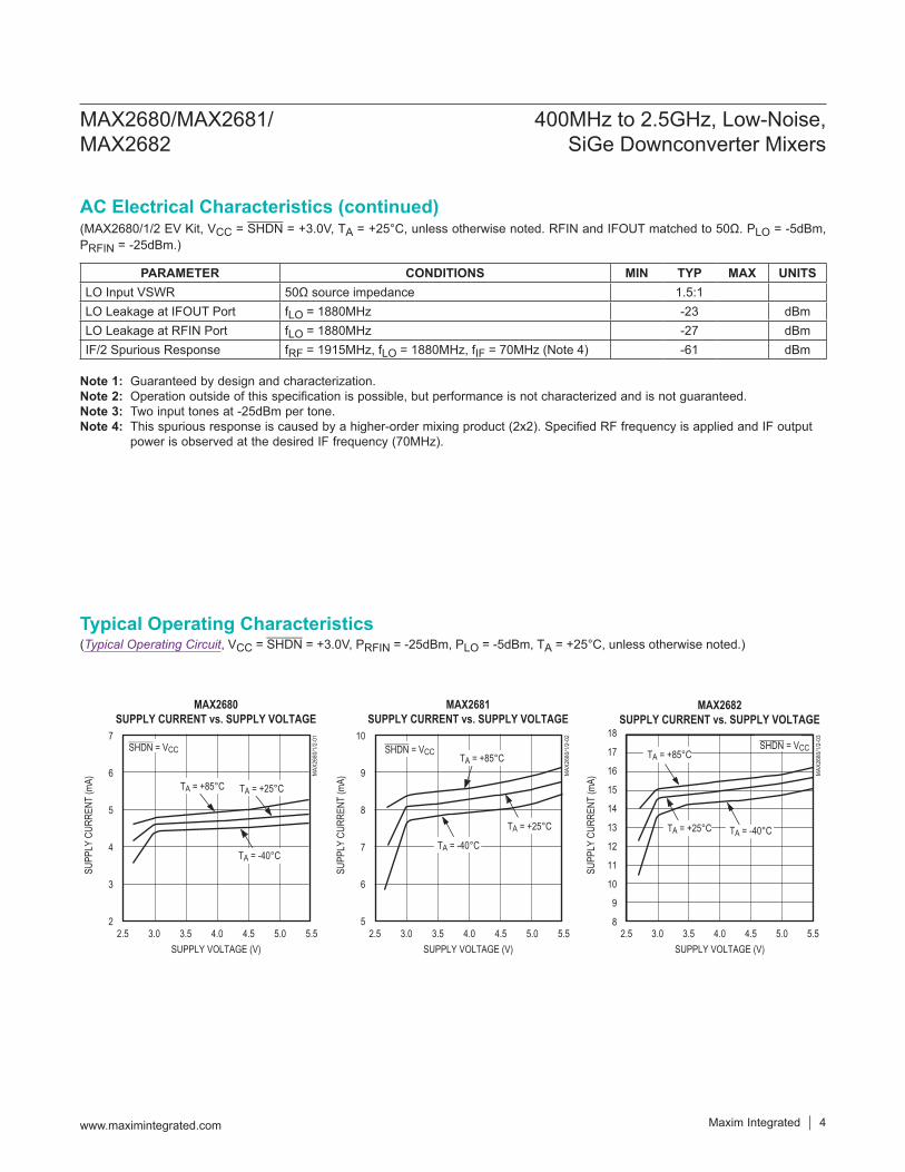
Note 1: Guaranteed by design and characterization.Note 2: Operation outside of this specification is possible, but performance is not characterized and is not guaranteed.Note 3: Two input tones at -25dBm per tone.Note 4: This spurious response is caused by a higher-order mixing product (2x2). Specified RF frequency is applied and IF output
power is observed at the desired IF frequency (70MHz).
(Typical Operating Circuit, VCC = SHDN = +3.0V, PRFIN = -25dBm, PLO = -5dBm, TA = +25°C, unless otherwise noted.)
PARAMETER CONDITIONS MIN TYP MAX UNITSLO Input VSWR 50Ω source impedance 1.5:1LO Leakage at IFOUT Port fLO = 1880MHz -23 dBmLO Leakage at RFIN Port fLO = 1880MHz -27 dBmIF/2 Spurious Response fRF = 1915MHz, fLO = 1880MHz, fIF = 70MHz (Note 4) -61 dBm
5
6
8
7
9
10
2.5 3.53.0 4.0 4.5 5.0 5.5
MAX2681SUPPLY CURRENT vs. SUPPLY VOLTAGE
MAX
2680
/1/2
-02
SUPPLY VOLTAGE (V)
SUPP
LY C
URRE
NT (m
A)
TA = +85°CSHDN = VCC
TA = +25°C
TA = -40°C
8
11
10
9
12
13
14
15
16
17
18
2.5 3.53.0 4.0 4.5 5.0 5.5
MAX2682SUPPLY CURRENT vs. SUPPLY VOLTAGE
MAX
2680
/1/2
-03
SUPPLY VOLTAGE (V)
SUPP
LY C
URRE
NT (m
A)
TA = +85°C
TA = +25°C TA = -40°C
SHDN = VCC
2
3
5
4
6
7
2.5 3.53.0 4.0 4.5 5.0 5.5
MAX2680SUPPLY CURRENT vs. SUPPLY VOLTAGE
MAX
2680
/1/2
-01
SUPPLY VOLTAGE (V)
SUPP
LY C
URRE
NT (m
A) TA = +85°C TA = +25°C
TA = -40°C
SHDN = VCC
MAX2680/MAX2681/MAX2682
400MHz to 2.5GHz, Low-Noise,SiGe Downconverter Mixers
www.maximintegrated.com Maxim Integrated 4
AC Electrical Characteristics (continued)
Typical Operating Characteristics
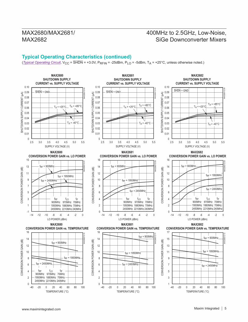
(Typical Operating Circuit, VCC = SHDN = +3.0V, PRFIN = -25dBm, PLO = -5dBm, TA = +25°C, unless otherwise noted.)
-1
5
3
1
7
9
11
13
15
-14 -10 -8-12 -6 -4 -2 0
MAX2680 CONVERSION POWER GAIN vs. LO POWER
MAX
2680
/1/2
-07
LO POWER (dBm)
CONV
ERSI
ON P
OWER
GAI
N (d
B)
fRF900MHz
1950MHz2450MHz
fLO970MHz1880MHz2210MHz
fIF70MHz70MHz240MHz
fRF = 900MHz
fRF = 2450MHzfRF = 1950MHz
0
6
4
2
8
10
12
14
16
-14 -10 -8-12 -6 -4 -2 0
MAX2681 CONVERSION POWER GAIN vs. LO POWER
MAX
2680
/1/2
-08
LO POWER (dBm)
CONV
ERSI
ON P
OWER
GAI
N (d
B)
fRF = 900MHz
fRF = 1950MHz
fRF = 2450MHz
fRF900MHz
1950MHz2450MHz
fLO970MHz
1880MHz2210MHz
fIF70MHz70MHz
240MHz0
6
4
2
8
10
12
14
16
-14 -10 -8-12 -6 -4 -2 0
MAX2682 CONVERSION POWER GAIN vs. LO POWER
MAX
2680
/1/2
-09
LO POWER (dBm)
CONV
ERSI
ON P
OWER
GAI
N (d
B)fRF = 900MHz
fRF = 1950MHz
fRF = 2450MHz
fRF900MHz
1950MHz2450MHz
fLO970MHz
1880MHz2210MHz
fIF70MHz70MHz240MHz
0
6
4
2
8
10
12
14
16
-40 0 20-20 40 60 80 100
MAX2680 CONVERSION POWER GAIN vs. TEMPERATURE
MAX
2680
/1/2
-10
TEMPERATURE (°C)
CONV
ERSI
ON P
OWER
GAI
N (d
B)
fRF = 900MHz
fRF = 1950MHz
fRF = 2450MHz
fRF900MHz
1950MHz2450MHz
fLO970MHz
1880MHz2210MHz
fIF70MHz70MHz240MHz
0
6
4
2
8
10
12
14
16
-40 0 20-20 40 60 10080
MAX2681 CONVERSION POWER GAIN vs. TEMPERATURE
MAX
2680
/1/2
-11
TEMPERATURE (°C)
CONV
ERSI
ON P
OWER
GAI
N (d
B)
fRF = 900MHz
fRF = 1950MHz
fRF = 2450MHz
1
7
5
3
9
11
13
15
17
-40 0 20-20 40 60 80 100
MAX2682 CONVERSION POWER GAIN vs. TEMPERATURE
MAX
2680
/1/2
-12
TEMPERATURE (°C)
CONV
ERSI
ON P
OWER
GAI
N (d
B)
fRF = 900MHz
fRF = 1950MHz
fRF = 2450MHz
0
0.03
0.02
0.01
0.04
0.05
0.06
0.07
0.08
0.09
0.10
2.5 3.53.0 4.0 4.5 5.0 5.5
MAX2680SHUTDOWN SUPPLY
CURRENT vs. SUPPLY VOLTAGEM
AX26
80/1
/2-0
4
SUPPLY VOLTAGE (V)
SHUT
DOW
N SU
PPLY
CUR
RENT
(µA)
TA = +85°CTA = +25°C
TA = -40°C
SHDN = GND
0
0.03
0.02
0.01
0.04
0.05
0.06
0.07
0.08
0.09
0.10
2.5 3.53.0 4.0 4.5 5.0 5.5
MAX2681SHUTDOWN SUPPLY
CURRENT vs. SUPPLY VOLTAGE
MAX
2680
/1/2
-05
SUPPLY VOLTAGE (V)
SHUT
DOW
N SU
PPLY
CUR
RENT
(µA)
TA = +85°CTA = +25°C
TA = -40°C
SHDN = GND
0
0.03
0.02
0.01
0.04
0.05
0.06
0.07
0.08
0.09
0.10
2.5 3.53.0 4.0 4.5 5.0 5.5
MAX2682SHUTDOWN SUPPLY
CURRENT vs. SUPPLY VOLTAGE
MAX
2680
/1/2
-06
SUPPLY VOLTAGE (V)
SHUT
DOW
N SU
PPLY
CUR
RENT
(µA)
TA = +85°CTA = +25°C
TA = -40°C
SHDN = GND
MAX2680/MAX2681/MAX2682
400MHz to 2.5GHz, Low-Noise,SiGe Downconverter Mixers
Maxim Integrated 5www.maximintegrated.com
Typical Operating Characteristics (continued)
(Typical Operating Circuit, VCC = SHDN = +3.0V, PRFIN = -25dBm, PLO = -5dBm, TA = +25°C, unless otherwise noted.)
-10
-8
-9
-7
-6
-5
-14 -10 -8-12 -6 -4 -2 0
MAX2680 INPUT IP3 vs. LO POWER
MAX
2680
/1/2
-13
LO POWER (dBm)
INPU
T IP
3 (dB
m)
fRF = 1950MHz, 1951MHzfLO = 1880MHzfIF = 70MHzPRFIN = -25dBm PER TONE
-3
-1
-2
0
1
2
-14 -10 -8-12 -6 -4 -2 0
MAX2681 INPUT IP3 vs. LO POWER
MAX
2680
/1/2
-14
LO POWER (dBm)
INPU
T IP
3 (dB
m)
fRF = 1950MHz, 1951MHzfLO = 1880MHzfIF = 70MHzPRFIN = -25dBm PER TONE
0
3
2
4
1
5
6
7
-14 -10 -8-12 -6 -4 -2 0
MAX2682INPUT IP3 vs. LO POWER
MAX
2680
/1/2
-15
LO POWER (dBm)
INPU
T IP
3 (dB
m)
fRF = 1950MHz, 1951MHzfLO = 1880MHzfIF = 70MHzPRFIN = -25dBm PER TONE
0
6
4
10
8
2
12
14
16
-14 -10 -8-12 -6 -4 -2 0
MAX2680NOISE FIGURE vs. LO POWER
MAX
2680
/1/2
-16
LO POWER (dBm)
NOIS
E FI
GURE
(dB)
fRF = 900MHz
fRF = 1950MHz
fRF = 2450MHz
fRF900MHz
1950MHz2450MHz
fLO970MHz2020MHz2210MHz
fIF70MHz70MHz70MHz
0
8
6
14
12
10
2
4
16
18
20
-14 -10 -8-12 -6 -4 -2 0
MAX2681NOISE FIGURE vs. LO POWER
MAX
2680
/1/2
-17
LO POWER (dBm)
NOIS
E FI
GURE
(dB)
fRF = 900MHz
fRF = 1950MHz
fRF = 2450MHz
fRF900MHz1950MHz2450MHz
fLO970MHz
2020MHz2210MHz
fIF70MHz70MHz70MHz
0
10
5
15
20
25
-14 -10 -8-12 -6 -4 -2 0
MAX2682 NOISE FIGURE vs. LO POWER
MAX
2680
/1/2
-18
LO POWER (dBm)
NOIS
E FI
GURE
(dB)
fRF = 900MHz
fRF = 1950MHz
fRF = 2450MHz
fRF900MHz
1950MHz2450MHz
fLO970MHz
2020MHz2210MHz
fIF70MHz70MHz70MHz
0
150
100
50
200
250
300
0 1000500 1500 2000 2500
MAX2680 RF PORT IMPEDANCE vs. RF FREQUENCY
MAX2680/1/2-19
RF FREQUENCY (MHz)
REAL
IMPE
DANC
E (Ω
)
-600
-300
-400
-500
-200
-100
0
IMAG
INAR
Y IM
PEDA
NCE
(W)
IMAGINARY
REALfLO = 970MHzPLO = -5dBm
0
150
100
50
200
250
300
0 500 1000 1500 2000 2500
MAX2681 RF PORT IMPEDANCE vs. RF FREQUENCY
MAX2680/1/2-20
RF FREQUENCY (MHz)
REAL
IMPE
DANC
E (Ω
)
IMAGINARY
REALfLO = 970MHzPLO = -5dBm
-600
-300
-400
-500
-200
-100
0
IMAG
INAR
Y IM
PEDA
NCE
(Ω)
0
150
100
50
200
250
300
0 1000500 1500 2000 2500
MAX2682 RF PORT IMPEDANCE vs. RF FREQUENCY
MAX2680/1/2-21
RF FREQUENCY (MHz)
REAL
IMPE
DANC
E (Ω
)
-600
-300
-400
-500
-200
-100
0IM
AGIN
ARY
IMPE
DANC
E (Ω
)IMAGINARY
REALfLO = 970MHzPLO = -5dBm
MAX2680/MAX2681/MAX2682
400MHz to 2.5GHz, Low-Noise,SiGe Downconverter Mixers
Maxim Integrated 6www.maximintegrated.com
Typical Operating Characteristics (continued)
(Typical Operating Circuit, VCC = SHDN = +3.0V, PRFIN = -25dBm, PLO = -5dBm, TA = +25°C, unless otherwise noted.)
0
600
400
200
800
1000
1200
0 200100 300 400 500
MAX2680 IF PORT IMPEDANCE vs. IF FREQUENCY
MAX2680/1/2-22
IF FREQUENCY (MHz)
REAL
IMPE
DANC
E (Ω
)
-600
-300
-400
-500
-200
-100
0IM
AGIN
ARY
IMPE
DANC
E (Ω
)
IMAGINARY
REAL
fLO = 970MHzPLO = -5dBm
0
600
400
200
800
1000
1200
0 200100 300 400 500
MAX2681 IF PORT IMPEDANCE vs. IF FREQUENCY
MAX2680/1/2-23
IF FREQUENCY (MHz)
REAL
IMPE
DANC
E (Ω
)
-600
-300
-400
-500
-200
-100
0
IMAG
INAR
Y IM
PEDA
NCE
(Ω)
IMAGINARY
REAL
fLO = 970MHzPLO = -5dBm
0
300
200
100
500
400
600
700
800
0 200100 300 400 500
MAX2682IF PORT IMPEDANCE vs. IF FREQUENCY
MAX2680/1/2-24
IF FREQUENCY (MHz)
REAL
IMPE
DANC
E (Ω
)
-400
-350
-250
-200
-300
-150
-50
-100
0
IMAG
INAR
Y IM
PEDA
NCE
(Ω)
IMAGINARY
REAL
fLO = 970MHzPLO = -5dBm
-40
-30
-35
-20
-25
-10
-15
-5
+5
0
+10
200 760 1320 1880 2440 3000
MAX2680LO PORT RETURN LOSS
MAX
2680
/1/2
-25
FREQUENCY (MHz)
RETU
RN LO
SS (d
B)
-40
-30
-35
-20
-25
-10
-15
-5
+5
0
+10
200 760 1320 1880 2440 3000
MAX2681LO PORT RETURN LOSS
MAX
2680
/1/2
-26
FREQUENCY (MHz)
RETU
RN LO
SS (d
B)
-40
-30
-35
-20
-25
-10
-15
-5
+5
0
+10
200 760 1320 1880 2440 3000
MAX2682LO PORT RETURN LOSS
MAX
2680
/1/2
-27
FREQUENCY (MHz)
RETU
RN LO
SS (d
B)
0
10
5
20
15
30
25
35
0 1000500 1500 2000 2500
MAX2680LO-to-IF AND LO-to-RF ISOLATION
MAX
2680
/1/2
-28
LO FREQUENCY (MHz)
ISOL
ATIO
N (d
B)
LO-to-IF ISOLATION
LO-to-RF ISOLATION
0
10
5
25
20
15
35
30
40
0 1000500 1500 2000 2500
MAX2681LO-to-IF AND LO-to-RF ISOLATION
MAX
2680
/1/2
-29
LO FREQUENCY (MHz)
ISOL
ATIO
N (d
B)
LO-to-IF ISOLATION
LO-to-RF ISOLATION
10
15
25
20
30
35
0 1000500 1500 2000 2500
MAX2682LO-to-IF AND LO-to-RF ISOLATION
MAX
2680
/1/2
-30
LO FREQUENCY (MHz)
ISOL
ATIO
N (d
B)
LO-to-IF ISOLATION
LO-to-RF ISOLATION
MAX2680/MAX2681/MAX2682
400MHz to 2.5GHz, Low-Noise,SiGe Downconverter Mixers
Maxim Integrated 7www.maximintegrated.com
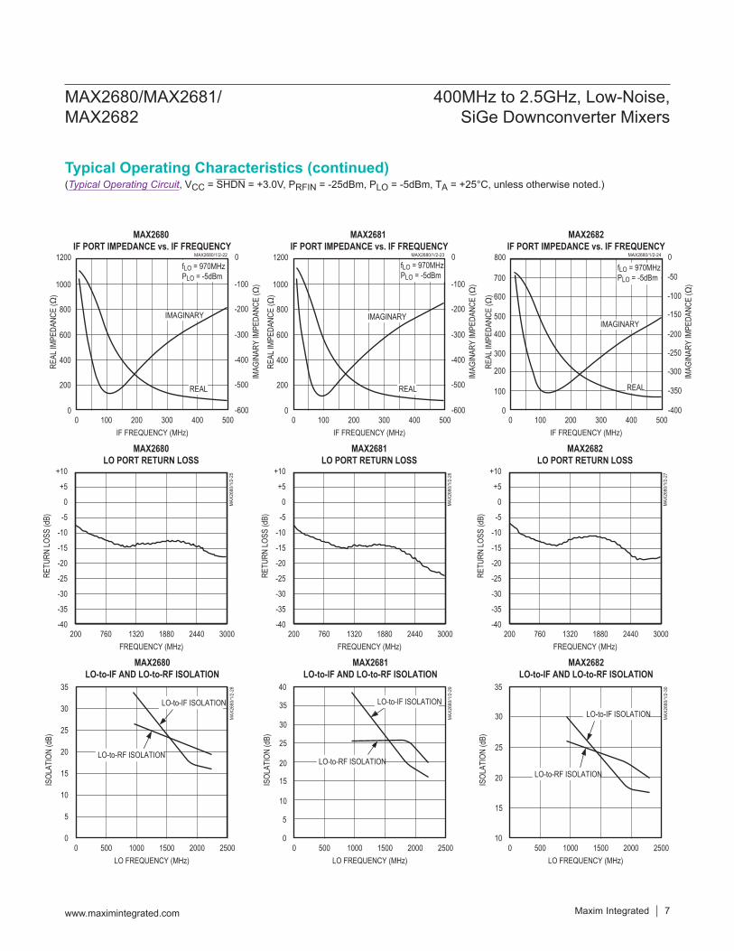
Typical Operating Characteristics (continued)
(Typical Operating Circuit, VCC = SHDN = +3.0V, PRFIN = -25dBm, PLO = -5dBm, TA = +25°C, unless otherwise noted.)
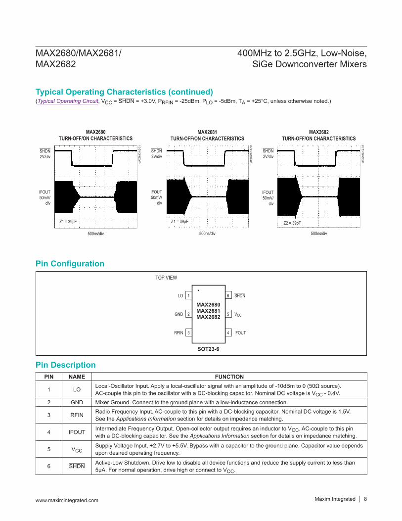
PIN NAME FUNCTION
1 LO Local-Oscillator Input. Apply a local-oscillator signal with an amplitude of -10dBm to 0 (50Ω source). AC-couple this pin to the oscillator with a DC-blocking capacitor. Nominal DC voltage is VCC - 0.4V.
2 GND Mixer Ground. Connect to the ground plane with a low-inductance connection.
3 RFIN Radio Frequency Input. AC-couple to this pin with a DC-blocking capacitor. Nominal DC voltage is 1.5V. See the Applications Information section for details on impedance matching.
4 IFOUT Intermediate Frequency Output. Open-collector output requires an inductor to VCC. AC-couple to this pin with a DC-blocking capacitor. See the Applications Information section for details on impedance matching.
5 VCCSupply Voltage Input, +2.7V to +5.5V. Bypass with a capacitor to the ground plane. Capacitor value depends upon desired operating frequency.
6 SHDN Active-Low Shutdown. Drive low to disable all device functions and reduce the supply current to less than 5μA. For normal operation, drive high or connect to VCC.
SHDN2V/div
IFOUT50mV/
div
500ns/div
MAX2680TURN-OFF/ON CHARACTERISTICS
MAX
2680
/1/2
-31
Z1 = 39pF
SHDN2V/div
IFOUT50mV/
div
500ns/div
MAX2681TURN-OFF/ON CHARACTERISTICS
MAX
2680
/1/2
-32
Z1 = 39pF
SHDN2V/div
IFOUT50mV/
div
500ns/div
MAX2682TURN-OFF/ON CHARACTERISTICS
MAX
2680
/1/2
-33
Z2 = 39pF
MAX2680/MAX2681/MAX2682
400MHz to 2.5GHz, Low-Noise,SiGe Downconverter Mixers
www.maximintegrated.com Maxim Integrated 8
Pin Description
Typical Operating Characteristics (continued)
GND
IFOUTRFIN
1 6 SHDN
5 VCC
LO
MAX2680MAX2681MAX2682
SOT23-6
TOP VIEW
2
3 4
Pin Configuration
Detailed DescriptionThe MAX2680/MAX2681/MAX2682 are 400MHz to 2.5GHz, silicon-germanium, double-balanced downcon-verter mixers. They are designed to provide optimum linearity performance for a specified supply current. They consist of a double-balanced Gilbert-cell mixer with single-ended RF, LO, and IF port connections. An on-chip bias cell provides a low-power shutdown feature. Consult the Selector Guide for device features and comparison.
Applications InformationLocal-Oscillator (LO) InputThe LO input is a single-ended broadband port with a typical input VSWR of better than 2.0:1 from 400MHz to 2.5GHz. The LO signal is mixed with the RF input sig-nal, and the resulting downconverted output appears at IFOUT. AC-couple LO with a capacitor. Drive the LO port with a signal ranging from -10dBm to 0 (50Ω source).
RF InputThe RF input frequency range is 400MHz to 2.5GHz. The RF input requires an impedance-matching network as well as a DC-blocking capacitor that can be part of the matching network. Consult Tables 1 and 2, as well as the RF Port Impedance vs. RF Frequency graph in the Typical Operating Characteristics section for information on matching.
IF OutputThe IF output frequency range extends from 10MHz to 500MHz. IFOUT is a high-impedance, open-collector output that requires an external inductor to VCC for proper biasing. For optimum performance, the IF port requires an imped-ance-matching network. The configuration and values for the matching network is dependent upon the frequency and desired output impedance. For assistance in choosing com-ponents for optimal performance, see Table 3 and Table 4 as well as the IF Port Impedance vs. IF Frequency graph in the Typical Operating Characteristics section.
Power-Supply and SHDN BypassingProper attention to voltage supply bypassing is essential for high-frequency RF circuit stability. Bypass VCC with a 10μF capacitor in parallel with a 1000pF capacitor. Use separate vias to the ground plane for each of the bypass capacitors and minimize trace length to reduce induc-tance. Use separate vias to the ground plane for each ground pin. Use low-inductance ground connections.Decouple SHDN with a 1000pF capacitor to ground to minimize noise on the internal bias cell. Use a series resistor (typically 100Ω) to reduce coupling of high-fre-quency signals into the SHDN pin.
Layout IssuesA well-designed PC board is an essential part of an RF circuit. For best performance, pay attention to power-supply issues as well as to the layout of the RFIN and IFOUT impedance-matching network.
Table 1. RFIN Port Impedance
Table 2. RF Input Impedance-Matching Component Values
Note: Z1, Z2, and Z3 are found in the Typical Operating Circuit.
PARTFREQUENCY
400MHz 900MHz 1950MHz 2450MHzMAX2680 179-j356 54-j179 32-j94 33-j73
MAX2681 209-j332 75-j188 34-j108 33-j86
MAX2682 206-j306 78-j182 34-j106 29-j86
MATCHINGCOMPONENTS
FREQUENCYMAX2680 MAX2681 MAX2682
400MHz
900MHz
1950MHz
2450MHz
400MHz
900MHz
1950MHz
2450MHz
400MHz
900MHz
1950MHz
2450MHz
Z1 86nH 270pF 1.5pF Short 68nH 270pF 1.5pF Short 68nH 1.5pF Short ShortZ2 270pF 22nH 270pF 270pF 270pF 18nH 270pF 270pF 270pF 270pF 270pF 270pFZ3 Open Open 1.8nH 1.8nH 0.5pF Open 1.8nH 2.2nH 0.5pF 10nH 2.2nH 1.2nH
MAX2680/MAX2681/MAX2682
400MHz to 2.5GHz, Low-Noise,SiGe Downconverter Mixers
www.maximintegrated.com Maxim Integrated 9
Power-Supply LayoutTo minimize coupling between different sections of the IC, the ideal power-supply layout is a star configuration with a large decoupling capacitor at a central VCC node. The VCC traces branch out from this central node, each going to a separate VCC node on the PC board. At the end of each trace is a bypass capacitor that has low ESR at the RF frequency of operation. This arrangement provides local decoupling at the VCC pin. At high frequencies, any signal leaking out of one supply pin sees a relatively high impedance (formed by the VCC trace inductance) to the central VCC node, and an even higher impedance to any other supply pin, as well as a low impedance to ground through the bypass capacitor.
Impedance-Matching Network LayoutThe RFIN and IFOUT impedance-matching networks are very sensitive to layout-related parasitics. To mini-mize parasitic inductance, keep all traces short and place components as close as possible to the chip. To minimize parasitic capacitance, use cutouts in the ground plane (and any other plane) below the matching network components. However, avoid cutouts that are larger than necessary since they act as aperture antennas.
Table 3. IFOUT Port Impedance
Table 4. IF Output Impedance-Matching Components
PARTFREQUENCY
45MHz 70MHz 240MHzMAX2680 960-j372 803-j785 186-j397
MAX2681 934-j373 746-j526 161-j375
MAX2682 670-j216 578-j299 175-j296
MATCHINGCOMPONENT
FREQUENCY45MHz 70MHz 240MHz
L1 390nH 330nH 82nH
C2 39pF 15pF 3pF
R1 250Ω Open Open
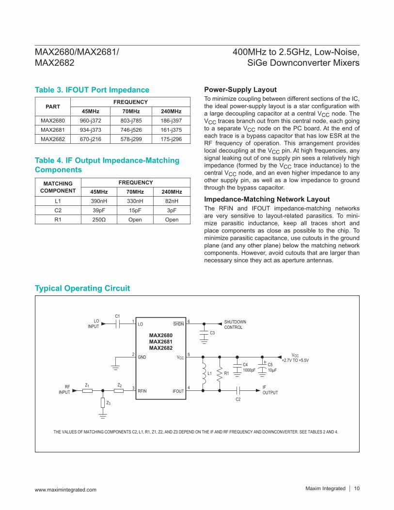
MAX2680MAX2681MAX2682
LO
C3
6
5
4
SHUTDOWNCONTROL
1 SHDN
VCC
RFINPUT
LOINPUT
C1
IFOUT
2
Z2
Z3
Z1 3
GND
RFIN
THE VALUES OF MATCHING COMPONENTS C2, L1, R1, Z1, Z2, AND Z3 DEPEND ON THE IF AND RF FREQUENCY AND DOWNCONVERTER. SEE TABLES 2 AND 4.
VCC+2.7V TO +5.5V
IF OUTPUT
L1
C2
R1
C41000pF
C510µF
MAX2680/MAX2681/MAX2682
400MHz to 2.5GHz, Low-Noise,SiGe Downconverter Mixers
www.maximintegrated.com Maxim Integrated 10
Typical Operating Circuit
MAX2680/MAX2681/MAX2682
400MHz to 2.5GHz, Low-Noise,SiGe Downconverter Mixers
www.maximintegrated.com Maxim Integrated 11
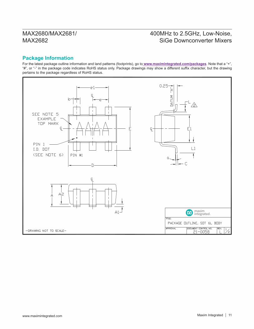
Package InformationFor the latest package outline information and land patterns (footprints), go to www.maximintegrated.com/packages. Note that a “+”, “#”, or “-” in the package code indicates RoHS status only. Package drawings may show a different suffix character, but the drawing pertains to the package regardless of RoHS status.
Maxim Integrated cannot assume responsibility for use of any circuitry other than circuitry entirely embodied in a Maxim Integrated product. No circuit patent licenses are implied. Maxim Integrated reserves the right to change the circuitry and specifications without notice at any time. The parametric values (min and max limits) shown in the Electrical Characteristics table are guaranteed. Other parametric values quoted in this data sheet are provided for guidance.
Maxim Integrated and the Maxim Integrated logo are trademarks of Maxim Integrated Products, Inc.
MAX2680/MAX2681/MAX2682
400MHz to 2.5GHz, Low-Noise,SiGe Downconverter Mixers
© 2003 Maxim Integrated Products, Inc. 12
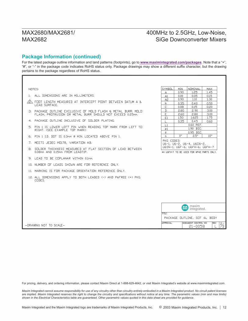
Package Information (continued)For the latest package outline information and land patterns (footprints), go to www.maximintegrated.com/packages. Note that a “+”, “#”, or “-” in the package code indicates RoHS status only. Package drawings may show a different suffix character, but the drawing pertains to the package regardless of RoHS status.
For pricing, delivery, and ordering information, please contact Maxim Direct at 1-888-629-4642, or visit Maxim Integrated’s website at www.maximintegrated.com.