Embed Size (px)
Citation preview

KU-BAND MINIATURE MODULATORS
Robert L. ErnstRCA I Government Communications SystemsAdvanced Communications Laboratory '
CNOSomerville, New Jersey 08876
March 1973Final Report for Period 1 January 1972-15 February 1973
Prepared for
GODDARD SPACE FLIGHT CENTERGreenbelt, Maryland 20771
(NASA-CR -1 2 3 O) - KU-BAND MINIATURE -- N73-2?78MODULATORS Final Report, 1 Jan. 1972g-15 Feb. 1973 (Radio Corp. of America)
145 p Ric $4.25 23 .o CSCL 17B UnclasG3/07 02523
https://ntrs.nasa.gov/search.jsp?R=19730013351 2018-07-13T06:44:48+00:00Z

TECHNICAL REPORT STANDARD TITLE PAGEI. Report No. 2. Government Accession No.I 3. Recipient's Catalog No.
4. Title and Subtitle 5. Report Dote
Ku-Band Miniature Modulators March 19736. Performing Organization Code
7. Author(s) 8. Performing Organization Report No.Robert L. Ernst
9. Performing Organization Name and Address 10. Work Unit No.
RCA/Government Communications Systems11. Contract or Grant No.Advanced Communications Laboratory . Contrat or Grnt No.
NAS 5-23050Somerville, New Jersey 0887613. Type of Report and Period Covered
12. Sponsoring Agency Name and Address Final ReportGoddard Space Flight Center 1 January 1972-Greenbelt, Maryland 20771 15 February 1973
14. Sponsoring Agency Code
Technical Monitor: Wayne Hughes15. Supplementary Notes
16. Abstract
Ku-Band Microminiature Modulators have been designed to convert a 10 mW signalat 400 MHz to a 10 mW signal at 15 GHz. The designs incorporate gallium arsenideSchottky barrier varactors used in upper-sideband up-converters and include the useof Ku-Band microstrip circulators and hairpin resonator bandpass filters at 2.1 GHzand 2.5 GHz. The evaluation compares the design and fabrication of a single up-conversion unit with a double up-conversion unit. Various filter configurations arestudies, and the use of both alumina and quartz substrates are considered. Thevarious impedance matching networks are evaluated using computer aided designtechniques.
The output of a double conversion unit fabricated on alumina substrates is about+3.4 dBm, while the output of a single-conversion unit fabricated on a quartzsubstrate is about +8. 5 dBm. Recommendations for the selection of frequenciesand the choice of substrates for optimum up-converter performance are given.
17. Key Words (Selected by Author(s)) 18. Distribution StatementHairpin ResonatorKu-Band Microminiature ModulatorMIC (Microwave Integrated Circuit)Microcircuit CirculatorQuartz Substrates
19. Security Classif. (of this report) 20. Security Classif. (of this page) 21. No. of Pages 22. Price*
Unclassified Unclassified
t
I
I
I

PRECEDING PAGE BLANK NOT FILMED
PRE FACE
The objective of this program is the design, development, and fabrication of five modelsof a Ku-Band Microminiature Modulator which converts a signal at 400 MHZ to a signalat 15 GHZ using state-of-the-art microwave integrated circuit (MIC) techniques. Atwo-stage up-converter requiring pumps at 2.190 GHZ and 12.410 GHZ was developedfirst in conformance with the original goals. Power output and bandwidth performancewere low. Based upon the technology learned during the design phase of this unit, anew design utilizing a single pump at 14.6 GHZ and having one-fifth the size and weightof the two stage unit was proposed. This unit was then developed and fabricated, andproduced 5 dB greater output and much greater bandwidth than the original two-stageunit. The delivered units consisted of two two-stage units having a midband output ofabout +3.4 dBm and three single-stage units having an output of +8.5 dBm.
It is recommended that upper sideband up-converters having an output at Ku-band fre-quencies utilize 10 mil thick quartz substrates. A high ratio of output-to-input fre-quencies is very desirable to simplify circuit design and layout.
Preceding page blank
iii/iv

TABLE OF CONTENTS
Page
1-1
Section
1 INTRODUCTION ...................................
2 VARACTOR DIODE SELECTION AND CHARACTERIZATION . . . . . 2-12.1 Diode Parameter Selection ............2.2 Predicted Circuit Performance . . . .2.3 Up-Converter Optimizations ......
2.3.1 Maximum Pump Efficiency . .2.3.2 Maximum Total Efficiency . .2.3.3 Maximum Output Power ....
2.4 Comparison of Optimizations . ....2.5 Diode Package Transformation.....
3 .DESIGN OF AUXILIARY CIRCUITS ....... .3.1 Filter Designs . . . . ..................
3.1.1 2.1 GHz and 2.5 GHz Bandpass Filters
3.23.1.2 Ku-Band Filters .............. Ku-Band Circulators ................
............ 2-1
............ 2-3
............ 2-3.........- . 2-3
............ 2-4
............ 0 2-5
............ 002-5
............ 002-8
............ 3-1............ 3-13-1
3-1............ ** 3-6............ 3-6
4 UP-CONVERTER CIRCUIT DESIGNS . .............4.1 Early Two-Stage Designs ..... ..... ....... .... *..
4.2 Final Two-Stage Designs .... ......... ............4.3 Frequency Selection Criteria .......................4.4 Single Stage Design ................ .. ........... .
5 MEASURED PERFORMANCE .........
6 NEW TECHNOLOGY.................................
7 CONCLUSIONS AND RECOMMENDATIONS. .................
APPENDIX
REFERENCES. ................................... 0
4-14-14-64-104-11
5-1
6-1
7-1
A-1
V
* . .. .
* . . . .
* . . . .
* . .. .
*0 8 0 0 0

LIST OF ILLUSTRATIONS
Figure Page
2-1 Equivalent Circuit of a Packaged Varactor Diode ...... ........ 2-8
3-1 Tapped Bandpass Filter Configuration. .......... i........r. 3-23-2 Performance of Tapped 2.5 GHz Bandpass Filter ............. 3-3
3-3 Hairpin Resonator Bandpass Filter Configuration ............. 3-4
3-4 Performance of Hairpin Resonator 2.5 GHz Bandpass Filter ...... 3-5
3-5 Directional Filter Configuration ......................... 3-63-6 Performance of 2.1 GHz Directional Filter ..... ............. 3-73-7 Edge Coupled Bandpass Filter Configuration .................i 3-8
3-8 Ferrite Circulator Performance ........................ 3-94-1 Layout of First Low Frequency Up-Converter ................ 4-24-2 Illustration of Impedance Terminology ....... ...... .... ... 4-3
4-3 Layout of First High Frequency Up-Converter ............. ... 4-3
4-4 Layout of Final Low Frequency Up-Converter ................ 4-74-5 Layout of Final High Frequency Up-Converter ..... .......... 4-9
4-6 Layout of Single Stage Ku-Band Modulator .................. 4-125-1 Two-Stage Ku-Band Microminiature Modulator ............... 5-15-2 Single Stage Ku-Band Microminiature Modulator .............. 5-4
7-1 Output Power Performance of Five Ku-Band MicrominiatureModulators ... ....................................... 7-1
LIST OF TABLES
Table Page
2-1 Varactor Diode Parameters ............................ 2-5
2-2 Comparison of First Up-Converter Optimizations ............. 2-6
2-3 Comparison of Second Up-Converter Optimizations ............ 2-7
2-4 Packaged Diode Impedances for the First Up-Converter ......... 2-9
2-5 Packaged Diode Impedances for the Second Up-Converter ........ 2-9
4-1 Computed Matching Network Performance for First LowFrequency Up-Converter Design......................... 4-4
4-2 Computed Matching Network Performance for First HighFrequency Up-Converter Design ......................... 4-5
4-3 Impedance Transformations in the Final Low FrequencyUp-Converter .................... 4-8
4-4 Impedance Transformations in the Final High FrequencyUp-Converter ...................... .. ............. 4-10
5-1 Power Output as a Function of Input Frequency for the FiveDelivered Modulators.......... ................... 5-3
vi

Section 1
INTRODUCTION
The object of this program is the development of five units of a Ku-Band MicrominiatureModulator. The original specifications called for the following items:
a. Upper sideband up-converter, complete with low-pass input filter and bandpassoutput filter, and capable of converting a 400 MHz ±50 MHz IF signal to a2, 500 MHz ±50 MHz signal with a minimum loss in the conversion process.Carrier and image signals will be suppressed to at least 30 dB below the2, 500 MHz ±50 MHz signal. The up-converter will operate with the followingpower levels:
10 milliwatts input power at 400 MHz ±50 MHz.
50 milliwatts input power at 2,100 MHz.
10 milliwatts output power at 2,500 MHz ±50 MHz.
b. Upper sideband up-converter, complete with low-pass input filter and band-pass output filter, and capable of converting the 2,500 MHz 450 MHz signalfrom the first converter to a signal at a frequency of 15,000 MHz +50 MHz.This second up-converter will operate with the following power levels:
10 milliwatts input power at 2,500 MHz +50 MHz.
50 milliwatts input power at 12,500 MHz.
10 milliwatts output power at 15, 000 MHz ±50 MHz.
c. -Microcircuit circulator operating at a center frequency of 12,500 MHz withsufficient bandwidth, extremely low insertion loss (;t0.25 dB) and a powerhandling capability well over the required 50 milliwatts.
d. Microcircuit circulator operating at a center frequency of 15, 000 MHz withsufficient bandwidth, extremely low insertion loss (W0.25 dB) and a powerhandling capability well over the required 100 milliwatts.
All above four elements of the modulator will be mounted within a single rectangularcontainer whose maximum outside dimensions are 1 inch x 1.5 inch x 2 inches. OSMtype coaxial fittings will be used for all input and output connections.
Both upper sideband up-converters will be constructed using gallium arsenide Schottkybarrier type diodes. All elements will be of the microminiature type construction onsapphire substrate material.
1-1

These modules required the development of filters utilizing hairpin resonators toachieve the most efficient utilization of substrate area. At 2.5 GHz, the followingperformance of a two-section filter has been achieved:
Midband Insertion Loss: 1 dB
Midband VSWR: 1.2
0.5 dB bandwidth: 100 MHz
Rejection at 2.1 GHz: 27 dB
Area Required: 450 mils x 240 mils
All garnet microstrip circulators at Ku-band were developed. Over the band of 10.5to 18 GHz, the insertion loss is less than 1 dB and the isolation greater than 12 dB.The substrate is 255 mils in diameter and 25 mils thick.
Designing a two stage up-converter as specified resulted in a circuit which is verycomplicated and critical. After tuning, an output of +3.4 dBM and a 3 dB bandwidth ofabout 100 MHz was achieved.
A new design was developed utilizing a single-stage up-converter fabricated on. a 1 inchby ½ inch quartz substrate. This design achieved an output of +8.5 dBM and had a 1 dBbandwidth of greater than 200 MHz. This circuit required little tuning, was simple,and not critical.
1-2

Section 2
VARACTOR DIODE SELECTION AND CHARACTERIZATION
The parameters of the varactor diodes chosen for the two frequency converters mustpermit operation at high efficiency for the power levels and frequencies involved. Oncethe diodes have been selected, they must be properly characterized to determine theoperating impedances. This information is then used to design the up-convertercircuits.
2.1 DIODE PARAMETER SELECTION
To satisify the requirements of the parametric up-converters, the diodes must bechosen according to the following criteria:
a. The diode must have low loss. A suitable measure of diode loss is the cut-offfrequency, fc. At any given voltage, V, the cut-off frequency is related to thediode series resistance, Rs, and junction capacitance, Cj, by the expression
1fc = 27r R C (1)
sJ]
Many diode manufacturers have standardized upon a bias of 6 volts in specifyingcut-off frequency. If the cut-off frequency is high relative to the operating fre-quencies, low loss is expected. Equation 1 shows that this quantity is raisedby decreasing R s and Cj.
b. The diode must present reasonable impedances to the circuit to facilitatematching, especially if broad bandwidth is required. Since input and outputimpedance levels of MIC's are typically 50 ohms, it is perferred to have thediode present real and reactive impedances in the range of 5 ohms to 500ohms. Using the subscripts s, p, and u to respectively denote the signal,pump, and upper sideband frequencies, the input and load resistances whichshould be presented to the varactor are given by (Ref. 1):
R. = R +R fc/f s) m/m\ (2)in s s s p u ss
In s muA
RU =-R 5 +R 5 (c/u) (MS MP/mu)
2-1

The terms ms, mp, and mu are the diode modulation ratios, and are a mea-sure of the capacitance swing resulting from the various voltage components.These expressions show that Rs and fc must be properly chosen to producerealistic impedance levels.
The reactance of the diode is given by the familiar relation:
X = 1/2irfn Cj (5)n
where the subscript n can be either s, p, or u. This shows that selecting toolow a capacitance level.can result in too great a reactance, especially at thelowest frequency, fs.
c. The diode must have sufficient power handling capability. This capability isproportional to the term
(0 + VB) 2P - (6)norm Rs
where Pnorm is called the normalization power, * is the diode contact poten-tial, and VB is the diode breakdown voltage. In an up-converter, the powerssupplied to the diode, P and Pp, and the power delivered to the output, Pu,are given by:
P = 8P c m m m +m (7)~~~~~~~ss norm\fc/ \s s p u s}
p~~ 2P = 8 I In 2m (8)p normfc \f s p u p/
m
s
_
P =8P m m m - m 2\ (9)u norm fcu s p u
It can be seen that power handling capability for a given R s is proportional tothe square of the breakdown voltage (assume 0 << VB). Hence greater powercan be handled in a diode with greater breadown voltage.
2-2

The selection of the diode parameters Rs, Cj, and VB cannot be arbitrarilymade since all three parameters are dependent upon the diode doping- density.In general, as the doping density is increased, Rs decreases, Cj increases,and VB decreases. Therefore, the choice of any diode must be based uponits predicted performance in an upconverter circuit.
2.2 PREDICTED CIRCUIT PERFORMANCE
The proper selection of a varactor diode is verified by checking its predicted circuitperformance. This means that once a diode having a specified Rs, Cj, and VB arechosen, the predicted values for the impedances and power levels based upon theequations given above, must be checked for reasonable circuit performance.
Circuit performance is also determined by the chosen values of the diode modulationratios, ms, mp, and mu. These must be selected to give optimum values for powerlevels, and overall efficiency. The three ratios are limited by the approximation:
In m + m + m < 0.25 (10)s p u
For a given selected set of values for the modulation ratios, the impedances presentedto the diode are determined from Equations 2, 3, 4, and 5.
2.3 UP-CONVERTER OPTIMIZATIONS
The up-converter can be optimized by selecting the values of ms, mp, and mu
properly. For example, the up-converter can be optimized for: a. maximum pumpefficiency; b. maximum total efficiency; or c. maximum power output. These condi-tions will now be considered separately.
2.3.1 Maximum Pump Efficiency
Maximum pump efficiency is achieved by maximizing the ratio:P
p Pp
Mathematically, the solution for this case becomes the trivial condition
m = 0.25, m = 0; m = 0. (12)s p u
2-3

Physically this means that the diode is being pumped by the signal, and that thepump and output levels are now small signals. The pump efficiency for this caseis given by:
m f 2scf
1(f(13)
m2 f 2 2s c
f fpu ,
Total efficiency, pump power, and output power are all essentially zero for this case.
2.3.2 Maximum Total Efficiency
Maximum total efficiency is achieved by maximizing the ratio:
PU
nt -= nt P + Ps p
(14)
A condition which approximates this goal is given by (Ref 2)
2w m
s s
2= w m
P P
2= w m
u u(15)
Combining this with Equation 10 results in the following expressions:
0.25m
s
1 + 21 +
(16)
+f59
f =sIn= mn
p s fp
Ofm = m
u s fu
(17)
(18)
np
2-4

2.3.3 Maximum Output Power
The values for the modulation ratios which maximize the output power, given byEquation 9, are given by the expressions:
1m =
mp
mu
f2f2 u3 f
C
·+9f
1576
(19)
(20)= ms
2m
= ' sm
1+ 2 f
u
fc
(21)
2.4 COMPARISON OF OPTIMIZATIONS
These various optimizations have been programmed on a time-shared computer tofacilitate comparison. Commercially available Gallium arsenide Schottky barrierdiodes have been selected to provide input parameters for the various calculations.The parameters of the selected diodes are summarized in Table 2-1.
Table 2-1. Varactor Diode Parameters
The predicted performances for the various optimizations are shown in Table 2-2 forthe first up-converter and in Table 2-3 for the second up-converter.
2-5
Application: First Up-converter Second Up-converter
Manufacturer: Parametric Industries Parametric Industries
Model No.: PF 4500 C PF 4500 G
Cut-off Frequency (-6V): 300 GHz 500 GHz
C (-6V): 0.2 - 0.45 pF 0.3 - 0.45 pF
Breakdown Voltage: -6 V -6 V

Table 2-2. Comparison of First Up-Converter Optimizations
(Diode: Parametric Industries PF 4500C)
Optimization I Max. Pump Eff. I Max. Total Eff. I Max. Power Out.
InS
mpP
mu
Gain (Pu/Ps)
Pump Eff.
Total Eff.
Signal Power
Pump Power
Output POwer
R.in
s
R.in
P
Ru
0.250
0
0
0
112.0
0
0.03 mW
0
0
1.26
41.4 Q
41D4 Q
XC
S
Xcp
Xx C
U
0.136
0.059
0.055
7.47 dB
106.4%
89.4%
0.18 mW
0.93 mW
0.98 mW
23.8 Q
23.8 Q
21.3 fQ
473.7 n
0.088
0.088
0.074
7.52 dB
100.1%
85.0%
0.22 mW
1.25 mW
1.25 mW
71.4 Q
14.6 fQ
14.6 R
90.2 Q?
75.8 Q
2-6
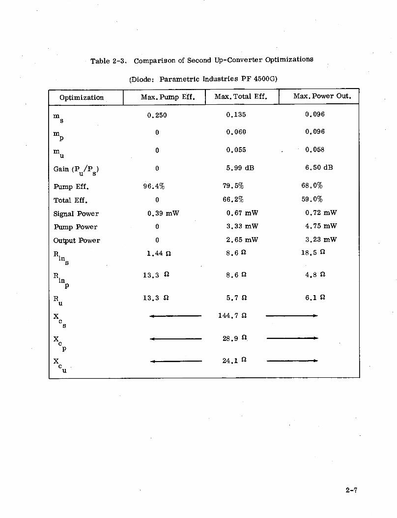
Table 2-3. Comparison of Second Up-Converter Optimizations
(Diode: Parametric Industries PF 4500G)
Optimization Max. Pump Eff. Max. Total Eff. Max. Power Out.
ms
0.250
0mp
0.135
0.060
0.096
0.096
mu
0
Gain (P /P )u s
Pump Eff.
Total Eff.
Signal Power
Pump Power
Output Power
R.in
s
R.in
p
Ru
0
96.4%
0
0.39 mW
0
0
1.44 Q
13.3 Q
13.3 Q
Xc
S
Xc
p
Xc
u
0.055
5.99 dB
79.5%
66.2%
0.67 mW
3.33 mW
2.65 mW
8.6 Q
8.6 Q
5.7 Q
0.058
6.50 dB
68.0%
59.0%
0.72 mW
4.75 mW
3.23 mW
18.5 g
4.8 2
6.1 Q
144.7 2
28.9 Q
24.1 Ql
2-7
I

In comparing data in Tables 2-2 and 2-3, it must be realized that the varactors areusually slightly overdriven and that actual power levels can be as much as ten timesgreater than the levels indicated. These tables show clearly that the solution ofmaximum pump efficiency is not practical. The other two solutions are comparable.The maximum power out condition is used for the designs in this program. Thiscondition results in greatest output power with a small loss in total efficiency andmore practical resistance levels.
2.5 DIODE PACKAGE TRANSFORMATION
The impedance of the varactor diode, determined by the maximum output power optimi-zation, is modified by the package parasitic inductance and capacitance as shown inFigure 2-1. The impedances resulting from this transformation are given in Table2-4 for the first up-converter and in Table 2-5 for the second up-converter.
L
Cp-_ ~~~~Cj (v): DIODE JUNCTION CAPACITANCE_ t P~R s : DIODE SPREADING RESISTANCE
. Rs Lp : PACKAGE CONTACT INDUCTANCEC : PACKAGE STRAY CAPACITANCE
Cj.(v) P
Figure 2-1. Equivalent Circuit of a Packaged Varactor Diode
These impedance values are the ones to be used in designing the up-converter cir-cuitry. Sufficient data has been tabulated to permit the determination of input andoutput VSWR's and resulting mismatch losses across the frequency bands of interest.
2-8

Table 2-4. Packaged Diode Impedances For The First Up-Converter
(C =0.85pF, C3 -0.15pF, Lp =0.1 nH)v pp
Table 2-5. Packaged Diode Impedances For the Second Up-Converter
(C = 0.45pF, C =0.15pF, LV ~P P
= 0.1 nH)
2-9/2-10
Frequency (GHz) ZTotal (Ohms) R (Ohms)V
2.45 10.6-j 107.7 18.8
2.50 10.4-j 105.6 18.5
2.55 10.2-j 103.4 18.1
12.50 3.1-j 16.6 4.9
14.95 4.2-j 12.2 6.1
15.00 4.2-j 12.1 6.1
15.05 4.2-j 12.0 6.0

Section 3
DESIGN OF AUXILIARY CIRCUITS
Many different circuits have been designed to meet the specifications of the Ku-bandMicrominiature Modulator. The design criterion of typical circuits approach will bebriefly discussed together with a tabulation of predicted performance and a listing ofadvantages and disadvantages. The recommendations for the best way to satisfy systemspecifications will be described later.
All of the considered approaches require filter circuits and circulators. Suitable filterand circulator configurations with measured performance follow.
3.1 FILTER DESIGNS
3.1.1 2.1 GHz and 2.5 GHz Bandpass Filters
Bandpass filters normally incorporate half-wavelength coupled resonators. At 2.1 GHz,this corresponds to a length of approximately 1.1 inches. The overall filter designed inthe conventional edge-coupled straight resonator approach would be almost 1-3/4 incheslong. Because an excessive substrate area would be consumed by such a design, newfilter configurations have been tried instead (Ref. 3, 4).
One configuration uses quarter-wavelength resonators which are short circuited at oneend and open circuited at the other. Input and output lines are directly tapped into theresonators as shown in Figure 3-1. In principle, the impedance presented to the inputand output can be controlled by the location of the tap-point. Lower impedances arepresented by approaching the short circuit end, while higher impedances result as thetap is moved closer to the open-circuited end.
A filter of this type has been designed for 2.5 GHz, fabricated, and tested. The per-formance, plotted in Figure 3-2, can be summarized as follows:
Midband Insertion Loss 1. 5 dB
Midband VSWR 1.6
0.5 dB bandwidth 110 MHz
Rejection at 2.1 GHz 25 dB
Area required 455 mils x 155 mils
3-1

GROUND SHORT --_I
GROUND SHORT
4- 50-OHM TAP-OFFPOINT
Figure 3-1. Tapped Bandpass Filter Configuration
This configuration has the advantages of giving good performance in a compact area.However, reproducible results are difficult to obtain because the location of the shortcircuit through the substrate is extremely critical even at this comparatively low fre-quency. Furthermore, the quality of the short circuit has a direct effect on the inser-tion loss of the filter.
An alternate band pass filter configuration recently described in the literature is thehairpin resonator filter. This filter uses resonators bent back upon themselves at theirmidpoints and coupled along half their length as shown in Figure 3-3. Filters of thistype have been fabricated at 2.5 GHz. The performance is plotted in Figure 3-4 and issummarized as follows:
Midband Insertion Loss 1. dB
Midband VSWR
0.5 dB Bandwidth
Rejection at 2.1 GHz
1.2
100 MHz
27 dB
Area required 450 mils x 240 mils
3-2

2.2 24 2.6 .2.8 3.0
FREQUENCY- GHz
1.0 _2.0 2.2 2.4 2.6 2.8 3.0
FREQUENCY-GHz
Figure 3-2. Performance of Tapped 2.5 GHz Bandpass Filter
3-3
0"O
z0I-
ZIILl
40 -
I0
4
1.0
2.0
3.0
2.0Er
>1
I

I
I~~~~~~~~~~~~~~~~~~~~~~~~~l o )~~777
Figure 3-3. Hairpin Resonator Bandpass Filter Configuration
This type of filter has several advantages. The drilling of holes in the substrate is notneeded and the resulting filter circuit is highly reproducible. Although the requiredsubstrate area is slightly larger, the improvement in filter performance justifies thisincrease.
Another filter configuration which might find application in frequency converter circuitsis the directional filter. Basically, this filter utilizes a full wavelength resonator cou-pled into a four port configuration as shown in Figure 3-5. This structure has the pro-perty of a bandpass filter between ports 1 and 3 and of a band reject filter between ports1 and 2. The measured performance of a filter designed to operate at 2.1 GHz is givenin Figure 3-6 and is summarized as follows:
Ports 1-2 1-3
Midband Loss
VSWR
Loss at 2.5 GHz
11.6dB 2.4dB
1.15 1.15
0.1 dB 22.4 dB
Area required 600 mils x 380 mils
3-4
E

2.4 2.6FREQUENCY-GHz
2.4 2.6FREQUENCY- GHz
Figure 3-4. Performance of Hairpin Resonator 2.5 GHz Bandpass Filter
3-5
40
I0
ma3
z0o
4:FZ>wI.uI-
.t-
4
1.0
2. 2.2
3.0r
2.0-
2.8 3.0
C)
1.0 L2.0 2.2 2.8 3.0
Wr
I I I I I

A
PORTSI
-IV
1
PORTS
2
Figure 3-5. Directional Filter Configuration
3.1.2 Ku-Band Filters
For the second stage up-converter, the frequencies of interest (12.41 GHz and 15 GHz)are so high that filters designed by standardized techniques are very small. Thesebandpass filters are designed by using half wavelength resonators coupled along theedges as shown in Figure 3-7. The measured properties of these bandpass filters issummarized as follows:
Design Frequency 12.41 GHz
Insertion Loss at Design Frequency 1 dB
Rejection (Frequency)
Area Required
21 dB (15 GHz) 18 dB (12.41 GHz)
300 mils x 70 mils 225 mils x 70 mils
3.2 KU-BAND CIRCULATORS
Ferrite microstrip circulators have been successfully designed and fabricated at RCAover the frequency range of 2 to 12 GHz. This program requires circulators at 12.5GHz and 15 GHz. It has been decided to satisfy both requirements with a single
3-6
15 GHz
2 dB
./. 43
-0

' U= = a ®
I -- 3
I --- 2
VSWR
2.0
'5
Cn
-j 1.02.6
FREQUENCY- GHz
Figure 3-6. Performance of 2.1 GHz Directional Filter
3-7
40.0
10.0
4.0
co"0I
z
Lo
0.4
zw
< -
I.0
0.4

I I
Figure 3-7. Edge Coupled Bandpass Filter Configuration
circulator having sufficient bandwidth for both frequencies. By scaling a successfullow frequency design (Ref. 5), a circulator having a ferrite diameter of 255 mils and athickness of 25 mils has been designed and tested. The measured performance of thisunit is shown in Figure 3-8. The circulator covers the band of 10.5 to 18 GHz to the1-dB insertion loss points and the 12-dB isolation points. It can be seen that this per-formance is more than adequate for this program.
3-8

BP -N
OIILV
IOS
IU
)
z0-j0T
t'o
0
0n0n0-Iz0F-C,"zucOZ
NP
-
SS
OI
NO
II 3
SN
IS
P-S
SO
1
N0I11U
SN
I
N,
0
0
3-9
/3-1
0
oto)U
)N
0NU
,0
I U*)t
N(,3I
Itz0u.Jnru-
QD
Is$4l4!.q CO
.H UB-A
I
l

Section 4
UP-CONVERTER CIRCUIT DESIGNS
Any up-converter circuit must be designed to achieve two goals: 1. present the desiredimpedances to the varactor diode at the frequencies of interest, and 2. separate thevarious frequency components to different connectors. Circuits designed to achievethese criteria are presented here.
4.1 EARLY TWO-STAGE DESIGNS
One of the first approaches to up-converter design uses two transmission lines branchingfrom the diode. One line brings the signal component to the diode while the other lineserves the dual function of bringing in the pump and extracting the upper sideband output.
The first designs use series mounted diodes. This results in simpler fabricationtechniques because no holes are required through the substrate.
The design of the low frequency circuit using two 1-inch by 1-inch substrates is shownin Figure 4-1. The circuit to the left of the diode must look like a tuning inductanceat the pump and output frequencies while presenting a reasonable match across the350 to 450 MHz frequency band. The circuit to the right side of the diode must tune outthe reactive part of the diode impedance at the 400 MHz input frequency while presentingthe desired transformed real part impedance at the pump and output frequencies.
This circuit has been analyzed in detail by computer. Table 4-1 summarizes theperformance of the matching networks. The meanings of the terminology "generatorimpedance", "input impedance", "output impedance", and "load impedance" isillustrated in Figure 4-2. The VSWR and resulting mismatch loss are shown at thefrequencies of significance in Table 4-1.
A study of this data provides insight into the difficulty of designing the up-converter.The following problems become apparent: 1. Matching across the 25% bandwidth ofthe input frequency range is virtually impossible for the reactive device; 2. The lossof microstrip lines can result in a very large real part impedance component and, in turn,greatly change the impedance looking into the diode from the other matching network;and 3. The pump frequency and the output frequency are too far apart to match with acommon impedance transformer network.
The same design technique has also been used for the second stage up-converter. Itis hoped that because the percentage bandwidth is smaller in this case, namely 4% ofthe input frequency range, that this technique might succeed. The circuit is shownin Figure 4-3 and the computer analysis results shown in Table 4-2. By studying thisTable, it is seen that the same difficulties are encountered in this circuit as in thelow frequency design.
4-1
O! >-I
c40)rQ Q41004)O0 M!0> p.1- 4)Z44
4-2

OUTPUT
Figure 4-2. Illustration of Impedance Terminology
15GHzAMP
) 15 GHzOUT
12.5GHz 12.5GHzIN OSC
Figure 4-3. Layout of First High Frequency Up-Converter
4-3
INPUT

Table 4-1. Computed Matching Network Performance for FirstLow Frequency Up-Converter Design
Generator ImpedanceFrequency
GHz Goal(Ohms)
CalculatedInput Impedance
Ohms
MismatchLoss
VSWR (dB)
17.5 +JO 19.5 - j4.26
17.5 +JO 18.7-jO.9
17.5 +jO 19.0 +j2.2
- 0.8 +j80.9
0 +j97 0.9 +j97.6
- 1.2 +j112.5
- 1.3 + j118.1
- 1.4 +j124.1
Load Impedance (Ohms)Goal Calculated
7.3
0 + j567 93.6
40. 6
17.5 +jO 16.8
15 + jO 15.1
12.5 +jO 15.0
12.5 +jO 15.2
12,5 +jO 15.5
24.8 - j499
111 - j24
58 - j865
34 -jll
30 - j98
27 - j89
27 - j86
28 - j83
Output ImpedanceOhms
36.9
36.2
+ j 150
+ j543
- j361
- j3.7
-jO.6
+j2. 2
+ j3.1
+ J3. 9
36.5
18.2
15.9
13.7
13.7
13. 8
- j654
- j569
- j503
- j26. 0
+ jO. 2
+ j21.0
+ j28. 7
+ j36. 5
0.350
0. 400
0.450
2.1
2.3
2.45
2.50
2.55
528
6.2
676
21
3.2
22
0.350
0.400
0.450
2.1
2.3
2.45
2.50
2.55
4.67
1.06
4.45
6.67
9.48
2.4
0
2.2
3.4
4.6
4-4

Table 4-2. Computed Matching Network Performance for FirstHigh Frequency Up-Converter Design
FrequencyGHz
2.45
2.5
2.55
12.5
13.75
14.95
15.0
15.05
Generator ImpedanceGoal
10.7 +jO
10.7 + jO
10.7 + jO
0 + jI7. I
Calculated
10.9
11.2
11.4
1.1
0.2
11.9
18.3
9.6
- j0.6
+ jO. 1
+ jO.9
+ jll. 4
+ j18.9
+ j37. 1
+ j26. 7
+ j20.9
Input Impedance
18.8 -j18.8
22.4 +j8.7
28.9 +j47.9
17.6 - J23.0
14.3 -j16.7-
11.5 -jll.4
11.5 -jll.2
11.5 - jll.O
Load ImpedanceGoal Calculated Output Impedance VSWR
8.1 +
0 + j140 1.7 +
18.2 +
10.7 + jO 6.9 -
7.1 + j0: 7.2+
3.5+ jO 7,9 +
3.5 + jO 8.0 +
3.5 + jO 8.0 +
j 124
j149
j185
j2.5
jO.3
j2. 8
j2.9
j3. 0
21.7 -j143.4
21.9 -j139.8
22.1 -j136.2
11.8 -j8.9
7.3 + jl. 9
15. 4 +j221. 9 '
21.9 + j12.5
13.0 + j6.8
VSWR
3.9
2.4
10.0
MismatchLoss(dB)
1.9
0.8
4.8
MismatchLoss(dB)
2.45
2.5
2.55
12.5
13. 75
14.97
15.0
15. 05
3.7
1.3
7. 7
4.2
2. 8
1. 7
0. I
3.9
2.1
1.1
4-5

Several variations of these circuits, some incorporating discrete components, havebeen designed and analyzed. In each instance, the predicted performance is poor andthe bandwidth very deficient. As a result, designs using a common matching networkfor both pump and output frequencies have been abandoned. Instead, the simplicity ofcircuits using two branches from the diode is sacrificed for the complexity of threebranch networks.
4.2 FINAL TWO-STAGE DESIGNS
The use of three branch networks requires the use of shunt mounted diodes in whichone side of the diode is grounded. Each branch of the network is then designed topresent the desired impedance at one of the three frequency bands while looking like anopen circuit at the two out of band frequencies.
From the insight gained from the first set of designs, and from a search of publishedarticles, especially Reference 6, it became apparent that it is not realistic to try toconjugately match the first diode over the 25% bandwidth at 400 MHz. Reference 3shows that broadband impedance transforming networks must incur high loss. Abetter method is to use a detuned circuit technique which produces a mismatch lossdecreasing with increasing frequency to compensate for the anticipated variation ofgain in the varactor diode. In Reference 6, this technique results in a bandwidth of40% at the input frequency of 300 MHz.
The final design for the first stage up-converter is shown in Figure 4-4. Although thediode is in a shunt mounted configuration, it is not necessary to drill a hole throughthe substrate to reach ground. Instead the diode is mounted above the substrate and achip capacitor is used for grounding to the circuit frame which encloses the substrates.The impedance matching performance of the three branches is summarized in Table4-3.
From this tabulation, it can be seen that each of the three circuits does an adequatejob of achieving high impedances at the correct frequencies and of matching thediode at the pump and output frequencies. When the overall circuit is analyzed bythe computer, it is found that the mismatch loss at the input frequency is about 9 dBwhile the VSWR at 2.1 GHz and 2.5 GHz is better than 2:1.
The high frequency up-converter design uses the same design technique of threedifferent networks branching from a common shunt mounted diode as shown in Figure4-5. Each of the three networks is designed to match to one of the three bands ofinterest while presenting a high impedance to the other two bands. The computedperformance of these networks is given in Table 4-4.
4-6

C/,N
-
X
CL N
.5elt C
.
00
Ia)'4
4-7

Table 4-3. Impedance Transformations in the Final LowFrequency Up-Converter
Generator Impedance (Ohms)Frequency (GHz) VSWR
Goal Calculated
A. Signal InputCircuit
.35 - 34.7 -j4.2
.40 31.8 -j2.4
.45 29.1- jO. 12.10 inf. 28.8 + j5222.30 inf. 5170 - j56002.45 inf. 43.1 - j6232.50 inf. 28.0 - j4732.55 inf. 20.7 - j380
B. Pump InputCircuit
.35 inf. 7.5 + j145
.40 inf. 2600 + j304
.45 inf, 8.4 - j1372.10 10.6 + j75.1 10.6j75 + j75.0 1.0112.45 inf. 6.8 + j1732.50 inf. 30.6 + j2752.55 -- inf. 301 - j369
C. Output Circuit
.35 inf. 2.6 + j94
.40 inf. 11.2 + j199
.45 inf. 1910 - j17702.1 inf. 673 - j2802.45 10.8 + j64.2 10.4 + j60.0 1.4772.50 10.6 + j62.8 10.6 + j62.7 1.0132.55 10.4 + j61.6 10.9 + j65.5 1.451
4-8

! 4)l an)0U IP4
.a)
O S.'i!W4
*4.40a)3
Oi
l I
m -I-
a- N
'
4-9
< l-C
D
z uc00
-(f

Table 4-4. Impedance Transformations in the Final High Frequency Up-Converter
Generator Impedance (Ohms)Frequency (GHz) VSWR
Goal Calculated
A. Signal InputCircuit
2.59 10.4 + j106 12.8 + j103 1.1212.41 inf. 25.9 + j43813.7 inf. 8990 - j1010015.0 inf. 9.5 - j410
B. Pump InputCircuit
2.59 inf. 16.3 - j26612.41 3.1 + j16.6 3.7 + j16.0 1.2615.0 inf. 113.3 - j747
C. Output Circuit
2.59 inf. 300 - j159012.41 inf. 124 + j56015.0 4.2 + j12.1 3.4 + j12.5 1.25
Of course, many different element values had been used in the computer modelbefore the final values could be determined. In this process it becomes apparentthat this circuit is far more critical than the low frequency up-converter.
4.3 FREQUENCY SELECTION CRITERIA
When the prototype of the first low frequency up-converter was fabricated and tested,it became apparent that the selection of output frequency was not optimum. In-bandsignals were being generated in the absence of a pump. What was happening was thatharmonics of the input signal were being generated in the output passband withsignificant amplitude.
To appreciate this phenomena, consider the original specifications in which the inputband covers the range of 350 MHz to 450 MHz and the output band 2450 MHz to 2550MHz. The sixth harmonic of a signal at 420 MHz is 2520 MHz. This coincides withup-converted signal from 420 MHz to 2520 MHz. The seventh harmonic of a signalat 350 MHz is 2450 MHz, which is identical to the sum of 350 MHz and 2100 MHz.
4-10

An even more severe problem is anticipated in the second up-converter. In this case,a midband component at 2500 MHz has a sixth harmonic of 15,000 MHz, which is in thecenter of the output passband.
A study was done to determine the optimum frequencies for the system, given that theinput mustbe centered about 400 MHz and the overall output at 15,000 MHz. It wasdetermined that the minimum interference would occur if the first pump were at 2190MHz and- the second pump at 12410 MHz.
This choice was determined by considering a reduced bandwidth case, namely 400 MHz±20 MHz as the input signal. For this case no harmonics of low order coincide with theoutput passbands. The desired signal at 2590 MHz ±20 MHz is then equally spaced froma sixth harmonic component at 2520 MHz and a seventh harmonic component at 2660 MHz.For the required ±50 MHz band, some interference from harmonic components willstill occur in the first up-converter, but this will be over a minimum frequency range.
These new frequencies have been incorporated in the design of the second up-converteras described earlier. For the first converter, tuning of the matching networks couldbe done simply on the prototype and the changes incorporated in the final models.The bandpass filters are simply scaled to the desired frequencies.
4.4 SINGLE STAGE DESIGN
During the design of the two-stage up-converter specified for this contract, manyshortcomings became apparent. Some of these are: 1. The interference from harmonicsof the input signal; 2. The low ratio of output frequency to input frequency in eachstage, approximately six-to-one, does not permit the separation of frequencies withsimple capacitors or inductors; 3. The pump and output frequencies are not closeenough to permit matching with a single simple transformer network; 4. The resultingcircuits have branches which are designed to achieve three different impedanceconditions at three different frequencies simultaneously. The conditions cannot beachieved independently. Any changes to improve one condition will upset theimpedances at the other frequencies; and 5. The matching circuits use very longoverall transmission line lengths which are critically tuned. As a result, computeranalysis shows the circuits to be very sensitive to minor changes such as the changeof substrate thickness from 24 to 26 mils and the change in substrate relativedielectric constant over the range of 9.6 to 10.4. It is, therefore, anticipated thatcircuits fabricated with this design will require extensive trimming to achieve areasonable performance.
As a result of these problems encountered during the design phase, it is realized thata much simpler circuit which should be smaller, lighter, much less critical, andmore broadband can be designed. Such a circuit utilizes a single pump at 14.6GHz which up-converts the input at 400 MHz to the desired output at 15 GHz. Thiscircuit uses a 10 mil thick quartz substrate because a longer wavelength is desirableat Ku-band frequencies. When 25 mil thick alumina substrates are used, short
4-11
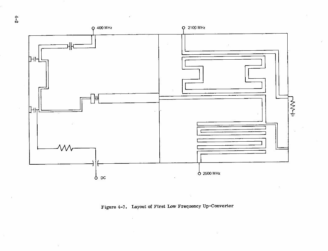
transmission line elements result which increases the sensitivity to normal tolerancevariation. Furthermore, the use of wide transmission lines is limited to lines whosewidths are less than one-quarter wavelength; otherwise the behaviour of the transmissionline elements becomes unpredictable.
Various circuit configurations using both series and shunt mounted diodes wereanalyzed on computer. The best arrangement found is shown in Figure 4-6. The pumpand output VSWR are about 1.5:1 while the input mismatch loss is less than 10 dB.
SIGNALINPUT400MHz
OUTPUT15GHz
PUMPINPUT14.6 GHz
Figure 4-6. Layout of Single Stage Ku-Band Modulator
4-12

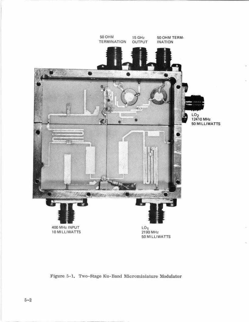
Section 5
MEASURED PERFORMANCE
A photograph of the two stage Ku-band Microminiature Modulator is shown in Figure5-1. The first stage is fabricated on two 1" by 1" alumina substrates, while the secondstage is on two 1" by 5/8" alumina substrates. The circuit frame is made in two sectionswhich can be separated to permit testing of each stage without having to remount thecircuits. Each section provides a continuous and direct ground current path from theSMA connector to the ground metalization of the substrates because it is machined froma single piece of brass. This insures good VSWR's from the connectors and low radiationeven at Ku-band frequencies.
The diode in the second stage is placed above the substrate and the upper end returnedto ground through a metallic strap. At Ku-band frequencies, it is found that the im-pedance of this strap is too high to provide a good ground return. This is provided bya separate metallic stub with one end resting on the top of the diode and the other endon the substrate. The length and position of this stub is varied to tune this diode andprovide maximum output power. This strap is held in position by epoxies. It is foundthat better performance is achieved with this method rather than bringing the diode toground through a hole in the substrate.
Tuning of the circuit is done with strips of indium. The size and location of the stripsare adjusted to give optimum performance and then secured in position with epoxy.The resulting performance of two modulators of this configuration is given in Table5-1. It can be seen that the midband output is about 3.4 dBm, and that the output fallsabout 2 dBm over the 100 MHz band.
The single stage modulator is shown in the photograph in Figure 5-2. It is fabricatedon a 10 mil thick quartz substrate which is 1 in. by 1/2 in. The circuit frame also usesa single piece of brass to provide a continuous direct ground current path from connectorto substrate. The only adjustment needed in this circuit is the length and position ofthe metallic strip attached to the top of the diode. Other tuning is unnecessary becauseof the circuit simplicity, the independence of input and output circuits, and the use ofquartz substrates. The performance of three modulators built in this configuration isalso shown in Table 5-1. It can be seen that the typical midband output is about +8.5 dBmand that the output drops only 1 dB over the 100 MHz band.
5-1
50 OHM 15 GHz TERMINATION OUTPUT
50 OHM TERMINATION
400 MHz INPUT 10 MILLIWATTS
LOT
2190MHz 50 MILLIWATTS
L 0 2
12410 MHz 50 MILLIWATTS
Figure 5-1. Two-Stage Ku-Band Microminiature Modulator
2

Table 5-1. Power Output as a Function of Input Frequencyfor the Five Delivered Modulators
Freq. Unit 1 Unit 2 Unit 3 Unit 5|
275 8.7 7.7 8.5
300 -0.6 9.0 7.9 8.6
325 -1.6 0.9 9.0 8.0 8.7
350 1.5 2.2 8.8 8.0 8.7
375 3.4 3.4 8.7 7.9 8.7
400 3.4 3.3 8.8 8.0 8.7
425 2.4 2.2 8.2 7.7 8.6
450 1.3 0.9 7.8 7.0 8.2
475 -3.0 -0.3 7.6 7.0 8.1
500 -1.9 7.2 6.7 7.8
525 6.2 5.9 7.0
550 5.9 5.3 6.7
575 5.6 4.9 6.0
600 4.6 4.0 5.0
Two-Stage Single Stage
5-3

• •
t *
Figure 5-2. Single Stage Ku-Band Microminiature Modulator
5-4

Section 6
NEW TECHNOLOGY
Ferrite circulators utilizing Microstrip techniques were developed for operation atKu-band frequencies. They were 255 mils in diameter, 25 mils thick, and had a 1 dBinsertion loss, 12 dB isolation band of 10. 5 GHz to 18 GHz.
MIC bandpass filters utilizing hairpin resonators have been developed at 2.1 GHz and at2.5 GHz to achieve maximum utilization of substrate area. These filters have a 1 dBinsertion loss and a 0. 5 dB bandwidth of 100 MHz.
Fused quarty substrates have been utilized at Ku-band frequencies to achieve bettercircuit performance. A wider range of characteristic impedance is available andtransmission line lengths are not as critical.
Computer aided design (CAD) techniques have been modified to improve correlationwith measured performance at Ku-band frequencies. The model for microstrip trans-mission lines now includes a built in correction for dispersion effects.
Circuit frames have been developed to improve the VSWR at the connectors and to re-duce radiation effects at Ku-band. Previously, base blocks and surrounding frameswere separate pieces held together by two screws. In the worst case, ground currentswould be forced through a long path including these screws to get from the connectorto the substrate. Now a single piece of brass is used to form the complete base blockand to minimize the ground current path length.
6-1/6-2

Section 7
CONCLUSIONS AND RECOMMENDATIONS
The output power as a function of frequency for the five modulators is shown in Figure7-1. It can be seen that the single stage units have about 5 dB greater output and muchgreater bandwidth than the double stage modulators. In addition, these units are only20% of the size and weight of the larger units.
As a result of this program, the following recommendations can be made when designingKu-band varactor diode up-converters.
a. The Ku-band circuitry should be on 10 mil thick quartz substrates. This re-sults in reasonable dimensions for transmission line elements and permits awider range of characteristic impedances to be used.
b. The ratio of output frequency to input frequency should be higher than 10 to1. This results in much simpler circuitry. If any tuning is necessary, itcan usually be done without upsetting other frequency components becausesimple capacitors, inductors, or stubs can be used to eliminate interaction.Another advantage is that any multiples of the input frequency that fall withinthe output passband will be low in level because of the high order of multi-plication required.
c. The up-conversion should be done in as few stages as possible. This elimi-nates losses in interstage matching networks and completely avoids theproblem of parametric oscillations frequently encountered when two or morestages are cascaded. The resulting circuits have smaller size and weight.
7-1

co
~og'
.LO
J.0
.-_j-J
_l. J
-J
aa,, a
zC
o 5
1 QN
a0 I N
N)
- D=
N
0
0LJ
oz zi
tt)I--
_ _:
-i -i
oM
o0
0
....J
Wmmm00.
J
_
Z W
W
p-"-
I (D
N
0
LU
_
Iz
I
mc
C,.r
,CT,I j
I .
I00i
/
/
////
C',
(J0p-
ci,-UJ
z-CD
z 1.1.
UI
cnU,
wCD
zp-
0b
0 U
)
uIp
-3M
Od
NdL
NO
WG
P
-H
3M
~d
lfldilo
o
.0
00to C
O
0('3
o 0
InLO
*-4
90)
o 0
o
o 0q
LO
4-4
0
U
0oz_
OW
O
hI-
L.
rn 40
I 0 C4eg
p)
o 0C
1N h
0n A~~~0s-
o~
~
o 0
I)ntNN
If)N
7-2
IL
IL

Appendix
REFERENCES
1. Penfield and Rafuse, Varactor Applications, MIT Press, 1962
2. Grayzel, "A Note on the Abrupt Junction Large Signal Upconverter", Proc. IEEE,Jan. 1966, pp. 78-9.
3. Matthaei, Young, and Jones, Design of Microwave Filters, Impedance-MatchingNetworks, and Coupling Structures, McGraw Hill 1964.
4. Giannini, Angliel, Camisa, "An L-Band MIC Front End for an IFF Receiver",IEEE, Trans MTT, July, 1971, pp. 622-627.
5. Miura and Hashimoto, "A New Concept for Broadbanding the Ferrite SubstrateCirculator Based on Experimental Modal Analysis", 1971 IEEE-GMTT InternationMicrowave Symposium Digest, pp. 80-81.
6. T. S. Osborne, "Design of Efficient Broadband Varactor Upconverters", BSTJ,July - August, 1969, pp. 1623-1649.
A- 1/A-2


![Miniature Ka-band Low Noise Amplifier (Ka-LNA) · PDF fileNTS-PRM-14007Rev.2 Miniature Ka-band Low Noise Amplifier (Ka-LNA) 40 41 42 43 44 45 46 47 48 49 50 26.0 28.5 31.0 Gain [dB]](https://img.pdfslide.us/doc/110x75/5a7873ed7f8b9a87198b7cf8/miniature-ka-band-low-noise-amplifier-ka-lna-a-nts-prm-14007rev2-miniature.jpg)