Embed Size (px)
Citation preview

REV. D
Information furnished by Analog Devices is believed to be accurate andreliable. However, no responsibility is assumed by Analog Devices for itsuse, nor for any infringements of patents or other rights of third parties thatmay result from its use. No license is granted by implication or otherwiseunder any patent or patent rights of Analog Devices.
aAD202/AD204
One Technology Way, P.O. Box 9106, Norwood, MA 02062-9106, U.S.A.
Tel: 781/329-4700 www.analog.com
Fax: 781/326-8703 © Analog Devices, Inc., 2002
Low Cost, MiniatureIsolation Amplifiers
FEATURES
Small Size: 4 Channels/lnch
Low Power: 35 mW (AD204)
High Accuracy: 0.025% Max Nonlinearity (K Grade)
High CMR: 130 dB (Gain = 100 V/V)
Wide Bandwidth: 5 kHz Full-Power (AD204)
High CMV Isolation: 2000 V pk Continuous (K Grade)
(Signal and Power)
Isolated Power Outputs
Uncommitted Input Amplifier
APPLICATIONS
Multichannel Data Acquisition
Current Shunt Measurements
Motor Controls
Process Signal Isolation
High Voltage Instrumentation Amplifier
GENERAL DESCRIPTIONThe AD202 and AD204 are general purpose, two-port, trans-former-coupled isolation amplifiers that may be used in a broadrange of applications where input signals must be measured,processed, and/or transmitted without a galvanic connection.These industry standard isolation amplifiers offer a completeisolation function, with both signal and power isolation providedfor in a single compact plastic SIP or DIP style package. Theprimary distinction between the AD202 and the AD204 is thatthe AD202 is powered directly from a 15 V dc supply while theAD204 is powered by an externally supplied clock, such as therecommended AD246 Clock Driver.
The AD202 and AD204 provide total galvanic isolation betweenthe input and output stages of the isolation amplifier throughthe use of internal transformer-coupling. The functionally com-plete AD202 and AD204 eliminate the need for an external,user-supplied dc-to-dc converter. This permits the designerto minimize the necessary circuit overhead and consequentlyreduce the overall design and component costs.
The design of the AD202 and AD204 emphasizes maximumflexibility and ease of use, including the availability of anuncommitted op amp on the input stage. They feature a bipolar± 5 V output range, an adjustable gain range of from 1V/V to100 V/V, ± 0.025% max nonlinearity (K grade), 130 dB ofCMR, and the AD204 consumes a low 35 mW of power.
The functional block diagrams can be seen in Figures 1a and 1b.
PRODUCT HIGHLIGHTSThe AD202 and AD204 are full-featured isolators offeringnumerous benefits to the user:
Small Size: The AD202 and AD204 are available in SIP andDIP form packages. The SIP package is just 0.25" wide, givingthe user a channel density of four channels per inch. The isolationbarrier is positioned to maximize input to output spacing. Forapplications requiring a low profile, the DIP package provides aheight of just 0.350".
High Accuracy: With a maximum nonlinearity of ± 0.025%for the AD202K/AD204K (± 0.05% for the AD202J/AD204J)and low drift over temperature, the AD202 and AD204 providehigh isolation without loss of signal integrity.
Low Power: Power consumption of 35 mW (AD204) and75 mW (AD202) over the full signal range makes these isolatorsideal for use in applications with large channel counts or tightpower budgets.
Wide Bandwidth: The AD204’s full-power bandwidth of 5 kHzmakes it useful for wideband signals. It is also effective in appli-cations like control loops, where limited bandwidth could resultin instability.
Excellent Common-Mode Performance: The AD202K/AD204K provide ± 2000 V pk continuous common-mode isola-tion, while the AD202J/AD204J provide ± 1000 V pk continuouscommon-mode isolation. All models have a total common-modeinput capacitance of less than 5 pF inclusive of power isolation.This results in CMR ranging from 130 dB at a gain of 100 dB to104 dB (minimum at unity gain) and very low leakage current(2 mA maximum).
Flexible Input: An uncommitted op amp is provided at theinput of all models. This provides buffering and gain as required,and facilitates many alternative input functions including filtering,summing, high voltage ranges, and current (transimpedance) input.
Isolated Power: The AD204 can supply isolated power of± 7.5 V at 2 mA. This is sufficient to operate a low-drift inputpreamp, provide excitation to a semiconductor strain gage, orpower any of a wide range of user-supplied ancillary circuits.The AD202 can supply ± 7.5 V at 0.4 mA, which is sufficient tooperate adjustment networks or low power references and opamps, or to provide an open-input alarm.

REV. D–2–
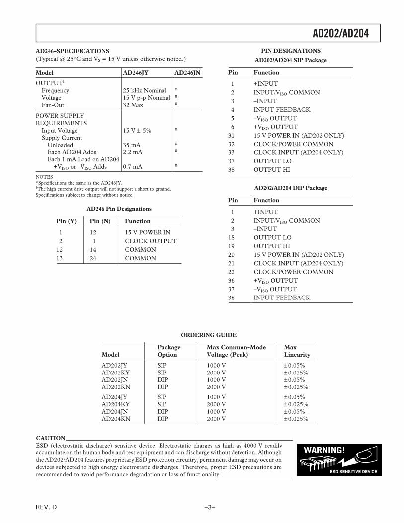
AD202/AD204–SPECIFICATIONSModel AD204J AD204K AD202J AD202K
GAINRange 1 V/V–100 V/V * * *Error ± 0.5% typ (± 4% max) * * *vs. Temperature ± 20 ppm/∞C typ (± 45 ppm/∞C max) * * *vs. Time ± 50 ppm/1000 Hours * * *vs. Supply Voltage ± 0.01%/V ± 0.01%/V ± 0.01%/V ± 0.01%/VNonlinearity (G = 1 V/V)1 ± 0.05% max ± 0.025% max ± 0.05% max ± 0.025% maxNonlinearity vs. Isolated Supply Load ± 0.0015%/mA * * *
INPUT VOLTAGE RATINGSInput Voltage Range ± 5 V * * *Max lsolation Voltage (Input to Output)
AC, 60 Hz, Continuous 750 V rms 1500 V rms 750 V rms 1500 V rmsContinuous (AC and DC) ± 1000 V Peak ± 2000 V Peak ± 1000 V Peak ± 2000 V Peak
Isolation-Mode Rejection Ratio (IMRR) @ 60 HzRS £ 100 W (HI and LO Inputs) G = 1 V/V 110 dB 110 dB 105 dB 105 dB
G = 100 V/V 130 dB * * *RS £ l kW (Input HI, LO, or Both) G = 1 V/V 104 dB min 104 dB min 100 dB min 100 dB min G = 100 V/V 110 dB min * * *
Leakage Current Input to Output @ 240 V rms, 60 Hz 2 mA rms max * * *
INPUT IMPEDANCEDifferential (G = 1 V/V) 1012 W * * *Common-Mode 2 GW4.5 pF * * *
INPUT BIAS CURRENTInitial, @ 25∞C ± 30 pA * * *vs. Temperature (0∞C to 70∞C) ± 10 nA * * *
INPUT DIFFERENCE CURRENTInitial, @ 25∞C ± 5 pA * * *vs. Temperature (0∞C to 70∞C) ± 2 nA * * *
INPUT NOISEVoltage, 0.1 Hz to 100 Hz 4 mV p-p * * *
f > 200 Hz 50 nV/÷Hz * * *
FREQUENCY RESPONSEBandwidth (VO £ 10 V p-p, G = 1 V–50 V/V) 5 kHz 5 kHz 2 kHz 2 kHzSettling Time, to ± 10 mV (10 V Step) 1 ms * * *
OFFSET VOLTAGE (RTI)Initial, @ 25∞C Adjustable to Zero (± 15 ± 15/G)mV max (± 5 ± 5/G) mV max (± 15 ± 15/G) mV max (± 5 ± 5/G) mV max
vs. Temperature (0∞C to 70∞C)
± ± ∞ÊËÁ
ˆ¯
1010G
V Cm * * *
RATED OUTPUTVoltage (Out HI to Out LO) ± 5 V * * *Voltage at Out HI or Out LO (Ref. Pin 32) ± 6.5 V * * *Output Resistance 3 kW 3 kW 7 kW 7 kWOutput Ripple, 100 kHz Bandwidth 10 mV p-p * * *
5 kHz Bandwidth 0.5 mV rms * * *
ISOLATED POWER OUTPUT2
Voltage, No Load ± 7.5 V * * *Accuracy ± 10% * * *Current 2 mA (Either Output)3 2 mA (Either Output)3 400 mA Total 400 mA TotalRegulation, No Load to Full Load 5% * * *Ripple 100 mV p-p * * *
OSCILLATOR DRIVE INPUTInput Voltage 15 V p-p Nominal 15 V p-p Nominal N/A N/AInput Frequency 25 kHz Nominal 25 kHz Nominal N/A N/A
POWER SUPPLY (AD202 Only)Voltage, Rated Performance N/A N/A 15 V ± 5% 15 V ± 5%Voltage, Operating N/A N/A 15 V ± 10% 15 V ± 10%Current, No Load (VS = 15 V) N/A N/A 5 mA 5 mA
TEMPERATURE RANGERated Performance 0∞C to 70∞C * * *Operating –40∞C to +85∞C * * *Storage –40∞C to +85∞C * * *
PACKAGE DIMENSIONS4
SIP Package (Y) 2.08" ¥ 0.250" ¥ 0.625" * * *DlP Package (N) 2.10" ¥ 0.700" ¥ 0.350" * * *
(Typical @ 25C and VS = 15 V unless otherwise noted.)
NOTES*Specifications same as AD204J.1Nonlinearity is specified as a % deviation from a best straight line.21.0 mF min decoupling required (see text).
33 mA with one supply loaded.4Width is 0.25" typ, 0.26" max.Specifications subject to change without notice.
REV. D
AD202/AD204
–3–
AD246–SPECIFICATIONS(Typical @ 25∞C and VS = 15 V unless otherwise noted.)
Model AD246JY AD246JN
OUTPUTl
Frequency 25 kHz Nominal *Voltage 15 V p-p Nominal *Fan-Out 32 Max *
POWER SUPPLYREQUIREMENTS
Input Voltage 15 V ± 5% *Supply Current
Unloaded 35 mA *Each AD204 Adds 2.2 mA *Each 1 mA Load on AD204
+VISO or –VISO Adds 0.7 mA *
NOTES*Specifications the same as the AD246JY.1The high current drive output will not support a short to ground.Specifications subject to change without notice.
AD246 Pin Designations
Pin (Y) Pin (N) Function
1 12 15 V POWER IN2 1 CLOCK OUTPUT
12 14 COMMON13 24 COMMON
ORDERING GUIDE
Package Max Common-Mode MaxModel Option Voltage (Peak) Linearity
AD202JY SIP 1000 V ± 0.05%AD202KY SIP 2000 V ± 0.025%AD202JN DIP 1000 V ± 0.05%AD202KN DIP 2000 V ± 0.025%
AD204JY SIP 1000 V ± 0.05%AD204KY SIP 2000 V ± 0.025%AD204JN DIP 1000 V ± 0.05%AD204KN DIP 2000 V ± 0.025%
CAUTIONESD (electrostatic discharge) sensitive device. Electrostatic charges as high as 4000 V readilyaccumulate on the human body and test equipment and can discharge without detection. Althoughthe AD202/AD204 features proprietary ESD protection circuitry, permanent damage may occur ondevices subjected to high energy electrostatic discharges. Therefore, proper ESD precautions arerecommended to avoid performance degradation or loss of functionality.
WARNING!
ESD SENSITIVE DEVICE
PIN DESIGNATIONS
AD202/AD204 SIP Package
Pin Function
1 +INPUT2 INPUT/VISO COMMON3 –INPUT4 INPUT FEEDBACK5 –VISO OUTPUT6 +VISO OUTPUT
31 15 V POWER IN (AD202 ONLY)32 CLOCK/POWER COMMON33 CLOCK INPUT (AD204 ONLY)37 OUTPUT LO38 OUTPUT HI
AD202/AD204 DIP Package
Pin Function
1 +INPUT2 INPUT/VISO COMMON3 –INPUT
18 OUTPUT LO19 OUTPUT HI20 15 V POWER IN (AD202 ONLY)21 CLOCK INPUT (AD204 ONLY)22 CLOCK/POWER COMMON36 +VISO OUTPUT37 –VISO OUTPUT38 INPUT FEEDBACK

REV. D
AD202/AD204
–4–
DIFFERENCES BETWEEN THE AD202 AND AD204The primary distinction between the AD202 and AD204 is inthe method by which they are powered: the AD202 operatesdirectly from 15 V dc while the AD204 is powered by a non-isolated externally-supplied clock (AD246) that can drive up to32 AD204s. The main advantages of using the externally-clocked AD204 over the AD202 are reduced cost in multichannelapplications, lower power consumption, and higher bandwidth.In addition, the AD204 can supply substantially more isolatedpower than the AD202.
Of course, in a great many situations, especially where only oneor a few isolators are used, the convenience of standalone opera-tion provided by the AD202 will be more significant than anyof the AD204’s advantages. There may also be cases where it isdesirable to accommodate either device interchangeably, so thepinouts of the two products have been designed to make thateasy to do.
RECTAND
FILTEROSCILLATOR
DEMODMOD
SIGNAL
POWER
5VFS
+7.5V
–7.5V25kHz 25kHz
AD202FB
IN–
IN+
IN COM
VSIG
+VISO OUT
–VISO OUT
5VFS
HI
LO
15V DC
POWERRETURN
VOUT
Figure 1a. AD202 Functional Block Diagram
RECTAND
FILTER
POWERCONV.
DEMODMOD
SIGNAL
POWER
5VFS
+7.5V
–7.5V25kHz 25kHz
AD204FB
IN–
IN+
IN COM
VSIG
+VISO OUT
–VISO OUT
5VFS
HI
LO
CLOCK15V p-p25kHz
POWERRETURN
VOUT
Figure 1b. AD204 Functional Block Diagram (Pin Designations Apply to the DIP-Style Package)
INSIDE THE AD202 AND AD204The AD202 and AD204 use an amplitude modulation techniqueto permit transformer coupling of signals down to dc (Figure 1aand 1b). Both models also contain an uncommitted input opamp and a power transformer that provides isolated power tothe op amp, the modulator, and any external load. The powertransformer primary is driven by a 25 kHz, 15 V p-p squarewave generated internally in the case of the AD202, or suppliedexternally for the AD204.
Within the signal swing limits of approximately ±5 V, the out-put voltage of the isolator is equal to the output voltage of theop amp; that is, the isolation barrier has unity gain. The outputsignal is not internally buffered, so the user is free to interchange
the output leads to get signal inversion. Additionally, in multi-channel applications, the unbuffered outputs can be multiplexedwith one buffer following the mux. This technique minimizesoffset errors while reducing power consumption and cost. Theoutput resistance of the isolator is typically 3 kΩ for the AD204(7 kΩ for AD202) and varies with signal level and temperature,so it should not be loaded (see Figure 2 for the effects of loadupon nonlinearity and gain drift). In many cases, a high imped-ance load will be present or a following circuit such as an outputfilter can serve as a buffer so that a separate buffer function willnot often be needed.
OUTPUT LOAD – M
0.25
0.20
00 1.00.1 0.2 0.3 0.4 0.5 0.6 0.7 0.8 0.9
0.15
0.10
0.05
–10
–8
–6
–4
–2
0
–500
–400
–300
–200
–100
0
GAINCHANGE
(%)
GAIN TCCHANGE(ppm/C)
NON-LINEARITY
(%)
AD202 GAIN AND GAIN TC
AD202 NONLINEARITY
AD204 NONLINEARITY
AD204 GAIN AND GAIN TC
Figure 2. Effects of Output Loading
USING THE AD202 AND AD204Powering the AD202. The AD202 requires only a single 15 Vpower supply connected as shown in Figure 3a. A bypass capaci-tor is provided in the module.
15V 5%
15V RETURN
AD202
Figure 3a.
Powering the AD204. The AD204 gets its power from anexternally supplied clock signal (a 15 V p-p square wave with anominal frequency of 25 kHz) as shown in Figure 3b.
15V
15V RETURN
AD204 AD204 AD204
AD246
+
Figure 3b.
(NOTE: Circuit figures shown on this page are for SIP-style packages. Refer toPage 3 for proper DIP package pinout.)

REV. D
AD202/AD204
–5–
AD246 Clock Driver. The AD246 is a compact, inexpensiveclock driver that can be used to obtain the required clock from asingle 15 V supply. Alternatively, the circuit shown in Figure 4(essentially an AD246) can be used. In either case, one clockcircuit can operate at least 32 AD204s at the rated minimumsupply voltage of 14.25 V and one additional isolator can beoperated for each 40 mV increase in supply voltage up to 15 V.
A supply bypass capacitor is included in the AD246, but if manyAD204s are operated from a single AD246, an external bypasscapacitor should be used with a value of at least 1 mF for everyfive isolators used. Place the capacitor as close as possible to theclock driver.
180pF
49.9k
C
RC
R2
3
1
QCD4047B
14 6 5
12 9 8 7 4
10 2
4
TELEDYNETSC426
3
1N914
1N914
6
7
5 +1F35V
15V
CLKOUT
CLK ANDPWR COM
Figure 4. Clock Driver
Input Configurations. The AD202 and AD204 have beendesigned to be very easy to use in a wide range of applications.The basic connection for standard unity gain applications, usefulfor signals up to ± 5 V, is shown in Figure 5; some of the possiblevariations are described below. When smaller signals must behandled, Figure 6 shows how to achieve gain while preserving avery high input resistance. The value of feedback resistor RF
should be kept above 20 kW for best results. Whenever a gain ofmore than five is taken, a 100 pF capacitor from FB to IN COMis required. At lower gains this capacitor is unnecessary, but itwill not adversely affect performance if used.
OUTHI
OUTLO
IN–
IN+
IN COM
15V ORCLOCKAD202
ORAD204
VOUT5V
2k(SEE TEXT)
VSIG(5V)
FB
Figure 5. Basic Unity-Gain Application
AD202OR
AD204
2k
VSIG
VO
VO = VSIG 1 + –––
RF 20k
RFRG
RF
RG
100pF
( )
Figure 6. Input Connections for Gain > 1
The noninverting circuit of Figures 5 and 6 can also be used toyour advantage when a signal inversion is needed: just interchangeeither the input leads or the output leads to get inversion. Thisapproach retains the high input resistance of the noninvertingcircuit, and at unity gain no gain-setting resistors are needed.
When the isolator is not powered, a negative input voltage ofmore than about 2 V will cause an input current to flow. If thesignal source can supply more than a few mA under such con-ditions, the 2 kW resistor shown in series with IN+ should beused to limit current to a safe value. This is particularly impor-tant with the AD202, which may not start if a large input currentis present.
Figure 7 shows how to accommodate current inputs or sumcurrents or voltages. This circuit can also be used when theinput signal is larger than the ± 5 V input range of the isolator;for example, a ± 50 V input span can be accommodated withRF = 20 kW and RS = 200 kW. Once again, a capacitor from FBto IN COM is required for gains above five.
AD202OR
AD204RS2
V
V = – (VS1 ––– + VS2 ––– + IS RF + ...)RF 20k
RFRS1
RFRS2
RF
RS1
IS
VS1
VS2
Figure 7. Connections for Summing or Current Inputs
(NOTE: Circuit figures shown on this page are for SIP-style packages. Refer toPage 3 for proper DIP package pinout.)
REV. D
AD202/AD204
–6–
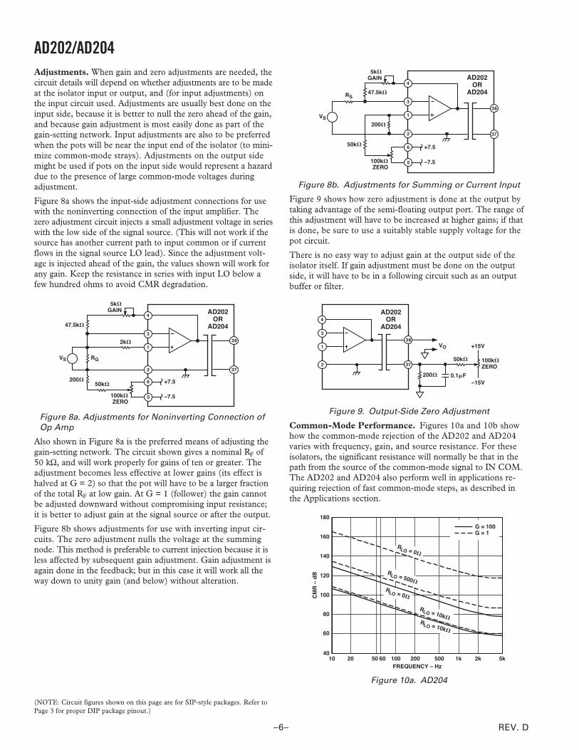
Adjustments. When gain and zero adjustments are needed, thecircuit details will depend on whether adjustments are to be madeat the isolator input or output, and (for input adjustments) onthe input circuit used. Adjustments are usually best done on theinput side, because it is better to null the zero ahead of the gain,and because gain adjustment is most easily done as part of thegain-setting network. Input adjustments are also to be preferredwhen the pots will be near the input end of the isolator (to mini-mize common-mode strays). Adjustments on the output sidemight be used if pots on the input side would represent a hazarddue to the presence of large common-mode voltages duringadjustment.
Figure 8a shows the input-side adjustment connections for usewith the noninverting connection of the input amplifier. Thezero adjustment circuit injects a small adjustment voltage in serieswith the low side of the signal source. (This will not work if thesource has another current path to input common or if currentflows in the signal source LO lead). Since the adjustment volt-age is injected ahead of the gain, the values shown will work forany gain. Keep the resistance in series with input LO below afew hundred ohms to avoid CMR degradation.
AD202OR
AD20447.5k
VS
5kGAIN
RG
200 +7.5
–7.5100kZERO
2k
50k
Figure 8a. Adjustments for Noninverting Connection ofOp Amp
Also shown in Figure 8a is the preferred means of adjusting thegain-setting network. The circuit shown gives a nominal RF of50 kW, and will work properly for gains of ten or greater. Theadjustment becomes less effective at lower gains (its effect ishalved at G = 2) so that the pot will have to be a larger fractionof the total RF at low gain. At G = 1 (follower) the gain cannotbe adjusted downward without compromising input resistance;it is better to adjust gain at the signal source or after the output.
Figure 8b shows adjustments for use with inverting input cir-cuits. The zero adjustment nulls the voltage at the summingnode. This method is preferable to current injection because it isless affected by subsequent gain adjustment. Gain adjustment isagain done in the feedback; but in this case it will work all theway down to unity gain (and below) without alteration.
AD202OR
AD204RS47.5k
VS
5kGAIN
200
50k +7.5
–7.5100kZERO
Figure 8b. Adjustments for Summing or Current Input
Figure 9 shows how zero adjustment is done at the output bytaking advantage of the semi-floating output port. The range ofthis adjustment will have to be increased at higher gains; if thatis done, be sure to use a suitably stable supply voltage for thepot circuit.
There is no easy way to adjust gain at the output side of theisolator itself. If gain adjustment must be done on the outputside, it will have to be in a following circuit such as an outputbuffer or filter.
AD202OR
AD204
200
50k 100kZERO
0.1F
+15V
–15V
VO
Figure 9. Output-Side Zero Adjustment
Common-Mode Performance. Figures 10a and 10b showhow the common-mode rejection of the AD202 and AD204varies with frequency, gain, and source resistance. For theseisolators, the significant resistance will normally be that in thepath from the source of the common-mode signal to IN COM.The AD202 and AD204 also perform well in applications re-quiring rejection of fast common-mode steps, as described inthe Applications section.
FREQUENCY – Hz
180
10
CM
R –
dB
160
140
120
100
80
60
4020 50 60 100 200 500 1k 2k 5k
G = 100G = 1
RLO = 10k
RLO = 500
RLO = 0
RLO = 0
RLO = 10k
Figure 10a. AD204
(NOTE: Circuit figures shown on this page are for SIP-style packages. Refer toPage 3 for proper DIP package pinout.)

REV. D
AD202/AD204
–7–
FREQUENCY – Hz
180
10
CM
R –
dB
160
140
120
100
80
60
4020 50 60 100 200 500 1k 2k 5k
G = 100G = 1
RLO = 10k
RLO = 500
RLO = 0
RLO = 0
RLO = 10k
Figure 10b. AD202
Dynamics and Noise. Frequency response plots for the AD202and AD204 are given in Figure 11. Since neither isolator is slew-rate limited, the plots apply for both large and small signals.Capacitive loads of up to 470 pF will not materially affect fre-quency response. When large signals beyond a few hundred Hzwill be present, it is advisable to bypass –VISO and +VISO to INCOM with 1 mF tantalum capacitors even if the isolated suppliesare not loaded.
At 50 Hz/60 Hz, phase shift through the AD202/AD204 is typically0.8∞ (lagging). Typical unit to unit variation is ± 0.2∞ (lagging).
FREQUENCY – Hz10
VO
/VI –
dB
60
–4020 50 100 200 500 1k 2k 5k
40
20
0
–20
10k 20k
AD204AD202
AMPLITUDERESPONSE
PHASERESPONSE
(G = 1)
0
–50
–100
PH
AS
E D
EG
RE
ES
Figure 11. Frequency Response at Several Gains
The step response of the AD204 for very fast input signals canbe improved by the use of an input filter, as shown in Figure 12.The filter limits the bandwidth of the input (to about 5.3 kHz)so that the isolator does not see fast, out-of-band input termsthat can cause small amounts (± 0.3%) of internal ringing. TheAD204 will then settle to ± 0.1% in about 300 ms for a 10 Vstep.
AD204
3.3k
0.01FVS
Figure 12. Input Filter for Improved Step Response
Except at the highest useful gains, the noise seen at the outputof the AD202 and AD204 will be almost entirely comprised ofcarrier ripple at multiples of 25 kHz. The ripple is typically2 mV p-p near zero output and increases to about 7 mV p-p foroutputs of ± 5 V (1 MHz measurement bandwidth). Adding acapacitor across the output will reduce ripple at the expense ofbandwidth: for example, 0.05 mF at the output of the AD204will result in 1.5 mV ripple at ± 5 V, but signal bandwidth willbe down to 1 kHz.
When the full isolator bandwidth is needed, the simple two-poleactive filter shown in Figure 13 can be used. It will reduce rippleto 0.1 mV p-p with no loss of signal bandwidth, and also servesas an output buffer.
An output buffer or filter may sometimes show output spikesthat do not appear at its input. This is usually due to clock noiseappearing at the op amp’s supply pins (since most op amps havelittle or no supply rejection at high frequencies). Another com-mon source of carrier-related noise is the sharing of a groundtrack by both the output circuit and the power input. Figure 13shows how to avoid these problems: the clock/supply port of theisolator does not share ground or 15 V tracks with any signalcircuits, and the op amp’s supply pins are bypassed to signalcommon (note that the grounded filter capacitor goes here aswell). Ideally, the output signal LO lead and the supply com-mon meet where the isolator output is actually measured, e.g.,at an A/D converter input. If that point is more than a few feetfrom the isolator, it may be useful to bypass output LO to sup-ply common at the isolator with a 0.1 mF capacitor.
In applications where more than a few AD204s are driven by asingle clock driver, substantial current spikes will flow in thepower return line and in whichever signal out lead returns to alow impedance point (usually output LO). Both of these tracksshould be made large to minimize inductance and resistance;ideally, output LO should be directly connected to a groundplane which serves as measurement common.
Current spikes can be greatly reduced by connecting a smallinductance (68 mH–100 mH) in series with the clock pin of eachAD204. Molded chokes such as the Dale IM-2 series, with dcresistance of about 5 W, are suitable.
AD202OR
AD204
10k
2200pF
10k
1000pF
AD711
1.0F 1.0F
POINT OFMEASUREMENT
AD246(IF USED)
POWERSUPPLY
–15V C +15V
+ +
Figure 13. Output Filter Circuit Showing Proper Grounding
(NOTE: Circuit figures shown on this page are for SIP-style packages. Refer toPage 3 for proper DIP package pinout.)
REV. D
AD202/AD204
–8–
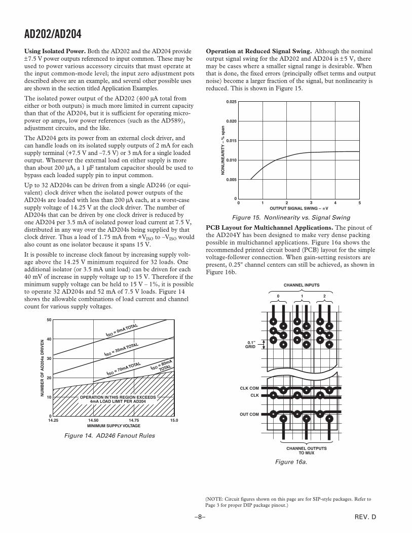
Using Isolated Power. Both the AD202 and the AD204 provide± 7.5 V power outputs referenced to input common. These may beused to power various accessory circuits that must operate atthe input common-mode level; the input zero adjustment potsdescribed above are an example, and several other possible usesare shown in the section titled Application Examples.
The isolated power output of the AD202 (400 mA total fromeither or both outputs) is much more limited in current capacitythan that of the AD204, but it is sufficient for operating micro-power op amps, low power references (such as the AD589),adjustment circuits, and the like.
The AD204 gets its power from an external clock driver, andcan handle loads on its isolated supply outputs of 2 mA for eachsupply terminal (+7.5 V and –7.5 V) or 3 mA for a single loadedoutput. Whenever the external load on either supply is morethan about 200 mA, a 1 mF tantalum capacitor should be used tobypass each loaded supply pin to input common.
Up to 32 AD204s can be driven from a single AD246 (or equi-valent) clock driver when the isolated power outputs of theAD204s are loaded with less than 200 mA each, at a worst-casesupply voltage of 14.25 V at the clock driver. The number ofAD204s that can be driven by one clock driver is reduced byone AD204 per 3.5 mA of isolated power load current at 7.5 V,distributed in any way over the AD204s being supplied by thatclock driver. Thus a load of 1.75 mA from +VISO to –VISO wouldalso count as one isolator because it spans 15 V.
It is possible to increase clock fanout by increasing supply volt-age above the 14.25 V minimum required for 32 loads. Oneadditional isolator (or 3.5 mA unit load) can be driven for each40 mV of increase in supply voltage up to 15 V. Therefore if theminimum supply voltage can be held to 15 V – 1%, it is possibleto operate 32 AD204s and 52 mA of 7.5 V loads. Figure 14shows the allowable combinations of load current and channelcount for various supply voltages.
MINIMUM SUPPLY VOLTAGE14.25
NU
MB
ER
OF
AD
204s
DR
IVE
N
50
014.50 14.75
40
30
20
10
15.0
IISO = 0mA TOTAL
IISO = 35mA TOTAL
IISO = 70mA TOTALIISO = 80mA
OPERATION IN THIS REGION EXCEEDS4mA LOAD LIMIT PER AD204
TOTAL
Figure 14. AD246 Fanout Rules
Operation at Reduced Signal Swing. Although the nominaloutput signal swing for the AD202 and AD204 is ± 5 V, theremay be cases where a smaller signal range is desirable. Whenthat is done, the fixed errors (principally offset terms and outputnoise) become a larger fraction of the signal, but nonlinearity isreduced. This is shown in Figure 15.
OUTPUT SIGNAL SWING – V0
NO
NL
INE
AR
ITY
– %
sp
an
0.025
02 3
0.020
0.015
0.010
0.005
51 4
Figure 15. Nonlinearity vs. Signal Swing
PCB Layout for Multichannel Applications. The pinout ofthe AD204Y has been designed to make very dense packingpossible in multichannel applications. Figure 16a shows therecommended printed circuit board (PCB) layout for the simplevoltage-follower connection. When gain-setting resistors arepresent, 0.25" channel centers can still be achieved, as shown inFigure 16b.
CHANNEL INPUTS
0 1 2
0.1”GRID
CLK COM
CLK
OUT COM
CHANNEL OUTPUTSTO MUX
Figure 16a.
(NOTE: Circuit figures shown on this page are for SIP-style packages. Refer toPage 3 for proper DIP package pinout.)

REV. D
AD202/AD204
–9–
CHANNEL 0 CHANNEL 1
HI LO HI LO
RF RG RF RG
100pF 100pF
0.1”GRID
1
3
5
2
4
6
1
3
5
2
4
6
Figure 16b.
Synchronization. Since AD204s operate from a commonclock, synchronization is inherent. AD202s will normally notinteract to produce beat frequencies even when mounted on0.25-inch centers. Interaction may occur in rare situations wherea large number of long, unshielded input cables are bundledtogether and channel gains are high. In such cases, shieldedcable may be required or AD204s can be used.
APPLICATIONS EXAMPLESLow Level Sensor Inputs. In applications where the output oflow level sensors such as thermocouples must be isolated, a lowdrift input amplifier can be used with an AD204, as shown in
Figure 17. A three-pole active filter is included in the design toget normal-mode rejection of frequencies above a few Hz and toprovide enhanced common-mode rejection at 60 Hz. If offsetadjustment is needed, it is best done at the trim pins of the OP07itself; gain adjustment can be done at the feedback resistor.
Note that the isolated supply current is large enough to mandatethe use of 1 mF supply bypass capacitors. This circuit can beused with an AD202 if a low power op amp is used instead ofthe OP07.
Process Current Input with Offset. Figure 18 shows anisolator receiver that translates a 4-20 mA process currentsignal into a 0 V to 10 V output. A 1 V to 5 V signal appears atthe isolator’s output, and a –1 V reference applied to output LOprovides the necessary level shift (in multichannel applications,the reference can be shared by all channels). This technique isoften useful for getting offset with a follower-type output buffer.
AD202OR
AD204
+
+15V
–15V
2504–20mA
1VTO5V
– 15k
+
0VTO10V
10k
–237
1k
AD589
6.8k
–15V
–1V TOADDITIONAL
CHANNELS
Figure 18. Process Current Input Isolator with Offset
The circuit as shown requires a source compliance of at least5 V, but if necessary that can be reduced by using a lower valueof current-sampling resistor and configuring the input amplifierfor a small gain.
(NOTE: Circuit figures shown on this page are for SIP-style packages. Refer toPage 3 for proper DIP package pinout.)
AD204
+7.5V
–7.5V CLK RET
CLK
–
+
VO = VI 1 + 50kRG
0.15F
470k470k
0.038F49.9k
RG
AD OP-07
1F+
1F+
1F+
39k
220M
HI
LO
OPTIONALOPEN INPUTDETECTION
( )
Figure 17. Input Amplifier and Filter for Sensor Signals

REV. D
AD202/AD204
–10–
High Compliance Current Source. In Figure 19, an isolatoris used to sense the voltage across current-sensing resistor RS toallow direct feedback control of a high voltage transistor or FETused as a high compliance current source. Since the isolator hasvirtually no response to dc common-mode voltage, the closed-loop current source has a static output resistance greater than1014 W even for output currents of several mA. The outputcurrent capability of the circuit is limited only by power dissipa-tion in the source transistor.
AD202OR
AD204
100k
+15V
–15V
470pF
10k+5V REF
+
–VC
20k
LOADIL = VCRS
–10V TO +250V
RS1k
MPSU10
1k
Figure 19. High Compliance Current Source
Motor Control Isolator. The AD202 and AD204 performvery well in applications where rejection of fast common-modesteps is important but bandwidth must not be compromised.Current sensing in a fill-wave bridge motor driver (Figure 20) isone example of this class of application. For 200 V common-modesteps (1 ms rise time) and a gain of 50 as shown, the typicalresponse at the isolator output will be spikes of ± 5 mV ampli-tude, decaying to zero in less than 100 ms. Spike height can bereduced by a factor of four with output filtering just beyond theisolator’s bandwidth.
AD204
+
–
5V
M5m
20A
+200V dc
–
100mV
Figure 20. Motor Control Current Sensing
Floating Current Source/Ohmmeter. When a small floatingcurrent is needed with a compliance range of up to ± 1000 V dc,the AD204 can be used to both create and regulate the current.This can save considerable power, since the controlled currentdoes not have to return to ground. In Figure 21, an AD589reference is used to force a small fixed voltage across R. Thatsets the current that the input op amp will have to returnthrough the load to zero its input. Note that the isolator’s out-put isn’t needed at all in this application; the whole job is doneby the input section. However, the signal at the output could beuseful as it’s the voltage across the load, referenced to ground.Since the load current is known, the output voltage is propor-tional to load resistance.
AD204
LOAD
R
7.5V
1F+
30k
AD589
+
–
VO = RLVRR
ILOAD = (2mA MAX)
VLOAD 4V
1.23VR
Figure 21. Floating Current Source
Photodiode Amplifier. Figure 22 shows a transresistanceconnection used to isolate and amplify the output of a photo-diode. The photodiode operates at zero bias, and its outputcurrent is scaled by RF to give a 5 V full-scale output.
AD202OR
AD204
0V TO 5V
500k
PHOTODIODE
10AFS
Figure 22. Photodiode Amplifier
(NOTE: Circuit figures shown on this page are for SIP-style packages. Refer toPage 3 for proper DIP package pinout.)
REV. D
AD202/AD204
–11–
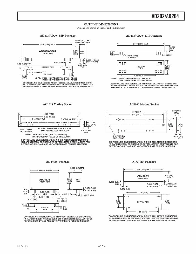
OUTLINE DIMENSIONSDimensions shown in inches and (millimeters)
AD202/AD204 SIP Package
0.625(15.9)MAX
0.15 (3.81) TYP
1 3 5
2 6
31 33 37
38324
0.05 (1.3)TYP1.30 (33.0)
0.010 0.020(0.25 0.51)0.20 (5.1)
0.143(3.63)
0.12(3.05)
0.10 (2.5)TYP
0.250 (6.3) TYP0.260 (6.6) MAX
2.08 (52.8) MAX
FRONT VIEW
BOTTOM VIEWCL
AD202/AD204 SIDEVIEW
NOTE: PIN 31 IS PRESENT ONLY ON AD202 PIN 33 IS PRESENT ONLY ON AD204
CONTROLLING DIMENSIONS ARE IN INCHES; MILLIMETER DIMENSIONS(IN PARENTHESES) ARE ROUNDED-OFF MILLIMETER EQUIVALENTS FORREFERENCE ONLY AND ARE NOT APPROPRIATE FOR USE IN DESIGN
AC1058 Mating Socket
0.30 (7.62) MAX
0.24(6.10)
0.10 (2.5) DIABOTH ENDS
2.65 (7.30)2.50 (63.50)
0.10 (2.50) TYP 0.075 (1.90) TYP
AC1058 CAN BE USED AS A SOCKETFOR AD202,AD204 AND AD246
NOTE: AMP ZP SOCKET (PIN 2 – 382006 – 3) MAY BE USED IN PLACE OF THE AC1058
CONTROLLING DIMENSIONS ARE IN INCHES; MILLIMETER DIMENSIONS(IN PARENTHESES) ARE ROUNDED-OFF MILLIMETER EQUIVALENTS FORREFERENCE ONLY AND ARE NOT APPROPRIATE FOR USE IN DESIGN
AD246JY Package
0.330 (8.4) MAX
0.10 (2.5) NOM
0.625(15.9)MAX
0.115 (2.9)
SIDEVIEW
0.015 (0.38)0.010 (0.25)
1
2
13
12
0.10(2.5)
0.115(2.9)
CLBOTTOM
VIEW
0.05 (1.30)NOM
0.10(2.5)MIN
0.995 (25.3) MAX
AD246JYFRONT VIEW
0.55 (14.0)0.197 (5.0) 0.015 (0.38)
0.010 (0.25)
CONTROLLING DIMENSIONS ARE IN INCHES; MILLIMETER DIMENSIONS(IN PARENTHESES) ARE ROUNDED-OFF MILLIMETER EQUIVALENTS FORREFERENCE ONLY AND ARE NOT APPROPRIATE FOR USE IN DESIGN
AD202/AD204 DIP Package
1.60 (40.6)
BOTTOMVIEW
38 37 36
1 2 3
22 21 20
18 190.700(17.8)MAX
0.015 (0.38)
0.350(8.9)MAX
0.018 (0.46)SQUARE
0.10(2.5)MIN
2.100 (53.3) MAX
NOTE: PIN 20 IS PRESENT ONLY ON AD202 PIN 21 IS PRESENT ONLY ON AD204
CONTROLLING DIMENSIONS ARE IN INCHES; MILLIMETER DIMENSIONS(IN PARENTHESES) ARE ROUNDED-OFF MILLIMETER EQUIVALENTS FORREFERENCE ONLY AND ARE NOT APPROPRIATE FOR USE IN DESIGN
AC1060 Mating Socket
2.35 (59.7)
2.60 (66.0)
0.50(12.7)
0.10 (2.5) DIABOTH ENDS
0.70(17.8)
0.125 (3.1)TYP
0.30 (7.62)MAX
CONTROLLING DIMENSIONS ARE IN INCHES; MILLIMETER DIMENSIONS(IN PARENTHESES) ARE ROUNDED-OFF MILLIMETER EQUIVALENTS FORREFERENCE ONLY AND ARE NOT APPROPRIATE FOR USE IN DESIGN
AD246JN Package
FRONT VIEWAD246JN
1.445 (36.7) MAX
0.100 (2.5)MIN
0.35 (8.9)MAX
0.020 (0.51)0.010 (0.25)
0.145 (3.7)
0.020 (0.51)0.015 (0.38)
1 12
1424
BOTTOM VIEW
1.10 (27.9)
1.00 (25.4)
0. 50(12.7)
0.70(17.8)
CONTROLLING DIMENSIONS ARE IN INCHES; MILLIMETER DIMENSIONS(IN PARENTHESES) ARE ROUNDED-OFF MILLIMETER EQUIVALENTS FORREFERENCE ONLY AND ARE NOT APPROPRIATE FOR USE IN DESIGN

REV. D–12–
C00
483–
0–10
/02(
D)
PR
INT
ED
IN U
.S.A
.
AD202/AD204
Revision HistoryLocation Page
10/02—Data Sheet changed from REV. C to REV. D.
Deleted FUNCTIONAL BLOCK DIAGRAM . . . . . . . . . . . . . . . . . . . . . . . . . . . . . . . . . . . . . . . . . . . . . . . . . . . . . . . . . . . . . . . . . 1
Text added to GENERAL DESCRIPTION . . . . . . . . . . . . . . . . . . . . . . . . . . . . . . . . . . . . . . . . . . . . . . . . . . . . . . . . . . . . . . . . . . . 1
Edits to SPECIFICATIONS TABLE . . . . . . . . . . . . . . . . . . . . . . . . . . . . . . . . . . . . . . . . . . . . . . . . . . . . . . . . . . . . . . . . . . . . . . . . 2
Edits to Figure 4 . . . . . . . . . . . . . . . . . . . . . . . . . . . . . . . . . . . . . . . . . . . . . . . . . . . . . . . . . . . . . . . . . . . . . . . . . . . . . . . . . . . . . . . . 5
Edits to Input Configurations section . . . . . . . . . . . . . . . . . . . . . . . . . . . . . . . . . . . . . . . . . . . . . . . . . . . . . . . . . . . . . . . . . . . . . . . . 5
Edit to High Compliance Current Source section . . . . . . . . . . . . . . . . . . . . . . . . . . . . . . . . . . . . . . . . . . . . . . . . . . . . . . . . . . . . . . 10
Updated OUTLINE DIMENSIONS . . . . . . . . . . . . . . . . . . . . . . . . . . . . . . . . . . . . . . . . . . . . . . . . . . . . . . . . . . . . . . . . . . . . . . . 11
4/01—Data Sheet changed from REV. B to REV. C.
Change to SIP Package . . . . . . . . . . . . . . . . . . . . . . . . . . . . . . . . . . . . . . . . . . . . . . . . . . . . . . . . . . . . . . . . . . . . . . . . . . . . . . . . . . 11