Embed Size (px)
Citation preview

MAX14824
IO-Link Master Transceiver
1
Typical Operating Circuits
19-5788; Rev 3; 5/12
Typical Operating Circuits continued at end of data sheet.
General Description
The MAX14824 is an IO-LinkM master interface that inte-grates an IO-Link physical layer transceiver with an auxiliary digital input and two linear regulators. High port count IO-Link master applications are supported through in-band SPI addressing, and the 12MHz SPI interface minimizes host controller access times. In-band address-ing and selectable SPI addresses enable cascading up to 16 devices.
The device supports all the IO-Link data rates and fea-tures slew-rate-controlled drivers to reduce EMI. The driver is guaranteed to drive up to 300mA (min) load currents. Internal wake-up circuitry automatically deter-mines the correct wake-up polarity, allowing for the use of simple UARTs for wake-up pulse generation.
The MAX14824 is available in a 4mm x 4mm, 24-pin TQFN package with exposed pad, and operates over the extended -40NC to +105NC temperature range.
Applications
IO-Link Master Controllers
PLC Fieldbus Gateways
High Port Count IO-Link Masters
24V Digital Inputs and Outputs
Features
S IO-Link v.1.0 and v.1.1 Physical Layer Compliant
S Supports COM1, COM2, and COM3 Data Rates
S Push-Pull, High-Side, or Low-Side Outputs
S 300mA C/Q Output Drive
S 1µF C/Q Load Drive Capability
S Generates 500mA Wake-Up Pulse
S Automatic Wake-Up Pulse Polarity
S Auxiliary Digital Input
S 5V and 3.3V Linear Regulators
S SPI Interface for Configuration and Monitoring
S SPI-Based Chip Addressing
S EMI Emission Control Through Slew-Controlled Driver
S Reverse-Polarity Protection on DI
S Short-Circuit Protection on C/Q
S High Temperature Warning and Thermal Shutdown
S Extensive Fault Monitoring and Reporting
S -40NC to +105NC Operating Temperature Range
S 4mm x 4mm TQFN Package
IO-Link is a registered trademark of Profibus User Organization (PNO).
Ordering Information appears at end of data sheet.
For related parts and recommended products to use with this part, refer to: www.maxim-ic.com/MAX14824.related
E V A L U A T I O N K I T A V A I L A B L E
MAX14824
1μF1μF 0.1μF
270pF
270pF
LDOIN
C/Q C/Q
SPI
DI
GNDA3A2A1A0GND
24V
V5 VCCVCC LDO33VL TXQ
IO-LINKCONTROLLER
WUENGPO
RXRX
TXCTX
TXENRTS
For pricing, delivery, and ordering information, please contact Maxim Direct at 1-888-629-4642, or visit Maxim’s website at www.maxim-ic.com.

2
MAX14824
IO-Link Master Transceiver
Functional Diagram
MAX14824
UV MONITOR
UV
VCC
V5LDO33 LDOIN
STATUSAND
CONFIGURATION
3.3V LDO
FILTER
DRIVER
WU POLARITYGENERATOR
SHORT-CIRCUITPROTECTION
REVERSEPOLARITY
PROTECTION
5V LDO
VL
SDI
CS
RX
LI
C/Q
DI
GND
C/QLOAD
DILOAD
SDO
SCLK
IRQ
A3:A0
WUEN
TXQ
TXC
TXEN

3
MAX14824
IO-Link Master Transceiver
(All voltages referenced to GND, unless otherwise specified.)VCC ........................................................................-0.3V to +40VLDOIN ....................................................................-0.3V to +40VV5 .......................0.3V to the lesser of (VLDOIN + 0.3V) and +6VLDO33 .................... -0.3V to the lesser of (V5 + 0.3V) and +6VVL .............................................................................-0.3V to +6VDI ............................................................................-40V to +40VC/Q ........................................................... -0.3V to (VCC + 0.3V)Logic Inputs
TXC, TXQ, TXEN, A2, CS, SDI, SCLK, WUEN .. -0.3V to (VL + 0.3V) A3, A1, A0 ...........................................................-0.3V to +6V
Logic Outputs RX, LI, SDO, IRQ ..................................... -0.3V to (VL + 0.3V) UV ........................................................................-0.3V to +6V
Continuous Current Into Any Logic Pin ..........................Q50mAContinuous Power Dissipation
TQFN (derate 27.8mW/NC above +70NC)..................2222mWOperating Temperature Range ........................ -40NC to +105NCMaximum Junction Temperature .....................................+150NCStorage Temperature Range ............................ -65NC to +150NCLead Temperature (soldering, 10s) ................................+300NCSoldering Temperature (reflow) ......................................+260NC
TQFN Junction-to-Ambient Thermal Resistance (BJA) ..........36NC/W Junction-to-Case Thermal Resistance (BJC) .................3NC/W
ABSOLUTE MAXIMUM RATINGS
Note 1: Package thermal resistances were obtained using the method described in JEDEC specification JESD51-7, using a four-layer board. For detailed information on package thermal considerations, refer to www.maxim-ic.com/thermal-tutorial.
Stresses beyond those listed under “Absolute Maximum Ratings” may cause permanent damage to the device. These are stress ratings only, and functional opera-tion of the device at these or any other conditions beyond those indicated in the operational sections of the specifications is not implied. Exposure to absolute maximum rating conditions for extended periods may affect device reliability.
PACKAGE THERMAL CHARACTERISTICS (Note 1)
DC ELECTRICAL CHARACTERISTICS(VCC = 18V to 36V, VL = 2.3V to 5.5V, VGND = 0V; all logic inputs at VL or GND; TA = -40NC to +105NC, unless otherwise noted. Typical values are at VCC = 24V, VL = 3.3V, and TA = +25NC, unless otherwise noted.) (Note 2)
PARAMETER SYMBOL CONDITIONS MIN TYP MAX UNITS
VCC Supply Voltage VCC For driver operation 9 36 V
VCC Supply Current ICC
VCC = 24V, C/Q as input, no load on V5 or LDO33, LDOIN not connected to VCC, VLDOIN = 24V
1.3 2.5 mA
VCC Undervoltage Lockout Threshold
VCCUVLO VCC falling 6 7.5 9 V
VCC Undervoltage Lockout Threshold Hysteresis
VCCUVLO_HYST 200 mV
V5 Supply Current I5_INLDOIN shorted to V5, external 5V applied to V5, no switching, LDO33 disabled
3 mA
V5 Undervoltage Lockout Threshold
V5UVLO V5 falling 2.4 V
VL Logic-Level Supply Voltage VL 2.3 5.5 V
VL Logic-Level Supply Current IL All logic inputs at VL or GND 5 FA
VL Undervoltage Threshold VLUVLO VL falling 0.65 0.95 1.3 V
5V LDO (V5)
LDOIN Input Voltage Range VLDOIN 7 36 V

4
MAX14824
IO-Link Master Transceiver
DC ELECTRICAL CHARACTERISTICS (continued)(VCC = 18V to 36V, VL = 2.3V to 5.5V, VGND = 0V; all logic inputs at VL or GND; TA = -40NC to +105NC, unless otherwise noted. Typical values are at VCC = 24V, VL = 3.3V, and TA = +25NC, unless otherwise noted.) (Note 2)
PARAMETER SYMBOL CONDITIONS MIN TYP MAX UNITS
LDOIN Supply Current ILDOINVLDOIN = 24V, C/Q as input, no load on V5 or LDO33
3.0 5 mA
V5 Output Voltage Range V5 No load on V5, 7V P VLDOIN P 36V 4.75 5.00 5.25 V
V5 Load Regulation1mA < ILOAD < 10mA, VLDOIN = 7V, 0.1FF bypass capacitor on V5
0.08 %
3.3V LDO (LDO33)
LDO33 Output Voltage VLDO33 No load on LDO33 3.1 3.5 V
LDO33 Undervoltage Lockout Threshold
VLDO33UVLO VLDO33 falling 2.4 V
LDO33 Load Regulation 1mA < ILOAD < 10mA, VLDOIN = 7V 0.25 %
24V INTERFACE
C/Q Output Resistance High ROH_C/QC/Q high-side enabled, IC/Q = -200mA, 9V P VCC P 36V (Note 5)
1.8 2.9 I
C/Q Output Resistance Low ROL_C/QC/Q low-side enabled, IC/Q = +200mA, 9V P VCC P 36V (Note 5)
2.0 3.6 I
C/Q Source Current Limit IOH_C/QC/Q high-side enabled, VC/Q < (VCC - 3V), 9V P VCC P 36V
+500 +670 mA
C/Q Sink Current Limit IOL_C/QC/Q low-side enabled, VC/Q > 3V, 9V P VCC P 36V
-660 -500 mA
C/Q Input Threshold High VIH_C/Q C/Q driver disabled 10.5 13.0 V
C/Q Input Threshold Low VIL_C/Q C/Q driver disabled 8.0 11.5 V
C/Q Input Hysteresis VHYS_C/Q C/Q driver disabled 1.0 V
DI Input Threshold High VIH_DI 6.8 8 V
DI Input Threshold Low VIL_DI 5.2 6.4 V
DI Input Hysteresis VHYS_DI 1 V
C/Q Weak Pulldown Current IPDC/Q C/Q driver disabled, VC/Q = VCC 100 400 FA
DI Weak Pulldown Current IPDDI DI load disabled, VDI = VCC 50 300 FA
C/Q Input Capacitance CC/Q C/Q driver disabled 40 pF
DI Input Capacitance CDI 20 pF
C/Q, DI INPUT LOAD
C/Q Load Current ILLM_C/QC/Q load enabled (C/QLoad = 1)
0 P VC/Q P 5V 0 8.1mA
9V P VC/Q 5 6.8 8.1
DI Load Current ILLM_DIDI load enabled (DiLoad = 1)
0 P VDI P 5V 0 4.3mA
9V P VDI 2 3.5 4.3

5
MAX14824
IO-Link Master Transceiver
DC ELECTRICAL CHARACTERISTICS (continued)(VCC = 18V to 36V, VL = 2.3V to 5.5V, VGND = 0V; all logic inputs at VL or GND; TA = -40°C to +105°C, unless otherwise noted. Typical values are at VCC = 24V, VL = 3.3V, and TA = +25NC, unless otherwise noted.) (Note 2)
AC ELECTRICAL CHARACTERISTICS(VCC = 18V to 36V, VL = 2.3V to 5.5V, VGND = 0V; all logic inputs at VL or GND; TA = -40°C to +105°C, unless otherwise noted. Typical values are at VCC = 24V, VL = 3.3V, and TA = +25oC, unless otherwise noted.) (Note 2)
PARAMETER SYMBOL CONDITIONS MIN TYP MAX UNITS
LOGIC INPUTS (TXC, TXQ, TXEN, CS, WUEN, SDI, SCLK, A3, A2, A1, A0)
Logic Input-Voltage Low VIL0.3 x VL
V
Logic Input-Voltage High VIH0.7 x VL
V
Logic Input Leakage Current ILEAK Logic input = GND or VL -1 +1 FA
Logic Input Capacitance CIN 5 pF
A1 Pulldown Resistance RA1PD 325 800 kI
LOGIC OUTPUTS (RX, LI, UV, SDO, IRQ)
Logic Output-Voltage Low VOL IOUT = -5mA 0.4 V
Logic Output-Voltage High
VOHRX, VOHWU, VOHLI,
VOHSDO, VOHIRQ,
IOUT = 5mA (Note 3)VL - 0.6
V
SDO Leakage Current ILK_SDO SDO disabled, SDO = GND or VL -1 +1 FA
THERMAL SHUTDOWN
Thermal Warning Threshold Die temperature rising, OTemp bit is set +115 NC
Thermal Warning Threshold Hysteresis
Die temperature falling, OTemp bit is cleared
20 NC
Thermal Shutdown Threshold Die temperature rising +150 NC
Thermal Shutdown Hysteresis 20 NC
PARAMETER SYMBOL CONDITIONS MIN TYP MAX UNITS
C/Q, DI INTERFACES
Data Rate DRHiSlew = 1 4.8 230.4
kbpsHiSlew = 0 4.8 38.4
DRIVER (C/Q)
Driver Low-to-High Propagation Delay
tPDLH
Push-pull or high-side (PNP) configuration, Figure 1
HiSlew = 1 0.5 2Fs
HiSlew = 0 1.6 5
Driver High-to-Low Propagation Delay
tPDHL
Push-pull or low-side (NPN) configuration, Figure 1
HiSlew = 1 0.5 2Fs
HiSlew = 0 1.6 5

6
MAX14824
IO-Link Master Transceiver
AC ELECTRICAL CHARACTERISTICS (continued)(VCC = 18V to 36V, VL = 2.3V to 5.5V, VGND = 0V; all logic inputs at VL or GND; TA = -40oC to +105oC, unless otherwise noted. Typical values are at VCC = 24V, VL = 3.3V, and TA = +25oC, unless otherwise noted.) (Note 2)
PARAMETER SYMBOL CONDITIONS MIN TYP MAX UNITS
Driver Skew tSKEW |tPDLH - tPDHL| 0.1 2 Fs
Driver Rise Time tRISE
Push-pull or high-side (PNP) configuration, Figure 1
HiSlew = 1 0.4 0.85Fs
HiSlew = 0 1.5 4
Driver Fall Time tFALL
Push-pull or low-side (NPN) configuration, Figure 1
HiSlew = 1 0.4 0.85Fs
HiSlew = 0 1.4 4
Driver Enable Time High tENH
Push-pull or high-side (PNP) configuration, Figure 3
HiSlew = 1 0.3 1.5Fs
HiSlew = 0 0.8 7
Driver Enable Time Low tENL
Push-pull or low-side (NPN) configuration, Figure 2
HiSlew = 1 0.3 1.5Fs
HiSlew = 0 0.9 7
Driver Disable Time High tDISH
Push-pull or high-side (PNP) configuration, Figure 2 (Note 4)
HiSlew = 1 1.6 3Fs
HiSlew = 0 1.6 3
Driver Disable Time Low tDISL
Push-pull or low-side (NPN) configuration, Figure 3 (Note 4)
HiSlew = 1 0.1 3Fs
HiSlew = 0 0.1 3
RECEIVER (C/Q, DI) (Figure 4)
Receiver Low-to-High Propagation Delay
tPRLHRxFilter = 0 0.4 2
FsRxFilter = 1 0.2 2
Receiver High-to-Low Propagation Delay
tPRHLRxFilter = 0 0.5 2
RxFilter = 1 0.3 2
WAKE-UP GENERATION (Figure 5)
Wake-Up Enable Setup Time tWUEN,S 30 ns
Wake-Up Enable Hold Time tWUEN,H 30 ns
Wake-Up Pulse Rise Propagation Delay
t1 1.5 5 Fs
Wake-Up Pulse Fall Propagation Delay
t2 1.5 3 Fs
SPI TIMING (CS, SCLK, SDI, SDO) (Figure 6)
SCLK Clock Period tCH+CL 83.3 ns
SCLK Pulse-Width High tCH 41.65 ns
SCLK Pulse-Width Low tCL 41.65 ns
CS Fall to SCLK Rise Time tCSS 20 ns
SCLK Rise to CS Rise Hold Time
tCSH 20 ns
SDI Hold Time tDH 10 ns

7
MAX14824
IO-Link Master Transceiver
AC ELECTRICAL CHARACTERISTICS (continued)(VCC = 18V to 36V, VL = 2.3V to 5.5V, VGND = 0V; all logic inputs at VL or GND; TA = -40oC to +105oC, unless otherwise noted. Typical values are at VCC = 24V, VL = 3.3V, and TA = +25oC, unless otherwise noted.) (Note 2)
Note 2: All devices are 100% production tested at TA = +25NC. Limits over the operating temperature range are guaranteed by design.
Note 3: UV is an open-drain output. Connect UV to a voltage less than 5.5V through an external pullup resistor.Note 4: Disable time measurements are load-dependent.Note 5: Guaranteed by design. Limits are not production tested.
PARAMETER SYMBOL CONDITIONS MIN TYP MAX UNITS
SDI Setup Time tDS 10 ns
Output Data Propagation Delay tDO 32 ns
SDO Rise and Fall Times tFT 20 ns
Minimum CS Pulse tCSW 76.8 ns

8
MAX14824
IO-Link Master Transceiver
Figure 1. Driver Polarity and Timing
Figure 2. Driver Enable Low and Disable High Timing
TXEN
TXC AND TXQ
C/Q
tPDHL
tFALL tRISE
tPDLH90%
VL
VL
VCC
0V
0V
0V
50%
50%
10%
MAX14824
TXC
TXQ 3.3nF 5kΩ
TXEN
GND
C/Q
VL
TXC
TXQ
C/Q
VCC
TXEN
C/Q
tENL tDISH
VL
VCC
0V
0V
10%10%
3.3nF
5kΩTXEN
GND
MAX14824

9
MAX14824
IO-Link Master Transceiver
Figure 3. Driver Enable High and Disable Low Timing
Figure 4. Receiver Polarity and Timing
TXEN
C/Q
tENH tDISL
VL
VCC
0V
0V
90%90%
C/Q
3.3nF 5kΩ
TXEN
GND
TXC
TXQ
MAX14824
C/Q OR DI
RX OR LI
tPRLH tPRHL
VCC
VL
0V
0V
50%
50%
RX OR LI
15pF
GNDTXEN
MAX14824C/Q OR DI

10
MAX14824
IO-Link Master Transceiver
Figure 5. Wake-Up Generation
Figure 6. SPI Timing Diagram
WUEN
C/Q
tWUEN, S
t1 t2
80µs
WAKE-UP PULSE
X
tWUEN, H
TXC AND TXQ
tCSH tCL
tCSS tCH tCSH
CS
SCLK
SDI
SDO
tDStDH
tDO

11
MAX14824
IO-Link Master Transceiver
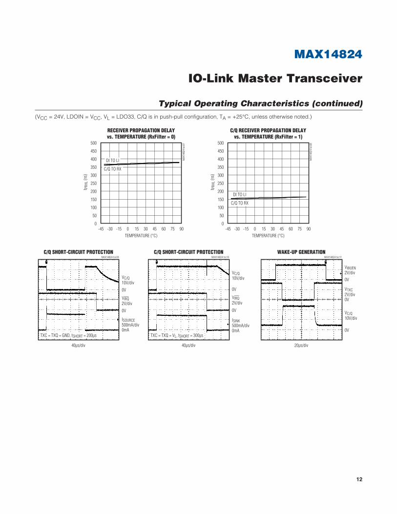
Typical Operating Characteristics(VCC = 24V, LDOIN = VCC, VL = LDO33, C/Q is in push-pull configuration, TA = +25NC, unless otherwise noted.)
C/Q DRIVER OUTPUT SWITCHING(HiSlew = 0)
MAX14824 toc05
2µs/div
VC/Q5V/div
VTXC2V/div
0V
0V
Ch1 Ch21.593µs
Ch1 Ch21.408µs
Ch2 RISE1.618µs
Ch2 FALL1.520µs
TXEN = VLTXC = TXQ
C/Q DRIVER OUTPUT SWITCHING(HiSlew = 1)
MAX14824 toc06
2µs/div
VC/Q5V/div
VTXC2V/div
0V
0V
Ch1 Ch2425.9ns
Ch1 Ch2381.9ns
Ch2 RISE365.6ns
Ch2 FALL370.4ns
TXEN = VLTXC = TXQ
C/Q DRIVER PROPAGATION DELAYvs. TEMPERATURE (HiSlew = 1)
MAX
1482
4 to
c04
TEMPERATURE (°C)
t PDH
L (µ
s)
60 754530150-15-30
0.20
0.25
0.30
0.35
0.40
0.45
0.50
0.15-45 90
TXEN = VLTXC = TXQ
C/Q DRIVER PROPAGATION DELAYvs. TEMPERATURE (HiSlew = 0)
MAX
1482
4 to
c03
TEMPERATURE (°C)
t PDH
L (µ
s)
756030 45-15 0 15-30
1.32
1.34
1.36
1.38
1.40
1.42
1.44
1.46
1.48
1.50
1.30-45 90
TXEN = VLTXC = TXQ
C/Q DRIVER OUTPUT LOWvs. LOAD CURRENT
MAX
1482
4 to
c02
LOAD CURRENT (mA)
V OL_
C/Q
(V)
700600500400300200100
1
2
3
4
5
6
7
00 800
TA = +25°C
TA = +85°C
TA = +105°C
TA = -40°C
TXEN = VLTCX = TXQ = VL
C/Q DRIVER OUTPUT HIGHvs. LOAD CURRENT
MAX
1482
4 to
c01
LOAD CURRENT (mA)
V OH_
C/Q
(V)
700600500400300200100
18
19
20
21
22
23
24
170 800
TA = +25°C
TA = +85°C
TA = +105°C
TA = -40°C
TXEN = VLTCX = TXQ = GND
12
MAX14824
IO-Link Master Transceiver
Typical Operating Characteristics (continued)(VCC = 24V, LDOIN = VCC, VL = LDO33, C/Q is in push-pull configuration, TA = +25NC, unless otherwise noted.)
WAKE-UP GENERATIONMAX14824 toc11
20µs/div
VC/Q10V/div
VTXC2V/div0V
0V
0V
VWUEN2V/div
C/Q SHORT-CIRCUIT PROTECTIONMAX14824 toc10
40µs/div
ISINK500mA/div
VC/Q10V/div
0V
0mA
0V
VIRQ2V/div
TXC = TXQ = VL, tSHORT = 300µs
C/Q SHORT-CIRCUIT PROTECTIONMAX14824 toc09
40µs/div
ISOURCE500mA/div
TXC = TXQ = GND, tSHORT = 200µs
VC/Q10V/div
0V
0mA
0V
VIRQ2V/div
C/Q RECEIVER PROPAGATION DELAYvs. TEMPERATURE (RxFilter = 1)
MAX
1482
4 to
c08
TEMPERATURE (°C)
t PRH
L (n
s)
756030 45-15 0 15-30
50
100
150
200
250
300
350
400
450
500
0-45 90
DI TO LI
C/Q TO RX
RECEIVER PROPAGATION DELAYvs. TEMPERATURE (RxFilter = 0)
MAX
1482
4 to
c07
TEMPERATURE (°C)
t PRH
L (n
s)
756030 45-15 0 15-30
50
100
150
200
250
300
350
400
450
500
0-45 90
DI TO LI
C/Q TO RX

13
MAX14824
IO-Link Master Transceiver
Typical Operating Characteristics (continued)(VCC = 24V, LDOIN = VCC, VL = LDO33, C/Q is in push-pull configuration, TA = +25NC, unless otherwise noted.)
LDOIN SUPPLY CURRENTvs. LDOIN VOLTAGE
MAX
1482
4 to
c15
VLDOIN (V)
I LDO
IN (m
A)
30 33272421181512
0.5
1.0
1.5
2.0
2.5
3.0
3.5
09 36
TA = +85°C TA = +25°C
TA = -40°C
VCC = 36VC/Q DRIVER IS ENABLEDTXC = TXQ = VL
VCC SUPPLY CURRENTvs. C/Q DATA RATE
MAX
1482
4 to
c16
C/Q DATA RATE (kbps)
I CC
(mA)
10010
2
4
6
8
10
12
14
16
18
20
01 1000
VLDOIN = V5 = 5V, TXEN = VL,HiSlew = 1, NO LOAD ON C/Q,CONTINUOUS 1010 PATTERN TRANSMISSION
VCC = 36V
VCC = 30V
VCC = 24V
VCC SUPPLY CURRENTvs. VCC VOLTAGE
MAX
1482
4 to
c14
VCC VOLTAGE (V)
I CC
(mA)
333024 2715 18 2112
0.2
0.4
0.6
0.8
1.0
1.2
1.4
1.6
1.8
2.0
09 36
TA = +85°C
TA = +25°CTA = -40°C
VLDOIN = 7VC/Q DRIVER IS ENABLEDTXC = TXQ = VL
LDO33 LOAD REGULATION
MAX
1482
4 to
c13
LOAD CURRENT (mA)
% V
OLTA
GE C
HANG
E
454030 3510 15 20 255
-0.9
-0.8
-0.7
-0.6
-0.5
-0.4
-0.3
-0.2
-0.1
0
-1.00 50
TA = +25°C
TA = +85°C
TA = -40°C
V5 LOAD REGULATION
MAX
1482
4 to
c12
LOAD CURRENT (mA)
% V
OLTA
GE C
HANG
E
40302010
-0.4
-0.3
-0.2
-0.1
0
0.1
-0.50 50
TA = +25°C
TA = +85°C
TA = -40°C

14
MAX14824
IO-Link Master Transceiver
Pin Configuration
Pin Description
PIN NAME FUNCTION
1 LDOIN 5V Linear-Regulator Input. Bypass LDOIN to GND with a 0.1FF ceramic capacitor.
2 V55V Power-Supply Input and 5V Linear-Regulator Output. Bypass V5 to GND with a 0.1FF ceramic capacitor. See the 5V and 3.3V Linear Regulators section for more information.
3 LDO33 3.3V Linear-Regulator Output. Bypass LDO33 to GND with a 1FF ceramic capacitor.
4 IRQ Active-Low Interrupt Request Output. IRQ is a push-pull output referenced to VL.
5 SCLK SPI Clock Input
6 CS SPI Chip-Select Input
7 SDO SPI Serial-Data Output Port
8 SDI SPI Serial-Data Input Port
9 VLLogic-Level Supply Input. VL defines the logic levels on all the logic inputs and outputs. Bypass VL to GND with a 0.1FF ceramic capacitor.
10 A3 Chip-Select Address Input 3. Do not leave A3 unconnected.
11 TXQ Transmit Level Input. TXQ is ANDed with TXC. Drive TXQ high if not in use.
12 TXC Transmit Communication Input. TXC is ANDed with TXQ. Drive TXC high if not in use.
13 TXENTransmitter Enable. Driving TXEN high enables the C/Q transmitter. While the C/Q transmitter is enabled, the C/Q current sink is turned off.
23
24
22
21
8
7
9
V 5 IRQ
SCLK CS
10
LDOI
N
LI WUE
N
RXUV TXEN
1 2
A1
4 5 6
1718 16 14 13
VCC
A0
A3
VL
SDI
SDO
*EP
*CONNECT EXPOSED PAD TO GND.
LDO3
3A2
3
15
C/Q
20 11 TXQGND
19 12 TXCDI
TQFN(4mm × 4mm)
TOP VIEW
+
MAX14824
15
MAX14824
IO-Link Master Transceiver
Pin Description (continued)
Detailed Description
The MAX14824 is an IO-LinkM master transceiver that integrates an IO-Link physical interface with an additional 24V digital input and two LDOs. A 12MHz SPIK interface allows fast programming and monitoring.
The device supports COM1, COM2, and COM3 IO-Link data rates and has the option of limiting emitted EMI by selecting a lower slew rate at lower data rates. The auto-matic wake-up circuitry determines the correct wake-up pulse polarity, allowing the use of simple UARTs for wake-up pulse generation.
The C/Q and DI inputs have selectable current sinks that can be enabled for use in actuators.
The device is configured and monitored through an SPI interface. Extensive alarms are available through SPI.
24V InterfaceThe device features an IO-Link transceiver interface capable of operating with voltages up to 36V. This includes the C/Q input/output and the logic-level digital input (DI).
DI is reverse-polarity protected. Short-circuit protection is provided on the C/Q driver.
Configurable C/Q DriverThe device’s C/Q driver has a selectable push-pull, high-side (PNP), or low-side (NPN) switching driver.
Set the C/Q_N/P and C/Q_PP bits in the CQConfig reg-ister to select the driver mode for the C/Q driver. When configured as a push-pull output, C/Q switches between VCC and ground. Set the C/Q_PP bit to 1 to select push-pull operation. Set the C/Q_PP bit to 0 to configure the C/Q output for open-drain operation. The C/Q_N/P bit selects NPN or PNP operation when C/Q is configured as an open-drain output.
C/Q Driver and ReceiverThe C/Q driver can be enabled through hardware (TXEN) or software (C/QDEn). Drive TXEN high to enable the C/Q driver and drive TXEN low to disable the driver. The C/Q driver can be enabled through the C/QDEn bit in the C/QConfig register.
The C/Q driver on the device is specified for 300mA to drive large capacitive loads over 1FF and dynamic impedances like incandescent lamps.
IO-Link is a registered trademark of Procibus User Organization (PNO).
SPI is a trademark of Motorola Inc.
PIN NAME FUNCTION
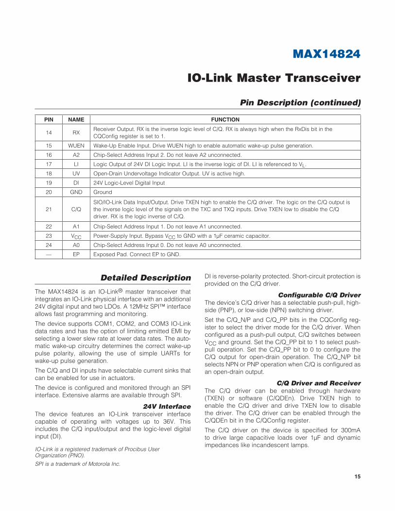
14 RXReceiver Output. RX is the inverse logic level of C/Q. RX is always high when the RxDis bit in the CQConfig register is set to 1.
15 WUEN Wake-Up Enable Input. Drive WUEN high to enable automatic wake-up pulse generation.
16 A2 Chip-Select Address Input 2. Do not leave A2 unconnected.
17 LI Logic Output of 24V DI Logic Input. LI is the inverse logic of DI. LI is referenced to VL.
18 UV Open-Drain Undervoltage Indicator Output. UV is active high.
19 DI 24V Logic-Level Digital Input
20 GND Ground
21 C/QSIO/IO-Link Data Input/Output. Drive TXEN high to enable the C/Q driver. The logic on the C/Q output is the inverse logic level of the signals on the TXC and TXQ inputs. Drive TXEN low to disable the C/Q driver. RX is the logic inverse of C/Q.
22 A1 Chip-Select Address Input 1. Do not leave A1 unconnected.
23 VCC Power-Supply Input. Bypass VCC to GND with a 1FF ceramic capacitor.
24 A0 Chip-Select Address Input 0. Do not leave A0 unconnected.
— EP Exposed Pad. Connect EP to GND.

16
MAX14824
IO-Link Master Transceiver
The HiSlew bit increases the slew rate of the C/Q driver output. Set HiSlew to 1 for data rates of 230kbps or higher. Set HiSlew to 0 to reduce the C/Q driver slew rate and reduce EMI emission and reflections.
The C/Q receiver is always on. Disable the RX output through the RxDis bit in the CQConfig register. Set the RxDis bit to 1 to set the RX output high. Set the RxDis bit to 0 for normal receive operation.
The C/Q receiver has an analog lowpass filter to reduce high-frequency noise present on the line. Set the RxFilter bit in the CQConfig register to 0 to set the filter corner frequency to 500kHz (typ). Set the RxFilter bit to 1 to set the corner frequency of the filter to 1MHz (typ). Noise filters are present on both the C/Q and DI receivers and are controlled simultaneously by the RxFilter bit.
C/Q Fault DetectionThe device registers a C/QFault condition under either of two conditions:
1) When it detects a short circuit for longer than 160µs (typ). A short condition exists when the C/Q driver’s load current exceeds the 670mA (typ) current limit.
2) When it detects a voltage level error at the C/Q out-put. A voltage level error occurs when the C/Q driver is configured for open-drain operation (NPN or PNP), the driver is turned off, and the C/Q voltage is not pulled to exceed the C/Q receiver’s threshold levels (< 8V or > 13V) by the external supply.
When a C/QFault error occurs, the C/QFault and C/QFaultInt bits are set, IRQ asserts, and the driver is turned off 240µs (typ) after the start of the fault condition.
When a short-circuit event occurs on C/Q, the driver enters autoretry mode. In autoretry mode the device peri-odically checks if the short is still present and attempts to correct the driver output. Autoretry attempts last for 350µs (typ) and occur every 26ms (typ).
DI Auxillary Digital InputDI is a digital input that is Type 1 and Type 3 compliant when the internal 3.5mA DI current load is enabled. If the IO-link master system does not require auxilliary digital inputs, DI can be connected to C/Q as shown in the Typical Operating Circuits. This reduces the power dissi-pation when C/Q is operated as a digital input, by enabling the DI current load instead of the C/Q current load. Di is tolerant to reverse polarity voltages down to -40V when not connected to C/Q.
5V and 3.3V Internal RegulatorsThe device includes two internal current-limited regulators to generate 5V (V5) and 3.3V (LDO33). V5 is specified at 10mA. LDO33 is specified at 10mA. The input of V5, LDOIN, can be connected to VCC or to another voltage in the 7V to 36V range.
V5 consitutes the supply for the logic block in the device. The device can be powered by an external 5V power supply. Disable the 5V LDO by connecting LDOIN to V5. Apply an external voltage from 4.75V to 5.25V to V5 when the LDO is disabled.
Use the LDO33Dis bit in the Mode register to enable/disable LDO33. See the Mode Register [R1, R0] = [1,1] section for more information. V5 and LDO33 are not pro-tected against short circuits.
Power-UpThe C/Q driver output and the UV output are high imped-ance when VCC, V5, VL, and/or LDO33 voltages are below their respective undervoltage thresholds during power-up. UV goes low and the C/Q driver is enabled when all these voltages exceed their respective under-voltage lockout thresholds.
The C/Q driver is automatically disabled if VCC, V5, or VL falls below its threshold.
Undervoltage DetectionThe device monitors VCC, V5, VL, and, optionally, LDO33 for undervoltage conditions. UV is high impedance when any monitored voltage falls below its UVLO threshold.
VCC, V5, and VL undervoltage detection cannot be dis-abled. When VCC falls below the VCCUVLO threshold, the UV24 and UV24Int bits are set, UV asserts high, and IRQ asserts low.
The SPI register contents are unchanged while V5 is present, regardless of the state of VCC or LDO33. The SPI interface is not accessible and IRQ is not available when UV is asserted due to a V5 or VL undervoltage event.
When the internal 3.3V LDO regulator voltage (VLDO33) falls below the LDO33 undervoltage lockout threshold, the UV33Int bit in the Status register is set and IRQ asserts. UV asserts if the UV33En bit in the Mode register is set to 1.
The UV output deasserts once the undervoltage condi-tion is removed; however, the associated interrupts bits in the Status register and the IRQ output are not cleared until the Status register has been read.

17
MAX14824
IO-Link Master Transceiver
Wake-Up GenerationThe MAX14824 features automatic wake-up polarity gen-eration functionality that can be initiated through hard-ware or software. The following conditions must be met prior to automatic wake-up polarity generation to ensure proper functionality:
• WUENislow
• TXENislowandC/QDEn=0
• Q=0
• TXCandTXQarebothhigh
Drive WUEN high to enable the automatic wake-up polarity generation circuitry in the device. When WUEN is high, apply an external pulse to TXC or TXQ from high-to-low for 80Fs (typ) to generate a valid wake-up pulse. The applied pulse is independent of the logic state that the IO-Link sensor was forcing on the C/Q level (Figure 5). Drive WuEN low after the wake-up has been generated.
The C/Q driver is automatically enabled while TXC/TXQ is low and C/Q is pulled either from high-to-low or from low-to-high, depending on the previous state. The C/Q driver is automatically disabled when the TXC/TXQ inputs are pulled high again.
Wake-up polarity generation can also be enabled through software by setting the WuEnBit bit in the Mode register to 1. See the Mode Register [R1, R0] = [1,1] section for more information.
Thermal Protection and ConsiderationsThe internal LDOs and C/Q driver can generate more power than the package for the device can safely dis-sipate. Ensure that the driver LDO loading is less than the package can dissipate. Total power dissipation for the device is calculated using the following equation:
PTOTAL = PC/Q + P5 + PLDO33 + PQ + PCLCQ + PCLDI
where PC/Q is the power generated in the C/Q driver, P5 and PLDO33 are the power generated by the LDOs, PQ is the quiescent power generated by the device, and PCLCQ and PCLDI are the power generated in the C/Q and DI current sinks.
Ensure that the total power dissipation is less than the limits listed in the Absolute Maximum Ratings section.
Use the following to calculate the power dissipation (in mW) due to the C/Q driver:
PC/Q = [IC/Q]2 x [RO]
Calculate the power dissipation in the 5V LDO, V5, using the following equation:
P5 = (VLDOIN - V5) × I5where I5 includes the ILDO33 current sourced from LDO33.
Calculate the power dissipated in the 3.3V LDO, LDO33, using the following equation:
PLDO33 = 1.7V × ILDO33
Calculate the quiescent power dissipation in the device using the following equation:
PQ = ICC × VCC
If the current sinks are enabled, calculate their associ-ated power dissipation as:
PCLCQ = ILLM_C/Q × VC/Q
PCLDI = ILLM_DI × VDI
Overtemperature WarningTwo bits in the Status and Mode registers are set when the temperature of the device exceeds +115NC (typ). The OTempInt bit in the Status register is set and IRQ asserts when the OTemp bit in the Mode register is set. Read the Status register to clear the OTempInt bit and IRQ.
The OTemp bit is cleared when the die temperature falls below +95NC.
The device continues to operate normally unless the die temperature reaches the +150NC thermal shutdown threshold, when the device enters thermal shutdown.
Thermal ShutdownWhen the die temperature rises above +150NC (typ) ther-mal shutdown threshold, the C/Q drivers and the C/Q and DI current loads are automatically turned off. The internal 3.3V and 5V LDOs remain on during thermal shutdown, if enabled. If the internal or external V5 supply remains on during thermal shutdown (which is always true in case of the internal V5 regulator), the register contents are main-tained and SPI communication available.
When the die temperature falls below the thermal shut-down threshold plus hysteresis, the C/Q driver and C/Q and DI current sinks turn on automatically.

18
MAX14824
IO-Link Master Transceiver
Register Functionality
The device has four 8-bit-wide registers for configuration and monitoring (Table 1). R1 and R0 are the register address.
Table 1. Register Summary
R1/R0 = Register address, X = Unused bits.
Status Register [R1, R0] = [0,0]
REGISTER R1 R0 D7 D6 D5 D4 D3 D2 D1 D0
Status 0 0 X X DiLvl QLvl C/QFaultInt UV33Int UV24Int OTempInt
CQConfig 0 1 RxFilter HiSlew C/Q_N/P C/Q_PP C/QDEn Q RxDis C/QLoad
DIOConfig 1 0 X X X X X X LiDis DiLoad
Mode 1 1 RST WuEnBit X C/QFault UV24 OTemp UV33En LDO33Dis
Bit D7 D6 D5 D4 D3 D2 D1 D0
Bit Name X X DiLvl QLvl C/QFaultInt UV33Int UV24Int OTempInt
Read/Write R R R R R R R R
POR State 0 0 U U 0 0 0 0
Reset Upon Read Yes Yes No No Yes Yes Yes Yes
X = Unused bits.U = Unknown. These bits are dependent on the DI logic and C/Q inputs.
The Status register reflects the logic levels of C/Q and DI and shows the source of interrupts that cause an IRQ hardware interrupt. The IRQ interrupt is asserted when an alarm condition (OTemp, UV33En, UV24, C/QFault) is detected. All bits in the Status register are read-only. The interrupt bits return to the default state after the Status register is read. If a C/Q fault condition persists, the C/QFaultInt bit is immediately set after the Status register is read.
BIT NAME DESCRIPTION
D7:D6 X Unused
D5 DiLvl DI Logic Level. The DiLvl bit mirrors the current logic level at the DI input. It is the inverse of the LI output and is always active regardless of the state of the LiDis bit (Table 2). DiLvl does not affect IRQ. DiLvl is not changed when the Status register is read.
D4 QLvl C/Q Logic Level. The QLvl bit is the inverse of the logic level at C/Q. QLvl is 1 when the C/Q input level is low (< 8V) and is 0 when the C/Q logic level is high (> 13V) (Table 3). QLvl remains active when the C/Q receiver is disabled (RxDis = 1). QLvl does not affect IRQ. QLvl is not changed when the Status register is read.
D3 C/QFaultInt C/Q Fault Interrupt. The C/QFaultInt interrupt bit and C/QFault bit (in the Mode register) are set when a short circuit or voltage fault occurs on the C/Q driver output (see the C/Q Fault Detection section for more information). IRQ asserts when C/QFault is 1. Read the Status register to clear the C/QFaultInt bit and deassert IRQ.

19
MAX14824
IO-Link Master Transceiver
Table 2. DiLvl and LI Output Table 3. QLvl and RX Output
VDI (V) DiLvl BIT LI OUTPUT
< 5.2 0 High
> 8 1 Low
VC/Q (V) QLvl BIT RX OUTPUT
< 8 1 High
>13 0 Low
BIT NAME DESCRIPTION
D2 UV33Int Internal 3.3V LDO (LDO33) Undervoltage Warning. Both the UV33Int interrupt bit and the UV33En bit (in the Mode register) are set when VLDO33 falls below the 2.4V LDO33 undervoltage threshold. If UV33En is set in the Mode register, IRQ asserts low when the UV33Int bit is 1. Read the Status register to clear the UV33Int bit and deassert IRQ.
Set the UV33En bit to 1 in the Mode register to enable undervoltage monitoring for UV33Int. When enabled, UV asserts high when the UV33Int bit is 1. UV deasserts when VLDO33 rises above the LDO33 undervoltage threshold.
D1 UV24Int VCC Undervoltage Interrupt. The UV24Int interrupt bit and the UV24 bit (in the Mode register) are set when the VCC voltage falls below the 7.4V undervoltage threshold. IRQ asserts low when the UV24Int bit is 1. Read the Status register to clear the UV24Int bit and deassert IRQ. VCC undervoltage detection cannot be disabled.
D0 OTempInt Overtemperature Warning. The OTempInt interrupt bit and the OTemp bit (in the Mode register) are set when a high-temperature condition is detected by the device. OTemp is set when the temperature of the die exceeds +115NC (typ). OTempInt is set and IRQ asserts when the OTemp bit is 1. The OTempInt bit is cleared and IRQ deasserts when the Status register is read.
Once cleared, OTempInt is not reset if the die temperature remains above the thermal warning threshold and does not fall below +95°C.
20
MAX14824
IO-Link Master Transceiver
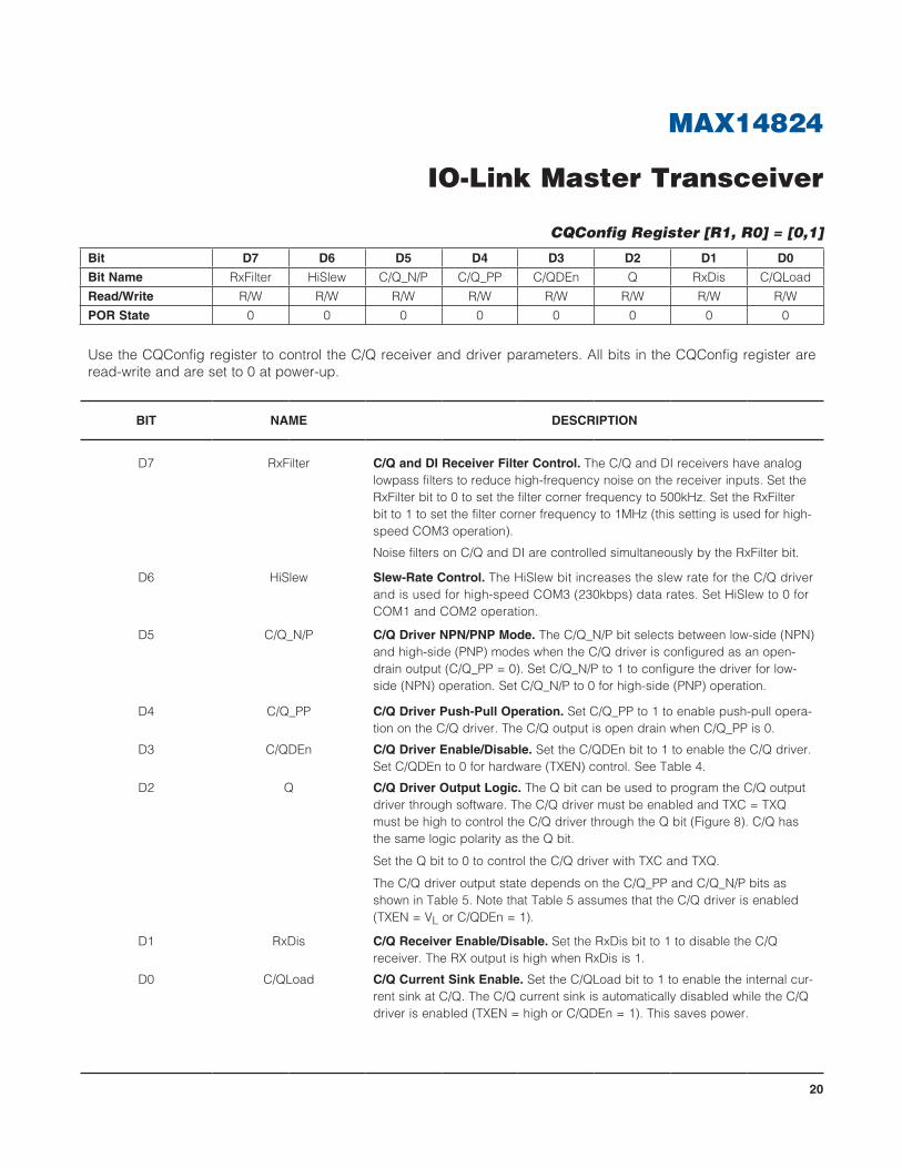
CQConfig Register [R1, R0] = [0,1]
Bit D7 D6 D5 D4 D3 D2 D1 D0
Bit Name RxFilter HiSlew C/Q_N/P C/Q_PP C/QDEn Q RxDis C/QLoad
Read/Write R/W R/W R/W R/W R/W R/W R/W R/W
POR State 0 0 0 0 0 0 0 0
Use the CQConfig register to control the C/Q receiver and driver parameters. All bits in the CQConfig register are read-write and are set to 0 at power-up.
BIT NAME DESCRIPTION
D7 RxFilter C/Q and DI Receiver Filter Control. The C/Q and DI receivers have analog lowpass filters to reduce high-frequency noise on the receiver inputs. Set the RxFilter bit to 0 to set the filter corner frequency to 500kHz. Set the RxFilter bit to 1 to set the filter corner frequency to 1MHz (this setting is used for high-speed COM3 operation).
Noise filters on C/Q and DI are controlled simultaneously by the RxFilter bit.
D6 HiSlew Slew-Rate Control. The HiSlew bit increases the slew rate for the C/Q driver and is used for high-speed COM3 (230kbps) data rates. Set HiSlew to 0 for COM1 and COM2 operation.
D5 C/Q_N/P C/Q Driver NPN/PNP Mode. The C/Q_N/P bit selects between low-side (NPN) and high-side (PNP) modes when the C/Q driver is configured as an open-drain output (C/Q_PP = 0). Set C/Q_N/P to 1 to configure the driver for low-side (NPN) operation. Set C/Q_N/P to 0 for high-side (PNP) operation.
D4 C/Q_PP C/Q Driver Push-Pull Operation. Set C/Q_PP to 1 to enable push-pull opera-tion on the C/Q driver. The C/Q output is open drain when C/Q_PP is 0.
D3 C/QDEn C/Q Driver Enable/Disable. Set the C/QDEn bit to 1 to enable the C/Q driver. Set C/QDEn to 0 for hardware (TXEN) control. See Table 4.
D2 Q C/Q Driver Output Logic. The Q bit can be used to program the C/Q output driver through software. The C/Q driver must be enabled and TXC = TXQ must be high to control the C/Q driver through the Q bit (Figure 8). C/Q has the same logic polarity as the Q bit.
Set the Q bit to 0 to control the C/Q driver with TXC and TXQ.
The C/Q driver output state depends on the C/Q_PP and C/Q_N/P bits as shown in Table 5. Note that Table 5 assumes that the C/Q driver is enabled (TXEN = VL or C/QDEn = 1).
D1 RxDis C/Q Receiver Enable/Disable. Set the RxDis bit to 1 to disable the C/Q receiver. The RX output is high when RxDis is 1.
D0 C/QLoad C/Q Current Sink Enable. Set the C/QLoad bit to 1 to enable the internal cur-rent sink at C/Q. The C/Q current sink is automatically disabled while the C/Q driver is enabled (TXEN = high or C/QDEn = 1). This saves power.

21
MAX14824
IO-Link Master Transceiver
Table 5. C/Q Driver Output State
Note: TXC and TXQ = VL.
X = Don’t care.
Table 4. C/QDEn and TXEN C/Q Driver Control
X = Don’t care.
DIOConfig Register [R1, R0] = [1,0]
Figure 7. Equivalent C/Q Logic
TXC AND TXQ(SEE NOTE)
Q C/Q_PP C/Q_N/P C/Q CONFIGURATION C/Q STATE
High 1 0 0 PNP, open drain On, C/Q is high
High 0 0 0 PNP, open drain Off, C/Q is high impedance
High 1 0 1 NPN, open drain Off, C/Q is high impedance
High 0 0 1 NPN, open drain On, C/Q is low
High 1 1 X Push-pull High
High 0 1 X Push-pull Low
C/QDEn TXEN C/Q DRIVER
0 Low Disabled
X High Enabled
1 X Enabled
Bit D7 D6 D5 D4 D3 D2 D1 D0
Bit Name X X X X X X LiDis DiLoad
Read/Write R/W R/W R/W R/W R/W R/W R/W R/W
POR State 0 0 0 0 0 0 0 0
X = Unused bits.
Use the DIOConfig register to control the DI and DO interfaces. All bits in the DIOConfig register are read-write and are set to 0 at power-up.
BIT NAME DESCRIPTION
D7:D2 X Unused
D1 LiDis LI Output Enable/Disable. Set the LiDis bit to 1 to disable the LI output. The LI output is low when LiDis is 1.
D0 DiLoad DI Current Sink Enable. Set the DiLoad bit to 1 to enable the internal current sink at the DI input.
TXQC/QTXC
Q

22
MAX14824
IO-Link Master Transceiver
Mode Register [R1, R0] = [1,1]
Bit D7 D6 D5 D4 D3 D2 D1 D0
Bit Name RST WuEnBit X C/QFault UV24 OTemp UV33En LDO33Dis
Read/Write R/W R/W R/W R R R R/W R/W
POR State 0 0 0 0 0 0 0 0
X = Unused bits.
Use the Mode register to reset the device and manage the 3.3V LDO. The Mode register has bits that represent the current status of fault conditions. When writing to the Mode register, the contents of the fault indication bits (bits 2 to 4) do not change.
BIT NAME DESCRIPTION
D7 RST Register Reset. Set RST to 1 to reset all registers to their default power-up state. Then set RST to 0 for normal operation.
The Status register is cleared and IRQ deasserts (if asserted) when RST = 1. Interrupts are not generated while RST = 1.
D6 WuEnBit Auto Wake-Up Polarity Enable. Drive the WUEN input high or set the WuEnBit bit to 1 to enable wake-up generation. When auto wake-up polarity is enabled, the device sam-ples the logic state of C/Q and uses this as the basis for determining the subsequent wake-up pulse that is initiated through a high-to-low pulse on the TXQ and TXC inputs.
Set the WuEnBit to 1 before a negative-going, 80µs (typ) wake-up pulse is transmitted to ensure that the device produces the correct polarity wake-up pulse on the C/Q output. For example, if C/Q is connected to a voltage high, then it pulls the line low for the wake-up pulse duration. If C/Q is connected to a voltage low, then it pulls the line high for the wake-up pulse duration. Clear WuEnBit after the wake-up has been generated (Table 6).
D5 X Unused
D4 C/QFault C/Q Fault Status. The C/QFault bit is set when a short circuit or voltage fault occurs at the C/Q driver output (see the C/Q Fault Detection section for more information). The C/QFault and C/QFaultInt bits are both set when a fault occurs on C/Q. C/QFault is cleared when the fault is removed.
D3 UV24 VCC Undervoltage Condition. Both the UV24 and the UV24Int bits are set when VCC falls below VCCUVLO. UV24 is cleared when VCC rises above the VCC threshold. V5 must be present for VCC undervoltage monitoring.
D2 OTemp Temperature Warning. The OTemp bit is set when a high-temperature condition occurs on the device. Both the OTempInt interrupt in the Status register and the OTemp bit are set when the junction temperature of the die rises to above +115NC (typ). The OTemp bit is cleared when the junction temperature falls below +95NC (typ).
D1 UV33En LDO33 UV Enable. Set the UV33En bit to 1 to assert the UV output when LDO33 volt-age falls below the 2.4V (typ) undervoltage lockout threshold. The UV33En bit does not affect the UV33Int bit in the Status register; IRQ asserts when VLDO33 falls below VLDO33UVLO regardless of the state of UV33En.
D0 LDO33Dis LDO33 Enable/Disable. Set LDO33Dis to 1 to disable the 3.3V linear regulator (LDO33).

23
MAX14824
IO-Link Master Transceiver
Figure 8. SPI Write Cycle
Figure 9. SPI Read Cycle
SPI InterfaceThe device communicates through an SPI-compatible 4-wire serial interface. The interface has three inputs— clock (SCLK), chip select (CS), and data in (SDI)—and one output, data out (SDO). The maximum SPI clock rate
for the device is 12MHz. The SPI interface complies with clock polarity CPOL = 0 and clock phase CPHA = 0 (see Figure 8 and Figure 9).
The SPI interface is not available when V5 or VL is not present.
Table 6. Auto Wake-Up Polarity GenerationWuEnBit WUEN MODE
0 Low Normal operation
0 High Wake-up generation mode
1 Low Wake-up generation mode
1 High Wake-up generation mode
R0 D7 D6 D5 D4 D3 D2 D1 D0
SCLK
A_ = DEVICE ADDRESSR_ = REGISTER ADDRESSD_ = DATA BIT
= CLOCK EDGE WHEN LOGIC IS LATCHED
SDI W 0 A3 A2 A1 A0 R1
CS
SCLK
R1 R0A3 A2 A1 A0
CS
D7 D6 D5 D4 D3 D2 D1 D0
A_ = DEVICE ADDRESSR_ = REGISTER ADDRESSD_ = DATA BIT
= CLOCK EDGE WHEN LOGIC IS LATCHED
= CLOCK EDGE AT WHICH LOGIC IS WRITTEN
SDI 0R
SDO
XX

24
MAX14824
IO-Link Master Transceiver
Address SelectionThe device includes four chip-select address inputs, A0–A3, allowing up to 16 devices on a single bus. Drive the address inputs high or low to program the device address as shown in Table 7. Do not leave any address input unconnected.
Applications Information
UART InterfacingThe logic level of the MAX14824 microcontroller’s UART interface I/Os (TXC, TXQ, TXEN, and RX) is defined by VL.
The device can be interfaced to microcontrollers whose on-board UART TX output cannot be programmed as a logic output (GPO). In this case, connect the TX output of the UART to the TXC input for IO-Link communication and connect a separate GPO output on the microcon-troller to TXQ for standard IO (SIO) mode operation (Figure 10). As the TXQ and TXC inputs are internally logically ANDed, the unused input (TXC or TXQ) must be held high while the other is in operation.
Transient ProtectionInductive load switching, surges, ESD and short circuits create high transient voltages. C/Q and DI must be pro-tected against high overvoltage and undervoltage tran-sients. Positive voltage transients on DI must be limited to +55V relative to GND and negative voltage transients must be limited to -55V (relative to GND) on DI. Two Schottky diodes having low forward voltage, like the DLFS240, must be connected to C/Q to clamp under- and overvoltage transients. Figure 11 shows suitable protection to meet IEC 61000-4-2 ESD testing. For reduction of bit errors induced by burst transients, enable the receiver filters and add capacitors to C/Q and DI. If surge tests need to be met, a TVS diode is recommended on VCC.
Figure 10. UART Interface
Figure 11. MAX14824 Operating Circuit with TVS Protection
Table 7. Address Input SelectionA3 A2 A1 A0 DEVICE ADDRESS
Low Low Low Low 0x00
Low Low Low High 0x01
Low Low High Low 0x02
Low Low High High 0x03
Low High Low Low 0x04
Low High Low High 0x05
Low High High Low 0x06
Low High High High 0x07
High Low Low Low 0x08
High Low Low High 0x09
High Low High Low 0x0A
High Low High High 0x0B
High High Low Low 0x0C
High High Low High 0x0D
High High High Low 0x0E
High High High High 0x0F
MIC
ROCO
NTRO
LLER TXQGPO
TXCTX
TXENRTS
RXRX
MAX14824
MAX14824
1nF
270pF
VCC
C/Q
DFLS240
SDC36C
1µF
270pF
GND
DI
DFLS240

25
MAX14824
IO-Link Master Transceiver
External PowerThe device is powered by VCC and the 5V regulator, V5. VL is a reference voltage input to set the logic levels of the microcontroller interface. The logic and SPI interface are operational when V5 and VL are present even if VCC is not present.
Connect LDOIN to V5 to power the V5 input with an external supply (Figure 12). This configuration disables operation of the internal 5V regulator and reduces power consumption.
Figure 12. Use an External Supply to Power the MAX14824
12
43
10kΩ
MAX14824
MAX17501
1μF 1μF
VCCUVGPIO2LDOIN
C/Q
LX
FBGND
SPI
INEN
DI
L+
L-
GNDGND
V5VCC LDO33VL TXQ
MICROCONTROLLERWUENGPIO1
RXRX
TXCTX
TXENRTS
LIGPIO3
3.3V
1nF
270pF
270pF

26
MAX14824
IO-Link Master Transceiver
Typical Operating Circuits (continued)
TXEN
ADDR 1
TXC
MAX14824
RX
PORT 1
MISO
MOSI
SCLK
CS1
CS2
RST
CONTROLLER
MAX14824
PORT 3
MAX14824
PORT 1
MAX14824
RX
PORT 2
TXEN
ADDR 2
TXC
RX
TXEN
ADDR 3
TXC
RX
TXEN
ADDR 4
TXC
MAX14830
GPIO1
GPIO9
GPIO13
IO-LINK QUAD MASTER APPLICATION
GPIO5
TX0
RTS0RX0
TX1
RTS1RX1
TX2
RTS2RX2
TX3
RTS3
XOUTXIN
MISOMOSISCLKCSRST
RX3
VEXT

27
MAX14824
IO-Link Master Transceiver
Ordering Information
Chip Information
PROCESS: BiCMOS
Package Information
For the latest package outline information and land patterns (footprints), go to www.maxim-ic.com/packages. Note that a “+”, “#”, or “-” in the package code indicates RoHS status only. Package drawings may show a different suffix character, but the drawing pertains to the package regardless of RoHS status.
+Denotes a lead(Pb)-free/RoHS-compliant package.*EP = Exposed pad.
PART TEMP RANGE PIN-PACKAGE
MAX14824GTG+ -40NC to +105NC 24 TQFN-EP*
PACKAGE TYPE
PACKAGE CODE
OUTLINE NO.
LAND PATTERN NO.
24 TQFN-EP T2444+4 21-0139 90-0022

MAX14824
IO-Link Master Transceiver
Maxim cannot assume responsibility for use of any circuitry other than circuitry entirely embodied in a Maxim product. No circuit patent licenses are implied. Maxim reserves the right to change the circuitry and specifications without notice at any time. The parametric values (min and max limits) shown in the Electrical Characteristics table are guaranteed. Other parametric values quoted in this data sheet are provided for guidance.
Maxim Integrated Products, 120 San Gabriel Drive, Sunnyvale, CA 94086 408-737-7600 28
© 2012 Maxim Integrated Products Maxim is a registered trademark of Maxim Integrated Products, Inc.
Revision History
REVISIONNUMBER
REVISIONDATE
DESCRIPTIONPAGES
CHANGED
0 3/11 Initial release —
1 6/11Changed DI threshold to accommodate all three types of industrial sensors, added 24V supply connection in Figure 13
4, 19, 25
2 8/11
Corrected IO-Link trademark. Corrected block description in Functional Diagram. Corrected C/Q minimum and maximum ratings in the Absolute Maximum Ratings section. Corrected ICC maximum value and shuffled row parameters in the Electrical Characteristics Table. Replaced Figures 9 and 10. Added Maxim part number for DC-DC regulator. Corrected Transient Protection section.
1, 2, 3, 23, 24
3 5/12
Changed temperature rating; updated Typical Operating Circuits, Functional Diagram, and Figures 9, 11, and 12; updated TOCs 1, 2, and 16; changed parameters in Electrical Characteristics; updated Detailed Description and Application Information
1-7, 11, 13-17, 20, 23, 24, 24,
25, 27