Embed Size (px)
Citation preview

CDB43L36
Copyright Cirrus Logic, Inc. 2015–2016
Evaluation Board for the CS43L36
Features• Analog I/O uses four-conductor, 1/8” (3.5 mm) audio with
presence detection
• Configurable serial audio headers
• Headphone output from the CS43L36
• S/PDIF Rx/Tx into CS43L36
• FlexGUI software control from USB mini-B— Windows® compatible— Predefined and user-configurable scripts
DescriptionThe CDB43L36 is a dedicated platform for testing and evaluating the CS43L36, a high-performance audio DAC with Class H headphone drivers. To allow comprehensive testing of CS43L36 features and performance, extensive software-configurable options are available on the CDB43L36.
Software options, such as register settings for the CS43L36, are configured via FlexGUI software, which communicates with the CDB43L36 via USB from a Windows-compatible computer.
The CDB43L36 also serves as the component and layout reference for the CS43L36.
Ordering Information
CDB43L36 Evaluation Board
ET-FLEXLINK Daughter card
CS43L36
SCL/SDA
HPSENSA/BHPOUTBHPOUTA
HS3HS3_REF
HEADSET Jack
_____WAKE______RESET___INT
ASP_LRCK/FSYNCASP_SCLKASP_SDIN
TIP_SENSE
SCLKLRCKSDINSDOUT
SCL/SDA
_____WAKE______RESET___INT
CS8422S/PDIF RX
CS8406S/PDIF TX
C8051F320USB MCU
Optical S/PDIF TX
Optical S/PDIF RX
USB 2.0Mini B
+5Vin
Note: Not all signals are shown.
(All Rights Reserved)http://www.cirrus.com
DS1081DB3 MAY ‘16

CDB43L36
Table of Contents1 CDB43L36 System Overview ....................................................................................................................................... 3
1.1 Power-Supply Circuitry .......................................................................................................................................... 41.2 Serial Audio I/O Headers ....................................................................................................................................... 41.3 Headset Jack ......................................................................................................................................................... 41.4 LEDs ...................................................................................................................................................................... 51.5 S/PDIF RX ............................................................................................................................................................. 6
2 Quick Setup Guide ........................................................................................................................................................ 72.1 Quick Setup Guide—FlexGUI Mode with S/PDIF RX ............................................................................................ 72.2 Quick Setup Guide—FlexGUI Mode with External I2S .......................................................................................... 8
3 Software Control Using FlexGUI ................................................................................................................................. 93.1 Working with Register Settings .............................................................................................................................. 93.2 Using the FlexGUI High-Level Interface Layout .................................................................................................. 103.3 The Register Map ................................................................................................................................................ 11
4 System Connections and Jumper Settings .............................................................................................................. 134.1 ASP Selection Jumper Block ............................................................................................................................... 144.2 Headset Load Header ......................................................................................................................................... 14
5 CDB43L36 Schematics and Layout ........................................................................................................................... 156 Revision History ......................................................................................................................................................... 16
2 DS1081DB3

CDB43L361 CDB43L36 System Overview
1 CDB43L36 System Overview
The CDB43L36 evaluation board is a convenient platform for evaluating the CS43L36, a high-fidelity audio DAC with Class H headphone drivers. By default, it is a slave device. However, it can be configured as a hybrid-master device via I2C. It supports multiple power supply and signal I/O configurations and serves as the component and layout reference for the CS43L36.
The following subsections describe the CDB43L36 evaluation board in detail. Fig. 1-1 shows a detailed view of the system.
Figure 1-1. CDB43L36 Block Diagram
ET-FLEXLINK Daughter card
CS43L36
SCL/SDA
HPSENSA/BHPOUTBHPOUTA
HS3HS3_REF
HEADSET Jack
_____WAKE______RESET___INT
ASP_LRCK/FSYNCASP_SCLKASP_SDIN
TIP_SENSE
SCLKLRCKSDINSDOUT
SCL/SDA
_____WAKE______RESET___INT
CS8422S/PDIF RX
CS8406S/PDIF TX
C8051F320USB MCU
Optical S/PDIF TX
Optical S/PDIF RX
USB 2.0Mini B
+5Vin
Note: Not all signals are shown.
DS1081DB3 3

CDB43L361.1 Power-Supply Circuitry
1.1 Power-Supply Circuitry
The CDB43L36 can be powered from a +5-V wall-wart DC power jack (see entry for J4 in Table 4-1).
Low-dropout regulators step down the +5-V supply to provide a clean and stable +1.2-V (x2), +1.8-V, and +3.3-V rails to the CS43L36 and peripheral circuits on the board. This includes a 1.8-V LDO, a 3.3-V LDO, and two 1.2-V LDOs. The 1.2-V LDOs provide a way to externally power up the VD_FILT power pin while supplying 1.2 V for VL. Fig. 1-2 shows the CDB43L36 power routing and configurations.
Figure 1-2. CDB43L36 Power Supplies
1.2 Serial Audio I/O Headers
The ASP HEADER (J68) provides the ability to connect an external audio source or the USB Audio module directly to the CS43L36 ASP. The header signals are described in Table 1-1.The default logic level is 1.8 V.
1.3 Headset Jack
The CDB43L36 platform contains 1-1/8” TRRS jack for headset connection. The jack connects to the HPOUTA, HPOUTB, TIP_SENSE, HS3, and HS3_REF signals on the CS43L36. There is also a headset load header (J2) that can be used to connect an external load when performance measurements are taken.
Table 1-1. Serial Audio I/O Header (J68)
Pin Header Pin Direction Description1 SCLK I/O ET-FLEXLINK SCLK4 LRCK I/O ET-FLEXLINK LRCLK7 SDIN O ET-FLEXLINK SDIN
10 SDOUT O ET-FLEXLINK SDOUT2 CS43L36_SCLK I L36 ASP_SCLK5 CS43L36_LRCK I/O L36 ASP_LRCLK8 NC — —11 CS43L36_SDIN I L36 ASP_SDIN
3, 6, 9, 12 Ground Ground reference Board ground
Board SuppliesCodec Supplies
+3.3-V CDB (Board Power)
+1.8-V Regulator+5-V Wall
+3.3-V CDB+1.2-V LDO
+3.3-V Regulator
VP
+1.2-V LDO
0 Ω
VPVA
0 Ω
VA
VCP
0 Ω
VCP
VL VD_FILT
0 Ω
0 Ω
Note: 0-resistor to +1.2-V LDO is NO POP by default
0 Ω VL_SEL
0 Ω
0 Ω
Note: 0- resistor to GND is NO POP by default
Note: 0-resistor is NO POP by default
____________DIGLDO_PDN
0 Ω
0 Ω
Note: 0- resistor to GND is NO POP by default
VP
4 DS1081DB3

CDB43L361.4 LEDs
1.4 LEDs
There are LED indicators showing the state of the serial buses and GPIO signals—green for Logic 1 and red for Logic 0. In addition, several green LEDs indicate whether respective power supplies are present.The ET-FLEXLINK LEDs are shown in Table 1-2 below. CDB43L36 LEDs are shown in Table 1-2 below.
Table 1-2. ET-FLEXLINK LEDs
LED Color Silkscreen DescriptionD0D1D2D3
Orange D0D1D2D3
MCU outputs, not used by FlexGUI
D4 Green +5V Illuminated when +5V rail is presentD5 Green USB.VBUS Illuminated when USB (J2) VBUS is presentD6 Green +5V.CDB Illuminated when +5V.CDB rail is presentD7 Green +3.3V Illuminated when +3.3V rail is presentD8 Green +1.8V Illuminated when +1.8V rail is presentD9 Green +VIO Illuminated when +VIO rail is present
Table 1-3. CDB43L36 LEDs
LED Color Silkscreen DescriptionD2 Green VP Illuminated when +5V_CDB rail is presentD3 Green +3.3V Illuminated when +3.3V_CDB rail is presentD4 Green +1.8V Illuminated when +1.8V_CDB rail is present
D5/D6 Green/Red H/L INT Green/Red when INT is high/low
D7/D8 Green/Red H/L RESET Green/Red when RESET is high/lowD9/D10 Green/Red H/L SCL Green/Red when SCL is high/lowD11/D12 Green/Red H/L SDA Green/Red when SDA is high/lowD13/D14 Green/Red H/L WAKE Green/Red when WAKE is high/low
DS1081DB3 5
CDB43L361.5 S/PDIF RX
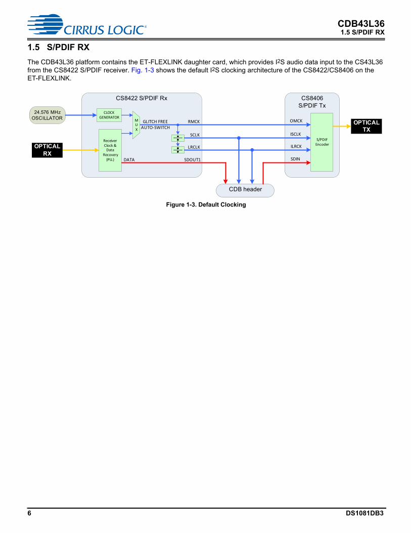
1.5 S/PDIF RX
The CDB43L36 platform contains the ET-FLEXLINK daughter card, which provides I2S audio data input to the CS43L36 from the CS8422 S/PDIF receiver. Fig. 1-3 shows the default I2S clocking architecture of the CS8422/CS8406 on the ET-FLEXLINK.
Figure 1-3. Default Clocking
CS8422 S/PDIF Rx
SDOUT1
CLOCKGENERATOR
24.576 MHz OSCILLATOR
Receiver Clock & Data
Recovery (PLL) DATA
GLITCH FREE AUTO‐SWITCH
RMCK
SCLK
LRCLKOPTICALRX
CDB header
CS8406S/PDIF Tx
S/PDIF Encoder
SDIN
OMCK
ISCLK
ILRCK
MUX
OPTICALTX
6 DS1081DB3

CDB43L362 Quick Setup Guide
2 Quick Setup Guide
The CDB43L36 can be configured in FlexGUI Mode with S/PDIF RX or FlexGUI Mode with external I2S/TDM, or as described in the following section.
2.1 Quick Setup Guide—FlexGUI Mode with S/PDIF RX
This short procedure sets the CDB43L36 to a standard state for evaluation in FlexGUI Mode with S/PDIF RX.
1. Install the FlexGUI software. See Section 3.
2. Set CDB43L36 jumpers ASP header (J68) and J2 and ET-FLEXLINK J3, shown by red indicators in Fig. 2-1. SeeTable 4-1.
3. Connect cabling to the CDB43L36 as shown by green indicators in Fig. 2-1.
4. Launch FlexGUI software (Start Programs Cirrus Logic FlexLoader Launch FlexLoader.exe) and runthe Quick Setup selection based on your desired sample rate. See Section 3.1.2.
Figure 2-1. Jumper Settings and Cabling (FlexGUI Mode with S/PDIF RX)
+5VDC power supply
Windows PCMini‐B
USB Cable
Toslink Digital Optical S/PDIF Audio
Cable
RX
TX
TRS to RCA cable
BNC to RCA
J3.1
+5V
J3.3
CDB
J68.1
SCLKJ68.2
J68.4
LRCKJ68.5
J68.10
SDINJ68.11
J2.8
HS3
J2.7
HS_GND
Jumper Connections:
DS1081DB3 7

CDB43L362.2 Quick Setup Guide—FlexGUI Mode with External I2S
2.2 Quick Setup Guide—FlexGUI Mode with External I2S
This section describes a short procedure to set the CDB43L36 to a standard state for evaluation in FlexGUI Mode with external I2S.
1. Install the FlexGUI software. See Section 3.1.
2. Set jumpers on CDB43L36 ASP header (J68) and J2 and on ET-FLEXLINK J3, as shown by the red indicators inFig. 2-2. See Table 4-1.
3. Connect Cabling to the CDB43L36 as shown by the green indicators in Fig. 2-2.
4. Launch FlexGUI software (Start Programs Cirrus Logic FlexLoader Launch FlexLoader.exe) and runthe Quick Setup selection based on your desired sample rate. See Section 3.1.2.
Figure 2-2. Jumper Settings (FlexGUI Mode with External I2S)
+5VDC power supply
Windows PCMini‐B
USB Cable
TRS to RCA cable
BNC to RCA
Digital Serial I/OCable (1.8V)
TX
SCLK & LRCLK
Data
J3.1
+5V
J3.3
CDB
J68.1
SCLKJ68.2
J68.4
LRCKJ68.5
J68.10
SDINJ68.11
J2.8
HS3
J2.7
HS_GND
Jumper Connections:
8 DS1081DB3

CDB43L363 Software Control Using FlexGUI
3 Software Control Using FlexGUI
The Cirrus Logic FlexGUI application allows users to easily configure software modifiable options on the CDB43L36, such as the register settings of the CS43L36 and the S/PDIF interface devices (CS8422, CS8406). FlexGUI Installation and First-Time Setup
1. Download the latest version of the FlexGUI control software from www.cirrus.com/msasoftware. Follow theinstallation instructions on the download page.
2. Connect the CDB43L36 to the host PC using a mini USB cable.
3. Launch FlexGUI. Note: Once the GUI is launched successfully, all registers are set to their default reset states.
Note: To start evaluating the CS43L36 immediately with several standard configurations used at the factory, load the predefined register settings as described in Section 3.1.2.
3.1 Working with Register Settings
3.1.1 Modifying Register Settings Manually
After FlexGUI is up and running, there are two ways to modify register settings manually:
• Use the high-level interface, which features intuitive GUI elements such as sliders, check boxes, and drop-downmenus. See Section 3.2 for details on using the high-level interface.
• Use the low-level register map, which displays the user-configurable register space for each device on theCDB43L36 in table form. Changes can be made on a per-bit or per-address basis. See Section 3.3 for details.
3.1.2 Quick Start Register Settings
The Quick Start tab contains Quick Setup scripts that allow fast and easy configuration of the CS43L36 as shown in Fig. 3-1. The Quick Setup scripts have configurations for standard I2S sample rates and SCLK frequencies. The Quick Start tab also contains the RESET button for the CS43L36.
Quick Setup scripts:
1. Put all devices into RESET (CS43L36, CS8422 S/PDIF Rx, and CS8406 S/PDIF Tx)
2. Release from RESET and configure the CS8422 S/PDIF receiver.
3. Release from RESET and configure the CS8406 S/PDIF transmitter.
4. Release from RESET and configure the CS43L36 DAC.
DS1081DB3 9

CDB43L363.2 Using the FlexGUI High-Level Interface Layout
Fig. 3-1 shows the Quick Setup options. The setting specify I2S format with a variety of LRCLK and SCLK frequencies.
Figure 3-1. Quick Setup
3.2 Using the FlexGUI High-Level Interface Layout
The CS43L36 is versatile with many features and register settings. To keep the GUI easy to use and visually clean, the register controls for each page of the CS43L36 are grouped with each page number on a different tab.
To use the GUI controls for a given page (tab), first set the page register to the correct page number. Next it is recommended to update the GUI controls by pressing the Read Page button so that the GUI controls reflect the current state of the CS43L36 registers. Each GUI tab has a button for setting the page number, an indicator of the current page number, and a button to Read Page.
10 DS1081DB3

CDB43L363.3 The Register Map
Fig. 3-2 shows the Global tab of the FlexGUI high-level interface layout.
Figure 3-2. FlexGUI High-Level Interface
3.3 The Register Map
The register map shows the entire user-configurable register space for all programmable devices on the CDB43L36.
It is especially useful for reading/writing a device’s register settings directly, one whole register at a time. To use the Register Map controls for the CS43L36, first set the page register to the correct page number. The page resister is register 0x00, this must match the page number of the current tab. It is then recommended to press the Update Device button so that the register map values reflect the current values in the CS43L36. Finally, click on the desired register cell, type the desired value, and press the return key (Enter) on the keyboard.
See Fig. 3-3. To change Register 0x01 on Page 0x20 from the default value of 0x0D (analog mute) to 0x01 (0 dB), first navigate to Register 0x00 by locating the cell at the intersection of row “00” and column “00”. Click on the cell, type the page number “20”, and press the return key (Enter) on the keyboard. Then press the Update Device button to update the register map on page 0x20 so that the values reflect the current values in the CS43L36. Finally locate the cell at the intersection of row “00” and column “01”. Click on the cell, type “01”, and press the return key (Enter) on the keyboard.
To modify one bit of a register at a time, navigate to the desired register cell, click it, then click on the applicable bits shown in the lower part of the register map page to toggle them.
Other useful controls:
• Reset All—Clicking this button asserts reset to all devices on the CDB43L36
• Update Register—Clicking this button refreshes the current selected register value
• Update Device—Clicking this button refreshes all register values of the device currently in view in the register map
DS1081DB3 11

CDB43L363.3 The Register Map
Figure 3-3. The “Register Maps” Tab in FlexGUI for the CDB43L36
12 DS1081DB3

CDB43L364 System Connections and Jumper Settings
4 System Connections and Jumper Settings
Table 4-1 lists the available jumpers and headers on the CDB43L36.
Table 4-2 lists the available jumpers, headers, and I/O connectors on the ET-FLEXLINK.
Table 4-1. Power and Signal I/O Connections
Reference Designator
Connection Type I/O Description
J70/J71 SCL/SDA Header 2x1 (x2) — Shunt to use onboard I2C pull-up resistor for external control. Leave open to use ET-FLEXLINK daughtercard I2C pull-up resistor.
J5/J6 ET-FLEXLINK headers 40-pin high-density headers I/O ET-FLEXLINK interface headerJ4 5-V connection Wall-wart jack I 5-V wall-wart DC power jack with a 5-A max rating (2.1 x 5.5 mm)
J72 GPIO header Header 5x2 I/O GPIO/I2C headerJ68 CS43L36 audio source
selectHeader 4x3 — CS43L36 audio source select
• Shunt pins 1–2 (x4) to select ET-FLEXLINK S/PDIF RX assource.
• Remove shunts and apply external 1.8 V source using middlerow for signals and GND pins as reference.
J2 Headset load header 5x2 O Headset load headerJ1 Headset jack Stereo 3.5-mm jack I/O Stereo headset jack
Table 4-2. Power and Signal I/O Connections
Reference Designator
Connection Type I/O Description
J3 Board Power Select Header 2x2 — Board power select• Shunt pins 1–3 to power ET-FLEXLINK from CDB43L36 +5Vin• Shunt pins 2–4 to power ET-FLEXLINK from USB J2• Shunt both pins 1–3 and 2–4 to power both CDB43L36 and ET-FLEXLINK from
USB J2. NOTE: CDB43L36 +5Vin must not be used in this mode.J6 I/O voltage select
headerHeader 3x1 — Not populated. Defaults to +1.8-V logic level. Remove R41, populated J6, and shunt
pins 2–3 to select +3.3-V as I/O voltage level. NOTE: CDB43L36 supports only +1.8- and +1.2-V I/O voltage levels.
J1 UART Header 3x2 I/O UART headerP2 MCU C2 debug header Header 5x2 I/O Silicon Labs C2 interface for C8051F320 programmingJP3 I2C/SPI buses Header 5x2 I/O Logic level +3.3V I2C and SPI signals from C8051F320 MCU. Compatible with Total
Phase Aardvark I2C/SPI Host Adapter and Beagle I2C/SPI Protocol AnalyzerTP1 +5V from/to CDB Test Point 2x1 — Not populated test point for +5V connection shared between CDB43L36 and
ET-FLEXLINK.J2 USB FLEXGUI USB mini-B I/O Mini-B USB connection to C8051F320 MCU for FlexGUI.
SPDIF_TX S/PDIF Transmitter Optical O Optical S/PDIF output from CS8406SPDIF_RX S/PDIF Receiver Optical I Optical S/PDIF input to CS8422
DS1081DB3 13

CDB43L364.1 ASP Selection Jumper Block
4.1 ASP Selection Jumper Block
Fig. 4-1 shows two configurations for the ASP header/jumper block (J68).
Figure 4-1. ASP Header/Jumper Block
Instead of using jumpers, Configuration A allows direct access to the CS43L36 pins. The center pins of the 4 x 3 header block routes directly to the CS43L36 device and the ground pins can be used as a reference. Configuration B uses jumpers to route the CS43L36 ASP pins to the ET-FLEXLINK S/PDIF RX.Table 1-1 shows the routing of the ASP header/jumper block (J68).
Note: The CS43L36 logic level defaults to 1.8 V.
4.2 Headset Load Header
The header (J2) in Fig. 4-2 provides convenient access to the headset pins with a selectable ground reference.
Figure 4-2. J2 Header
The ground reference is selected by shorting either HS3 or HS4 to the HS_GND row. Otherwise, HS_GND is left floating. For the CDB43L36, HS3 should always be connected as the ground reference.
The J2 header should be used to apply a load and measurements should be taken from the HEADSET jack (J56). This will allow the full internal channel isolation of the CS43L36 to be measured.
Configuration A (Direct Pin Connection)
Configuration B(ET-FLEXLINK S/PDIF RX Connection)
14 DS1081DB3

CDB43L365 CDB43L36 Schematics and Layout
5 CDB43L36 Schematics and Layout
The CDB uses an eight-layer PCB that allows for optimal trace and power routing to the CS43L36 devices and surrounding circuitry. Local decoupling capacitors for the CDB43L36 are placed as close as possible to the device. The CDB43L36’s double-sided component and ground fill is used extensively on the component layer to isolate critical nets when possible.
Contact your Cirrus Logic representative for the schematics, layout, and bill of materials, listed below:
• ET-FLEXLINK daughtercard used for USB communications and S/PDIF I/O to the CDB43L36:
• Schematic files:
• CDB43L36_REV_B1.pdf
• CDB43L36_REV_B1.sch
• ET-FLEXLINK_Rev_A1.pdf
• ET-FLEXLINK_Rev_A1.sch
• Layout files:
• 240-01041-Z1.REV_B.LAYERS.pdf
• CDB43L36_REV_B1.pcb
• 240-01177-Z1_REV_A_LAYERS.pdf
• ET-FLEXLINK_Rev_A1.pcb
DS1081DB3 15

CDB43L366 Revision History
6 Revision History
Release Changes
DB1MAY 4 ‘15
Initial release of evaluation board Rev. A.
DB2MAY 29 ‘15
• Corrected content in Table 1-1 and Table 1-5.• Added Table 3-1, “JSON Scripts.”• Added Section 4.2, “Headset Load Header.”
DB3MAY 17 ‘16
Replaced EE-CRUSLINK with ET-FLEXLINK interface card and removed ET-USB-AUDIO.
Contacting Cirrus Logic SupportFor all product questions and inquiries, contact a Cirrus Logic Sales Representative. To find the one nearest you, go to www.cirrus.com.
IMPORTANT NOTICE
The products and services of Cirrus Logic International (UK) Limited; Cirrus Logic, Inc.; and other companies in the Cirrus Logic group (collectively either “Cirrus Logic” or “Cirrus”) are sold subject to Cirrus Logic’s terms and conditions of sale supplied at the time of order acknowledgment, including those pertaining to warranty, indemnification, and limitation of liability. Software is provided pursuant to applicable license terms. Cirrus Logic reserves the right to make changes to its products and specifications or to discontinue any product or service without notice. Customers should therefore obtain the latest version of relevant information from Cirrus Logic to verify that the information is current and complete. Testing and other quality control techniques are utilized to the extent Cirrus Logic deems necessary. Specific testing of all parameters of each device is not necessarily performed. In order to minimize risks associated with customer applications, the customer must use adequate design and operating safeguards to minimize inherent or procedural hazards. Cirrus Logic is not liable for applications assistance or customer product design. The customer is solely responsible for its selection and use of Cirrus Logic products. Use of Cirrus Logic products may entail a choice between many different modes of operation, some or all of which may require action by the user, and some or all of which may be optional. Nothing in these materials should be interpreted as instructions or suggestions to choose one mode over another. Likewise, description of a single mode should not be interpreted as a suggestion that other modes should not be used or that they would not be suitable for operation. Features and operations described herein are for illustrative purposes only.
CERTAIN APPLICATIONS USING SEMICONDUCTOR PRODUCTS MAY INVOLVE POTENTIAL RISKS OF DEATH, PERSONAL INJURY, OR SEVERE PROPERTY OR ENVIRONMENTAL DAMAGE (“CRITICAL APPLICATIONS”). CIRRUS LOGIC PRODUCTS ARE NOT DESIGNED, AUTHORIZED OR WARRANTED FOR USE IN PRODUCTS SURGICALLY IMPLANTED INTO THE BODY, AUTOMOTIVE SAFETY OR SECURITY DEVICES, NUCLEAR SYSTEMS, LIFE SUPPORT PRODUCTS OR OTHER CRITICAL APPLICATIONS. INCLUSION OF CIRRUS LOGIC PRODUCTS IN SUCH APPLICATIONS IS UNDERSTOOD TO BE FULLY AT THE CUSTOMER’S RISK AND CIRRUS LOGIC DISCLAIMS AND MAKES NO WARRANTY, EXPRESS, STATUTORY OR IMPLIED, INCLUDING THE IMPLIED WARRANTIES OF MERCHANTABILITY AND FITNESS FOR PARTICULAR PURPOSE, WITH REGARD TO ANY CIRRUS LOGIC PRODUCT THAT IS USED IN SUCH A MANNER. IF THE CUSTOMER OR CUSTOMER’S CUSTOMER USES OR PERMITS THE USE OF CIRRUS LOGIC PRODUCTS IN CRITICAL APPLICATIONS, CUSTOMER AGREES, BY SUCH USE, TO FULLY INDEMNIFY CIRRUS LOGIC, ITS OFFICERS, DIRECTORS, EMPLOYEES, DISTRIBUTORS AND OTHER AGENTS FROM ANY AND ALL LIABILITY, INCLUDING ATTORNEYS’ FEES AND COSTS, THAT MAY RESULT FROM OR ARISE IN CONNECTION WITH THESE USES.
This document is the property of Cirrus Logic and by furnishing this information, Cirrus Logic grants no license, express or implied, under any patents, mask work rights, copyrights, trademarks, trade secrets or other intellectual property rights. Any provision or publication of any third party’s products or services does not constitute Cirrus Logic’s approval, license, warranty or endorsement thereof. Cirrus Logic gives consent for copies to be made of the information contained herein only for use within your organization with respect to Cirrus Logic integrated circuits or other products of Cirrus Logic, and only if the reproduction is without alteration and is accompanied by all associated copyright, proprietary and other notices and conditions (including this notice). This consent does not extend to other copying such as copying for general distribution, advertising or promotional purposes, or for creating any work for resale. This document and its information is provided “AS IS” without warranty of any kind (express or implied). All statutory warranties and conditions are excluded to the fullest extent possible. No responsibility is assumed by Cirrus Logic for the use of information herein, including use of this information as the basis for manufacture or sale of any items, or for infringement of patents or other rights of third parties. Cirrus Logic, Cirrus, the Cirrus Logic logo design, and SoundClear are among the trademarks of Cirrus Logic. Other brand and product names may be trademarks or service marks of their respective owners.
Copyright © 2015–2016 Cirrus Logic, Inc. All rights reserved.
Windows is a registered trademark of Microsoft Corporation.
Audio Precision is a trademark or registered trademark of Audio Precision, Inc.
16 DS1081DB3