Embed Size (px)
Citation preview

Evaluation Board User Guide UG-146
One Technology Way • P.O. Box 9106 • Norwood, MA 02062-9106, U.S.A. • Tel: 781.329.4700 • Fax: 781.461.3113 • www.analog.com
Evaluating the ADE7878 Energy Metering IC
PLEASE SEE THE LAST PAGE FOR AN IMPORTANT WARNING AND LEGAL TERMS AND CONDITIONS. Rev. 0 | Page 1 of 36
FEATURES Evaluation board designed to be used with accompanying
software to implement a fully functional 3-phase energy meter
Easy connection of external transducers via screw terminals Easy modification of signal conditioning components using
PCB sockets LED indicators on the CF1, CF2, CF3, IRQ0, and IRQ1 logic
outputs Optically isolated metering components and USB-based
communication with a PC External voltage reference option available for on-chip
reference evaluation PC COM port-based firmware updates
GENERAL DESCRIPTION The ADE7878 is a high accuracy, 3-phase electrical energy measurement IC with serial interfaces and three flexible pulse outputs. The ADE7878 incorporates seven ADCs, reference circuitry, and all signal processing required to perform total (fundamental and harmonic) active, reactive, and apparent energy measurement, fundamental active and reactive energy measurement, and rms calculations.
This user guide describes the ADE7878 evaluation kit hardware, firmware, and software functionality. The evaluation board contains an ADE7878 and a LPC2368 microcontroller (from NXP Semiconductors). The ADE7878 and its associated metering components are optically isolated from the microcontroller. The microcontroller communicates with the PC using a USB interface. Firmware updates can be loaded using one PC com port and a regular serial cable.
The ADE7878 evaluation board and this user guide, together with the ADE7878 data sheet, provide a complete evaluation platform for the ADE7878.
The evaluation board has been designed so that the ADE7878 can be evaluated in an energy meter. Using appropriate current transducers, the evaluation board can be connected to a test bench or high voltage (240 V rms) test circuit. On-board resistor divider networks provide the attenuation for the line voltages. This user guide describes how the current transducers should be connected for the best performance. The evaluation board requires two external 3.3 V power supplies and the appropriate current transducers.
EVALUATION BOARD CONNECTION DIAGRAM
ADE78xx
P1P2
P3
P4
P5 P6 P7 P8 P9
IAPIANIBPIBN
ICPICN
INPINN
GNDVN GNDVCP GNDVBP GNDVAP GNDVDD
FILTERNETWORK
FILTER NETWORKAND ATTENUATION
ADR280OPTIONAL EXTERNAL1.2V REFERENCE
OPTIONALEXTERNALCLOCK IN
DIGITALISOLATORS
LPC2368
P10
GND2VDD2
P12
MCU_GNDMCU_VDD
USB PORT
J2 J3 J4
CF3 CF2 CF1
P13
JTAGINTERFACE
P15
CONNECTOR TOPC COM PORT
0907
8-00
1
Figure 1.

UG-146 Evaluation Board User Guide
Rev. 0 | Page 2 of 36
TABLE OF CONTENTS Features .............................................................................................. 1
General Description ......................................................................... 1
Evaluation Board Connection Diagram ........................................ 1
Revision History ............................................................................... 2
Evaluation Board Hardware ............................................................ 3
Power Supplies .............................................................................. 3
Analog Inputs (P1 to P4 and P5 to P8) ...................................... 3
Setting Up the Evaluation Board as an Energy Meter ............. 6
Evaluation Board Software .............................................................. 8
Installing and Uninstalling the ADE7878 Software ................. 8
Front Panel .................................................................................... 8
PSM0 Mode—Normal Power Mode .......................................... 9
PSM1 Mode ................................................................................. 17
PSM2 Mode ................................................................................. 17
PSM3 Mode ................................................................................. 18
Managing the Communication Protocol Between the Microcontroller and the ADE7878 .............................................. 19
Acquiring HSDC Data Continuously ...................................... 21
Starting the ADE7878 DSP ....................................................... 22
Stopping the ADE7878 DSP ..................................................... 22
Upgrading Microcontroller Firmware ......................................... 23
Control Registers Data File ....................................................... 23
Evaluation Board Schematics and Layout ................................... 25
Schematic..................................................................................... 25
Layout .......................................................................................... 32
Ordering Information .................................................................... 34
Bill of Materials ........................................................................... 34
REVISION HISTORY 8/10—Revision 0: Initial Version

Evaluation Board User Guide UG-146
Rev. 0 | Page 3 of 36
EVALUATION BOARD HARDWARE POWER SUPPLIES The evaluation board has three power domains: one that supplies the microcontroller and one side of the isocouplers, one that supplies the other side of the optocouplers, and one that supplies the ADE7878. The ground of the microcontroller’s power domain is connected to the ground of the PC through the USB cable. The ground of the ADE7878 power domain is determined by the ground of the phase voltages, VAP, VBP, VCP, and VN, and must be different from the ground of the micro-controller’s power domain.
The microcontroller 3.3 V supply is provided at the P12 connector. The ADE7878 3.3 V supply is provided at the P9 connector. Close jumper JP2 to ensure that the same 3.3 V supply from ADE7878 is also provided at the isocouplers.
ANALOG INPUTS (P1 TO P4 AND P5 TO P8) Current and voltage signals are connected at the screw terminal, P1 to P4 and P5 to P8, respectively. All analog input signals are filtered using the on-board antialiasing filters before the signals are connected to the ADE7878. The components used on the board are the recommended values to be used with the ADE7878.
Current Sense Inputs (P1, P2, P3, and P4)
The ADE7878 measures three phase currents and the neutral current. Current transformers or Rogowski coils can be used to sense the current but should not be mixed together. The ADE7878 contains different internal PGA gains on phase currents and on the neutral current; therefore, sensors with different ratios can be used. The only requirement is to have the same scale signals at the PGA outputs; otherwise, the mismatch functionality of the ADE7878 is compromised (see the ADE7878 data sheet for more details about neutral current mismatch). Figure 2 shows the structure used for the Phase A current; the sensor outputs are connected to the P1 connector.
The R1 and R2 resistors are the burden resistors and, by default, they are not populated. They can also be disabled using the JP1A and JP2A jumpers. The R9/C9 and R10/C10 RC networks are used in conjunction with Rogowski coils. They can be disabled using the JP3A and JP4A jumpers. The R17/C17 and R18/C18 RC networks are the antialiasing filters. The default corner frequency of these low pass filters is 7.2 kHz (1 kΩ/22 nF). These filters can easily be adjusted by replacing the components on the evaluation board.
All the other current channels (that is, Phase B, Phase C, and the neutral current) have a similar input structure.
Using a Current Transformer as the Current Sensor
Figure 3 shows how a current transformer can be used as a current sensor in one phase of a 3-phase, 4-wire distribution system (Phase A). The other two phases and the neutral current require similar connections.
P1
IAP
IAN
JP1A
JP2A
R1
R2
R17
R10 R18
100Ω 1kΩ
100Ω 1kΩ
C922,000pF
C1022,000pF
C1722,000pF
C1822,000pF
R9
JP4A
JP5AJP3A
JP6A
IAP
IAN
ADE78xxTP1
TP2
0907
8-00
2
Figure 2. Phase A Current Input Structure on the Evaluation Board
IMAX = 6A rmsCT
1:2000P1 JP1A
JP2A
R150Ω
R250Ω
R17
R10 R18
100Ω 1kΩ
100Ω 1kΩ
C922,000pF
C1022,000pF
C1722,000pF
C1822,000pF
R9
JP4A
JP5AJP3A
JP6A
IAP
IAN
ADE78xxTP1
TP2
0907
8-00
3
Figure 3. Example of a Current Transformer Connection
The R1 and R2 burden resistors must be defined as functions of the current transformer ratio and maximum current of the system, using the following formula:
R1 = R2 = 1/2 × 0.5/sqrt(2) × N/IFS
where: 0.5/sqrt(2) is the rms value of the full-scale voltage accepted at the ADC input. N is the input-to-output ratio of the current transformer. IFS is the maximum rms current to be measured.
The JP1A and JP2A jumpers should be opened if R1 and R2 are used. The antialiasing filters should be enabled by opening the J5A and J6A jumpers (see Figure 3).
The secondary current of the transformer is converted to a voltage by using a burden resistor across the secondary winding outputs. Care should be taken when using a current transformer as the current sensor. If the secondary is left open (that is, no burden is connected), a large voltage may be present at the secondary outputs. This can cause an electric shock hazard and potentially damage electronic components.
Most current transformers introduce a phase shift that the manufacturer indicates in the data sheet. This phase shift can lead to significant energy measurement errors, especially at low power factors. The ADE7878 can correct the phase error using the APHCAL[9:0], BPHCAL[9:0], and CPHCAL[9:0] phase calibration registers as long as the error stays between −6.732° and +1.107° at 50 Hz (see the ADE7878 data sheet for more

UG-146 Evaluation Board User Guide
Rev. 0 | Page 4 of 36
details). The software supplied with the ADE7878 evaluation board allows user adjustment of phase calibration registers.
For this particular example, burden resistors of 50 Ω signify an input current of 7.05 A rms at the ADE7878 ADC full-scale input (0.5 V). In addition, the PGA gains for the current channel must be set at 1. For more information about setting PGA gains, see the ADE7878 data sheet. The evaluation software allows the user to configure the current channel gain.
Using a Rogowski Coil as the Current Sensor
Figure 4 shows how a Rogowski coil can be used as a current sensor in one phase of a 3-phase, 4-wire distribution system (Phase A). The other two phases and the neutral current require similar connections. The Rogowski coil does not require any burden resistors; therefore, R1 and R2 should not be populated. The antialiasing filters should be enabled by opening the J5A and J6A jumpers. To account for the high frequency noise introduced by the coil, an additional antialiasing filter must be introduced by opening the JP3A and JP4A jumpers. Then, to compensate for the 20 dB/dec gain introduced by the di/dt sensor, the integrator of the ADE7878 must be enabled by setting Bit 0 (INTEN) of the CONFIG register. The integrator has a −20 dB/dec attenuation and an approximately −90° phase shift and, when combined with the di/dt sensor, results in a magnitude and phase response with a flat gain over the frequency band of interest.
ROGOWSKICOIL P1 JP1A
JP2A
R1
R2
R17
R10 R18
100Ω 1kΩ
100Ω 1kΩ
C922,000pF
C1022,000pF
C1722,000pF
C1822,000pF
R9
JP4A
JP5AJP3A
JP6A
IAP
IAN
ADE78xxTP1
TP2
0907
8-00
4
Figure 4. Example of a Rogowski Coil Connection
Voltage Sense Inputs (P5, P6, P7, and P8 Connectors)
The voltage input connections on the ADE7878 evaluation board can be directly connected to the line voltage sources. The line voltages are attenuated using a simple resistor divider network before they are supplied to the ADE7878. The attenuation network on the voltage channels is designed so that the corner frequency (3 dB frequency) of the network matches that of the antialiasing filters in the current channel inputs. This prevents the occurrence of large energy errors at low power factors.
Figure 5 shows a typical connection of the Phase A voltage inputs; the resistor divider is enabled by opening the JP7A jumper. The antialiasing filter on the VN data path is enabled by opening the JP7N jumper. JP8A and JP8N are also opened. The VN analog input is connected to AGND via the R25/C25 antialiasing filter using the JP8N connector.
The attenuation networks can be easily modified by the user to accommodate any input level. However, the value of R32 (1 kΩ), should be modified only together with the corresponding resistors in the current channel (R17 and R18 on the Phase A current data path).
P8
JP8A
VAP
VN
R29
1MΩ 100kΩR321kΩ
C3222,000pF
C2522,000pF
R26
JP7A
VAP
ADE78xxTP12
JP9A
VN
PHA
SE A
NEU
TRA
L
P5
JP8N1kΩ
R25
JP7N
VN
TP9
AC
OM
B
1 2 3
0907
8-00
5
Figure 5. Phase A Voltage Input Structure on the Evaluation Board
The maximum signal level permissible at the VAP, VBP, and VCP pins of the ADE7878 is 0.5 V peak. Although the ADE7878 analog inputs can withstand ±2 V without risk of permanent damage, the signal range should not exceed ±0.5 V with respect to AGND for a specified operation.

Evaluation Board User Guide UG-146
Rev. 0 | Page 5 of 36
Table 1. Recommended Settings for Evaluation Board Connectors Jumper Option Description JP1 Soldered Connects AGND to ground. By default, it is soldered. JP1A, JP1B, JP1C, JP1N,
Open Connect IAP, IBP, IC, and INP to AGND. By default, they are open.
JP2 Closed Connects the ADE7878 VDD power supply (VDD_F at the P9 connector) to the power supply of the isocouplers (VDD2 at the P10 connector). By default, it is closed.
JP2A, JP2B, JP2C, JP2N
Open Connect IAN, IBN, ICN, and INN to AGND. By default, they are open.
JP3 Unsoldered Connects the pad metal below the ADE7878 to AGND. By default, it is unsoldered. JP3A, JP3B, JP3C, JP3N
Closed Disable the phase compensation network in the IAP, IBP, ICP, and INP data path. By default, they are closed.
JP4 Soldered Connects C3 to DVDD. By default, it is soldered. JP4A, JP4B, JP4C, JP4N
Closed Disable the phase compensation network in the IAN, IBN, ICN, and INN data path. By default, they are closed.
JP5 Soldered Connects C5 to AVDD. By default, it is soldered. JP5A, JP5B, JP5C, JP5N
Open Disable the phase antialiasing filter in the IAP, IBP, ICP, and INP data path. By default, they are open.
JP6 Soldered Connects C41 to the REF pin of the ADE7878. By default, it is soldered. JP6A, JP6B, JP6C, JP6N
Open Disable the phase antialiasing filter in the IAN, IBN, ICN, and INN data path. By default, they are open.
JP7 Closed Enables the supply to the microcontroller. When open, takes out the supply to the microcontroller. By default, it is closed.
JP7A, JP7B, JP7C
Open Disable the resistor divider in the VAP, VBP, and VCP data path. By default, they are open.
JP7N Open Disables the antialiasing filter in the VN data path. By default, it is open. JP8 Open Sets the microcontroller in flash memory programming mode. By default, it is open. JP8A, JP8B, JP8C
Open Connect VAP, VBP, and VCP to AGND. By default, they are open.
JP8N Closed Connects VN to AGND. By default, it is closed. JP9 Open When closed, signals the microcontroller to declare all I/O pins as outputs. It is used when another
microcontroller is used to manage the ADE7878 through the P38 socket. By default, it is open. JP9A, JP9B, JP9C
Soldered to Pin 1 (AGND)
Connect the ground of antialiasing filters in the VAP, VB, and VCP data path to AGND or VN. By default, they are soldered to AGND.
JP10 Open Connects the external voltage reference to ADE7878. By default, it is open. JP11 Soldered to Pin
1 Connects the CLKIN pin of the ADE7878 to a 16,384 MHz crystal (Pin 1 of JP11) or to an external clock input provided at J1. By default, it is soldered to Pin 1.
JP12 Soldered to Pin 3 (AGND)
Connects DGND (Pin 2 of JP12) of the ADE7878 to ground (Pin 1 of JP12) or to AGND (Pin 3 of JP12).
JP35, JP33 Open If I2C communication between the NXP LPC2368 and the ADE7878 is used, these connectors should be closed with 0 Ω resistors, and the JP36 and JP34 connectors should be opened. By default, the SPI is the communication used between the NXP LPC2368 and the ADE7878; therefore, these connectors are open.
JP31, JP37 Open If HSDC communication is used, these connectors should be closed with 0 Ω resistors, and the JP35 and JP33 connectors should also be closed. By default, the SPI is the communication used between the NXP LPC2368 and the ADE7878; therefore, these connectors are open.
JP36, JP34, JP32, JP38
Closed with 0 Ω resistors
If SPI communication is used between the NXP LPC2368 and the ADE7878, these connectors should be closed and JP35, JP33, JP31, and JP37 should be opened. By default, the SPI is the communication used between the NXP LPC2368 and the ADE7878; therefore, these connectors are closed.

UG-146 Evaluation Board User Guide
Rev. 0 | Page 6 of 36
SETTING UP THE EVALUATION BOARD AS AN ENERGY METER Figure 6 shows a typical setup for the ADE7878 evaluation board. In this example, an energy meter for a 4-wire, 3-phase distribution system is shown. Current transformers are used to sense the phase and neutral currents and are connected as shown in Figure 6. The line voltages are connected directly to the evaluation board as shown. Note that the state of all jumpers must match the states shown in Figure 6, keeping in mind that the board is supplied from two different 3.3 V power supplies, one for the ADE7878 domain, VDD, and one for the NXP LPC2368 domain, MCU_VDD. Because the two domains are isolated to ensure that there is no electrical connection between the high voltage test circuit and the control circuit, the power supplies should have floating voltage outputs.
The evaluation board is connected to the PC using a regular USB cable supplied with the board. When the evaluation board is powered up and connected to the PC, the enumeration process begins and the PC recognizes new hardware and asks to install the appropriate driver. The drive can be found in the VirCOM_ Driver_XP folder of the CD. After the driver is installed, the supplied evaluation software can be launched. The next section describes the ADE7878 evaluation software in detail and how it can be installed and uninstalled.
Activating Serial Communication Between the ADE7878 and the NXP LPC2368
The ADE7878 evaluation board is supplied with communica-tion between the ADE7878 and the NXP LPC2368 that is set through the SPI ports. The JP32, JP34, JP36, and JP38 jumpers are closed using 0 Ω resistors, and the JP31, JP33, JP35, and JP37 jumpers are open. The SPI port should be chosen as the active port in the ADE7878 control panel.
Communication between the ADE7878 and the NXP LPC2368 is also possible using the I2C ports. To accomplish this, the JP31,
JP33, JP35, and JP37 jumpers should be closed using 0 Ω resistors, and the JP32, JP34, JP36, and JP38 jumpers should be open. In this case, the I2C port should be chosen as the active port in the ADE7878 control panel (see Table 2).
Table 2. Jumper State to Activate SPI or I2C Communication Active Communication
Jumpers Closed with 0 Ω Resistors Jumpers Open
SPI (Default) JP32, JP34, JP36, JP38
JP31, JP33, JP35, JP37
I2C JP31, JP33, JP35, JP37
JP32, JP34, JP36, JP38
Using the Evaluation Board with Another Microcontroller
It is possible to manage the ADE7878 mounted on the evalua-tion board with a different microcontroller mounted on another board. The ADE7878 can be connected to this second board through one of two connectors: P11 or P38. P11 is placed on the same power domain as the ADE7878. P38 is placed on the power domain of the NXP LPC2368 and communicates with the ADE7878 through the isocouplers. If P11 is used, the power domain of the NXP LPC2368 should not be supplied at P12. If P38 is used, a conflict may arise with the NXP LPC2368 I/O ports. The following two options are provided to deal with this situation:
• One option is to keep the NXP LPC2368 running and close JP9. This tells the NXP LPC2368 to set all of its I/Os high to allow the other microcontroller to communicate with the ADE7878. After JP9 is closed, the S2 reset button should be pressed low to force the NXP LPC2368 to reset. This is necessary because the state of JP9 is checked inside the NXP LPC2368 program only once after reset.
• The other option is to cut the power supply of the NXP LPC2368 by disconnecting JP7.

Evaluation Board User Guide UG-146
Rev. 0 | Page 7 of 36
P1IAP
IAN
IAP
IAN
VAP
VOLTAGE SOURCE
GNDP9
VDD
JP1A, JP2A = OPEN
JP3A, JP4A = CLOSED
JP5A, JP6A = OPEN
NEU
TRA
LPHASE B
PHASE C
LOAD
NEUTRAL
VOLTAGE SOURCE
MCU_GNDP12
MCU_VDD
JP1, JP2 = CLOSED
R1
R2
P2IBP
IBN
IBP
IBN
JP1B, JP2B = OPEN
JP3B, JP4B = CLOSED
JP5B, JP6B = OPEN
R3
R4
P3ICP
ICN
ICP
ICN
JP1C, JP2C = OPEN
JP3C, JP4C = CLOSED
JP5C, JP6C = OPEN
R5
R6
P4INP
INN
INP
INN
JP1N, JP2N = OPEN
JP3N, JP4N = CLOSED
JP5N, JP6N = OPEN
JP7A, JP8A = OPEN
R7
R8
P8VAP R26 R29
R32 C32
VBP
JP7B, JP8B = OPEN
P7VBP R27 R30
R33 C33
VCP
JP7C, JP8C = OPEN
JP7N = OPENJP8N = CLOSED
P6VCP R28 R31
R34 C34
C34
VNP5
VN R25
0907
8-00
6
Figure 6. Typical Setup for the ADE7878 Evaluation Board

UG-146 Evaluation Board User Guide
Rev. 0 | Page 8 of 36
EVALUATION BOARD SOFTWARE The ADE7878 evaluation board is supported by Windows® based software that allows the user to access all the functionality of the ADE7878. The software communicates with the NXP LPC2368 microcontroller using the USB as a virtual COM port. The NXP LPC2368 communicates with the ADE7878 to process the requests that are sent from the PC.
INSTALLING AND UNINSTALLING THE ADE7878 SOFTWARE The ADE7878 software is supplied on one CD-ROM. It contains two projects: one that represents the NXP LPC2368 project and one LabVIEW™ based program that runs on the PC. The NXP LPC2368 project is already loaded into the processor, but the LabVIEW based program must be installed.
1. To install the ADE7878 software, place the CD-ROM in the CD-ROM reader and double-click LabView_project\installation_files\setup.exe. This launches the setup program that automatically installs all the software components, including the uninstall program, and creates the required directories.
2. To launch the software, go to the Start/Programs/ ADE7878 Eval Software menu and click ADE7878 Eval Software.
Both the ADE7878 evaluation software program and the NI run-time engine are easily uninstalled by using the Add/ Remove Programs option in the control panel.
1. Before installing a new version of the ADE7878 evaluation software, first uninstall the previous version.
2. Select the Add/Remove Programs option in the Windows control panel.
3. Select the program to uninstall and click the Add/Remove button.
FRONT PANEL When the software is launched, the Front Panel is opened. This panel contains three areas: the main menu at the left, the sub-menu at the right, and a box that displays the name of the communication port used by the PC to connect to the evaluation port, also at the right (see Figure 7).
The COM port used to connect the PC with the evaluation board must be selected first. The program displays a list of the active COM ports, allowing you to select the right one. To learn what COM port is used by the evaluation board, launch the Windows Device Manager (the devmgmt.msc file) in the Run window on the Windows Start menu. By default, the program offers the option of searching for the COM port.
Serial communication between the microcontroller and the ADE7878 is introduced using a switch. By default, the SPI port is used. Note that the active serial port must first be set in the hardware. See the Activating Serial Communication Between the ADE7878 and the NXP LPC2368 section for details on how to set it up.
The main menu has only one choice, other than Exit, enabled, Find COM Port. Clicking it starts a process in which the PC tries to connect to the evaluation board using the port indicated in the Start menu. It uses the echo function of the communica-tion protocol (see the Managing the Communication Protocol Between the Microcontroller and the ADE7878 section). It displays the port that matches the protocol and then sets it to 115,200 baud, eight data bits, no parity, no flow control, one stop bit.
0907
8-0
07
Figure 7. Front Panel of ADE7878 Software
If the evaluation board is not connected, the port is displayed as XXXXX. In this case, the evaluation software is still accessible, but no communication can be executed. In both cases, whether the search for the COM port is successful or not, the cursor is positioned back at Please select from the following options in the main menu, Find COM Port is grayed out, and the next main menu options are enabled (see Figure 8). These options allow you to command the ADE7878 in either the PSM0 or PSM3 power mode. The other power modes, PSM1 and PSM2, are not available because initializations have to be made in PSM0 before the ADE7878 can be used in one of these other modes.

Evaluation Board User Guide UG-146
Rev. 0 | Page 9 of 36
0907
8-00
8
Figure 8. Front Panel After the COM Port Is Identified
PSM0 MODE—NORMAL POWER MODE Enter PSM0 Mode
When the evaluation board is powered up, the ADE7878 is in PSM3 sleep mode. When Enter PSM0 mode is selected, the microcontroller manipulates the PM0 and PM1 pins of the ADE7878 to switch it into PSM0 mode. It waits 50 ms for the circuit to power up and, if SPI communication is activated on the board, it executes three SPI write operations to Address 0xEBFF of the ADE7878 to activate the SPI port.
If the operation has been correctly executed or I2C communi-cation is used, the message Configuring LPC2368 – ADE7878 communication was successful is displayed, and you must click OK to continue. The only error that may occur during this operation is communication related; if this happens, the following message is displayed: Configuring LPC2368 – ADE7878 communication was not successful. Please check the communication between the PC and ADE7878 evaluation board and between LPC2368 and ADE78xx.
Bit 1 (I2C_LOCK) of the CONFIG2[7:0] register is now set to 1 to lock in the serial port choice. Then the DICOEFF register is initialized with 0xFF8000, and the DSP of the ADE7878 is started when the software program writes RUN = 0x1. At the end of this process, the entire main menu is grayed out, and the submenu is enabled. You can now manage all functionality of the ADE7878 in PSM0 mode. To switch the ADE7878 to another power mode, click the Exit button on the submenu. The state of the Front Panel is shown in Figure 9.
0907
8-00
9
Figure 9. Front Panel After the ADE7878 Enters PSM0 Mode
Reset ADE7878
When Reset ADE78xx is selected on the Front Panel, the RESET pin of the ADE7878 is kept low for 20 ms and then is set high. If the operation is correctly executed, the message ADE7878 was reset successfully is displayed, and you must click OK to continue. The only error that may occur during this operation is communication related; if this happens, the following message is displayed: The communication between PC and ADE7878 evaluation board or between LPC2368 and ADE78xx did not function correctly. There is no guarantee the reset of ADE7878 has been performed.
Configure Communication
When Configure Communication is selected on the Front Panel, the panel shown in Figure 10 is opened. This panel is useful if an ADE7878 reset has been performed and the SPI is no longer the active serial port. Select the SPI port by clicking the I2C/SPI Selector button and then click OK to update the selection and lock the port. If the port selection is successful, the message, Configuring LPC2368 – ADE7878 communica-tion was successful, is displayed, and you must click OK to continue. If a communication error occurs, the message, Configuring LPC2368 – ADE7878 communication was not successful. Please check the communication between the PC and ADE7878 evaluation board, is displayed.

UG-146 Evaluation Board User Guide
Rev. 0 | Page 10 of 36
0907
8-01
0
Figure 10. Configure Communication Panel
The CONFIG2[7:0] register is written with Bit 1 (I2C_LOCK) set to 1 so that you do not need to remember to set it once the communication is set. The contents of CONFIG2[7:0] are then read back and displayed with Bit 1 (I2C_LOCK).
To close the panel, click the Exit button; the cursor is positioned at Please select from the following options in the submenu of the Front Panel.
Total Active Power
When Total Active Power is selected on the Front Panel, the panel shown in Figure 11 is opened. The screen has an upper half and a lower half: the lower half shows the total active power data path of one phase, and the upper half shows bits, registers, and commands necessary to power management.
0907
8-01
1
Figure 11. Total Active Power Panel
The Active Data Path button manages which data path is shown in the bottom half. Some registers or bits, like the WTHR0[23:0] register or Bit 0 (INTEN) of the CONFIG[15:0] register, are common to all data paths, independent of the phase shown. When these registers are updated, all the values in all data paths are updated. The HPFDIS[23:0] register is included twice in the data path, but only the register value from the
current data path is written into the ADE7878. All the other instances take this value directly.
1. Click the Read Configuration button to cause all registers that manage the total active power to be read and displayed. Registers from the inactive data paths are also read and updated.
2. Click the Write Configuration button to cause all registers that manage the total active power to be written into the ADE7878. Registers from the inactive data paths are also written. The ADE78xx status box shows the power mode that the ADE7878 is in (it should always be PSM0 in this window), the active serial port (it should always be SPI), and the CHECKSUM[31:0] register. After every read and write operation, the CHECKSUM[31:0] register is read and its contents displayed.
3. Click the CFx Configuration button to open a new panel (see Figure 12). This panel gives access to all bits and registers that configure the CF1, CF2, and CF3 outputs of the ADE7878. The Read Setup and Write Setup buttons update and display the CF1, CF2, and CF3 output values.
0907
8-01
2
Figure 12. CFx Configuration Panel
Like the Total Active Power panel, the CHECKSUM[31:0] register is read back whenever a read or write operation is executed in the CFx Configuration panel. To select more than one option for a TERMSELx bit in the COMPMODE [15:0] register, press the CTRL key while clicking the options you want.
Clicking the Exit button closes the panel and redisplays the Total Active Power panel. When the Read Energy Registers button in the Total Active Power panel is clicked, a new panel is opened (see Figure 13). This panel gives access to bits and registers that configure the energy accumulation. The Read Setup and Write Setup buttons update and display the bit and register values.

Evaluation Board User Guide UG-146
Rev. 0 | Page 11 of 36
The CHECKSUM[31:0] register is read back whenever a read or write operation is executed in the Read Energy Registers panel. Clicking the Read all energy registers button causes all energy registers to be read immediately, without regard to the modes in which they function.
0907
8-01
3
Figure 13. Read Energy Registers Panel
The panel also gives the choice of reading the energy registers synchronous to CFx interrupts (pulses) or using line cycle accumulation mode. When the Read energy registers synchronous with CF1 pulses button is clicked, the following happens:
1. The STATUS0[31:0] register is read and then written back to so that all nonzero interrupt flag bits are cancelled.
2. Bit 14 (CF1) in the MASK0[31:0] register is set to 1, and the interrupt protocol is started (see the Managing the Communication Protocol Between the Microcontroller and the ADE7878 section for protocol details).
3. The microcontroller then waits until the IRQ0 pin goes low. If the wait is longer than the timeout you indicate in 3 sec increments, the following error message is displayed: No CF1 pulse was generated. Verify all the settings before attempting to read energy registers in this mode!
4. When the IRQ0 pin goes low, the STATUS0[31:0] register is read and written back to cancel Bit 14 (CF1); then the energy registers involved in the CF1 signal are read and their contents are displayed. A timer in 10 ms increments can be used to measure the reaction time after the IRQ0 pin goes low.
5. The operation is repeated until the button is clicked again.
The process is similar when the other CF2, CF3, and line accum-ulation (Read Energy Registers panel) buttons are clicked.
It is recommended to always use a timeout when dealing with interrupts. By default, the timeout is set to 10 (indicating a 30 sec timeout), and the timer is set to 0 (indicating that the STATUSx[31:0] and energy registers are read immediately after the IRQ0 pin goes low).
When clicked on the Front Panel, the Total Reactive Power, Fundamental Active Power, and Fundamental Reactive Power buttons open panels that are very similar to the Total Active Power panel. These panels are shown in Figure 14, Figure 15, and Figure 16.
0907
8-01
4
Figure 14. Total Reactive Power Panel
0907
8-01
5
Figure 15. Fundamental Active Power Panel
0907
8-01
6
Figure 16. Fundamental Reactive Power Panel

UG-146 Evaluation Board User Guide
Rev. 0 | Page 12 of 36
Apparent Power
When Apparent Power is selected on the Front Panel, a new panel is opened (see Figure 17). Similar to the other panels that deal with power measurement, this panel is divided into two parts: the lower half shows the apparent power data path of one phase and the ADE7878 status; the upper half shows the bits, registers, and commands necessary to power management.
0907
8-01
7
Figure 17. Apparent Power Panel
Current RMS
When RMS Current is selected on the Front Panel, a new panel is opened (see Figure 18). All data paths of all phases are available.
0907
8-01
8
Figure 18. Current RMS panel
Clicking the Read Setup button causes a read of all registers shown in the panel. Clicking the Write Setup button causes writes to the xIRMSOS[23:0] registers.
You can use the Start Digital Signal Processor and Stop Digital Signal Processor buttons to manage the Run[15:0] register and the Read xIRMS registers button, which uses the ZXIA, ZXIB, and ZXIC interrupts at the IRQ1 pin, to read the xIRMS[23:0]registers 500 consecutive times and then compute and display their average. If no interrupt occurs for the time
indicated by the timeout (in 3 sec increments), the following message is displayed: No ZXIA, ZXIB or ZXIC interrupt was generated. Verify at least one sinusoidal signal is provided between IAP-IAN, IBP-IBN or ICP-ICN pins. A delay can be introduced (in 10 ms increments) between the time the IRQ1 pin goes low and the moment the xIRMS registers are read. The operation is repeated until the button is clicked again.
Mean Absolute Value Current
When Mean Absolute Value Current is selected on the Front Panel, a new panel is opened (see Figure 19). When the Read xIMAV registers button is clicked, the xIMAV[19:0] registers are read 10 consecutive times, and their average is computed and displayed. After this operation, the button is returned to high automatically. The ADE7878 status is also displayed.
0907
8-01
9
Figure 19. Mean Absolute Value Current Panel
Voltage RMS
When RMS Voltage is selected on the Front Panel, the Voltage RMS panel is opened (see Figure 20). This panel is very similar to the Current RMS panel. Clicking the Read Setup button executes a read of the xVRMSOS[23:0] and xVRMS[23:0] registers.
Clicking Write Setup writes the xVRMSOS[23:0] registers into the ADE7878. The Start Digital Signal Processor and Stop Digital Signal Processor buttons manage the Run[15:0] register.
When the Read xVRMS registers button is clicked, the xVRMS[23:0] registers are read 500 consecutive times and the average is displayed. The operation is repeated until the button is clicked again. Note that the ZXVA, ZXVB, and ZXVC zero-crossing interrupts are not used in this case because they are disabled when the voltages go below 10% of full scale. This allows rms voltage registers to be read even when the phase voltages are very low.

Evaluation Board User Guide UG-146
Rev. 0 | Page 13 of 36
0907
8-02
0
Figure 20. Voltage RMS Panel
Power Quality
The Power Quality panel is accessible from the Front Panel and is divided into two parts (see Figure 21). The lower part displays registers that manage the power quality measurement functions for the Active Measurement button in the upper part of the panel. The upper part also displays the ADE7878 status and the buttons that manage the measurements.
When the READ CONFIGURATION button is clicked, all power quality registers (MASK1[31:0], STATUS1[31:0], PERIOD[15:0], MMODE[7:0], ISUM[27:0], OVLVL[23:0], OILVL[23:0], PHSTATUS[15:0], IPEAK[31:0], VPEAK[31:0], SAGLVL[23:0], SAGCYC[7:0], ANGLE0[15:0], ANGLE1[15:0], ANGLE2[15:0], COMPMODE[15:0], CHECKSUM[31:0], and PEAKCYC[7:0]) are read, and the ones belonging to the active panel are displayed. Based on the PERIOD[15:0] register, the line frequency is computed and displayed in the lower part of the panel, in Zero Crossing Measurements. Based on the ANGLEx[15:0] registers, cos(ANGLEx) is computed and displayed in the Time Intervals Between Phases panel that is accessible from the Active Measurement Zero Crossing dropdown box (see Figure 21).
When the WRITE CONFIGURATION button is clicked, MMODE[7:0], OVLVL[23:0], OILVL[23:0], SAGLVL[23:0], SAGCYC[7:0], COMPMODE[15:0], and PEAKCYC[7:0] are written into the ADE7878, and CHECKSUM[31:0] is read back and displayed in the CHECKSUM[31:0] box at the top of the upper part of the panel.
0907
8-02
1
Figure 21. Power Quality Zero-Crossing Measurements Panel
When the WAIT FOR INTERRUPTS button is clicked, the interrupts that you have enabled in the MASK1[31:0] register are monitored. When the IRQ1 pin goes low, the STATUS1[31:0] register is read and its bits are displayed. The ISUM[27:0], PHSTATUS[15:0], IPEAK[31:0], VPEAK[31:0], ANGLE0[15:0], ANGLE1[15:0], and ANGLE2[15:0] registers are also read and displayed. A timeout should be introduced in 3 sec increments to ensure that the program does not wait indefinitely for interrupts. A timer (in 10 ms increments) is provided to allow reading of the registers with a delay from the moment the interrupt is triggered.
The Active Measurement Zero Crossing button gives access to the Zero Crossing, Neutral Current Mismatch, Overvoltage and Overcurrent Measurement, Peak Detection, and Time Intervals Between Phases panels (see Figure 21 through Figure 25).
The line frequency is computed using the PERIOD[15:0] register, based on the following formula:
][000,256 HzPeriod
f =
The cosine of the ANGLE0[15:0], ANGLE1[15:0], and ANGLE2[15:0] measurements is computed using the following formula:
=
000,256×360×)( fANGLExcosANGLExcos

UG-146 Evaluation Board User Guide
Rev. 0 | Page 14 of 36
0907
8-02
2
Figure 22. Neutral Current Mismatch Panel
0907
8-02
3
Figure 23. Overvoltage and Overcurrent Measurements Panel
0907
8-02
4
Figure 24. Peak Detection Panel
0907
8-02
5
Figure 25. Time Intervals Between Phases Panel
Waveform Sampling
The Waveform Sampling panel (see Figure 26) is accessible from the Front Panel and uses the HSDC port to acquire data from the ADE7878 and display it. It can be accessed only if the communication between the ADE7878 and the NXP LPC2368 is through the I2C. See the Activating Serial Communication Between the ADE7878 and the NXP LPC2368 section for details on how to set I2C communication on the ADE7878 evaluation board.
0907
8-02
6
Figure 26. Waveform Sampling Panel

Evaluation Board User Guide UG-146
Rev. 0 | Page 15 of 36
The HSDC transmits data to the NXP LPC2368 at 4 MHz because this is the maximum speed at which the slave SPI of the NXP LPC2368 can receive data. The panel contains some switches that must be set before acquiring data.
• One switch chooses the quantities that are displayed: phase currents and voltages or phase powers. For every set of quantities, only one can be acquired at a time. This choice is made using the Select Waveform button.
• A second switch allows acquired data to be stored in files for further use. This switch is set with the ACQUIRE DATA button.
• The acquisition time should also be set before an acquis-ition is ordered. By default, this time is 150 ms. It is unlimited for phase currents and voltages and for phase powers. The NXP LPC2368 executes in real time three tasks using the ping pong buffer method: continuously receiving data from HSDC, storing the data into its USB memory, and sending the data to the PC. Transmitting seven phase currents and voltages at 4 MHz takes 103.25 µs (which is less than 125 µs); therefore, the HSDC update rate is 8 kHz (HSDC_CFG = 0x0F). Transmitting nine phase powers takes 72 µs (again, less than 125 µs); therefore, the HSDC update rate is also 8 kHz (HSDC_CGF = 0x11).
To start the acquisition, click the ACQUIRE DATA button. The data is displayed on one plot. If you click the Write waveforms to file?/No writing to files switch to enable the writing of waveforms to a file, the program asks for the name and location of the files before storing the waveform.
Checksum Register
The Checksum Register panel is accessible from the Front Panel and gives access to all ADE7878 registers that are used to compute the CHECKSUM[31:0] register (see Figure 27). You can read/write the values of these registers by clicking the Read and Write buttons. The LabView program estimates the value of the CHECKSUM[31:0] register and displays it whenever one of the registers is changed. When the Read button is pressed, the registers are read and the CHECKSUM[31:0] register is read and its values displayed. This allows you to compare the value of the CHECKSUM[31:0] register estimated by LabView with the value read from the ADE7878. The values should always be identical.
0907
8-02
7
Figure 27. Checksum Register Panel
All Registers Access
The All Registers Access panel is accessible from the Front Panel and gives read/write access to all ADE7878 registers. Because there are many, the panel can scroll up and down and has multiple read, write, and exit buttons (see Figure 28 and Figure 29). The registers are listed in columns in alphabetical order, starting at the upper left. The panel also allows you to save all control registers into a data file by clicking the Save All Regs into a file button. By clicking the Load All Regs from a file button, you can load all control registers from a data file. Then, by clicking the Write All Regs button, you can load these values into the ADE7878. The order in which the registers are stored into a file is shown in the Control Registers Data File section.
0907
8-02
8
Figure 28. Panel Giving Access to All ADE7878 Registers (1)

UG-146 Evaluation Board User Guide
Rev. 0 | Page 16 of 36
0907
8-02
9
Figure 29. Panel Giving Access to All ADE7878 Registers (2)
Quick Startup
The Quick Startup panel is accessible from the Front Panel and can be used to rapidly initialize a 3-phase meter (see Figure 30).
0907
8-03
0
Figure 30. Panel Used to Quickly Set Up the 3-Phase Meter
The meter constant (MC, in impulses/kWh), the nominal voltage (Un, in V rms units), the nominal current (In, in A rms units), and the nominal line frequency (fn, in either 50 Hz or 60 Hz) must be introduced in the panel controls. Then phase voltages and phase currents must be provided through the relative sensors.
Clicking the Begin Computations button starts the program that reads rms voltages and currents and calculates the full-scale voltage and currents used to further initialize the meter. This process takes 7 sec as the program reads the rms voltages 100 times and the rms currents 100 times and then averages them (this is because the PC reads the rms values directly and cannot synchronize the readings with the zero crossings).
The program then computes the full-scale voltages and currents and the constants that are important for setting up the ADE7878: nominal values (n), CFDEN, WTHR1, VARTHR1, VATHR1 and WTHR0, VARTHR0, and VATHR0.
At this point, you can overwrite these values. You can also click the Update Registers button to cause the program to do the following:
• Initialize the CFxDEN and xTHR registers • Enable the CF1 pin to provide a signal proportional to the
total active power, the CF2 pin to provide a signal proportional to the total reactive power, and the CF3 pin to provide a signal proportional to the apparent power.
Throughout the program, it is assumed that PGA gains are 1 (for simplicity) and that the Rogowski coil integrators are disabled. You can enter and modify the PGAs and enable the integrators before executing this quick startup if necessary.
At this point, the evaluation board is set up as a 3-phase meter, and calibration can be executed. To store the register initializa-tions, click the Save All Regs into a file button in the All Registers Access panel. After the board is powered down and then powered up again, the registers can be loaded into the ADE7878 by simply loading back the content of the data file. To do this, click the Load All Regs from a file button in the All Registers Access panel.
PSM2 Settings
The PSM2 Settings panel, which is accessible from the Front Panel, gives access to the LPOILVL[7:0] register that is used to access PSM2 low power mode (see Figure 31). You can manipulate its LPOIL[2:0] and LPLINE[4:0] bits. The value shown in the LPOILVL[7:0] register is composed from these bits and then displayed. Note that you cannot write a value into the register by writing a value in the LPOILVL[7:0] register box.

Evaluation Board User Guide UG-146
Rev. 0 | Page 17 of 36
0907
8-03
1
Figure 31. PSM2 Settings Panel
PSM1 MODE Enter PSM1 Mode
When Enter PSM1 mode is selected on the Front Panel, the microcontroller manipulates the PM0 and PM1 pins of the ADE7878 to switch the ADE7878 into PSM1 reduced power mode. Then, the submenu allows access only to the Mean Absolute Value Current function because this is the only ADE7878 functionality available in this reduced power mode (see Figure 32).
0907
8-03
2
Figure 32. Front Panel After the ADE7878 Enters PSM1 Mode
Mean Absolute Value Current in PSM1 Mode
The Mean Absolute Value Current panel, which is accessible from the Front Panel when Enter PSM1 mode is selected, is very similar to the panel accessible in PSM0 mode (see the Mean Absolute Value Current section for details). The only difference is that ADE7878 status does not show the CHECKSUM[31:0] register because it is not available in PSM1 mode (see Figure 33)
0907
8-03
3
Figure 33. Mean Absolute Value Currents Panel in PSM1 Mode
PSM2 MODE Enter PSM2 Mode
When Enter PSM2 mode is selected on the Front Panel, the microcontroller manipulates the PM0 and PM1 pins of the ADE7878 to switch the ADE7878 into PSM2 low power mode. Then the submenu allows access only to the Phase Current Monitoring function because this is the only ADE7878 functionality available in this low power mode.
0907
8-03
4
Figure 34. Front Panel After the ADE7878 Enters PSM2 Mode
UG-146 Evaluation Board User Guide
Rev. 0 | Page 18 of 36
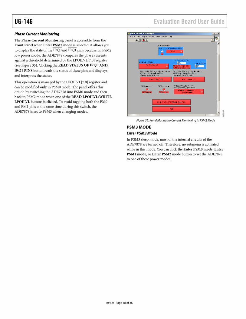
Phase Current Monitoring
The Phase Current Monitoring panel is accessible from the Front Panel when Enter PSM2 mode is selected; it allows you to display the state of the IRQ0and IRQ1 pins because, in PSM2 low power mode, the ADE7878 compares the phase currents against a threshold determined by the LPOILVL[7:0] register (see Figure 35). Clicking the READ STATUS OF IRQ0 AND IRQ1 PINS button reads the status of these pins and displays and interprets the status.
This operation is managed by the LPOILVL[7:0] register and can be modified only in PSM0 mode. The panel offers this option by switching the ADE7878 into PSM0 mode and then back to PSM2 mode when one of the READ LPOILVL/WRITE LPOILVL buttons is clicked. To avoid toggling both the PM0 and PM1 pins at the same time during this switch, the ADE7878 is set to PSM3 when changing modes.
0907
8-03
5
Figure 35. Panel Managing Current Monitoring in PSM2 Mode
PSM3 MODE Enter PSM3 Mode
In PSM3 sleep mode, most of the internal circuits of the ADE7878 are turned off. Therefore, no submenu is activated while in this mode. You can click the Enter PSM0 mode, Enter PSM1 mode, or Enter PSM2 mode button to set the ADE7878 to one of these power modes.

Evaluation Board User Guide UG-146
Rev. 0 | Page 19 of 36
MANAGING THE COMMUNICATION PROTOCOL BETWEEN THE MICROCONTROLLER AND THE ADE7878 In this section, the protocol commands are listed that have been implemented to manage the ADE7878 from the PC using the microcontroller.
The microcontroller is a pure slave during the communication process. It receives a command from the PC, executes the command, and sends an answer to the PC. The PC should wait for the answer before sending a new command to the micro-controller.
Table 3. Echo Command—Message from the PC to the Micro-controller Byte Description 0 A = 0x41 1 N = number of bytes transmitted after this byte 2 Data Byte N − 1 (MSB) 3 Data Byte N − 2 4 Data Byte N − 3 … … N Data Byte 1 N + 1 Data Byte 0 (LSB)
Table 4. Echo Command—Answer from the Microcontroller to the PC Byte Description 0 R = 0x52 1 A = 0x41 2 N = number of bytes transmitted after this byte 3 Data byte N − 1 (MSB) 4 Data byte N − 2 … … N + 1 Data Byte 1 N + 2 Data Byte 0 (LB)
Table 5. Power Mode Select—Message from the PC to the Microcontroller Byte Description 0 B = 0x42, change PSM mode 1 N = 1 2 Data Byte 0: 0x00 = PSM0 0x01 = PSM1 0x02 = PSM2 0x03 = PSM3
Table 6. Power Mode Select—Answer from the Microcon-troller to the PC Byte Description 0 R = 0x52 1 ~ = 0x7E, to acknowledge that the operation was
successful
Table 7. Reset—Message from the PC to the Microcontroller Byte Description 0 C = 0x43, toggle the RESET pin and keep it low for at
least 10 ms 1 N = 1 2 Data Byte 0: this byte can have any value
Table 8. Reset—Answer from the Microcontroller to the PC Byte Description 0 R = 0x52 1 ~ = 0x7E, to acknowledge that the operation was
successful
Table 9. I2C/SPI Select (Configure Communication)—Message from the PC to the Microcontroller Byte Description 0 D = 0x44, select I2C and SPI and initialize them; then set
CONFIG2[7:0] = 0x2 to lock in the port choice. When I2C is selected, also enable SSP0 of the LPC2368 (used for HSDC).
1 N = 1. 2 Data Byte 0: 0x00 = I2C, 0x01 = SPI.
Table 10. I2C/SPI Select (Configure Communication)—Answer from the Microcontroller to the PC Byte Description 0 R = 0x52 1 ~ = 0x7E, to acknowledge that the operation was
successful
Table 11. Data Write—Message from the PC to the Micro-controller Byte Description 0 E = 0x45. 1 N = number of bytes transmitted after this byte. N can
be 1 + 2, 2 + 2, 4 + 2, or 6 + 2. 2 MSB of the address. 3 LSB of the address. 4 Data Byte N − 3 (MSN). 5 Data Byte N − 4. 6 Data Byte N − 5. … … N + 2 Data Byte 1. N + 3 Data Byte 0 (LSB).
Table 12. Data Write—Answer from the Microcontroller to the PC Byte Description 0 R = 0x52 1 ~ = 0x7E, to acknowledge that the operation was
successful

UG-146 Evaluation Board User Guide
Rev. 0 | Page 20 of 36
Table 13. Data Read—Message from the PC to the Micro-controller Byte Description 0 F = 0x46. 1 N = number of bytes transmitted after this byte; N = 3. 2 MSB of the address. 3 LSB of the address. 4 M = number of bytes to be read from the address above.
M can be 1, 2, 4, or 6.
Table 14. Data Read—Answer from the Microcontroller to the PC Byte Description 0 R = 0x52. 1 MSB of the address. 2 LSB of the address. 3 Byte 5, Byte 3, Byte 1, or Byte 0 (MSB) read at the location
indicated by the address. The location may contain 6, 4, 2, or 1 byte. The content is transmitted MSB first.
4 Byte 4, Byte 2, or Byte 0. 5 Byte 3, Byte 1. 6 Byte 2, Byte 0. 7 Byte 1. 8 Byte 0.
Table 15. Interrupt Setup—Message from the PC to the Microcontroller Byte Description 0 J = 0x4A. 1 N = 8, number of bytes transmitted after this byte. 2 MSB of the MASK1[31:0] or MASK0[31:0] register. 3 LSB of the MASK1[31:0] or MASK0[31:0] register. 4 Byte 3 of the desired value of the MASK0[31:0] or
MASK1[31:0] register. 5 Byte 2. 6 Byte 1. 7 Byte 0. 8 Time out byte: time the MCU must wait for the interrupt
to be triggered. It is measured in 3 sec increments. Time out byte (TOB) = 0 means that timeout is disabled.
9 IRQ timer: time the MCU leaves the IRQx pin low before writing back to clear the interrupt flag. It is measured in 10 ms increments. Timer = 0 means that timeout is disabled.
Table 16. Interrupt Setup—Message from the Microcon-troller to the PC Byte Description 0 R = 0x52. 1 Byte 3 of the STATUS0[31:0] or STATUS1[31:0] register.
If the program waited for TOB × 3 sec and the interrupt was not triggered, then Byte 3 = Byte 2 = Byte 1 = Byte 0 = 0xFF.
2 Byte 2 of the STATUS0[31:0] or STATUS1[31:0] register. 3 Byte 1 of the STATUS0[31:0] or STATUS1[31:0] register. 4 Byte 0 of the STATUS0[31:0] or STATUS1[31:0] register.
The microcontroller executes the following operations once the interrupt setup command is received:
1. Reads the STATUS0[31:0] or STATUS1[31:0] register (depending on the address received from the PC) and, if it shows an interrupt already triggered (one of its bits is equal to 1), it erases the interrupt by writing it back.
2. Writes to the MASK0[31:0] or MASK1[31:0] register with the value received from the PC.
3. Waits for the interrupt to be triggered. If the wait is more than the timeout specified in the command, 0xFFFFFFFF is sent back.
4. If the interrupt is triggered, the STATUS0[31:0] or STATUS1[31:0] register is read and then written back to clear it. The value read at this point is the value sent back to the PC so that you can see the source of the interrupts.
5. Sends back the answer.
Table 17. Interrupt Pins Status—Message from the PC to the Microcontroller Byte Description 0 H = 0x48. 1 N = 1, number of bytes transmitted after this byte. 2 Any byte. This value is not used by the program but it is
used in the communication because N must not be equal to 0.
Table 18. Interrupt Pins Status—Answer from the Micro-controller to the PC Byte Description 0 R = 0x52. 1 A number representing the status of the IRQ0 and IRQ1
pins. 0: IRQ0 = low, IRQ1 = low 1: IRQ0 = low, IRQ1 = high. 2: IRQ0 = high, IRQ1 = low. 3: IRQ0 = high, IRQ1 = high. The reason for the IRQ0 and IRQ1 order is that on the microcontroller IO port, IRQ0= P0.1 and IRQ1 = P0.0.

Evaluation Board User Guide UG-146
Rev. 0 | Page 21 of 36
ACQUIRING HSDC DATA CONTINUOUSLY This function acquires data from the HSDC continuously for a defined time period and for up to two variables. The microcon-troller sends data in packages of 4 kB.
Table 19 describes the protocol when two instantaneous phase currents or voltages are acquired.
Table 19. Acquire HSDC Data Continuously—Message from the PC to the Microcontroller If Phase Currents and Voltages Are Acquired Byte Description 0 G = 0x47. 1 N = number of bytes transmitted after this byte. N = 32. 2 0: corresponds to Byte 3 of IA. Because this byte is only a
sign extension of Byte 2, it is not sent back by the microcontroller.
3 Increment_IA_Byte2. If IA is to be acquired, Byte 3, Byte 4, and Byte 5 are 1. Otherwise, they are 0.
4 Increment_IA_Byte1. 5 Increment_IA_Byte2. 6 0. 7 Increment_VA_Byte2. If VA is to be acquired, Byte 7,
Byte 8, and Byte 9 are 1. Otherwise, they are 0. 8 Increment_VA_Byte1. 9 Increment_VA_Byte0. 10 0. 11 Increment_IB_Byte2. If IB is to be acquired, Byte 11,
Byte 12, and Byte 13 are 1. Otherwise, they are 0. 12 Increment_IB_Byte1. 13 Increment_IB_Byte0. 14 0. 15 Increment_VB_Byte2. If VB is to be acquired, Byte 15,
Byte 16, and Byte 17 are 1. Otherwise, they are 0. 16 Increment_VB_Byte1. 17 Increment_VB_Byte0. 18 0. 19 Increment_IC_Byte2. If IC is to be acquired, Byte 19,
Byte 20, and Byte 21 are 1. Otherwise, they are 0. 20 Increment_IC_Byte1. 21 Increment_IC_Byte0. 22 0. 23 Increment_VC_Byte2. If VC is to be acquired, Byte 23,
Byte 24, and Byte 25 are 1. Otherwise, they are 0. 24 Increment_VC_Byte1. 25 Increment_VC_Byte0. 26 0. 27 Increment_IN_Byte2. If IN is to be acquired, Byte 27,
Byte 28, and Byte 29 are 1. Otherwise, they are 0. 28 Increment_IN_Byte1. 29 Increment_IN_Byte0. 30 Byte 1 of M. M is a 16-bit number. The number of 32-bit
samples acquired by the microcontroller is (2 × M + 1) × 67 per channel.
31 Byte 0 of M.
If two of the phase powers are to be acquired, the protocol changes (see Table 20).
Table 20. Acquire HSDC Data Continuously—Message from the PC to the Microcontroller If Phase Powers Are Acquired Byte Description 0 G = 0x47 1 N = number of bytes transmitted after this byte. N = 38. 2 0: corresponds to Byte 3 of AVA. Because this byte is only
a sign extension of Byte 2, it is not sent back by the microcontroller.
3 Increment_AVA_Byte2. If AVA is to be acquired, Byte 3, Byte 4, and Byte 5 are 1. Otherwise, they are 0.
4 Increment_AVA_Byte1. 5 Increment_AVA_Byte2. 6 0. 7 Increment_BVA_Byte2. If BVA is to be acquired, Byte 7,
Byte 8, and Byte 9 are 1. Otherwise, they are 0. 8 Increment_BVA_Byte1. 9 Increment_BVA_Byte0. 10 0. 11 Increment_CVA_Byte2. If CVA is to be acquired, Byte 11,
Byte 12, and Byte 13 are 1. Otherwise, they are 0. 12 Increment_CVA_Byte1. 13 Increment_CVA_Byte0. 14 0. 15 Increment_AWATT_Byte2. If AWATT is to be acquired,
Byte 15, Byte 16, and Byte 17 are 1. Otherwise, they are 0. 16 Increment_AWATT_Byte1. 17 Increment_AWATT_Byte0. 18 0. 19 Increment_BWATT_Byte2. If BWATT is to be acquired,
then Byte 19, Byte 20, and Byte 21 are 1. Otherwise, they are 0.
20 Increment_BWATT_Byte1. 21 Increment_BWATT_Byte0. 22 0. 23 Increment_CWATT_Byte2. If CWATT is to be acquired,
Byte 23, Byte 24, and Byte 25 are 1. Otherwise, they are 0. 24 Increment_CWATT_Byte1. 25 Increment_CWATT_Byte0. 26 0. 27 Increment_AVAR_Byte2. If AVAR is to be acquired,
Byte 27, Byte 28, and Byte 29 are 1. Otherwise, they are 0. 28 Increment_AVAR_Byte1. 29 Increment_AVAR_Byte0. 30 0. 31 Increment_BVAR_Byte2. If BVAR is to be acquired, then
Byte 31, Byte 32, and Byte 33 are 1. Otherwise, they are 0. 32 Increment_BVAR_Byte1. 33 Increment_BVAR_Byte0. 34 0. 35 Increment_CVAR_Byte2. If CVAR is to be acquired,
Byte 35, Byte 36, and Byte 37 are 1. Otherwise, they are 0.

UG-146 Evaluation Board User Guide
Rev. 0 | Page 22 of 36
Byte Description 36 Increment_CVAR_Byte1. 37 Increment_CVAR_Byte0. 38 Byte 1 of M. M is a 16-bit number. The number of 32-bit
samples acquired by the microcontroller is (2 × M + 1) × 67 per channel.
39 Byte 0 of M.
After receiving the command, the microcontroller enables the HSDC port and acquires 67 × 7 × 4 = 1876 bytes into BUFFER0. As soon as BUFFER0 is filled, data is acquired in BUFFER1 (equal in size to BUFFER0), while 2 × 3 × 67 = 402 bytes (134 24-bit words) from BUFFER0 are transmitted to the PC. As soon as BUFFER1 is filled, data is acquired into BUFFER0 while 402 bytes from BUFFER1 are transmitted to the PC. Only the less significant 24 bits of every 32-bit instantaneous value are sent to the PC to decrease the size of the buffer sent to the PC. The most significant eight bits are only an extension of a 24-bit signed word; therefore, no information is lost. The protocol used by the microcontroller to send data to the PC is shown in Table 21.
Table 21. Acquire HSDC Data Continuously—Answer from the Microcontroller to the PC Byte Description 0 R = 0x52 1 Byte 2 (MSB) of Word 1 2 Byte 1 of Word 1 3 Byte 0 (LSB) of Word 1 4 Byte 2 (MSB) of Word 2 5 Byte 1 (MSB) of Word 2 … … 402 Byte 0 (LSB) of Word 134
STARTING THE ADE7878 DSP This function orders the microcontroller to start the DSP. The microcontroller writes to the run register with 0x1.
Table 22. Start ADE7878 DSP—Message from the PC to the Microcontroller Byte Description 0 N = 0x4E 1 N = number of bytes transmitted after this byte; N = 1 2 Any byte
Table 23. Start ADE7878 DSP—Answer from the Micro-controller to the PC Byte Description 0 R = 0x52 1 ~ = 0x7E, to acknowledge that the operation was
successful
STOPPING THE ADE7878 DSP This function orders the microcontroller to stop the DSP. The microcontroller writes to the run register with 0x0.
Table 24. Stop ADE7878 DSP—Message from the PC to the Microcontroller Byte Description 0 O = 0x4F 1 N = number of bytes transmitted after this byte; N = 1 2 Any byte
Table 25. Stop ADE7878 DSP—Answer from the Micro-controller to the PC Byte Description 0 R = 0x52 1 ~ = 0x7E to acknowledge that the operation was
successful

Evaluation Board User Guide UG-146
Rev. 0 | Page 23 of 36
UPGRADING MICROCONTROLLER FIRMWARE Although the evaluation board is supplied with the microcontroller firmware already installed, the ADE7878 evaluation software CD provides the NXP LPC2368 microcontroller project developed under the IAR embedded workbench environment for ARM. Users in possession of this tool can modify the project at will and can download it using an IAR J-link debugger. As an alternative, the executable can be downloaded using a program called Flash Magic, available on the evaluation software CD or at the following website: http://www.flashmagictool.com/.
Flash Magic uses the PC COM port to download the micro-controller firmware. The procedure for using Flash Magic is as follows:
1. Plug a serial cable into connector P15 of the ADE7878 evaluation board and into a PC COM port. As an alternative, use the ADE8052Z-DWDL1 ADE downloader from Analog Devices, Inc., together with a USB cable.
2. Launch the Device Manager under Windows XP by writing devmgmt.msc into the Start/Run box. This helps to identify which COM port is used by the serial cable.
3. Plug the USB2UART board into the P15 connector of the ADE7878 evaluation board with the VDD pin of the USB2UART aligned at Pin 1 of P15.
4. Connect Jumper JP8. The P2.10/EINT0 pin of the microcontroller is now connected to ground.
5. Supply the board with two 3.3 V supplies at the P10 and P12 connectors.
6. Press and release the reset button, S2, on the ADE7878 evaluation board.
7. Launch Flash Magic and do the following: a. Select a COM port (COMx as seen in the Device
Manager). b. Set the baud rate to 115,200. c. Select the NXP LPC2368 device. d. Set the interface to none (ISP). e. Set the DOscillator frequency (MHz) to 12.0. f. Select Erase all Flash + Code Rd Block. g. Choose ADE7878_Eval_Board.hex from the
\Debug\Exe project folder. h. Select Verify after programming.
The Flash Magic settings are shown in Figure 36.
0907
8-03
6
Figure 36. Flash Magic Settings
8. Click Start to begin the download process. 9. After the process finishes, extract the JP8 jumper. 10. Reset the ADE7878 evaluation board by pressing and
releasing the S2 reset button.
At this point, the program should be functional, and a USB cable can be connected to the board. When the PC recognizes the evaluation board and asks for a driver, point it to the project \VirCOM_Driver_XP folder. The ADE7878_eval_board_ vircomport.inf file is the driver.
CONTROL REGISTERS DATA FILE Table 26 shows the order in which the control registers of the ADE7878 are stored into a data file when you click the Save All Regs into a file button in the All Registers Access panel.

UG-146 Evaluation Board User Guide
Rev. 0 | Page 24 of 36
Table 26. Control Register Data File Content Line Number Register 1 AIGAIN 2 AVGAIN 3 BIGAIN 4 BVGAIN 5 CIGAIN 6 CVGAIN 7 NIGAIN 8 AIRMSOS 9 AVRMSOS 10 BIRMSOS 11 BVRMSOS 12 CIRMSOS 13 CVRMSOS 14 NIRMSOS 15 AVAGAIN 16 BVAGAIN 17 CVAGAIN 18 AWGAIN 19 AWATTOS 20 BWGAIN 21 BWATTOS 22 CWGAIN 23 CWATTOS 24 AVARGAIN 25 AVAROS 26 BVARGAIN 27 BVAROS 28 CVARGAIN 29 CVAROS 30 AFWGAIN 31 AFWATTOS 32 BFWGAIN 33 BFWATTOS 34 CFWGAIN 35 CFWATTOS 36 AFVARGAIN 37 AFVAROS 38 BFVARGAIN 39 BFVAROS 40 CFVARGAIN 41 CFVAROS
Line Number Register 42 VATHR1 43 VATHR0 44 WTHR1 45 WTHR0 46 VARTHR1 47 VARTHR0 48 VANOLOAD 49 APNOLOAD 50 VARNOLOAD 51 VLEVEL 52 DICOEFF 53 HPFDIS 54 ISUMLVL 55 RUN 56 OILVL 57 OVLVL 58 SAGLVL 59 MASK0 60 MASK1 61 VNOM 62 LINECYC 63 ZXTOUT 64 COMPMODE 65 Gain 66 CFMODE 67 CF1DEN 68 CF2DEN 69 CF3DEN 70 APHCAL 71 BPHCAL 72 CPHCAL 73 CONFIG 74 MMODE 75 ACCMODE 76 LCYCMODE 77 PEAKCYC 78 SAGCYC 79 CFCYC 80 HSDC_CFG 81 LPOILVL 82 CONFIG2

Evaluation Board User Guide UG-146
Rev. 0 | Page 25 of 36
EVALUATION BOARD SCHEMATICS AND LAYOUT SCHEMATIC
09078-037
NOTE:
MOUNT JP? DIRECTLY BELOW
PAD METAL. CONNECT TO PAD
WITH MULTIPLE VIAS.
REPEAT VIA GRID TO AGND PLANE
EXTRA GROUND TP FOR PROBING
OUTPUT LED CIRCUIT
IRQ1B
CF1
CF2
IRQ0B
CF3
DEVICE INTERFACE HEADER
REFERENCE DECOUPLING AND EXTERNAL REF
RESONANT CIRCUIT. THIS OPTION SHOULD BE PLACED AS
XTAL CKT
BY DEFAULT SELECT OPTION A TO COMPLETE PARALLEL
CLOSE TO DEVICE AS POSSIBLE.
C27
C26
C25
C6
C4
NP
C41
NP
C5
NP
C3
2 1C38
C43
C42
C40
C7
C2
NP
C8
NP
C1
NP
C44
A C
CR5
A C
CR4
A C
CR3
A C
CR2
A C
CR1
RSB
R43
R42
R41
R40
R39
21
E8N
R69
R84
R85
R70
R68
2 31JP12
R35
R36
1TP29
3 421
S1
21
JP3
21
JP4
21
JP5
21
JP6
21JP10
1TP49
2
3
1
A1
1TP51
1TP50
1TP34
1TP36
1TP38
1TP37
1TP39
1TP35
1TP33
1TP32
1TP31
1TP30
1TP28 1
TP27
1TP26 1
TP25
1TP24
1TP23
1TP22
21
JP2
21P
10
R37
1
TP15
1TP14
1TP13
987654 32
31
303 29
28
27
26
25
24
23
22
21
202 19
18
17
16
15
14
13
12
11
101
P11
18
26
19
22
23
39
364
17
32
PAD
38
37
32
29
15
16
13
149
127 8
5 6
28
27
35
34
33
24 25
U1
2
1
3Q5
2
1
3Q2
2
1
3Q4
2
1
3Q3
2
1
3
Q1
21
JP1
21
P9
R38
1TP9
21P5
21
JP7N
R25
21JP8N
54
32
1CLKIN
2 1
Y1
2 31
JP11
DGND_D
CLKOUT
IRQ0B
20PF
20PF
3PIN_SOLDER_JUMPER
BLK
CLKIN
AMP227699-2
BLK
1.0UF
IBP
10K
CF2
CMD28-21VGCTR8T1
BLK
VDD_F
BLK
VDD_F
10UF
VDD
0.1UF
0.1UF
0.1UF
BLK
BLK
BLK
VDD2
VDD
0
BLK
JPR0402
1500 OHMS
VN
BERG69157-102
1K
BERG69157-102
BLK
BLK
REF
EXT_CLKIN
BLK
BLK
BLK
BLK
CF1
SSB/HSA
MOSI/SDA
CF3/HSCLK
IRQ0B
16.384MHZ
IRQ1B
PM0
PM1
RESETB
CLKOUT
EXT_CLKIN SAMTSW-1-30-08-GD
SCLK/SCL
CF2
MISO/HSD
FDV302P
10K
CF3/HSCLK
FDV302P
FDV302P
10K
VDD2
CF1
JPR0402
JPR0402
BLK
WEILAND25.161.0253
VDD2
DVDD
AVDD
3PIN_SOLDER_JUMPER
BLK
BLK
B3S1000
BLK
BLK
BLK
BLK
PAD_CN
VDD_F
ICN
PM0
PM1
VCP
VBP
VAP
CLKIN
INP
INN
VN
CF2
IRQ0B
BERG69157-102
BLK
JPR0402
ADR280ARTZ
10K
499
499
499
ICP
IAN
IAP
RESETB
FDV302P
499
499
2
VDD2
FDV302P
IRQ1B10KCMD28-21VGCTR8T1
CMD28-21VGCTR8T1
CMD28-21VGCTR8T1
CMD28-21VGCTR8T1
XREF
10UF
VDD_F
10UF
VDD_F
10K
JPR0402
4.7UF
MOSI/SDA
IBN
ADE7858CPZ
SCLK/SCL
PAD_CN
BLK
SSB/HSA
MISO/HSD
0.1UF
4.7UF
CF3/HSCLK
CF1
IRQ1B
DVDD
CLKOUT
REF
AVDD
BERG69157-102
BLK
0.22UF
0.22UF
10K
VDD2
0.1UF
VDD
BLK4.7UF
DGND_D
WEILAND25.161.0253
10K
WEILAND25.161.0253
VN_IN
22NF
AGND
DGND
BCOMA
DGND
DGND
AGND
AGND
AGND
DGND
AGND
AGND
AGND
V-
V+
VO
DGND
SCLK_SCL
SS_N_HSA
MISO_HSD
MOSI_SDA
IRQ1_N_SBSDA
IRQ0_N_SBSCL
RESET_N
CF3_HSCLK
CF2
VN
INN
INP
CF1
CLKOUT
CLKIN
VDD
VAP
VBP
VCP
REFIN_OUT
DVDD
PM1
PM0
PADAVDD AGND
DGND
ICN
ICP
IBN
IBP
IAN
IAP
DGND
G
DS
DGND
G
DS
DGND
G
DS
DGND
G
DS
DGND
G
DS
DGND
AGND
AGND
AGND
AGND
AGNDAGND
BCOM
A
Figure 37.

UG-146 Evaluation Board User Guide
Rev. 0 | Page 26 of 36
INPUT ANTI-ALIAS AND DEVICE CONNECTION
C12C11
C20C19
C24C23
C16C15
C22
C14C13
C18C17
C10C9
C21
21E2N
21E1N
21E2C
21E1C
21E1A
21E2A
21E1B
21E2B
2 1JP2N
2 1JP1N
2 1JP2C
2 1JP1C
2 1JP2B
2 1JP1B
2 1JP1A 2 1JP2A
21JP6N
21JP4N
21JP5N
21JP3N
21JP6C
21JP5C
21JP4C
21JP3C
21JP6B
21JP4B
21JP5B
21JP3B
21JP6A
21JP4A
21JP5A
21JP3A
21P421P3
21P1 21P2
1TP7
R7
1TP8
R23
R24
R15
R16
R8
1TP5
R5
1TP6
R21
R22
R13
R14
R6
R4R3
R12
R11
R20
R19
1TP4
1TP3
1TP2
1TP1
R17
R18
R2R1
R10
R9
TBD1206
1500 OHMS
BERG69157-102
100
TBD1206
INN_IN
WEILAND25.161.0253
TBD1206
BERG69157-102 BERG69157-102BERG69157-102
WEILAND25.161.0253
IBP_IN
IBN_IN
BERG69157-102
BERG69157-102
100
TBD1206
100
1K
1K
BERG69157-102
BLK
BERG69157-102BERG69157-102
BERG69157-102
100
1K
BLK
BERG69157-102
IBNIAP
BERG69157-102
BLK
1K
BLK
100
TBD1206
1K
BLK
BERG69157-102
BERG69157-102
TBD1206
100
INP
INN
1500 OHMS
1500 OHMS
TBD1206
1500 OHMS
IAP_IN
ICP
100
BERG69157-102
IBP
BERG69157-102
TBD1206
BERG69157-102
ICN
100
BERG69157-102
BLK
1K
BERG69157-102
1500 OHMS
IAN_IN
1500 OHMS
ICP_IN
BLK
1K
BERG69157-102
1500 OHMS
ICN_IN
WEILAND25.161.0253
BERG69157-102
BERG69157-102
WEILAND25.161.0253
1500 OHMS
1K
BLK
IAN
22NF 22NF
22NF 22NF
22NF
22NF
22NF
22NF
BERG69157-102
BERG69157-102
INP_IN
22NF 22NF
22NF 22NF
22NF 22NF
22NF 22NF
AGND
AGND
AGND
AGND
AGND
AGND
AGND
AGND
AGND
AGND
AGND
AGND
09078-043
Figure 38.

Evaluation Board User Guide UG-146
Rev. 0 | Page 27 of 36
PHASE A VOLTAGE
PHASE C VOLTAGE
PHASE B VOLTAGE
C34
C33
C32
R26
R28
R27
21
E8C
21
E8B
21
E8A
1TP10
2 31
JP9C
21
P6
21
JP8C
R31
2 1JP7C
R34
21
P7
21
JP8B
R30
2 1JP7B
R33
1TP11
2 31
JP9B
21
JP8A
1TP12
2 1JP7A
21
P8
2 31
JP9A
R32
R29
22NF
3PIN_SOLDER_JUMPER
BERG69157-102
1K1500 OHMS
WEILAND25.161.0253
WEILAND25.161.0253
BERG69157-102
1K
BLK
3PIN_SOLDER_JUMPER
VBP
1500 OHMS
VCP_IN
VBP_IN
VN
100K
BERG69157-102
1500 OHMS
1K
BERG69157-102
VN
BLK
100K
BERG69157-102
1M
1M
WEILAND25.161.0253
1M
3PIN_SOLDER_JUMPER
100K
BERG69157-102
VCP
VN
BLKVAP
VAP_IN
22NF
22NF
B
COMA
AGND
AGNDAGND
AGND
AGNDAGND
B
COMA
AGND
AGND
AGND
B
COMA
0907
8-04
4
Figure 39.

UG-146 Evaluation Board User Guide
Rev. 0 | Page 28 of 36
BYPASSING CONTROLLER
(OPTIONAL; CUSTOMER SUPPLIED)
TP FOR EVAL PROBE - DISTRIBUTE AROUND ISOLATED CIRCUITS
NC
D-
D+
GND
VBUS(5V)
USB IF
MRESET
MCU CIRCUIT
UART
SHIELD D+, D-, VREF_MCU WITH GND
FROM CONN TO MCU
ISOLATED PSU CONNECTIONS
P2_11
P2_12
PM0_CTRL
P1_29
P1_28
P1_27
P1_19
CF3_HSCLK_ISO
P2_9
P2_8
P2_7
P2_6
PM1_CTRL
MCU_XT2
P1_15
SSB_ISO
CF2_ISO
P4_29
IRQ1B_ISO
P1_26
P1_25
P1_0
P1_4
P1_8
MCU_XT1
TMS
P1_22
P0_24
P0_26
MOSI_ISO
GND
GND
GND
AMP227699-2
CF1_ISO
CF2_ISO
AMP227699-2
AMP227699-2
CF3_HSCLK_ISO
P0_20
SML-LXT0805GW-TR
BLK
680
CF3_HSCLK_ISO
IRQ0B_ISO
P2_13
10K
RTCK
0.1UF
WEILAND25.161.0253
MCU_VDD_ISO
10K
BERG69157-102
P2_2
SAMTSW-1-30-08-GD
RXD
TXD
10K
BLK
P1_31
MCU_RST
SAMTECTSW10608GS4PIN
MCU_VDD
10K
27
BLK
MCU_VDD
10UF
0.1UF
1UF
0.1UF
0.1UF
0.1UF
0.1UF
0.1UF
0.1UF
0.1UF
0.1UF
0.1UF
1.5K
P1_23
MCU_VDD
MCU_VDD
10K
LPC2368FBD100
P0_22
MCU_VDD
D+
D-
D-_MCU
D+_MCU
VBUS
27
4-1734376-8
RSTOUT_N
RTCX2
P1_1
USB_UP
P4_28
P3_26
P3_25
D+_MCU
SDA_ISO
IRQ_OUT_EN_ISO
IRQ_IN_EN
MISO_ISO
SCLK_ISO
RESB_CTRL
PM0_CTRL
IRQ1B_ISO
PM1_CTRL
SBENB_ISO
SSB_ISO
TCLK
TRST_N
TDI
10K
10K P0_21
P0_19
P0_5
D-_MCU
RXD
TXD
WP
P0_4
P0_9
BLK
BLK
BLK
BLK
BLK
BLK
BLK
BLK
BLK
BLK
VBUS
P2_1
P2_0
P2_3
P2_5
HSDATA_ISO
MCU_XT1
20PF
MCU_XT2
20PF
12.000MHZ
MCU_RST
MCU_VDD
B3S1000
10K
P1_9
P1_17
P1_14
P1_10
P1_16
MCU_VDD
SAMTECTSW11008GD
TMS
10K
10K
TDI
TCLK
RTCK
TDO
MCU_RST
10K
TDO
SCL_ISO
TRST_N
HSA_ISO
BLK
BLK
BLK
P2_4
IRQ0B_ISO
MCU_RST
RESB_CTRL
HSA_ISO
MOSI_ISO
SDA_ISO
MISO_HSD_ISO
SCLK_ISO
SCL_ISO
CF1_ISO
R79
R80
R81
TP46
1
TP42
1
TP43
1
TP41
1
P15
1 2 3 4
R82
P12
1 2
C78P N
C79
TP16
1TP17
1TP18
1
CF3
1
2345
CF2
1
2345
CF1
1
2345
C72
U8
46
48
49
62
63
61
60
59
47
58
57
56 98 76
25
24
29
98
30
99818079
78
77
76
95
90898887863233
94
343536373839404344452120
939291
75
535251
50
747370696867666564
27268285
17
14
10016
18
521
3 4
19
285471
96
134284
10
12
15314155728397
11
22
23
C75
C73
C76
C77
C83
C84
C80
C81
C82
R78
P13
1 101112131415161718192 203 4 5 6 7 8 9
R44
R45
R75
R73
R72 R71
R83
TP52
1
TP44
1
TP54
1
TP45
1
TP55
1
TP53
1
TP48
1
TP47
1
TP40
1
S2
1 243
R74
C74
Y2
12
C70
C71
CR6
CA
R77
P14
12 3
4 56
R76
JP7
12
P38
1 101112131415161718192 202122232425262728293 3031324 5 6 7 8 9
P2_10
TRST_N
TCK
P1_18_USB_UP_LED_PWM1_1
VBAT
VREF
VDDA
VDD_DCDC_3V3_3
VDD_DCDC_3V3_2
VDD_DCDC_3V3_1
VDD_3V3_4
VDD_3V3_3
VDD_3V3_2
VDD_3V3_1
VSSA
VSS
P1_0_ENET_TXD0
P2_12_EINT2_MCIDAT2_I2STX_WS
P2_11_EINT1_MCIDAT1_I2STX_CLK
P2_10_EINT0
P2_9_USB_CONNECT_RXD2_EXTIN0
P2_8_TD2_TXD2_TRACEPKT3
P2_7_RD2_RTS1_TRACEPKT2
P2_6_PCAP1_0_RI1_TRACEPKT1
P2_5_PWM1_6_DTR1_TRACEPKT0
P2_4_PWM1_5_DSR1_TRACESYNC
P2_3_PWM1_4_DCD1_PIPESTAT2
P2_2_PWM1_3_CTS1_PIPESTAT1
P2_1_PWM1_2_RXD1_PIPESTAT0
P2_0_PWM1_1_TXD1_TRACECLK
P1_31_SCK1_AD0_5
P1_30_VBUS_AD0_4
P1_29_PCAP1_1_MAT0_1
P1_28_PCAP1_0_MAT0_0
P1_27_CAP0_1
P1_26_PWM1_6_CAP0_0
P1_25_MAT1_1
P1_24_PWM1_5_MOSI0
P1_23_PWM1_4_MISO0
P1_22_MAT1_0
P1_21_PWM1_3_SSEL0
P1_20_PWM1_2_SCK0
P1_19_CAP1_1
P1_17_ENET_MDIO
P1_16_ENET_MDC
P1_15_ENET_REF_CLK
P1_14_ENET_RX_ER
P1_10_ENET_RXD1
P1_9_ENET_RXD0
P1_8_ENET_CRS
P1_4_ENET_TX_EN
P1_1_ENET_TXD1
RTCX2
XTAL2
RSTOUT_N
TDO
RTCK
P2_13_EINT3_MCIDAT3_I2STX_SDA
P4_29_MAT2_1_RXD3
P4_28_MAT2_0_TXD3
P3_26_MAT0_1_PWM1_3
P3_25_MAT0_0_PWM1_2
P0_30_USB_DN
P0_29_USB_DP
P0_28_SCL0
P0_27_SDA0
P0_26_AD0_3_AOUT_RXD3
P0_25_AD0_2_I2SRX_SDA_TXD3
P0_24_AD0_1_I2SRX_WS_CAP3_1
P0_23_AD0_0_I2SRX_CLK_CAP3_0
P0_22_RTS1_MCIDAT0_TD1
P0_21_RI1_MCIPWR_RD1
P0_20_DTR1_MCICMD_SCL1
P0_19_DSR1_MCICLK_SDA1
P0_18_DCD1_MOSI0_MOSI
P0_17_CTS1_MISO0_MISO
P0_16_RXD1_SSEL0_SSEL
P0_15_TXD1_SCK0_SCK
P0_11_RXD2_SCL2_MAT3_1
P0_10_TXD2_SDA2_MAT3_0
P0_9_I2STX_SDA_MOSI1_MAT2_3
P0_8_I2STX_WS_MISO1_MAT2_2
P0_7_I2STX_CLK_SCK1_MAT2_1
P0_6_I2SRX_SDA_SSEL1_MAT2_0
P0_5_I2SRX_WS_TD2_CAP2_1
P0_4_I2SRX_CLK_RD2_CAP2_0
P0_3_RXD0
P0_2_TXD0
P0_1_TD1_RXD3_SCL1
P0_0_RD1_TXD3_SDA1
RTCX1
XTAL1
RESET_N
TMS
TDI
09078-038
Figure 40.

Evaluation Board User Guide UG-146
Rev. 0 | Page 29 of 36
<- DUT
ISOLATION CIRCUIT
I2C/HSDC CONFIG SPI CONFIGSPI CONFIGI2C/HSDC CONFIG
MCU ->
0
SDA_ISO
SDA_ISO
0.1UF
0.1UF
0.1UF
0.1UF
0.1UF
0.1UF
0.1UF
0.1UF
0.1UF
0.1UF
SB_ENB
SCL_ISOSCLSDA
SCLK
SSBMOSI
SCLK_ISOMOSI_ISOSSB_ISO
IRQ_OUT_EN
MISO_HSD_ISOCF3_HSCLK_ISOHSA_ISO
VE2_U6MISO/HSDCF3/HSCLKHSACTIVE
IRQ_OUT_EN_ISO
IRQ1BWP_UX
IRQ0BIRQ1BCF2
IRQ_IN_EN
SBENB_ISO
CF1_ISO
RESETBPM0PM1
RESB_CTRL
PM1_CTRLCF1
ADUM1401BRWZ
10K
VE2_U3
10K
ADUM1401BRWZ
HSDATA_ISO
SCLK/SCL
SDA
VDD2MCU_VDD
SCL
IRQ1B_ISO
IRQ1B_ISOIRQ0B_ISO
10K
VE2_U6
10K
ADUM1401BRWZ
10K
HSACTIVE SSB/HSA
SCL
SSB
SCLK
0
0
MISO_ISOMISO_HSD_ISO
0 0
SCL_ISO
10K
10K
ADUM1401BRWZ
10K
10K
10K
ADUM1401BRWZ
IRQ_IN_EN
CF2_ISO
IRQ0B_ISO
10K
10K
PM0_CTRL
VE2_U3
WP
IRQ0B
0.1UF
10K
IRQ_OUT_EN
0.1UF
ADUM1250ARZ
MOSI/SDA
0SDA
DNI
DNI
DNI
DNI
MOSI
0
10K
0
A2
4 5
3 62 7
1 8
U4
2 8 915
1 16
710345
11
1413126
U3
28915
116
71034511
1413126
U6
2 8 915
1 16
710345
11
1413126
R48 R49
R51
R55
R54
JP35
JP33
JP37
JP361 2
JP341 2
JP381 2JP32
1 2JP31
C58
C59
R58B
R58A
R59B
R59A
C56
C57
U7
28915
116
71034511
1413126
R57
R53U5
28915
116
71034511
1413126
R50
R46
R47
C55
C54
C53
C52
C51
C50
C49
C48
GND2
VDD2
VOAVOB
VICVID
VE2
GND1
VE1
VODVOC
VIBVIA
VDD1
GND2
VDD2
VOAVOB
VICVID
VE2
GND1
VE1
VODVOC
VIBVIA
VDD1
GND2
VDD2
VOAVOB
VICVID
VE2
GND1
VE1
VODVOC
VIBVIA
VDD1
DGNDGND
SCL2SCL1SDA2SDA1
VDD1 VDD2
GND1 GND2
GND2
VDD2
VOAVOB
VICVID
VE2
GND1
VE1
VODVOC
VIBVIA
VDD1
GND2
VDD2
VOAVOB
VICVID
VE2
GND1
VE1
VODVOC
VIBVIA
VDD1
0907
8-04
5
Figure 41.

UG-146 Evaluation Board User Guide
Rev. 0 | Page 30 of 36
09078-039
LEFT MOST PINS SHOULD BE FURTHEST FROM DUT 26
ALIGN PORTS AS DRAWN NEXT TO MCU
SIDE WITH PINS76 - 100
100
75
50
25
DO NOT INSTALL
SIDE WITH PINS1 - 25
DO NOT INSTALL
SIDE WITH PINS51 - 75
DO NOT INSTALL
DO NOT INSTALL
ALIGN PORTS AS DRAWN NEXT TO MCU
ALIGN PORTS AS DRAWN NEXT TO MCU
1
SIDE WITH PINS26 - 50
ALIGN PORTS AS DRAWN NEXT TO MCU
51
76
R52
2 1JP9
R56
2 1
JP8
R86
54321P19
54321P21
54321P25
54321P29
54321P33
54321P37
54321P20
54321P24
54321P28
54321P32
54321P36
54321P23
54321P27
54321P35
54321P31
54321P26
54321P30
54321P34
54321P22
54321P18
P1_29
SAMTECTSW10608GS5PIN
BERG69157-102
SAMTECTSW10608GS5PIN
P3_25
D+_MCU
P2_10
SAMTECTSW10608GS5PIN
P0_20
SAMTECTSW10608GS5PIN
DNI
DNI
DNI
DNI
DNI
DNI
DNI
DNI
DNI
DNI
DNI
DNI
DNI
DNI
DNI
DNI
DNI
DNI
DNI
TDO
SAMTECTSW10608GS5PIN
SAMTECTSW10608GS5PIN
MISO_ISO
SAMTECTSW10608GS5PIN
P1_28
P1_22
SAMTECTSW10608GS5PIN
SAMTECTSW10608GS5PIN
SAMTECTSW10608GS5PINHSA_ISO
P1_19
USB_UP
P0_19
P0_21
TDI
SAMTECTSW10608GS5PIN
SAMTECTSW10608GS5PINP0_5
PM1_CTRL
P3_26
P2_12
P0_9
SAMTECTSW10608GS5PINMCU_XT2
SCL_ISO
VBUS
MCU_XT1
SAMTECTSW10608GS5PINP1_31
WP
IRQ0B_ISO
IRQ1B_ISO
P2_13
P2_0
P2_1
P2_2
SAMTECTSW10608GS5PINP1_27
P2_6
P2_4
P2_5
RXD
TXD
RTCK
SAMTECTSW10608GS5PIN
P1_8
P1_0
RSTOUT_N
P1_26
P1_25
P1_23
P2_8
P2_9
SSB_ISO
SCLK_ISO
SAMTECTSW10608GS5PIN
P1_16
P1_17
P1_10
P1_15
P1_14
P1_4
P1_1
P1_9
CF3_HSCLK_ISO
SDA_ISO
MCU_RST
RTCX2
PM0_CTRL
SBENB_ISO
D-_MCU
P4_29
MOSI_ISO
P2_3
TMS
P0_26
IRQ_OUT_EN_ISO
SAMTECTSW10608GS5PIN
SAMTECTSW10608GS5PIN
DNI
TRST_N
TCLK
IRQ_IN_EN
P2_11
P0_22
P0_4
P4_28
RESB_CTRL
10K
BERG69157-102
10K
10K
P0_24
MCU_VDD
P2_7
HSDATA_ISO
P0_24
SAMTECTSW10608GS5PIN
GND
GND
Figure 42.

Evaluation Board User Guide UG-146
Rev. 0 | Page 31 of 36
DO NOT POPULATE U2
SELF BOOT EEPROMFACTORY USE ONLY
CURRENT MEASUREMENT - DO NOT INSTALL
C61
C62
C63
R66
R65
1TP61
1TP62
21
P17
4
8
2
6
3
1
A3
R62
2 1JP60
2 1JP61
R61
R63
R60
7
4
2
95
3
10
1
8
6
A4
321
P16
R64
7
4
8
56
321U2
0.1UF
VDD2
VDD2
10K
MICRO24LC128-I-SN
0.1UF WP_UX
SBSCL
DNI
DNI
BLK
BLK
ISNS_OUT
WEILAND25.161.0253AD8553ARMZ
DNI
DNI560PF
VDD_F
200K
IRQ0B
DNI
DNI4.02K
DNI
DNIDO NOT INSTALL DNI
100K
100K
VREF_ISNS
VDD
DNI
10K
VDD2
SBSCL
VDD2
0
0SBSDA IRQ1B
10K
SBCON
SBCON
SB_ENB
MOLEX22-03-2031
SBSDA
ADG820BRMZ
DNIDGND
DGND
DGND
DGND
VDD
S2
S1
IN
GND
D
VFB
GND
VREF
EN
VCC
VO
RGB
RGA
SCLA1
A2
A0 WP
SDAVSS
VCC
0907
8-04
6
Figure 43.

UG-146 Evaluation Board User Guide
Rev. 0 | Page 32 of 36
LAYOUT
0907
8-04
0
Figure 44.
0907
8-04
1
Figure 45.

Evaluation Board User Guide UG-146
Rev. 0 | Page 33 of 36
0907
8-04
2
Figure 46.
0907
8-04
3
Figure 47.

UG-146 Evaluation Board User Guide
Rev. 0 | Page 34 of 36
ORDERING INFORMATION BILL OF MATERIALS
Table 27. Qty Designator Description Manufacturer/Part Number 1 A1 IC-ADI, 1.2 V, ultralow power, high PSRR voltage
reference Analog Devices, Inc./ADR280ARTZ
1 A2 IC swappable dual isolator Analog Devices, Inc./ADUM1250ARZ
4 C1, C8, C44, C78 Capacitor, tantalum, 10 μF AVX 20 C9 to C25, C32 to C34 Capacitor, ceramic, 22 nF AVX
30 C2, C7, C40, C42, C43, C48 to C59, C61, C62, C72, C73, C75 to C77, C79 to C84
Capacitor, chip, X7R 0805, 0.1 μF Murata
4 C26, C27, C70, C71 Capacitor, mono, ceramic, C0G, 0402, 20 pF Murata
3 C3, C5, C41 Capacitor, tantalum, 4.7 μF AVX 2 C38, C74 Capacitor, ceramic chip, 1206, X7R, 1.0 μF Taiyo Yuden
2 C4, C6 Capacitor, ceramic, X7R, 0.22 μF Phycomp (Yageo) 4 CF1 to CF3, CLKIN Connector, PCB coax, BNC, ST AMP (Tyco)/227699-2
5 CR1 to CR5 Diode, LED, green, SMD Chicago Mini Lamp (CML Innovative Technologies)/CMD28-21VGCTR8T1
1 CR6 LED, green, surface mount LUMEX/SML-LXT0805GW-TR
12 E1A, E1B, E1C, E1N, E2A, E2B, E2C, E2N, E8A, E8B, E8C, E8N
Inductor, chip, ferrite bead, 0805, 1500 Ω Murata
37 JP2, JP7 to JP10, JP1A to JP8A, JP1B to JP8B, JP1C to JP8C, JP1N to JP8N
Connector, PCB Berg jumper, ST, male 2-pin Berg/69157-102
5 JP11, JP12, JP9A, JP9B, JP9C 3-pin solder jumper N/A 6 JP32, JP34, JP36, JP38, JP60, JP61 Resistor jumper, SMD 0805 (open), 0 Ω Panasonic
11 P1 to P10, P12 Connector, PCB TERM, black, 2-pin, ST WeilandD/25.161.0253 2 P11, P38 Connector, PCB, header, SHRD, ST, male 32-pin Samtec/TSW-1-30-08-G-D
1 P13 Connector, PCB, Berg, header, ST, male 20-pin Samtec/TSW-110-08-G-D 1 P14 Connector, PCB, USB, Type B, R/A, through hole AMP (Tyco)/4-1734376-8
1 P15 Connector, PCB, Berg, header, ST, male 4-pin Samtec/TSW106-08-G-S 1 P16 Connector, PCB straight header 3-pin Molex/22-03-2031
5 Q1 to Q5 Trans digital FET P channel Fairchild/FDV302P 8 R1 to R8 Do not install (TBD_R1206) N/A
8 R9 to R16 Resistor, PREC, thick film chip, R1206, 100 Ω Panasonic 12 R17 to R25, R32 to R34 Resistor, PREC, thick film chip, R0805, 1 kΩ Panasonic
3 R26 to R28 Resistor, MF, RN55, 1 M Vishay-Dale 3 R29 to R31 Resistor, MF, RN5, 100 kΩ Vishay-Dale
39 R35, R36, R38, R44 to R57, R64 to R66, R68 to R76, R78, R82 to R86, R58A, R58B, R59A, R59B
Resistor PREC thick film chip, R0805, 10 kΩ Panasonic
1 R37 Resistor, film, SMD 0805, 2 Ω Panasonic
5 R39 to R43 Resistor, PREC, thick film chip, R1206, 499 Panasonic 1 R77 Resistor, film, SMD, 0805, 680 Ω Multicomp
2 R79, R80 Resistor, film, SMD, 1206, 27 Ω Yageo-Phycomp 1 R81 Resistor, PREC, thick film chip, R1206, 1.5 kΩ Panasonic
1 RSB Resistor, jumper, SMD, 1206 (open), 0 Panasonic 2 S1, S2 SW SM mechanical key switch Omron/B3S1000
52 TP1 to TP18, TP22 to TP55 Connector, PCB, test point, black Components Corporation 1 U1 IC-ADI, polyphase, multifunction, energy metering IC Analog Devices, Inc./ADE7878CPZ
5 U3 to U7 IC-ADI quad channel digital isolator Analog Devices, Inc./ADum1401BRWZ 1 U8 IC ARM7, MCU, flash, 512 kΩ, 100 LQFP NXP/LPC2368FBD100

Evaluation Board User Guide UG-146
Rev. 0 | Page 35 of 36
Qty Designator Description Manufacturer/Part Number 1 Y1 IC crystal, 16.384 MHz Valpey Fisher Corporation 1 Y2 IC crystal quartz, 12.000 MHz ECS
1 A3 IC-ADI 1.8 V to 5.5 V 2:1 MUX/SPDT switches Analog Devices, Inc./ADG820BRMZ 1 A4 IC-ADI 1.8 V to 5 V auto-zero in amp with shutdown Analog Devices, Inc./AD8553ARMZ
1 C63 Capacitor, ceramic, NP0, 560 pF Phycomp (Yageo) 4 JP31, JP33, JP35, JP37 Resistor, jumper, SMD, 0805 (SHRT), 0 Panasonic
1 P17 Connector, PCB, TERM, black, 2-pin, ST Weiland/25.161.0253 20 P18 to P37 Connector, PCB, Berg, header, ST, male 5-pin Samtec/TSW106-08-G-S
1 R60 Resistor, PREC, thick film chip, R0805, 4.02 kΩ Panasonic 2 R61, R62 Resistor, PREC, thick film chip, R0805, 100 kΩ Panasonic
1 R63 Resistor, PREC, thick film chip, R1206, 200 kΩ Panasonic 2 TP61, TP62 Connector, PCB test point, black Components Corporation
1 U2 IC, serial EEPROM, 128 kΩ, 2.5 V Microchip/24LC128-I-SN

UG-146 Evaluation Board User Guide
Rev. 0 | Page 36 of 36
NOTES
I2C refers to a communications protocol originally developed by Philips Semiconductors (now NXP Semiconductors).
ESD Caution ESD (electrostatic discharge) sensitive device. Charged devices and circuit boards can discharge without detection. Although this product features patented or proprietary protection circuitry, damage may occur on devices subjected to high energy ESD. Therefore, proper ESD precautions should be taken to avoid performance degradation or loss of functionality.
Legal Terms and Conditions By using the evaluation board discussed herein (together with any tools, components documentation or support materials, the “Evaluation Board”), you are agreeing to be bound by the terms and conditions set forth below (“Agreement”) unless you have purchased the Evaluation Board, in which case the Analog Devices Standard Terms and Conditions of Sale shall govern. Do not use the Evaluation Board until you have read and agreed to the Agreement. Your use of the Evaluation Board shall signify your acceptance of the Agreement. This Agreement is made by and between you (“Customer”) and Analog Devices, Inc. (“ADI”), with its principal place of business at One Technology Way, Norwood, MA 02062, USA. Subject to the terms and conditions of the Agreement, ADI hereby grants to Customer a free, limited, personal, temporary, non-exclusive, non-sublicensable, non-transferable license to use the Evaluation Board FOR EVALUATION PURPOSES ONLY. Customer understands and agrees that the Evaluation Board is provided for the sole and exclusive purpose referenced above, and agrees not to use the Evaluation Board for any other purpose. Furthermore, the license granted is expressly made subject to the following additional limitations: Customer shall not (i) rent, lease, display, sell, transfer, assign, sublicense, or distribute the Evaluation Board; and (ii) permit any Third Party to access the Evaluation Board. As used herein, the term “Third Party” includes any entity other than ADI, Customer, their employees, affiliates and in-house consultants. The Evaluation Board is NOT sold to Customer; all rights not expressly granted herein, including ownership of the Evaluation Board, are reserved by ADI. CONFIDENTIALITY. This Agreement and the Evaluation Board shall all be considered the confidential and proprietary information of ADI. Customer may not disclose or transfer any portion of the Evaluation Board to any other party for any reason. Upon discontinuation of use of the Evaluation Board or termination of this Agreement, Customer agrees to promptly return the Evaluation Board to ADI. ADDITIONAL RESTRICTIONS. Customer may not disassemble, decompile or reverse engineer chips on the Evaluation Board. Customer shall inform ADI of any occurred damages or any modifications or alterations it makes to the Evaluation Board, including but not limited to soldering or any other activity that affects the material content of the Evaluation Board. Modifications to the Evaluation Board must comply with applicable law, including but not limited to the RoHS Directive. TERMINATION. ADI may terminate this Agreement at any time upon giving written notice to Customer. Customer agrees to return to ADI the Evaluation Board at that time. LIMITATION OF LIABILITY. THE EVALUATION BOARD PROVIDED HEREUNDER IS PROVIDED “AS IS” AND ADI MAKES NO WARRANTIES OR REPRESENTATIONS OF ANY KIND WITH RESPECT TO IT. ADI SPECIFICALLY DISCLAIMS ANY REPRESENTATIONS, ENDORSEMENTS, GUARANTEES, OR WARRANTIES, EXPRESS OR IMPLIED, RELATED TO THE EVALUATION BOARD INCLUDING, BUT NOT LIMITED TO, THE IMPLIED WARRANTY OF MERCHANTABILITY, TITLE, FITNESS FOR A PARTICULAR PURPOSE OR NONINFRINGEMENT OF INTELLECTUAL PROPERTY RIGHTS. IN NO EVENT WILL ADI AND ITS LICENSORS BE LIABLE FOR ANY INCIDENTAL, SPECIAL, INDIRECT, OR CONSEQUENTIAL DAMAGES RESULTING FROM CUSTOMER’S POSSESSION OR USE OF THE EVALUATION BOARD, INCLUDING BUT NOT LIMITED TO LOST PROFITS, DELAY COSTS, LABOR COSTS OR LOSS OF GOODWILL. ADI’S TOTAL LIABILITY FROM ANY AND ALL CAUSES SHALL BE LIMITED TO THE AMOUNT OF ONE HUNDRED US DOLLARS ($100.00). EXPORT. Customer agrees that it will not directly or indirectly export the Evaluation Board to another country, and that it will comply with all applicable United States federal laws and regulations relating to exports. GOVERNING LAW. This Agreement shall be governed by and construed in accordance with the substantive laws of the Commonwealth of Massachusetts (excluding conflict of law rules). Any legal action regarding this Agreement will be heard in the state or federal courts having jurisdiction in Suffolk County, Massachusetts, and Customer hereby submits to the personal jurisdiction and venue of such courts. The United Nations Convention on Contracts for the International Sale of Goods shall not apply to this Agreement and is expressly disclaimed.
©2010 Analog Devices, Inc. All rights reserved. Trademarks and registered trademarks are the property of their respective owners. UG09078-0-8/10(0)