Embed Size (px)
Citation preview
Poly Phase Multifunction Energy Metering IC with Per Phase Information
Data Sheet ADE7758
Rev. E Information furnished by Analog Devices is believed to be accurate and reliable. However, no responsibility is assumed by Analog Devices for its use, nor for any infringements of patents or other rights of third parties that may result from its use. Specifications subject to change without notice. No license is granted by implication or otherwise under any patent or patent rights of Analog Devices. Trademarks and registered trademarks are the property of their respective owners.
One Technology Way, P.O. Box 9106, Norwood, MA 02062-9106, U.S.A.Tel: 781.329.4700 www.analog.com Fax: 781.461.3113 ©2004–2011 Analog Devices, Inc. All rights reserved.
FEATURES Highly accurate; supports IEC 60687, IEC 61036, IEC 61268,
IEC 62053-21, IEC 62053-22, and IEC 62053-23 Compatible with 3-phase/3-wire, 3-phase/4-wire, and other
3-phase services Less than 0.1% active energy error over a dynamic range of
1000 to 1 at 25°C Supplies active/reactive/apparent energy, voltage rms,
current rms, and sampled waveform data Two pulse outputs, one for active power and the other
selectable between reactive and apparent power with programmable frequency
Digital power, phase, and rms offset calibration On-chip, user-programmable thresholds for line voltage SAG
and overvoltage detections An on-chip, digital integrator enables direct interface-to-
current sensors with di/dt output A PGA in the current channel allows direct interface to
current transformers An SPI®-compatible serial interface with IRQ
Proprietary ADCs and DSP provide high accuracy over large variations in environmental conditions and time
Reference 2.4 V (drift 30 ppm/°C typical) with external overdrive capability
Single 5 V supply, low power (70 mW typical)
GENERAL DESCRIPTION The ADE7758 is a high accuracy, 3-phase electrical energy measurement IC with a serial interface and two pulse outputs. The ADE7758 incorporates second-order Σ-Δ ADCs, a digital integrator, reference circuitry, a temperature sensor, and all the signal processing required to perform active, reactive, and apparent energy measurement and rms calculations.
The ADE7758 is suitable to measure active, reactive, and apparent energy in various 3-phase configurations, such as WYE or DELTA services, with both three and four wires. The ADE7758 provides system calibration features for each phase, that is, rms offset correction, phase calibration, and power calibration. The APCF logic output gives active power information, and the VARCF logic output provides instantaneous reactive or apparent power information.
FUNCTIONAL BLOCK DIAGRAM
PHASE BAND
PHASE CDATA
4
AVDD
POWERSUPPLY
MONITOR
12
REFIN/OUT11
AGND
ADC–
+9ICP
10ICN
PGA1
ADC–
+14VCP
13VN
PGA2ACTIVE/REACTIVE/AP PARENT ENERGIES
AND VOLTAGE/CURRENT RMS CALCUL ATIONFOR PHASE C
(SEE PHASE A FOR DETAILED SIGNAL PATH)
ADC–
+7IBP
8IBN
PGA1
ADC–
+15VBPPGA2
ACTIVE/REACTIVE/AP PARENT ENERGIESAND VOLTAGE/CURRENT RMS CALCUL ATION
FOR PHASE B(SEE PHASE A FOR DETAILED SIGNAL PATH)
ADC–
+5IAP
6IAN
PGA1
ADC–
+16VAPPGA2
AVRMSGAIN[11:0]AVAG[11:0]
|X|
APHCAL[6:0]
Φ
HPF INTEGRATORdt
AVAROS[11:0] AVARG[11:0]LPF2
90° PHASESHIFTING FILTER
π2
AWATTOS[11:0] AWG[11:0]LPF2
22
DIN24
DOUT23
SCLK21
CS18
IRQ
ADE7758 REGISTERS ANDSERIAL INTERFACE
WDIV[7:0] %
VARDIV[7:0] %
VADIV[7:0] %
AIRMSOS[11:0]
X2
LPF2.4VREF
4kΩ
DFC ÷
APCFNUM[11:0]
APCFDEN[11:0]
ACTIVE POWER
1 APCF
3 DVDD2 DGND
19 CLKIN20 CLKOUT
DFC
VARCFNUM[11:0]
VARCFDEN[ 11:0]
REACTIVE ORAPPARENT POWER
17 VARCF
ADE7758
AVRMSOS[11:0]
0444
3-00
1
÷
Figure 1.
ADE7758 Data Sheet
Rev. E | Page 2 of 72
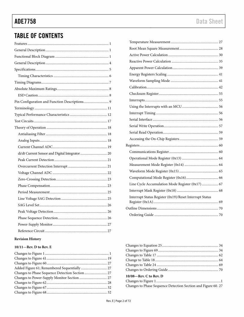
TABLE OF CONTENTS Features .............................................................................................. 1
General Description ......................................................................... 1
Functional Block Diagram .............................................................. 1
General Description ......................................................................... 4
Specifications..................................................................................... 5
Timing Characteristics ................................................................ 6
Timing Diagrams.............................................................................. 7
Absolute Maximum Ratings............................................................ 8
ESD Caution.................................................................................. 8
Pin Configuration and Function Descriptions............................. 9
Terminology .................................................................................... 11
Typical Performance Characteristics ........................................... 12
Test Circuits..................................................................................... 17
Theory of Operation ...................................................................... 18
Antialiasing Filter ....................................................................... 18
Analog Inputs.............................................................................. 18
Current Channel ADC............................................................... 19
di/dt Current Sensor and Digital Integrator............................... 20
Peak Current Detection ............................................................. 21
Overcurrent Detection Interrupt ............................................. 21
Voltage Channel ADC ............................................................... 22
Zero-Crossing Detection........................................................... 23
Phase Compensation.................................................................. 23
Period Measurement .................................................................. 25
Line Voltage SAG Detection ..................................................... 25
SAG Level Set .............................................................................. 26
Peak Voltage Detection.............................................................. 26
Phase Sequence Detection......................................................... 26
Power-Supply Monitor............................................................... 27
Reference Circuit ........................................................................ 27
Temperature Measurement ....................................................... 27
Root Mean Square Measurement............................................. 28
Active Power Calculation.......................................................... 30
Reactive Power Calculation ...................................................... 35
Apparent Power Calculation..................................................... 39
Energy Registers Scaling ........................................................... 41
Waveform Sampling Mode ....................................................... 41
Calibration................................................................................... 42
Checksum Register..................................................................... 55
Interrupts..................................................................................... 55
Using the Interrupts with an MCU.......................................... 56
Interrupt Timing ........................................................................ 56
Serial Interface ............................................................................ 56
Serial Write Operation............................................................... 57
Serial Read Operation................................................................ 59
Accessing the On-Chip Registers............................................. 59
Registers........................................................................................... 60
Communications Register......................................................... 60
Operational Mode Register (0x13) .......................................... 64
Measurement Mode Register (0x14) ....................................... 64
Waveform Mode Register (0x15) ............................................. 65
Computational Mode Register (0x16)..................................... 66
Line Cycle Accumulation Mode Register (0x17) ................... 67
Interrupt Mask Register (0x18) ................................................ 68
Interrupt Status Register (0x19)/Reset Interrupt Status Register (0x1A)........................................................................... 69
Outline Dimensions ....................................................................... 70
Ordering Guide .......................................................................... 70
Revision History
10/11—Rev. D to Rev. E
Changes to Figure 1.......................................................................... 1 Changes to Figure 41...................................................................... 19 Changes to Figure 60...................................................................... 27 Added Figure 61; Renumbered Sequentially .............................. 27 Changes to Phase Sequence Detection Section .......................... 27 Changes to Power-Supply Monitor Section ................................ 27 Changes to Figure 62...................................................................... 28 Changes to Figure 67...................................................................... 32 Changes to Figure 68...................................................................... 32
Changes to Equation 25................................................................. 34 Changes to Figure 69...................................................................... 34 Changes to Table 17 ....................................................................... 62 Change to Table 18 ......................................................................... 64 Changes to Table 24 ....................................................................... 69 Changes to Ordering Guide .......................................................... 70
10/08—Rev. C to Rev. D Changes to Figure 1...........................................................................1 Changes to Phase Sequence Detection Section and Figure 60. 27

Data Sheet ADE7758
Rev. E | Page 3 of 72
Changes to Current RMS Calculation Section............................28 Changes to Voltage Channel RMS Calculation Section and Figure 63 ...........................................................................................29 Changes to Table 17 ........................................................................60 Changes to Ordering Guide...........................................................70
7/06—Rev. B to Rev. C Updated Format.................................................................. Universal Changes to Figure 1...........................................................................1 Changes to Table 2 ............................................................................6 Changes to Table 4 ............................................................................9 Changes to Figure 34 and Figure 35 .............................................17 Changes to Current Waveform Gain Registers Section and Current Channel Sampling Section ..............................................19 Changes to Voltage Channel Sampling Section ..........................22 Changes to Zero-Crossing Timeout Section ...............................23 Changes to Figure 60 ......................................................................27 Changes to Current RMS Calculation Section............................28 Changes to Current RMS Offset Compensation Section and Voltage Channel RMS Calculation Section .................................29 Added Table 7 and Table 9; Renumbered Sequentially ..............29 Changes to Figure 65 ......................................................................30 Changes to Active Power Offset Calibration Section.................31 Changes to Reactive Power Frequency Output Section.............38 Changes to Apparent Power Frequency Output Section and Waveform Sampling Mode Section ..............................................41 Changes to Gain Calibration Using Line Accumulation Section ....................................................................49 Changes to Example: Power Offset Calibration Using Line Accumulation Section ....................................................................53 Changes to Calibration of IRMS and VRMS Offset Section.....54 Changes to Table 18 ........................................................................64 Changes to Table 20 ........................................................................65
11/05—Rev. A to Rev. B Changes to Table 1 ............................................................................5 Changes to Figure 23 Caption .......................................................14 Changes to Current Waveform Gain Registers Section .............19 Changes to di/dt Current Sensor and Digital Integrator Section............................................................................20 Changes to Phase Compensation Section....................................23 Changes to Figure 57 ......................................................................25 Changes to Figure 60 ......................................................................27 Changes to Temperature Measurement Section and Root Mean Square Measurement Section ............................28 Inserted Table 6................................................................................28 Changes to Current RMS Offset Compensation Section ..........29 Inserted Table 7................................................................................29 Added Equation 17 .........................................................................31
Changes to Energy Accumulation Mode Section.......................33 Changes to the Reactive Power Calculation Section..................35 Added Equation 32...........................................................................36 Changes to Energy Accumulation Mode Section.......................38 Changes to the Reactive Power Frequency Output Section ......38 Changes to the Apparent Energy Calculation Section...............40 Changes to the Calibration Section ..............................................42 Changes to Figure 76 through Figure 84............................... 43–54 Changes to Table 15 ........................................................................59 Changes to Table 16 ........................................................................63 Changes to Ordering Guide...........................................................69
9/04—Rev. 0 to Rev. A Changed Hexadecimal Notation...................................... Universal Changes to Features List...................................................................1 Changes to Specifications Table ......................................................5 Change to Figure 25........................................................................16 Additions to the Analog Inputs Section.......................................19 Added Figures 36 and 37; Renumbered Subsequent Figures....19 Changes to Period Measurement Section....................................26 Change to Peak Voltage Detection Section .................................26 Added Figure 60 ..............................................................................27 Change to the Current RMS Offset Compensation Section .....29 Edits to Active Power Frequency Output Section ......................33 Added Figure 68; Renumbered Subsequent Figures ..................33 Changes to Reactive Power Frequency Output Section.............37 Added Figure 73; Renumbered Subsequent Figures ..................38 Change to Gain Calibration Using Pulse Output Example .......44 Changes to Equation 37 .................................................................45 Changes to Example—Phase Calibration of Phase A Using Pulse Output .........................................................................45 Changes to Equations 56 and 57 ...................................................53 Addition to the ADE7758 Interrupts Section .............................54 Changes to Example-Calibration of RMS Offsets ......................54 Addition to Table 20 .......................................................................66
1/04—Revision 0: Initial Version

ADE7758 Data Sheet
Rev. E | Page 4 of 72
GENERAL DESCRIPTION The ADE7758 has a waveform sample register that allows access to the ADC outputs. The part also incorporates a detection circuit for short duration low or high voltage variations. The voltage threshold levels and the duration (number of half-line cycles) of the variation are user programmable. A zero-crossing detection is synchronized with the zero-crossing point of the line voltage of any of the three phases. This information can be used to measure the period of any one of the three voltage inputs. The zero-crossing detection is used inside the chip for the line cycle energy accumulation mode. This mode permits faster and more accurate calibration by synchronizing the energy accumulation with an integer number of line cycles.
Data is read from the ADE7758 via the SPI serial interface. The interrupt request output (IRQ) is an open-drain, active low logic output. The IRQ output goes active low when one or more interrupt events have occurred in the . A status register indicates the nature of the interrupt. The is available in a 24-lead SOIC package.
ADE7758ADE7758
Data Sheet ADE7758
Rev. E | Page 5 of 72
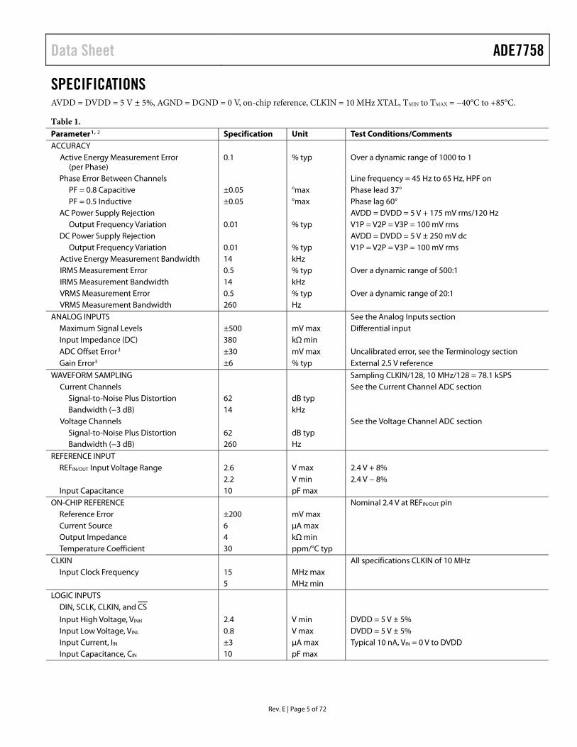
SPECIFICATIONS AVDD = DVDD = 5 V ± 5%, AGND = DGND = 0 V, on-chip reference, CLKIN = 10 MHz XTAL, TMIN to TMAX = −40°C to +85°C.
Table 1. Parameter1, 2 Specification Unit Test Conditions/Comments ACCURACY
Active Energy Measurement Error (per Phase)
0.1 % typ Over a dynamic range of 1000 to 1
Phase Error Between Channels Line frequency = 45 Hz to 65 Hz, HPF on PF = 0.8 Capacitive ±0.05 °max Phase lead 37° PF = 0.5 Inductive ±0.05 °max Phase lag 60°
AC Power Supply Rejection AVDD = DVDD = 5 V + 175 mV rms/120 Hz Output Frequency Variation 0.01 % typ V1P = V2P = V3P = 100 mV rms
DC Power Supply Rejection AVDD = DVDD = 5 V ± 250 mV dc Output Frequency Variation 0.01 % typ V1P = V2P = V3P = 100 mV rms
Active Energy Measurement Bandwidth 14 kHz IRMS Measurement Error 0.5 % typ Over a dynamic range of 500:1 IRMS Measurement Bandwidth 14 kHz VRMS Measurement Error 0.5 % typ Over a dynamic range of 20:1 VRMS Measurement Bandwidth 260 Hz
ANALOG INPUTS See the Analog Inputs section Maximum Signal Levels ±500 mV max Differential input Input Impedance (DC) 380 kΩ min ADC Offset Error3 ±30 mV max Uncalibrated error, see the Terminology section Gain Error3 ±6 % typ External 2.5 V reference
WAVEFORM SAMPLING Sampling CLKIN/128, 10 MHz/128 = 78.1 kSPS Current Channels See the Current Channel ADC section
Signal-to-Noise Plus Distortion 62 dB typ Bandwidth (−3 dB) 14 kHz
Voltage Channels See the Voltage Channel ADC section Signal-to-Noise Plus Distortion 62 dB typ Bandwidth (−3 dB) 260 Hz
REFERENCE INPUT REFIN/OUT Input Voltage Range 2.6 V max 2.4 V + 8% 2.2 V min 2.4 V − 8% Input Capacitance 10 pF max
ON-CHIP REFERENCE Nominal 2.4 V at REFIN/OUT pin Reference Error ±200 mV max Current Source 6 μA max Output Impedance 4 kΩ min Temperature Coefficient 30 ppm/°C typ
CLKIN All specifications CLKIN of 10 MHz Input Clock Frequency 15 MHz max
5 MHz min LOGIC INPUTS
DIN, SCLK, CLKIN, and CS
Input High Voltage, VINH 2.4 V min DVDD = 5 V ± 5% Input Low Voltage, VINL 0.8 V max DVDD = 5 V ± 5% Input Current, IIN ±3 μA max Typical 10 nA, VIN = 0 V to DVDD Input Capacitance, CIN 10 pF max

ADE7758 Data Sheet
Rev. E | Page 6 of 72
Parameter1, 2 Specification Unit Test Conditions/Comments LOGIC OUTPUTS DVDD = 5 V ± 5%
IRQ, DOUT, and CLKOUT IRQ is open-drain, 10 kΩ pull-up resistor
Output High Voltage, VOH 4 V min ISOURCE = 5 mA Output Low Voltage, VOL 0.4 V max ISINK = 1 mA
APCF and VARCF Output High Voltage, VOH 4 V min ISOURCE = 8 mA Output Low Voltage, VOL 1 V max ISINK = 5 mA
POWER SUPPLY For specified performance AVDD 4.75 V min 5 V − 5% 5.25 V max 5 V + 5% DVDD 4.75 V min 5 V − 5% 5.25 V max 5 V + 5% AIDD 8 mA max Typically 5 mA DIDD 13 mA max Typically 9 mA
1 See the Typical Performance Characteristics. 2 See the Terminology section for a definition of the parameters. 3 See the Analog Inputs section.
TIMING CHARACTERISTICS AVDD = DVDD = 5 V ± 5%, AGND = DGND = 0 V, on-chip reference, CLKIN = 10 MHz XTAL, TMIN to TMAX = −40°C to +85°C.
Table 2. Parameter1, 2 Specification Unit Test Conditions/Comments WRITE TIMING
t1 50 ns (min) CS falling edge to first SCLK falling edge
t2 50 ns (min) SCLK logic high pulse width t3 50 ns (min) SCLK logic low pulse width t4 10 ns (min) Valid data setup time before falling edge of SCLK t5 5 ns (min) Data hold time after SCLK falling edge t6 1200 ns (min) Minimum time between the end of data byte transfers t7 400 ns (min) Minimum time between byte transfers during a serial write t8 100 ns (min) CS hold time after SCLK falling edge
READ TIMING t9
3 4 μs (min) Minimum time between read command (that is, a write to communication register) and data read
t10 50 ns (min) Minimum time between data byte transfers during a multibyte read t11
4 30 ns (min) Data access time after SCLK rising edge following a write to the communications register t12
5 100 ns (max) Bus relinquish time after falling edge of SCLK 10 ns (min) t13
5 100 ns (max) Bus relinquish time after rising edge of CS
10 ns (min) 1 Sample tested during initial release and after any redesign or process change that may affect this parameter. All input signals are specified with tr = tf = 5 ns (10% to
90%) and timed from a voltage level of 1.6 V. 2 See the timing diagrams in Figure 3 and Figure 4 and the Serial Interface section. 3 Minimum time between read command and data read for all registers except waveform register, which is t9 = 500 ns min. 4 Measured with the load circuit in Figure 2 and defined as the time required for the output to cross 0.8 V or 2.4 V. 5 Derived from the measured time taken by the data outputs to change 0.5 V when loaded with the circuit in Figure 2. The measured number is then extrapolated back
to remove the effects of charging or discharging the 50 pF capacitor. This means that the time quoted here is the true bus relinquish time of the part and is independent of the bus loading.

Data Sheet ADE7758
Rev. E | Page 7 of 72
TIMING DIAGRAMS
200µA IOL
1.6mA IOH
2.1VTO OUTPUTPIN CL
50pF
0444
3-00
2
Figure 2. Load Circuit for Timing Specifications
DIN
SCLK
CS
t2
t3t1
t4 t5
t7
t6
t8
COMMAND BYTE MOST SIGNIFICANT BYTE LEAST SIGNIFICANT BYTE
1 A6 A4A5 A3 A2 A1 A0 DB7 DB0 DB7 DB0
t7
0444
3-00
3
Figure 3. Serial Write Timing
SCLK
CS
t1
t10
t13
0 A6 A4A5 A3 A2 A1 A0
DB0DB7 DB0DB7
DIN
DOUT
t11t12
COMMAND BYTE MOST SIGNIFICANT BYTE LEAST SIGNIFICANT BYTE
t9
0444
3-00
4
Figure 4. Serial Read Timing
ADE7758 Data Sheet
Rev. E | Page 8 of 72
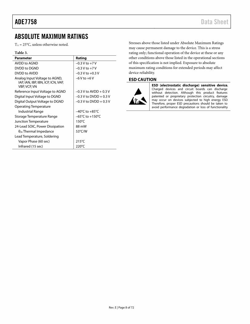
ABSOLUTE MAXIMUM RATINGS TA = 25°C, unless otherwise noted.
Table 3. Parameter Rating AVDD to AGND –0.3 V to +7 V DVDD to DGND –0.3 V to +7 V DVDD to AVDD –0.3 V to +0.3 V Analog Input Voltage to AGND,
IAP, IAN, IBP, IBN, ICP, ICN, VAP, VBP, VCP, VN
–6 V to +6 V
Reference Input Voltage to AGND –0.3 V to AVDD + 0.3 V Digital Input Voltage to DGND –0.3 V to DVDD + 0.3 V Digital Output Voltage to DGND –0.3 V to DVDD + 0.3 V Operating Temperature
Industrial Range –40°C to +85°C Storage Temperature Range –65°C to +150°C Junction Temperature 150°C 24-Lead SOIC, Power Dissipation 88 mW
θJA Thermal Impedance 53°C/W Lead Temperature, Soldering
Vapor Phase (60 sec) 215°C Infrared (15 sec) 220°C
Stresses above those listed under Absolute Maximum Ratings may cause permanent damage to the device. This is a stress rating only; functional operation of the device at these or any other conditions above those listed in the operational sections of this specification is not implied. Exposure to absolute maximum rating conditions for extended periods may affect device reliability.
ESD CAUTION
Data Sheet ADE7758
Rev. E | Page 9 of 72
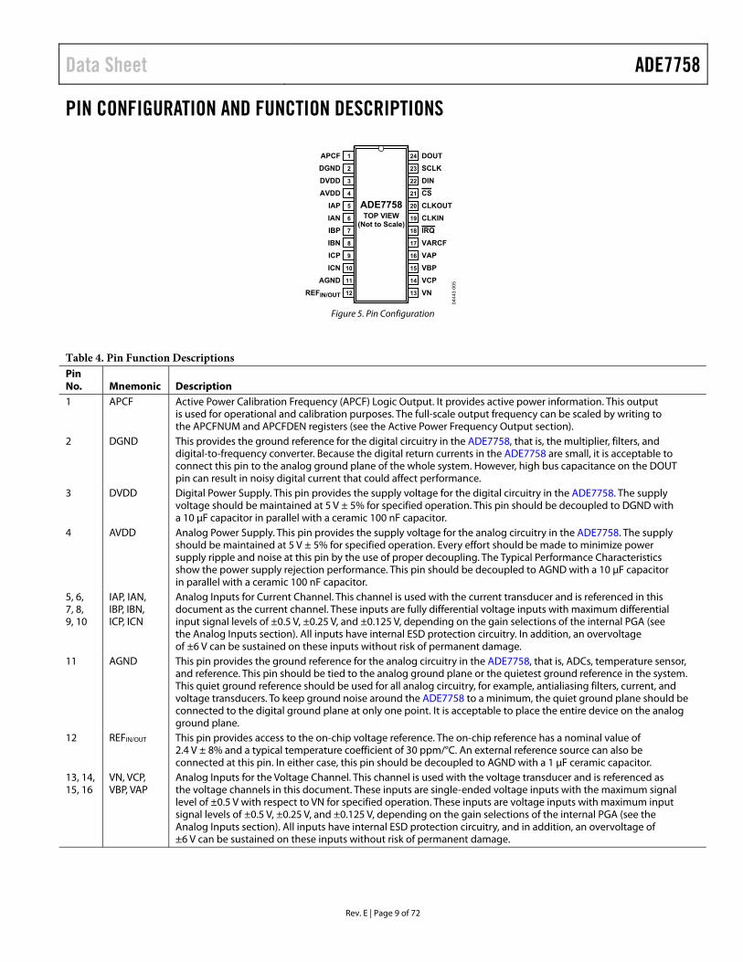
PIN CONFIGURATION AND FUNCTION DESCRIPTIONS
APCF 1
DGND 2
DVDD 3
AVDD 4
DOUT24
SCLK23
DIN22
CS21
IAP 5 CLKOUT20
IAN 6 CLKIN19
IBP 7 IRQ18
IBN 8 VARCF17
ICP 9 VAP16
ICN 10 VBP15
AGND 11 VCP14
REFIN/OUT 12 VN13
ADE7758TOP VIEW
(Not to Scale)
0444
3-00
5
Figure 5. Pin Configuration
Table 4. Pin Function Descriptions Pin No. Mnemonic Description 1 APCF Active Power Calibration Frequency (APCF) Logic Output. It provides active power information. This output
is used for operational and calibration purposes. The full-scale output frequency can be scaled by writing to the APCFNUM and APCFDEN registers (see the Active Power Frequency Output section).
2 DGND This provides the ground reference for the digital circuitry in the ADE7758, that is, the multiplier, filters, and digital-to-frequency converter. Because the digital return currents in the ADE7758 are small, it is acceptable to connect this pin to the analog ground plane of the whole system. However, high bus capacitance on the DOUT pin can result in noisy digital current that could affect performance.
3 DVDD Digital Power Supply. This pin provides the supply voltage for the digital circuitry in the ADE7758. The supply voltage should be maintained at 5 V ± 5% for specified operation. This pin should be decoupled to DGND with a 10 μF capacitor in parallel with a ceramic 100 nF capacitor.
4 AVDD Analog Power Supply. This pin provides the supply voltage for the analog circuitry in the ADE7758. The supply should be maintained at 5 V ± 5% for specified operation. Every effort should be made to minimize power supply ripple and noise at this pin by the use of proper decoupling. The Typical Performance Characteristics show the power supply rejection performance. This pin should be decoupled to AGND with a 10 μF capacitor in parallel with a ceramic 100 nF capacitor.
5, 6, 7, 8, 9, 10
IAP, IAN, IBP, IBN, ICP, ICN
Analog Inputs for Current Channel. This channel is used with the current transducer and is referenced in this document as the current channel. These inputs are fully differential voltage inputs with maximum differential input signal levels of ±0.5 V, ±0.25 V, and ±0.125 V, depending on the gain selections of the internal PGA (see the Analog Inputs section). All inputs have internal ESD protection circuitry. In addition, an overvoltage of ±6 V can be sustained on these inputs without risk of permanent damage.
11 AGND This pin provides the ground reference for the analog circuitry in the ADE7758, that is, ADCs, temperature sensor, and reference. This pin should be tied to the analog ground plane or the quietest ground reference in the system. This quiet ground reference should be used for all analog circuitry, for example, antialiasing filters, current, and voltage transducers. To keep ground noise around the ADE7758 to a minimum, the quiet ground plane should be connected to the digital ground plane at only one point. It is acceptable to place the entire device on the analog ground plane.
12 REFIN/OUT This pin provides access to the on-chip voltage reference. The on-chip reference has a nominal value of 2.4 V ± 8% and a typical temperature coefficient of 30 ppm/°C. An external reference source can also be connected at this pin. In either case, this pin should be decoupled to AGND with a 1 μF ceramic capacitor.
13, 14, 15, 16
VN, VCP, VBP, VAP
Analog Inputs for the Voltage Channel. This channel is used with the voltage transducer and is referenced as the voltage channels in this document. These inputs are single-ended voltage inputs with the maximum signal level of ±0.5 V with respect to VN for specified operation. These inputs are voltage inputs with maximum input signal levels of ±0.5 V, ±0.25 V, and ±0.125 V, depending on the gain selections of the internal PGA (see the Analog Inputs section). All inputs have internal ESD protection circuitry, and in addition, an overvoltage of ±6 V can be sustained on these inputs without risk of permanent damage.
ADE7758 Data Sheet
Rev. E | Page 10 of 72
Pin No. Mnemonic Description 17 VARCF Reactive Power Calibration Frequency Logic Output. It gives reactive power or apparent power information
depending on the setting of the VACF bit of the WAVMODE register. This output is used for operational and calibration purposes. The full-scale output frequency can be scaled by writing to the VARCFNUM and VARCFDEN registers (see the Reactive Power Frequency Output section).
18 IRQ Interrupt Request Output. This is an active low open-drain logic output. Maskable interrupts include: an active energy register at half level, an apparent energy register at half level, and waveform sampling up to 26 kSPS (see the Interrupts section).
19 CLKIN Master Clock for ADCs and Digital Signal Processing. An external clock can be provided at this logic input. Alternatively, a parallel resonant AT crystal can be connected across CLKIN and CLKOUT to provide a clock source for the ADE7758. The clock frequency for specified operation is 10 MHz. Ceramic load capacitors of a few tens of picofarad should be used with the gate oscillator circuit. Refer to the crystal manufacturer’s data sheet for the load capacitance requirements
20 CLKOUT A crystal can be connected across this pin and CLKIN as previously described to provide a clock source for the ADE7758. The CLKOUT pin can drive one CMOS load when either an external clock is supplied at CLKIN or a crystal is being used.
21 CS Chip Select. Part of the 4-wire serial interface. This active low logic input allows the ADE7758 to share the serial bus with several other devices (see the Serial Interface section).
22 DIN Data Input for the Serial Interface. Data is shifted in at this pin on the falling edge of SCLK (see the Serial Interface section).
23 SCLK Serial Clock Input for the Synchronous Serial Interface. All serial data transfers are synchronized to this clock (see the Serial Interface section). The SCLK has a Schmidt-trigger input for use with a clock source that has a slow edge transition time, for example, opto-isolator outputs.
24 DOUT Data Output for the Serial Interface. Data is shifted out at this pin on the rising edge of SCLK. This logic output is normally in a high impedance state, unless it is driving data onto the serial data bus (see the Serial Interface section).

Data Sheet ADE7758
Rev. E | Page 11 of 72
TERMINOLOGY Measurement Error The error associated with the energy measurement made by the ADE7758 is defined by
%100–
×
=
EnergyTrueEnergyTrueADE7758byRegisteredEnergy
ErrortMeasuremen
(1)
Phase Error Between Channels The high-pass filter (HPF) and digital integrator introduce a slight phase mismatch between the current and the voltage channel. The all-digital design ensures that the phase matching between the current channels and voltage channels in all three phases is within ±0.1° over a range of 45 Hz to 65 Hz and ±0.2° over a range of 40 Hz to 1 kHz. This internal phase mismatch can be combined with the external phase error (from current sensor or component tolerance) and calibrated with the phase calibration registers.
Power Supply Rejection (PSR) This quantifies the ADE7758 measurement error as a percentage of reading when the power supplies are varied. For the ac PSR measurement, a reading at nominal supplies (5 V) is taken. A second reading is obtained with the same input signal levels when an ac signal (175 mV rms/100 Hz) is introduced onto the supplies. Any error introduced by this ac signal is expressed as a percentage of reading—see the Measurement Error definition.
For the dc PSR measurement, a reading at nominal supplies (5 V) is taken. A second reading is obtained with the same input signal levels when the power supplies are varied ±5%. Any error introduced is again expressed as a percentage of the reading.
ADC Offset Error This refers to the dc offset associated with the analog inputs to the ADCs. It means that with the analog inputs connected to AGND that the ADCs still see a dc analog input signal. The magnitude of the offset depends on the gain and input range selection (see the Typical Performance Characteristics section). However, when HPFs are switched on, the offset is removed from the current channels and the power calculation is not affected by this offset.
Gain Error The gain error in the ADCs of the ADE7758 is defined as the difference between the measured ADC output code (minus the offset) and the ideal output code (see the Current Channel ADC section and the Voltage Channel ADC section). The difference is expressed as a percentage of the ideal code.
Gain Error Match The gain error match is defined as the gain error (minus the offset) obtained when switching between a gain of 1, 2, or 4. It is expressed as a percentage of the output ADC code obtained under a gain of 1.

ADE7758 Data Sheet
Rev. E | Page 12 of 72
TYPICAL PERFORMANCE CHARACTERISTICS 0.5
–0.5
–0.4
–0.3
–0.2
–0.1
0
0.1
0.2
0.3
0.4
0.01 0.1 1 10 100PERCENT FULL-SCALE CURRENT (%)
PER
CEN
T ER
RO
R (%
)
+25°C
PF = 1
+85°C
–40°C
0444
3-00
6
Figure 6. Active Energy Error as a Percentage of Reading (Gain = +1) over
Temperature with Internal Reference and Integrator Off
0.3
–0.3
–0.2
–0.1
0
0.1
0.2
0.01 0.1 1 10 100PERCENT FULL-SCALE CURRENT (%)
PER
CEN
T ER
RO
R (%
)
PF = +1, +25°CPF = +0.5, +25°C
PF = –0.5, +25°CPF = +0.5, +85°C
PF = +0.5, –40°C
0444
3-00
7
Figure 7. Active Energy Error as a Percentage of Reading (Gain = +1) over
Power Factor with Internal Reference and Integrator Off
0.3
–0.3
–0.2
–0.1
0
0.1
0.2
0.01 0.1 1 10 100PERCENT FULL-SCALE CURRENT (%)
PER
CEN
T ER
RO
R (%
)
GAIN = +2
GAIN = +4
PF = 1
GAIN = +1
0444
3-00
8
Figure 8. Active Energy Error as a Percentage of Reading over Gain with Internal Reference and Integrator Off
0.20
–0.20
–0.15
–0.10
–0.05
0
0.05
0.10
0.15
0.01 0.1 1 10 100PERCENT FULL-SCALE CURRENT (%)
PER
CEN
T ER
RO
R (%
)
PF = –0.5, +25°C
PF = +0.5, +25°C
PF = +0.5, –40°C
PF = +0.5, +85°C
0444
3-00
9
Figure 9. Active Energy Error as a Percentage of Reading (Gain = +1) over Temperature with External Reference and Integrator Off
0.5
0.6
–0.2
–0.3
–0.4
–0.1
0
0.1
0.2
0.3
0.4
45 47 49 51 53 55 57 59 61 63 65LINE FREQUENCY (Hz)
PER
CEN
T ER
RO
R (%
)W
ITH
RES
PEC
T TO
55H
z PF = 1
PF = 0.5
0444
3-01
0
Figure 10. Active Energy Error as a Percentage of Reading (Gain = +1) over Frequency with Internal Reference and Integrator Off
0.08
0.10
–0.06
–0.08
–0.10
–0.04
–0.02
0
0.02
0.04
0.06
0.01 0.1 1 10 100PERCENT FULL-SCALE CURRENT (%)
PER
CEN
T ER
RO
R (%
)W
ITH
RES
PEC
TTO
5V;
3A
VDD = 5V
VDD = 5.25V
VDD = 4.75V
PF = 1
0444
3-01
1
Figure 11. Active Energy Error as a Percentage of Reading (Gain = +1) over Power Supply with Internal Reference and Integrator Off

Data Sheet ADE7758
Rev. E | Page 13 of 72
0.20
0.25
–0.15
–0.20
–0.25
–0.10
–0.05
0
0.05
0.10
0.15
0.01 0.1 1 10 100PERCENT FULL-SCALE CURRENT (%)
PER
CEN
T ER
RO
R (%
)
PHASE A
PHASE B PHASE C
ALL PHASES
PF = 1
0444
3-01
2
Figure 12. APCF Error as a Percentage of Reading (Gain = +1)
with Internal Reference and Integrator Off
0.4
–0.4
–0.3
–0.2
–0.1
0
0.1
0.2
0.3
0.01 0.1 1 10 100
PF = 0, +25°C
PF = 0, +85°C
PF = 0, –40°C
PERCENT FULL-SCALE CURRENT (%)
PER
CEN
T ER
RO
R (%
)
0444
3-01
3
Figure 13. Reactive Energy Error as a Percentage of Reading (Gain = +1) over Temperature with Internal Reference and Integrator Off
0.8
–0.8
–0.6
–0.4
–0.2
0
0.2
0.4
0.6
0.01 0.1 1 10 100PERCENT FULL-SCALE CURRENT (%)
PER
CEN
T ER
RO
R (%
)
PF = 0, +25°C
PF = –0.866, +25°C
PF = +0.866, +25°C
PF = +0.866, +85°C
PF = +0.866, –40°C
0444
3-01
4
Figure 14. Reactive Energy Error as a Percentage of Reading (Gain = +1) over
Power Factor with Internal Reference and Integrator Off
0.3
–0.3
–0.2
–0.1
0
0.1
0.2
0.01 0.1 1 10 100PERCENT FULL-SCALE CURRENT (%)
PER
CEN
T ER
RO
R (%
)
PF = 0, +25°C
PF = 0, +85°C
PF = 0, –40°C
0444
3-01
5
Figure 15. Reactive Energy Error as a Percentage of Reading (Gain = +1) over
Temperature with External Reference and Integrator Off
0.3
–0.3
–0.2
–0.1
0
0.1
0.2
0.01 0.1 1 10 100PERCENT FULL-SCALE CURRENT (%)
PER
CEN
T ER
RO
R (%
)
PF = 0, +25°C
PF = –0.866, +25°C
PF = +0.866, +25°CPF = +0.866, +85°C
PF = +0.866, –40°C
0444
3-01
6
Figure 16. Reactive Energy Error as a Percentage of Reading (Gain = +1) over Power Factor with External Reference and Integrator Off
0.8
–0.8
–0.6
–0.4
–0.2
0
0.2
0.4
0.6
45 47 49 51 53 55 57 59 61 63 65LINE FREQUENCY (Hz)
PER
CEN
T ER
RO
R (%
)W
ITH
RES
PEC
T TO
55H
z PF = 0
PF = 0.866
0444
3-01
7
Figure 17. Reactive Energy Error as a Percentage of Reading (Gain = +1) over
Frequency with Internal Reference and Integrator Off
ADE7758 Data Sheet
Rev. E | Page 14 of 72
0.10
–0.10
–0.08
–0.06
–0.04
–0.02
0
0.02
0.04
0.06
0.08
0.01 0.1 1 10 100PERCENT FULL-SCALE CURRENT (%)
PER
CEN
T ER
RO
R (%
)W
ITH
RES
PEC
T TO
5V;
3A
5V
5.25V
4.75V
0444
3-01
8
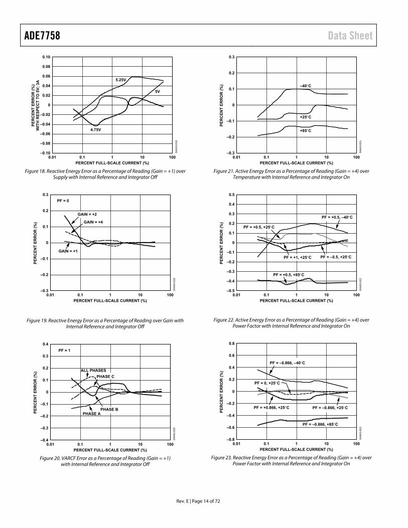
Figure 18. Reactive Energy Error as a Percentage of Reading (Gain = +1) over
Supply with Internal Reference and Integrator Off
0.3
–0.3
–0.2
–0.1
0
0.1
0.2
0.01 0.1 1 10 100PERCENT FULL-SCALE CURRENT (%)
PER
CEN
T ER
RO
R (%
)
GAIN = +1
GAIN = +2
GAIN = +4
PF = 0
0444
3-01
9
Figure 19. Reactive Energy Error as a Percentage of Reading over Gain with Internal Reference and Integrator Off
0.4
–0.4
–0.2
–0.3
–0.1
0
0.1
0.2
0.3
0.01 0.1 1 10 100PERCENT FULL-SCALE CURRENT (%)
PER
CEN
T ER
RO
R (%
)
PHASE A
ALL PHASESPHASE C
PHASE B
PF = 1
0444
3-02
0
Figure 20. VARCF Error as a Percentage of Reading (Gain = +1)
with Internal Reference and Integrator Off
0.3
–0.3
–0.2
–0.1
0
0.1
0.2
0.01 0.1 1 10 100PERCENT FULL-SCALE CURRENT (%)
PER
CEN
T ER
RO
R (%
)
+25°C
+85°C
–40°C
0444
3-02
1
Figure 21. Active Energy Error as a Percentage of Reading (Gain = +4) over
Temperature with Internal Reference and Integrator On
0.5
0.4
–0.5
–0.4
–0.2
–0.3
–0.1
0
0.1
0.2
0.3
0.01 0.1 1 10 100PERCENT FULL-SCALE CURRENT (%)
PER
CEN
T ER
RO
R (%
)
PF = +1, +25°C PF = –0.5, +25°C
PF = +0.5, +25°C
PF = +0.5, +85°C
PF = +0.5, –40°C
0444
3-02
2
Figure 22. Active Energy Error as a Percentage of Reading (Gain = +4) over Power Factor with Internal Reference and Integrator On
0.8
–0.8
–0.4
–0.6
–0.2
0
0.2
0.4
0.6
0.01 0.1 1 10 100PERCENT FULL-SCALE CURRENT (%)
PER
CEN
T ER
RO
R (%
)
PF = 0, +25°C
PF = +0.866, +25°C PF = –0.866, +25°C
PF = –0.866, +85°C
PF = –0.866, –40°C04
443-
023
Figure 23. Reactive Energy Error as a Percentage of Reading (Gain = +4) over
Power Factor with Internal Reference and Integrator On

Data Sheet ADE7758
Rev. E | Page 15 of 72
0.4
–0.5
–0.4
–0.2
–0.3
–0.1
0
0.1
0.2
0.3
0.01 0.1 1 10 100PERCENT FULL-SCALE CURRENT (%)
PER
CEN
T ER
RO
R (%
)
+25°C
+85°C
–40°C
PF = 0
0444
3-02
4
Figure 24. Reactive Energy Error as a Percentage of Reading (Gain = +4) over
Temperature with Internal Reference and Integrator On
0.5
0.4
–0.5
–0.4
–0.2
–0.3
–0.1
0
0.1
0.2
0.3
45 47 49 51 53 55 57 59 61 63 65LINE FREQUENCY (Hz)
PER
CEN
T ER
RO
R (%
)
PF = 1
PF = 0.5
0444
3-02
5
Figure 25. Active Energy Error as a Percentage of Reading (Gain = +4) over Frequency with Internal Reference and Integrator On
1.2
1.0
–0.8
–0.6
–0.2
–0.4
0
0.2
0.4
0.6
0.8
45 47 49 51 53 55 57 59 61 63 65LINE FREQUENCY (Hz)
PER
CEN
T ER
RO
R (%
)
PF = 0.866
PF = 0
0444
3-02
6
Figure 26. Reactive Energy Error as a Percentage of Reading (Gain = +4) over
Frequency with Internal Reference and Integrator On
0.8
0.6
–1.2
–1.0
–0.6
–0.8
–0.4
–0.2
0
0.2
0.4
0.01 0.1 1 10 100
PF = 0.5
PERCENT FULL-SCALE CURRENT (%)
PER
CEN
T ER
RO
R (%
)
PF = 1
0444
3-02
7
Figure 27. IRMS Error as a Percentage of Reading (Gain = +1)
with Internal Reference and Integrator Off
0.8
0.6
–1.0
–0.6
–0.8
–0.4
–0.2
0
0.2
0.4
0.1 1 10 100
PF = +1
PF = –0.5
PERCENT FULL-SCALE CURRENT (%)
PER
CEN
T ER
RO
R (%
)
0444
3-02
8
Figure 28. IRMS Error as a Percentage of Reading (Gain = +4) with Internal Reference and Integrator On
0.4
–0.4
–0.3
–0.2
–0.1
0
0.1
0.2
0.3
1 10 100VOLTAGE (V)
PER
CEN
T ER
RO
R (%
)
0444
3-02
9
Figure 29. VRMS Error as a Percentage of Reading (Gain = +1)
with Internal Reference
ADE7758 Data Sheet
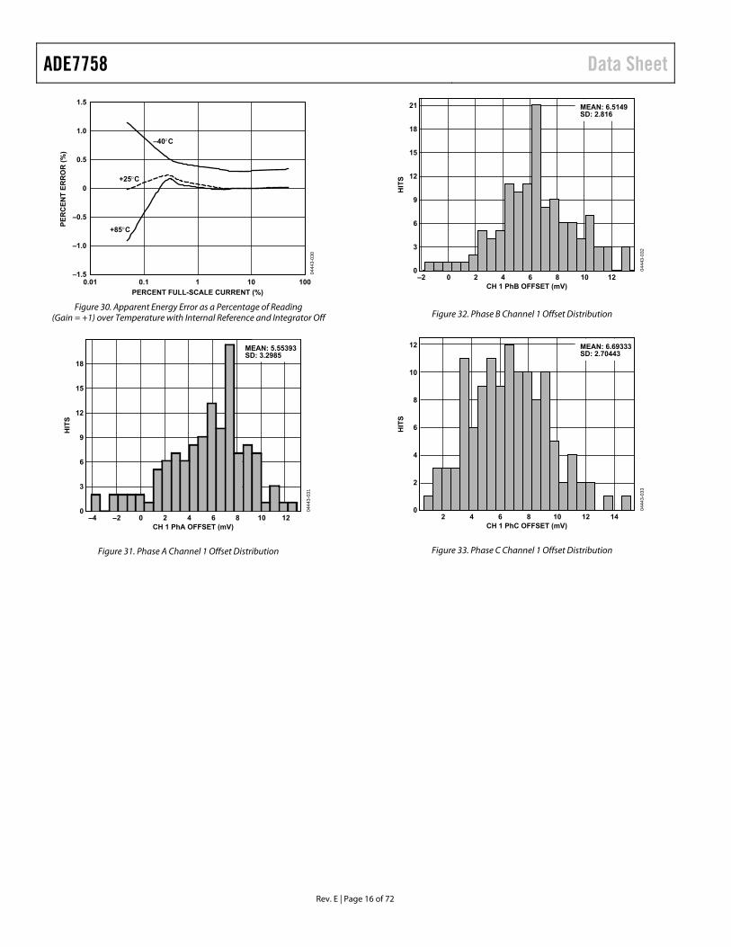
Rev. E | Page 16 of 72
1.5
–1.5
–1.0
–0.5
0
0.5
1.0
0.01 1 100.1 100
+25°C
+85°C
–40°C
PERCENT FULL-SCALE CURRENT (%)
PER
CEN
T ER
RO
R (%
)
0444
3-03
0
–2 0 2 4 6 8 10 12
18
21
15
12
9
6
3
0
CH 1 PhB OFFSET (mV)
HIT
S
MEAN: 6.5149SD: 2.816
0444
3-03
2
Figure 30. Apparent Energy Error as a Percentage of Reading (Gain = +1) over Temperature with Internal Reference and Integrator Off Figure 32. Phase B Channel 1 Offset Distribution
2 4 6 8 10 1412
12
10
8
6
4
2
0
CH 1 PhC OFFSET (mV)
HIT
S
MEAN: 6.69333SD: 2.70443
0444
3-03
3
–4 –2 0 2 4 6 8 10 12
18
15
12
9
6
3
0
CH 1 PhA OFFSET (mV)
HIT
S
MEAN: 5.55393SD: 3.2985
0444
3-03
1
Figure 33. Phase C Channel 1 Offset Distribution Figure 31. Phase A Channel 1 Offset Distribution

Data Sheet ADE7758
Rev. E | Page 17 of 72
TEST CIRCUITS
REFIN/OUT
33nF
1kΩ
100nF
33nF
1kΩ
10µF
VDD
VN
IAN
IBP
IBN
ICP
ICN
VAP
AVDD DVDD
VBP
VCPAGND DGND
DOUT
SCLK
APCF
CLKOUT
CLKIN
CS
DINIRQ
10MHz
22pF
22pF
PS2501-1
13 11 2
1
TO FREQ.COUNTER
1 4
2 3
20
IAP
RB
SAME ASIAP, IAN
9
8
7
10
16
15
14 100nF 10µF
33nF1kΩ
1MΩ
220V
33nF
1kΩ
825ΩI
TO SPI BUS
34
19
5
6
24
23
21
22
18
12
SAME ASIAP, IAN
SAME AS VAP
SAME AS VAP
ADE7758
CURRENTTRANSFORMER
17
VARCF
CT TURN RATIO 1800:1CHANNEL 2 GAIN = +1
CHANNEL 1 GAIN RB1 10Ω2 5Ω4 2.5Ω8 1.25Ω 04
443-
034
Figure 34. Test Circuit for Integrator Off
REFIN/OUT
33nF
1kΩ
33nF
1kΩ
33nF
1kΩ
33nF
1kΩ
100nF10µF
VDD
VN
IAN
IBP
IBN
ICP
ICN
VAP
AVDD DVDD
VBP
VCPAGND DGND
DOUT
SCLK
APCF
CLKOUT
CLKIN
CS
DINIRQ
10MHz
22pF
22pF
PS2501-1
13 11 2
1
TO FREQ.COUNTER
1 4
2 3
20
IAP
SAME ASIAP, IAN
9
8
7
10
16
15
14 100nF 10µF
33nF1kΩ
1MΩ
220V
33nF
1kΩ
825Ω
TO SPI BUS
34
19
5
6
24
23
21
22
18
12
SAME ASIAP, IAN
SAME AS VAP
SAME AS VAP
ADE7758
Idi/dt SENSOR 17
VARCF
CHANNEL 1 GAIN = +8CHANNEL 2 GAIN = +1
0444
3-03
5
Figure 35. Test Circuit for Integrator On

ADE7758 Data Sheet
Rev. E | Page 18 of 72
THEORY OF OPERATION ANTIALIASING FILTER This filter prevents aliasing, which is an artifact of all sampled systems. Input signals with frequency components higher than half the ADC sampling rate distort the sampled signal at a fre-quency below half the sampling rate. This happens with all ADCs, regardless of the architecture. The combination of the high sampling rate ∑-Δ ADC used in the ADE7758 with the relatively low bandwidth of the energy meter allows a very simple low-pass filter (LPF) to be used as an antialiasing filter. A simple RC filter (single pole) with a corner frequency of 10 kHz produces an attenuation of approximately 40 dB at 833 kHz. This is usually sufficient to eliminate the effects of aliasing.
ANALOG INPUTS The ADE7758 has six analog inputs divided into two channels: current and voltage. The current channel consists of three pairs of fully differential voltage inputs: IAP and IAN, IBP and IBN, and ICP and ICN. These fully differential voltage input pairs have a maximum differential signal of ±0.5 V. The current channel has a programmable gain amplifier (PGA) with possible gain selection of 1, 2, or 4. In addition to the PGA, the current channels also have a full-scale input range selection for the ADC. The ADC analog input range selection is also made using the gain register (see Figure 38). As mentioned previously, the maximum differential input voltage is ±0.5 V. However, by using Bit 3 and Bit 4 in the gain register, the maximum ADC input voltage can be set to ±0.5 V, ±0.25 V, or ±0.125 V on the current channels. This is achieved by adjusting the ADC reference (see the Reference Circuit section).
Figure 36 shows the maximum signal levels on the current channel inputs. The maximum common-mode signal is ±25 mV, as shown in Figure 37.
DIFFERENTIAL INPUTV1 + V2 = 500mV MAX PEAK
+500mV
VCM
V1
IAP, IBP,OR ICP
VCM
–500mV
COMMON-MODE±25mV MAX
V1 + V2
V2 IAN, IBN,OR ICN
0444
3-03
6
Figure 36. Maximum Signal Levels, Current Channels, Gain = 1
The voltage channel has three single-ended voltage inputs: VAP, VBP, and VCP. These single-ended voltage inputs have a maximum input voltage of ±0.5 V with respect to VN. Both the current and voltage channel have a PGA with possible gain selections of 1, 2, or 4. The same gain is applied to all the inputs of each channel.
Figure 37 shows the maximum signal levels on the voltage channel inputs. The maximum common-mode signal is ±25 mV, as shown in Figure 36.
SINGLE-ENDED INPUT±500mV MAX PEAK
+500mV
AGND
VCM
V2
VAP, VBP,OR VCP
VCM
–500mV
COMMON-MODE±25mV MAX
VN
V2
0444
3-03
7
Figure 37. Maximum Signal Levels, Voltage Channels, Gain = 1
The gain selections are made by writing to the gain register. Bit 0 to Bit 1 select the gain for the PGA in the fully differential current channel. The gain selection for the PGA in the single-ended voltage channel is made via Bit 5 to Bit 6. Figure 38 shows how a gain selection for the current channel is made using the gain register.
IAP, IBP, ICP
IAN, IBN, ICN
VIN K × VIN
GAIN[7:0]
GAIN (K)SELECTION
0444
3-03
8
Figure 38. PGA in Current Channel
Figure 39 shows how the gain settings in PGA 1 (current channel) and PGA 2 (voltage channel) are selected by various bits in the gain register.
GAIN REGISTER1CURRENT AND VOLTAGE CHANNEL PGA CONTROL
7 6 5 4 3 2 1 0
0 0 0 0 0 0 0 0 ADDRESS: 0x23
RESERVED
1REGISTER CONTENTS SHOW POWER-ON DEFAULTS
PGA 2 GAIN SELECT00 = ×101 = ×210 = ×4
INTEGRATOR ENABLE0 = DISABLE1 = ENABLE
PGA 1 GAIN SELECT00 = ×101 = ×210 = ×4
CURRENT INPUT FULL-SCALE SELECT00 = 0.5V01 = 0.25V10 = 0.125V
0444
3-03
9
Figure 39. Analog Gain Register
Bit 7 of the gain register is used to enable the digital integrator in the current signal path. Setting this bit activates the digital integrator (see the DI/DT Current Sensor and Digital Integrator section).

Data Sheet ADE7758
Rev. E | Page 19 of 72
CURRENT CHANNEL ADC Figure 41 shows the ADC and signal processing path for the input IA of the current channels (same for IB and IC). In waveform sampling mode, the ADC outputs are signed twos complement 24-bit data-words at a maximum of 26.0 kSPS (thousand samples per second). With the specified full-scale analog input signal of ±0.5 V, the ADC produces its maximum output code value (see Figure 41). This diagram shows a full-scale voltage signal being applied to the differential inputs IAP and IAN. The ADC output swings between 0xD7AE14 (−2,642,412) and 0x2851EC (+2,642,412).
Current Channel Sampling
The waveform samples of the current channel can be routed to the WFORM register at fixed sampling rates by setting the WAVSEL[2:0] bit in the WAVMODE register to 000 (binary) (see Table 20). The phase in which the samples are routed is set by setting the PHSEL[1:0] bits in the WAVMODE register. Energy calculation remains uninterrupted during waveform sampling.
When in waveform sample mode, one of four output sample rates can be chosen by using Bit 5 and Bit 6 of the WAVMODE register (DTRT[1:0]). The output sample rate can be 26.04 kSPS, 13.02 kSPS, 6.51 kSPS, or 3.25 kSPS. By setting the WFSM bit in the interrupt mask register to Logic 1, the interrupt request output IRQ goes active low when a sample is available. The timing is shown in . The 24-bit waveform samples are transferred from the one byte (8-bits) at a time, with the most significant byte shifted out first.
Figure 40ADE7758
READ FROM WAVEFORM0
SGN
CURRENT CHANNEL DATA–24 BITS
0x12
SCLK
DIN
DOUT
IRQ
0444
3-04
0
Figure 40. Current Channel Waveform Sampling
The interrupt request output IRQ stays low until the interrupt routine reads the reset status register (see the section). Interrupts
DIGITALINTEGRATOR1
GAIN[7]
ADC
REFERENCE
ACTIVE AND REACTIVEPOWER CALCULATION
WAVEFORM SAMPLEREGISTER
CURRENT RMS (IRMS)CALCULATION
IAP
IAN
PGA1VIN
GAIN[4:3]2.42V, 1.21V, 0.6V
GAIN[1:0]×1, ×2, ×4
ANALOGINPUTRANGE
VIN
0V
0.5V/GAIN0.25V/GAIN0.125V/GAIN
ADC OUTPUTWORD RANGE
CHANNEL 1(CURRENT WAVEFORM)DATA RANGE
0xD7AE14
0x000000
0x2851EC
50HzCHANNEL 1 (CURRENT WAVEFORM)DATA RANGE AFTER INTEGRATOR(50Hz AND AIGAIN[11:0] = 0x000)
0xCB2E48
0x000000
0x34D1B8
60HzCHANNEL 1 (CURRENT WAVEFORM)DATA RANGE AFTER INTEGRATOR(60Hz AND AIGAIN[11:0] = 0x000)
0xD4176D
0x000000
0x2BE893
HPF
0444
3-04
11WHEN DIGITAL INTEGRATOR IS ENABLED, FULL-SCALE OUTPUT DATA ISATTENUATED DEPENDING ON THE SIGNAL FREQUENCY BECAUSE THE
INTEGRATOR HAS A –20dB/DECADE FREQUENCY RESPONSE. WHEN DISABLED, THE OUTPUT WILL NOT BE FURTHER ATTENUATED.
Figure 41. Current Channel Signal Path
ADE7758 Data Sheet
Rev. E | Page 20 of 72
DI/DT CURRENT SENSOR AND DIGITAL INTEGRATOR The di/dt sensor detects changes in the magnetic field caused by the ac current. Figure 42 shows the principle of a di/dt current sensor.
MAGNETIC FIELD CREATED BY CURRENT(DIRECTLY PROPORTIONAL TO CURRENT)
+ EMF (ELECTROMOTIVE FORCE)
– INDUCED BY CHANGES INMAGNETIC FLUX DENSITY (di/dt)
0444
3-04
2
Figure 42. Principle of a di/dt Current Sensor
The flux density of a magnetic field induced by a current is directly proportional to the magnitude of the current. The changes in the magnetic flux density passing through a conductor loop generate an electromotive force (EMF) between the two ends of the loop. The EMF is a voltage signal that is propor-tional to the di/dt of the current. The voltage output from the di/dt current sensor is determined by the mutual inductance between the current carrying conductor and the di/dt sensor.
The current signal needs to be recovered from the di/dt signal before it can be used. An integrator is therefore necessary to restore the signal to its original form. The ADE7758 has a built-in digital integrator to recover the current signal from the di/dt sensor. The digital integrator on Channel 1 is disabled by default when the ADE7758 is powered up. Setting the MSB of the GAIN[7:0] register turns on the integrator. Figure 43 to Figure 46 show the magnitude and phase response of the digital integrator.
10 100 1k 10k
20
–50
–40
–30
–20
–10
0
10
FREQUENCY (Hz)
GA
IN (
dB
)
0444
3-04
3
Figure 43. Combined Gain Response of the Digital Integrator and Phase Compensator
10 100 1k 10k
80
91
90
89
88
87
86
85
84
83
82
81
FREQUENCY (Hz)
PH
AS
E (
De
gre
es
)
0444
3-04
4
Figure 44. Combined Phase Response of the Digital Integrator and Phase Compensator
40 706560555045
5
–1
0
1
2
3
4
FREQUENCY (Hz)
MA
GN
ITU
DE
(d
B)
0444
3-04
5
Figure 45. Combined Gain Response of the
Digital Integrator and Phase Compensator (40 Hz to 70 Hz)
40 706560555045
89.80
90.10
90.05
90.00
89.95
89.90
89.85
FREQUENCY (Hz)
PH
AS
E (
De
gre
es
)
0444
3-04
6
Figure 46. Combined Phase Response of the
Digital Integrator and Phase Compensator (40 Hz to 70 Hz)

Data Sheet ADE7758
Rev. E | Page 21 of 72
Note that the integrator has a −20 dB/dec attenuation and approximately −90° phase shift. When combined with a di/dt sensor, the resulting magnitude and phase response should be a flat gain over the frequency band of interest. However, the di/dt sensor has a 20 dB/dec gain associated with it and generates significant high frequency noise. A more effective antialiasing filter is needed to avoid noise due to aliasing (see the Theory of Operation section).
When the digital integrator is switched off, the ADE7758 can be used directly with a conventional current sensor, such as a current transformer (CT) or a low resistance current shunt.
PEAK CURRENT DETECTION The ADE7758 can be programmed to record the peak of the current waveform and produce an interrupt if the current exceeds a preset limit.
Peak Current Detection Using the PEAK Register
The peak absolute value of the current waveform within a fixed number of half-line cycles is stored in the IPEAK register. Figure 47 illustrates the timing behavior of the peak current detection.
L2
L1
CONTENT OFIPEAK[7:0]
00 L1 L2 L1
NO. OF HALFLINE CYCLESSPECIFIED BYLINECYC[15:0]
REGISTER
CURRENT WAVEFORM(PHASE SELECTED BY
PEAKSEL[2:0] INMMODE REGISTER)
0444
3-04
7
Figure 47. Peak Current Detection Using the IPEAK Register
Note that the content of the IPEAK register is equivalent to Bit 14 to Bit 21 of the current waveform sample. At full-scale analog input, the current waveform sample is 0x2851EC. The IPEAK at full-scale input is therefore expected to be 0xA1.
In addition, multiple phases can be activated for the peak detection simultaneously by setting more than one of the PEAKSEL[2:4] bits in the MMODE register to logic high. These bits select the phase for both voltage and current peak measurements. Note that if more than one bit is set, the VPEAK and IPEAK registers can hold values from two different phases, that is, the voltage and current peak are independently processed (see the Peak Current Detection section).
Note that the number of half-line cycles is based on counting the zero crossing of the voltage channel. The ZXSEL[2:0] bits in the LCYCMODE register determine which voltage channels are used for the zero-crossing detection. The same signal is also used for line cycle energy accumulation mode if activated (see the Line Cycle Accumulation Mode Register (0X17) section).
OVERCURRENT DETECTION INTERRUPT Figure 48 illustrates the behavior of the overcurrent detection.
IPINTLVL[7:0]
READ RSTATUSREGISTER
PKI INTERRUPT FLAG(BIT 15 OF STATUS
REGISTER)
PKI RESET LOWWHEN RSTATUSREGISTER IS READ
CURRENT PEAK WAVEFORM BEING MONITORED(SELECTED BY PKIRQSEL[2:0] IN MMODE REGISTER)
0444
3-04
8
Figure 48. ADE7758 Overcurrent Detection
Note that the content of the IPINTLVL[7:0] register is equivalent to Bit 14 to Bit 21 of the current waveform sample. Therefore, setting this register to 0xA1 represents putting peak detection at full-scale analog input. Figure 48 shows a current exceeding a threshold. The overcurrent event is recorded by setting the PKI flag (Bit 15) in the interrupt status register. If the PKI enable bit is set to Logic 1 in the interrupt mask register, the IRQ logic output goes active low (see the Interrupts section).
Similar to peak level detection, multiple phases can be activated for peak detection. If any of the active phases produce waveform samples above the threshold, the PKI flag in the interrupt status register is set. The phase of which overcurrent is monitored is set by the PKIRQSEL[2:0] bits in the MMODE register (see Table 19).
ADE7758 Data Sheet
Rev. E | Page 22 of 72
ADCTO VOLTAGE RMSCALCULATION ANDWAVEFORM SAMPLING
TO ACTIVE ANDREACTIVE ENERGYCALCULATION
VAP+
–VN
PGAVA
GAIN[6:5]×1, ×2, ×4
LPF OUTPUTWORD RANGE
0xD869
0x0
0x2797
50Hz
LPF OUTPUTWORD RANGE
0xD8B8
0x0
0x2748
60Hz0xD7AE
0x0
0x2852
PHASECALIBRATION
PHCAL[6:0]Φ
ANALOG INPUTRANGE
VA
0V
0.5VGAIN
LPF1f3dB = 260Hz
0444
3-04
9
Figure 49. ADC and Signal Processing in Voltage Channel
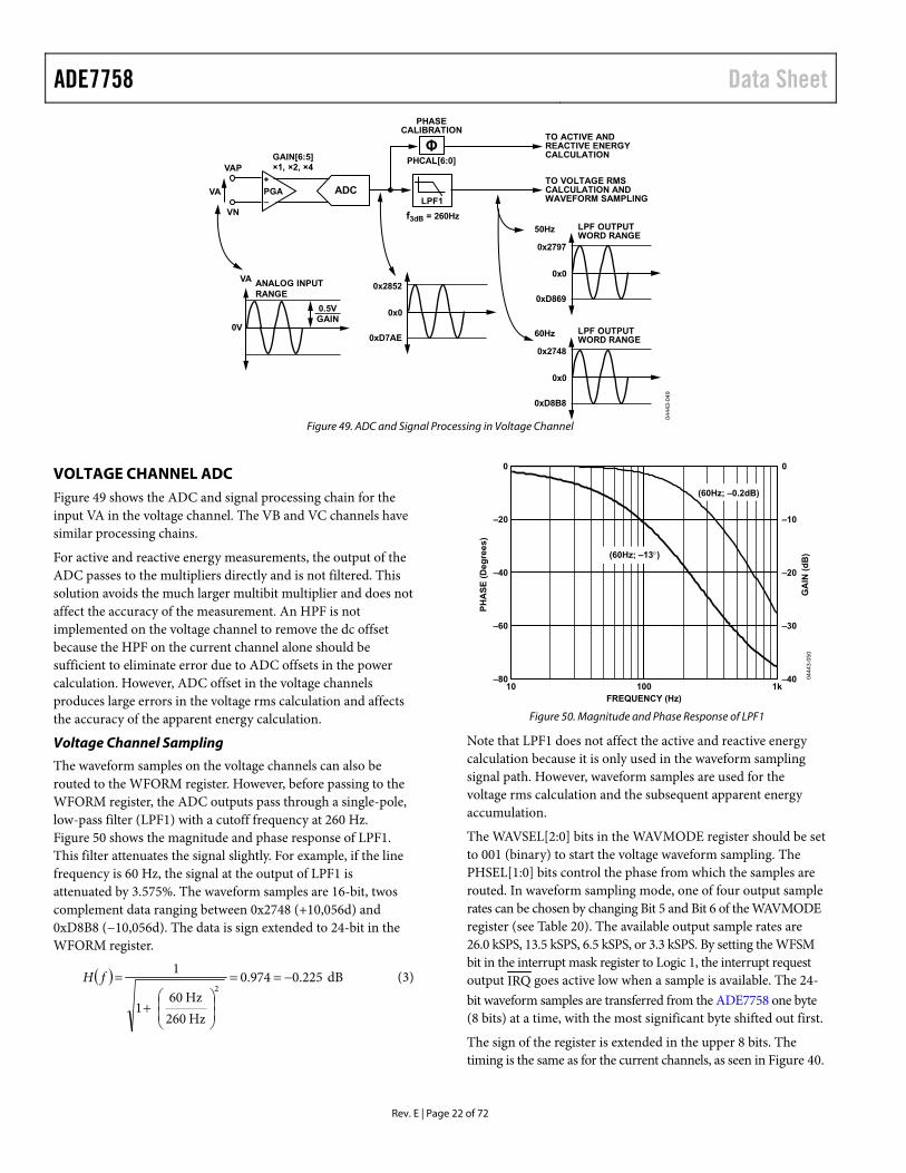
VOLTAGE CHANNEL ADC Figure 49 shows the ADC and signal processing chain for the input VA in the voltage channel. The VB and VC channels have similar processing chains.
For active and reactive energy measurements, the output of the ADC passes to the multipliers directly and is not filtered. This solution avoids the much larger multibit multiplier and does not affect the accuracy of the measurement. An HPF is not implemented on the voltage channel to remove the dc offset because the HPF on the current channel alone should be sufficient to eliminate error due to ADC offsets in the power calculation. However, ADC offset in the voltage channels produces large errors in the voltage rms calculation and affects the accuracy of the apparent energy calculation.
Voltage Channel Sampling
The waveform samples on the voltage channels can also be routed to the WFORM register. However, before passing to the WFORM register, the ADC outputs pass through a single-pole, low-pass filter (LPF1) with a cutoff frequency at 260 Hz. Figure 50 shows the magnitude and phase response of LPF1. This filter attenuates the signal slightly. For example, if the line frequency is 60 Hz, the signal at the output of LPF1 is attenuated by 3.575%. The waveform samples are 16-bit, twos complement data ranging between 0x2748 (+10,056d) and 0xD8B8 (−10,056d). The data is sign extended to 24-bit in the WFORM register.
( ) dB225.0974.0
Hz260Hz60
1
12
−==
⎟⎟⎠
⎞⎜⎜⎝
⎛+
=fH (3)
0
–20
–40
–60
–80
0
–10
–20
–30
–4010 100 1k
FREQUENCY (Hz)
PHA
SE (D
egre
es)
GA
IN (d
B)
(60Hz; –0.2dB)
(60Hz; –13°)
0444
3-05
0
Figure 50. Magnitude and Phase Response of LPF1
Note that LPF1 does not affect the active and reactive energy calculation because it is only used in the waveform sampling signal path. However, waveform samples are used for the voltage rms calculation and the subsequent apparent energy accumulation.
The WAVSEL[2:0] bits in the WAVMODE register should be set to 001 (binary) to start the voltage waveform sampling. The PHSEL[1:0] bits control the phase from which the samples are routed. In waveform sampling mode, one of four output sample rates can be chosen by changing Bit 5 and Bit 6 of the WAVMODE register (see Table 20). The available output sample rates are 26.0 kSPS, 13.5 kSPS, 6.5 kSPS, or 3.3 kSPS. By setting the WFSM bit in the interrupt mask register to Logic 1, the interrupt request output IRQ goes active low when a sample is available. The 24-bit waveform samples are transferred from the one byte (8 bits) at a time, with the most significant byte shifted out first.
ADE7758
The sign of the register is extended in the upper 8 bits. The timing is the same as for the current channels, as seen in Figure 40.
Data Sheet ADE7758
Rev. E | Page 23 of 72
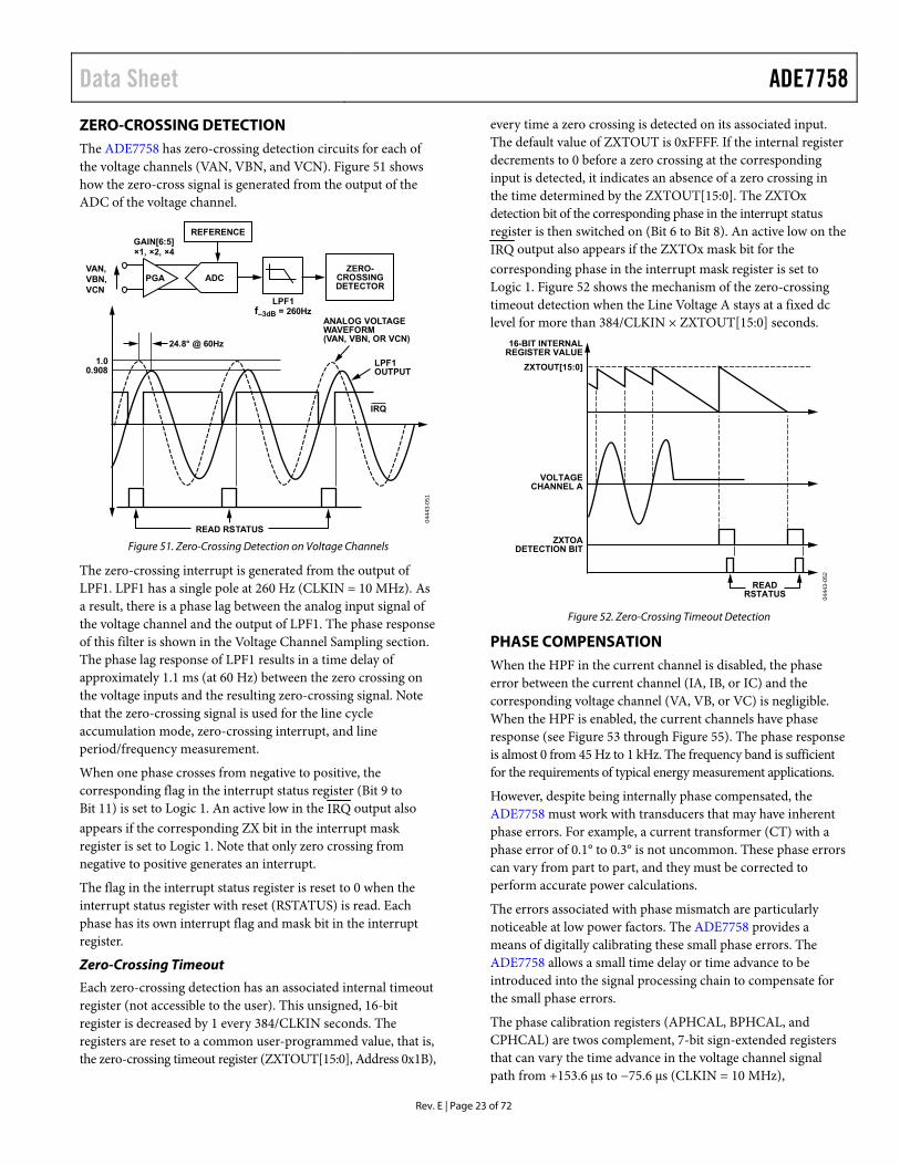
ZERO-CROSSING DETECTION The ADE7758 has zero-crossing detection circuits for each of the voltage channels (VAN, VBN, and VCN). Figure 51 shows how the zero-cross signal is generated from the output of the ADC of the voltage channel.
REFERENCE
ADCZERO-
CROSSINGDETECTOR
PGAVAN,VBN,VCN
GAIN[6:5]×1, ×2, ×4
LPF1f–3dB = 260Hz
24.8° @ 60Hz
ANALOG VOLTAGEWAVEFORM(VAN, VBN, OR VCN)
LPF1OUTPUT
READ RSTATUS
IRQ
1.00.908
0444
3-05
1
Figure 51. Zero-Crossing Detection on Voltage Channels
The zero-crossing interrupt is generated from the output of LPF1. LPF1 has a single pole at 260 Hz (CLKIN = 10 MHz). As a result, there is a phase lag between the analog input signal of the voltage channel and the output of LPF1. The phase response of this filter is shown in the Voltage Channel Sampling section. The phase lag response of LPF1 results in a time delay of approximately 1.1 ms (at 60 Hz) between the zero crossing on the voltage inputs and the resulting zero-crossing signal. Note that the zero-crossing signal is used for the line cycle accumulation mode, zero-crossing interrupt, and line period/frequency measurement.
When one phase crosses from negative to positive, the corresponding flag in the interrupt status register (Bit 9 to Bit 11) is set to Logic 1. An active low in the IRQ output also appears if the corresponding ZX bit in the interrupt mask register is set to Logic 1. Note that only zero crossing from negative to positive generates an interrupt.
The flag in the interrupt status register is reset to 0 when the interrupt status register with reset (RSTATUS) is read. Each phase has its own interrupt flag and mask bit in the interrupt register.
Zero-Crossing Timeout
Each zero-crossing detection has an associated internal timeout register (not accessible to the user). This unsigned, 16-bit register is decreased by 1 every 384/CLKIN seconds. The registers are reset to a common user-programmed value, that is, the zero-crossing timeout register (ZXTOUT[15:0], Address 0x1B),
every time a zero crossing is detected on its associated input. The default value of ZXTOUT is 0xFFFF. If the internal register decrements to 0 before a zero crossing at the corresponding input is detected, it indicates an absence of a zero crossing in the time determined by the ZXTOUT[15:0]. The ZXTOx detection bit of the corresponding phase in the interrupt status register is then switched on (Bit 6 to Bit 8). An active low on the IRQ output also appears if the ZXTOx mask bit for the corresponding phase in the interrupt mask register is set to Logic 1. shows the mechanism of the zero-crossing timeout detection when the Line Voltage A stays at a fixed dc level for more than 384/CLKIN × ZXTOUT[15:0] seconds.
Figure 52
ZXTOADETECTION BIT
READRSTATUS
VOLTAGECHANNEL A
ZXTOUT[15:0]
16-BIT INTERNALREGISTER VALUE
0444
3-05
2
Figure 52. Zero-Crossing Timeout Detection
PHASE COMPENSATION When the HPF in the current channel is disabled, the phase error between the current channel (IA, IB, or IC) and the corresponding voltage channel (VA, VB, or VC) is negligible. When the HPF is enabled, the current channels have phase response (see Figure 53 through Figure 55). The phase response is almost 0 from 45 Hz to 1 kHz. The frequency band is sufficient for the requirements of typical energy measurement applications.
However, despite being internally phase compensated, the ADE7758 must work with transducers that may have inherent phase errors. For example, a current transformer (CT) with a phase error of 0.1° to 0.3° is not uncommon. These phase errors can vary from part to part, and they must be corrected to perform accurate power calculations.
The errors associated with phase mismatch are particularly noticeable at low power factors. The ADE7758 provides a means of digitally calibrating these small phase errors. The ADE7758 allows a small time delay or time advance to be introduced into the signal processing chain to compensate for the small phase errors.
The phase calibration registers (APHCAL, BPHCAL, and CPHCAL) are twos complement, 7-bit sign-extended registers that can vary the time advance in the voltage channel signal path from +153.6 μs to −75.6 μs (CLKIN = 10 MHz),
ADE7758 Data Sheet
Rev. E | Page 24 of 72
40 706560555045
0.20
0.15
0.10
0.05
0
–0.05
–0.10
FREQUENCY (Hz)
PHA
SE (D
egre
es)
0444
3-05
4
respectively. Negative values written to the PHCAL registers represent a time advance, and positive values represent a time delay. One LSB is equivalent to 1.2 μs of time delay or 2.4 μs of time advance with a CLKIN of 10 MHz. With a line frequency of 60 Hz, this gives a phase resolution of 0.026° (360° × 1.2 μs × 60 Hz) at the fundamental in the positive direction (delay) and 0.052° in the negative direction (advance). This corresponds to a total correction range of −3.32° to +1.63° at 60 Hz.
Figure 56 illustrates how the phase compensation is used to remove a 0.1° phase lead in IA of the current channel from the external current transducer. To cancel the lead (0.1°) in the current channel of Phase A, a phase lead must be introduced into the corresponding voltage channel. The resolution of the phase adjustment allows the introduction of a phase lead of 0.104°. The phase lead is achieved by introducing a time advance into VA. A time advance of 4.8 μs is made by writing −2 (0x7E) to the time delay block (APHCAL[6:0]), thus reducing the amount of time delay by 4.8 μs or equivalently, 360° × 4.8 μs × 60 Hz = 0.104° at 60 Hz.
Figure 54. Phase Response of the HPF and Phase Compensation (40 Hz to 70 Hz)
44 565452504846
0.10
0.08
0.06
0.04
0.02
0
–0.02
FREQUENCY (Hz)
PHA
SE (D
egre
es)
0444
3-05
5
0 100 200 300 400 500 600 700 800 1k900
90
0
10
20
30
40
50
60
70
80
FREQUENCY (Hz)
PHA
SE (D
egre
es)
0444
3-05
3
Figure 55. Phase Response of HPF and Phase Compensation (44 Hz to 56 Hz)
Figure 53. Phase Response of the HPF and Phase Compensation (10 Hz to 1 kHz)

Data Sheet ADE7758
Rev. E | Page 25 of 72
PGA1
IAP
IAN
IA ADC
HPF
PGA2
VAP
VN
VA ADC
60Hz
0.1°IA
VA
RANGE OF PHASECALIBRATION
1 1 1 1 1 0 06 0
APHCAL[6:0]–153.6µs TO +75.6µs
VA VA ADVANCED BY 4.8µs(+0.104° @ 60Hz)
0x7EIA
60Hz
DIGITALINTEGRATOR
ACTIVE ANDREACTIVEENERGY
CALCULATION+1.36°, –2.76° @ 50Hz; 0.022°, 0.043°+1.63°, –3.31° @ 60Hz; 0.026°, 0.052°
0444
3-05
6
Figure 56. Phase Calibration on Voltage Channels
PERIOD MEASUREMENT The ADE7758 provides the period or frequency measurement of the line voltage. The period is measured on the phase specified by Bit 0 to Bit 1 of the MMODE register. The period register is an unsigned 12-bit FREQ register and is updated every four periods of the selected phase.
Bit 7 of the LCYCMODE selects whether the period register displays the frequency or the period. Setting this bit causes the register to display the period. The default setting is logic low, which causes the register to display the frequency.
When set to measure the period, the resolution of this register is 96/CLKIN per LSB (9.6 μs/LSB when CLKIN is 10 MHz), which represents 0.06% when the line frequency is 60 Hz. At 60 Hz, the value of the period register is 1737d. At 50 Hz, the value of the period register is 2084d. When set to measure frequency, the value of the period register is approximately 960d at 60 Hz and 800d at 50 Hz. This is equivalent to 0.0625 Hz/LSB.
LINE VOLTAGE SAG DETECTION The ADE7758 can be programmed to detect when the absolute value of the line voltage of any phase drops below a certain peak value for a number of half cycles. Each phase of the voltage channel is controlled simultaneously. This condition is illustrated in Figure 57.
Figure 57 shows a line voltage fall below a threshold, which is set in the SAG level register (SAGLVL[7:0]), for nine half cycles. Because the SAG cycle register indicates a six half-cycle threshold (SAGCYC[7:0] = 0x06), the SAG event is recorded at the end of the sixth half cycle by setting the SAG flag of the corresponding phase in the interrupt status register (Bit 1 to Bit 3 in the interrupt status register).
If the SAG enable bit is set to Logic 1 for this phase (Bit 1 to Bit 3 in the interrupt mask register), the IRQ logic output goes active low (see the section). The phases are compared to the same parameters defined in the SAGLVL and SAGCYC registers.
Interrupts
SAGLVL[7:0]
FULL-SCALE
READ RSTATUSREGISTER
SAGCYC[7:0] = 0x066 HALF CYCLES
SAG INTERRUPT FLAG(BIT 3 TO BIT 5 OF
STATUS REGISTER)
VAP, VBP, OR VCP
SAG EVENT RESET LOWWHEN VOLTAGE CHANNEL
EXCEEDS SAGLVL[7:0]
0444
3-05
7
Figure 57. ADE7758 SAG Detection
Figure 57 shows a line voltage fall below a threshold, which is set in the SAG level register (SAGLVL[7:0]), for nine half cycles. Because the SAG cycle register indicates a six half-cycle threshold (SAGCYC[7:0] = 0x06), the SAG event is recorded at the end of the sixth half cycle by setting the SAG flag of the corresponding phase in the interrupt status register (Bit 1 to Bit 3 in the interrupt status register). If the SAG enable bit is set to Logic 1 for this phase (Bit 1 to Bit 3 in the interrupt mask register), the IRQ logic output goes active low (see the section). The phases are compared to the same parameters defined in the SAGLVL and SAGCYC registers.
Interrupts

ADE7758 Data Sheet
Rev. E | Page 26 of 72
SAG LEVEL SET The contents of the single-byte SAG level register, SAGLVL[0:7], are compared to the absolute value of Bit 6 to Bit 13 from the voltage waveform samples. For example, the nominal maximum code of the voltage channel waveform samples with a full-scale signal input at 60 Hz is 0x2748 (see the Voltage Channel Sampling section). Bit 13 to Bit 6 are 0x9D. Therefore, writing 0x9D to the SAG level register puts the SAG detection level at full scale and sets the SAG detection to its most sensitive value.
The detection is made when the content of the SAGLVL[7:0] register is greater than the incoming sample. Writing 0x00 puts the SAG detection level at 0. The detection of a decrease of an input voltage is disabled in this case.
PEAK VOLTAGE DETECTION The ADE7758 can record the peak of the voltage waveform and produce an interrupt if the current exceeds a preset limit.
Peak Voltage Detection Using the VPEAK Register
The peak absolute value of the voltage waveform within a fixed number of half-line cycles is stored in the VPEAK register. Figure 58 illustrates the timing behavior of the peak voltage detection.
L2
L1
CONTENT OFVPEAK[7:0] 00 L1 L2 L1
NO. OF HALFLINE CYCLESSPECIFIED BYLINECYC[15:0]
REGISTER
VOLTAGE WAVEFORM(PHASE SELECTED BY
PEAKSEL[2:4]IN MMODE REGISTER)
0444
3-05
8
Figure 58. Peak Voltage Detection Using the VPEAK Register
Note that the content of the VPEAK register is equivalent to Bit 6 to Bit 13 of the 16-bit voltage waveform sample. At full-scale analog input, the voltage waveform sample at 60 Hz is 0x2748. The VPEAK at full-scale input is, therefore, expected to be 0x9D.
In addition, multiple phases can be activated for the peak detection simultaneously by setting multiple bits among the PEAKSEL[2:4] bits in the MMODE register. These bits select the phase for both voltage and current peak measurements.
Note that if more than one bit is set, the VPEAK and IPEAK registers can hold values from two different phases, that is, the voltage and current peak are independently processed (see the Peak Current Detection section).
Note that the number of half-line cycles is based on counting the zero crossing of the voltage channel. The ZXSEL[2:0] bits in the LCYCMODE register determine which voltage channels are used for the zero-crossing detection (see Table 22). The same signal is also used for line cycle energy accumulation mode if activated.
Overvoltage Detection Interrupt
Figure 59 illustrates the behavior of the overvoltage detection.
VPINTLVL[7:0]
READ RSTATUSREGISTER
PKV INTERRUPT FLAG(BIT 14 OF STATUS
REGISTER)
PKV RESET LOWWHEN RSTATUSREGISTER IS READ
VOLTAGE PEAK WAVEFORM BEING MONITORED(SELECTED BY PKIRQSEL[5:7] IN MMODE REGISTER)
0444
3-05
9
Figure 59. ADE7758 Overvoltage Detection
Note that the content of the VPINTLVL[7:0] register is equivalent to Bit 6 to Bit 13 of the 16-bit voltage waveform samples; therefore, setting this register to 0x9D represents putting the peak detection at full-scale analog input. Figure 59 shows a voltage exceeding a threshold. By setting the PKV flag (Bit 14) in the interrupt status register, the overvoltage event is recorded. If the PKV enable bit is set to Logic 1 in the interrupt mask register, the IRQ logic output goes active low (see the
section). Interrupts
Multiple phases can be activated for peak detection. If any of the active phases produce waveform samples above the threshold, the PKV flag in the interrupt status register is set. The phase in which overvoltage is monitored is set by the PKIRQSEL[5:7] bits in the MMODE register (see Table 19).
PHASE SEQUENCE DETECTION The ADE7758 has an on-chip phase sequence error detection interrupt. This detection works on phase voltages and considers all associated zero crossings. The regular succession of these zero crossings events is a negative to positive transition on Phase A, followed by a positive to negative transition on Phase C, followed by a negative to positive transition on Phase B, and so on.

Data Sheet ADE7758
Rev. E | Page 27 of 72
On the ADE7758, if the regular succession of the zero crossings presented above happens, the SEQERR bit (Bit 19) in the STATUS register is set (Figure 60). If SEQERR is set in the mask register, the IRQ logic output goes active low (see the section).
Interrupts
If the regular zero crossing succession does not occur, that is when a negative to positive transition on Phase A followed by a positive to negative transition on Phase B, followed by a negative to positive transition on Phase C, and so on, the SEQERR bit (Bit 19) in the STATUS register is cleared to 0.
To have the ADE7758 trigger SEQERR status bit when the zero crossing regular succession does not occur, the analog inputs for Phase C and Phase B should be swapped. In this case, the Phase B voltage input should be wired to the VCP pin, and the Phase C voltage input should be wired to the VBP pin.
0444
3-06
0
A BSEQERR BIT OF STATUS REGISTER IS SET
A = 0°B = –120° C = +120°
C
VOLTAGEWAVEFORMS
ZEROCROSSINGS C A BC A C AB
Figure 60. Regular Phase Sequence Sets SEQERR Bit to 1
0444
3-16
0
A CSEQERR BIT OF STATUS REGISTER IS NOT SET
A = 0°C = –120° B = +120°
BZERO
CROSSINGS
VOLTAGEWAVEFORMS
B A CB A B AC
Figure 61. Erroneous Phase Sequence Clears SEQERR Bit to 0
POWER-SUPPLY MONITOR The ADE7758 also contains an on-chip power-supply monitor. The analog supply (AVDD) is monitored continuously by the ADE7758. If the supply is less than 4 V ± 5%, the ADE7758 goes into an inactive state, that is, no energy is accumulated when the supply voltage is below 4 V. This is useful to ensure correct device operation at power-up and during power-down. The power-supply monitor has built-in hysteresis and filtering. This gives a high degree of immunity to false triggering due to noisy supplies. When AVDD returns above 4 V ± 5%, the ADE7758 waits 18 μs for the voltage to achieve the recommended voltage range, 5 V ± 5% and then becomes ready to function. Figure 62 shows the behavior of the ADE7758 when the voltage of AVDD falls below the power-supply
monitor threshold. The power supply and decoupling for the part should be designed such that the ripple at AVDD does not exceed 5 V ± 5% as specified for normal operation.
AVDD
5V4V
0V
ADE7758INTERNAL
CALCULATIONS ACTIVE INACTIVEINACTIVE
TIME
0444
3-06
1
Figure 62. On-Chip, Power-Supply Monitoring
REFERENCE CIRCUIT The nominal reference voltage at the REFIN/OUT pin is 2.42 V. This is the reference voltage used for the ADCs in the ADE7758. However, the current channels have three input range selections (full scale is selectable among 0.5 V, 0.25 V, and 0.125 V). This is achieved by dividing the reference internally by 1, ½, and ¼. The reference value is used for the ADC in the current channels. Note that the full-scale selection is only available for the current inputs.
The REFIN/OUT pin can be overdriven by an external source, for example, an external 2.5 V reference. Note that the nominal reference value supplied to the ADC is now 2.5 V and not 2.42 V. This has the effect of increasing the nominal analog input signal range by 2.5/2.42 × 100% = 3% or from 0.5 V to 0.5165 V.
The voltage of the ADE7758 reference drifts slightly with temperature; see the Specifications section for the temperature coefficient specification (in ppm/°C). The value of the temperature drift varies from part to part. Because the reference is used for all ADCs, any ×% drift in the reference results in a 2×% deviation of the meter accuracy. The reference drift resulting from temperature changes is usually very small and typically much smaller than the drift of other components on a meter. Alternatively, the meter can be calibrated at multiple temperatures.
TEMPERATURE MEASUREMENT The ADE7758 also includes an on-chip temperature sensor. A temperature measurement is made every 4/CLKIN seconds. The output from the temperature sensing circuit is connected to an ADC for digitizing. The resultant code is processed and placed in the temperature register (TEMP[7:0]). This register can be read by the user and has an address of 0x11 (see the Serial Interface section). The contents of the temperature register are signed (twos complement) with a resolution of 3°C/LSB. The offset of this register may vary significantly from part to part. To calibrate this register, the nominal value should be measured, and the equation should be adjusted accordingly.

ADE7758 Data Sheet
Rev. E | Page 28 of 72
Temp (°C) = [(TEMP[7:0] − Offset) × 3°C/LSB] + Ambient(°C) (4)
For example, if the temperature register produces a code of 0x46 at ambient temperature (25°C), and the temperature register currently reads 0x50, then the temperature is 55°C :
Temp (°C) = [(0x50 – 0x46) × 3°C/LSB] + 25°C = 55°C
Depending on the nominal value of the register, some finite temperature can cause the register to roll over. This should be compensated for in the system master (MCU).
The ADE7758 temperature register varies with power supply. It is recommended to use the temperature register only in applications with a fixed, stable power supply. Typical error with respect to power supply variation is show in Table 5.
Table 5. Temperature Register Error with Power Supply Variation 4.5 V 4.75 V 5 V 5.25 V 5.5 V Register Value 219 216 214 211 208 % Error +2.34 +0.93 0 −1.40 −2.80
ROOT MEAN SQUARE MEASUREMENT Root mean square (rms) is a fundamental measurement of the magnitude of an ac signal. Its definition can be both practical and mathematical. Defined practically, the rms value assigned to an ac signal is the amount of dc required to produce an equivalent amount of power in the load. Mathematically, the rms value of a continuous signal f(t) is defined as
( )dtT1 2
0T tfFRMS ∫= (5)
For time sampling signals, rms calculation involves squaring the signal, taking the average, and obtaining the square root.
][11
2 nfN
FRMSN
n∑=
= (6)
The method used to calculate the rms value in the ADE7758 is to low-pass filter the square of the input signal (LPF3) and take the square root of the result (see Figure 63).
i(t) = √2 × IRMS × sin(ωt) (7)
then
i2(t) = IRMS2 − IRMS2 × cos(ωt) (8)
The rms calculation is simultaneously processed on the six analog input channels. Each result is available in separate registers.
While the ADE7758 measures nonsinusoidal signals, it should be noted that the voltage rms measurement, and therefore the apparent energy, are bandlimited to 260 Hz. The current rms as well as the active power have a bandwidth of 14 kHz.
Current RMS Calculation
Figure 63 shows the detail of the signal processing chain for the rms calculation on one of the phases of the current channel. The current channel rms value is processed from the samples used in the current channel waveform sampling mode. The current rms values are stored in 24-bit registers (AIRMS, BIRMS, and CIRMS). One LSB of the current rms register is equivalent to one LSB of the current waveform sample. The update rate of the current rms measurement is CLKIN/12.
SGN 224 223 222 216 215 214
CURRENT SIGNALFROM HPF ORINTEGRATOR(IF ENABLED)
0x1D3781
0x00
++
0x2851EC
0x0
0xD7AE14
X2
LPF3
AIRMS[23:0]
AIRMSOS[11:0]
0444
3-06
2
Figure 63. Current RMS Signal Processing
With the specified full-scale analog input signal of 0.5 V, the ADC produces an output code that is approximately ±2,642,412d (see the Current Channel ADC section). The equivalent rms value of a full-scale sinusoidal signal at 60 Hz is 1,914,753 (0x1D3781).
The accuracy of the current rms is typically 0.5% error from the full-scale input down to 1/500 of the full-scale input. Additionally, this measurement has a bandwidth of 14 kHz. It is recommended to read the rms registers synchronous to the voltage zero crossings to ensure stability. The IRQ can be used to indicate when a zero crossing has occurred (see the Interrupts section).
Table 6 shows the settling time for the IRMS measurement, which is the time it takes for the rms register to reflect the value at the input to the current channel.
Table 6. Settling Time for IRMS Measurement 63% 100% Integrator Off 80 ms 960 ms Integrator On 40 ms 1.68 sec
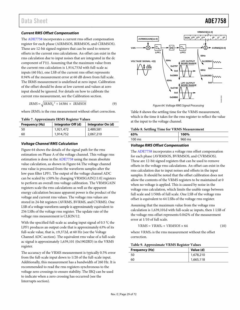
Data Sheet ADE7758
Rev. E | Page 29 of 72
Current RMS Offset Compensation
The ADE7758 incorporates a current rms offset compensation register for each phase (AIRMSOS, BIRMSOS, and CIRMSOS). These are 12-bit signed registers that can be used to remove offsets in the current rms calculations. An offset can exist in the rms calculation due to input noises that are integrated in the dc component of I2(t). Assuming that the maximum value from the current rms calculation is 1,914,753d with full-scale ac inputs (60 Hz), one LSB of the current rms offset represents 0.94% of the measurement error at 60 dB down from full scale. The IRMS measurement is undefined at zero input. Calibration of the offset should be done at low current and values at zero input should be ignored. For details on how to calibrate the current rms measurement, see the Calibration section.
IRMSOSIRMSIRMS 20 16384 (9)
where IRMS0 is the rms measurement without offset correction.
Table 7. Approximate IRMS Register Values Frequency (Hz) Integrator Off (d) Integrator On (d) 50 1,921,472 2,489,581 60 1,914,752 2,067,210
Voltage Channel RMS Calculation
Figure 64 shows the details of the signal path for the rms estimation on Phase A of the voltage channel. This voltage rms estimation is done in the ADE7758 using the mean absolute value calculation, as shown in Figure 64.The voltage channel rms value is processed from the waveform samples after the low-pass filter LPF1. The output of the voltage channel ADC can be scaled by ±50% by changing VRMSGAIN[11:0] registers to perform an overall rms voltage calibration. The VRMSGAIN registers scale the rms calculations as well as the apparent energy calculation because apparent power is the product of the voltage and current rms values. The voltage rms values are stored in 24-bit registers (AVRMS, BVRMS, and CVRMS). One LSB of a voltage waveform sample is approximately equivalent to 256 LSBs of the voltage rms register. The update rate of the voltage rms measurement is CLKIN/12.
With the specified full-scale ac analog input signal of 0.5 V, the LPF1 produces an output code that is approximately 63% of its full-scale value, that is, ±9,372d, at 60 Hz (see the Voltage Channel ADC section). The equivalent rms value of a full-scale ac signal is approximately 1,639,101 (0x1902BD) in the VRMS register.
The accuracy of the VRMS measurement is typically 0.5% error from the full-scale input down to 1/20 of the full-scale input. Additionally, this measurement has a bandwidth of 260 Hz. It is recommended to read the rms registers synchronous to the voltage zero crossings to ensure stability. The IRQ can be used to indicate when a zero crossing has occurred (see the Interrupts section).
VAN
AVRMSGAIN[11:0]
0x2748
LPF OUTPUTWORD RANGE
0x0
60Hz
0xD8B8
0x2797
LPF OUTPUTWORD RANGE
0x0
50Hz
0xD869
LPF1
VOLTAGE SIGNAL–V(t)
0.5GAIN
0x193504
50Hz
0x0
0x1902BD
60Hz
0x0
|X| AVRMS[23:0]
LPF3
SGN 216 215 214 28 27 26
VRMSOS[11:0]
++
0444
3-06
3
Figure 64. Voltage RMS Signal Processing
Table 8 shows the settling time for the VRMS measurement, which is the time it takes for the rms register to reflect the value at the input to the voltage channel.
Table 8. Settling Time for VRMS Measurement 63% 100% 100 ms 960 ms
Voltage RMS Offset Compensation
The ADE7758 incorporates a voltage rms offset compensation for each phase (AVRMSOS, BVRMSOS, and CVRMSOS). These are 12-bit signed registers that can be used to remove offsets in the voltage rms calculations. An offset can exist in the rms calculation due to input noises and offsets in the input samples. It should be noted that the offset calibration does not allow the contents of the VRMS registers to be maintained at 0 when no voltage is applied. This is caused by noise in the voltage rms calculation, which limits the usable range between full scale and 1/50th of full scale. One LSB of the voltage rms offset is equivalent to 64 LSBs of the voltage rms register.
Assuming that the maximum value from the voltage rms calculation is 1,639,101d with full-scale ac inputs, then 1 LSB of the voltage rms offset represents 0.042% of the measurement error at 1/10 of full scale.
VRMS = VRMS0 + VRMSOS × 64 (10)
where VRMS0 is the rms measurement without the offset correction.
Table 9. Approximate VRMS Register Values Frequency (Hz) Value (d) 50 1,678,210 60 1,665,118
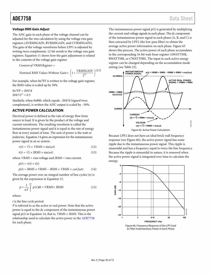
ADE7758 Data Sheet
Rev. E | Page 30 of 72
Voltage RMS Gain Adjust
The ADC gain in each phase of the voltage channel can be adjusted for the rms calculation by using the voltage rms gain registers (AVRMSGAIN, BVRMSGAIN, and CVRMSGAIN). The gain of the voltage waveforms before LPF1 is adjusted by writing twos complement, 12-bit words to the voltage rms gain registers. Equation 11 shows how the gain adjustment is related to the contents of the voltage gain register.
1221 VRMSGAINGainWithoutValuesRMSNominal
RegisterVRMSofContent(11)
For example, when 0x7FF is written to the voltage gain register, the RMS value is scaled up by 50%.
0x7FF = 2047d 2047/212 = 0.5
Similarly, when 0x800, which equals –2047d (signed twos complement), is written the ADC output is scaled by –50%.
ACTIVE POWER CALCULATION Electrical power is defined as the rate of energy flow from source to load. It is given by the product of the voltage and current waveforms. The resulting waveform is called the instantaneous power signal and it is equal to the rate of energy flow at every instant of time. The unit of power is the watt or joules/sec. Equation 14 gives an expression for the instantaneous power signal in an ac system.
v(t) = √2 × VRMS × sin(ωt) (12)
i(t) = √2 × IRMS × sin(ωt) (13)
where VRMS = rms voltage and IRMS = rms current.
p(t) = v(t) × i(t)
p(t) = IRMS × VRMS − IRMS × VRMS × cos(2ωt) (14)
The average power over an integral number of line cycles (n) is given by the expression in Equation 15.
IRMSVRMSdttpnT
pnT
0
1 (15)
where:
t is the line cycle period. P is referred to as the active or real power. Note that the active power is equal to the dc component of the instantaneous power signal p(t) in Equation 14, that is, VRMS × IRMS. This is the relationship used to calculate the active power in the ADE7758 for each phase.
The instantaneous power signal p(t) is generated by multiplying the current and voltage signals in each phase. The dc component of the instantaneous power signal in each phase (A, B, and C) is then extracted by LPF2 (the low-pass filter) to obtain the average active power information on each phase. Figure 65 shows this process. The active power of each phase accumulates in the corresponding 16-bit watt-hour register (AWATTHR, BWATTHR, or CWATTHR). The input to each active energy register can be changed depending on the accumulation mode setting (see Table 22).
INSTANTANEOUSPOWER SIGNAL p(t) = VRMS × IRMS – VRMS × IRMS × cos(2ωt)
ACTIVE REAL POWERSIGNAL = VRMS × IRMS
0x19999A
VRMS × IRMS0xCCCCD
0x00000
CURRENTi(t) = 2 × IRMS × sin(ωt)
VOLTAGEv(t) = 2 × VRMS × sin(ωt) 04
443-
064
Figure 65. Active Power Calculation
Because LPF2 does not have an ideal brick wall frequency response (see Figure 66), the active power signal has some ripple due to the instantaneous power signal. This ripple is sinusoidal and has a frequency equal to twice the line frequency. Because the ripple is sinusoidal in nature, it is removed when the active power signal is integrated over time to calculate the energy.
0
–4
–8
–12
GA
IN (d
B)
–16
–20
–241 3 108
FREQUENCY (Hz)
30 100
0444
3-06
5
Figure 66. Frequency Response of the LPF Used
to Filter Instantaneous Power in Each Phase

Data Sheet ADE7758
Rev. E | Page 31 of 72
Active Power Gain Calibration
Note that the average active power result from the LPF output in each phase can be scaled by ±50% by writing to the phase’s watt gain register (AWG, BWG, or CWG). The watt gain registers are twos complement, signed registers and have a resolution of 0.024%/LSB. Equation 16 describes mathematically the function of the watt gain registers.
⎟⎠
⎞⎜⎝
⎛ +×
=
12212
gisterReGainWattOutputLPF
DataPowerAverage
(16)
The REVPAP bit (Bit 17) in the interrupt status register is set if the average power from any one of the phases changes sign. The phases monitored are selected by TERMSEL bits in the COMPMODE register (see Table 21). The TERMSEL bits are also used to select which phases are included in the APCF and VARCF pulse outputs. If the REVPAP bit is set in the mask register, the IRQ logic output goes active low (see the section). Note that this bit is set whenever there are sign changes, that is, the REVPAP bit is set for both a positive-to-negative change and a negative-to-positive change of the sign bit. The response time of this bit is approximately 176 ms for a full-scale signal, which has an average value of 0xCCCCD at the low pass filter output. For smaller inputs, the time is longer.
Interrupts
The output is scaled by −50% by writing 0x800 to the watt gain registers and increased by +50% by writing 0x7FF to them. These registers can be used to calibrate the active power (or energy) calculation in the ADE7758 for each phase.
CLKINValueAveragemsTimesponseRe 4252601 ×
⎥⎥⎦
⎤
⎢⎢⎣
⎡+≅ (17)
Active Power Offset Calibration The APCFNUM [15:13] indicate reverse power on each of the individual phases. Bit 15 is set if the sign of the power on Phase A is negative, Bit 14 for Phase B, and Bit 13 for Phase C.
The ADE7758 also incorporates a watt offset register on each phase (AWATTOS, BWATTOS, and CWATTOS). These are signed twos complement, 12-bit registers that are used to remove offsets in the active power calculations. An offset can exist in the power calculation due to crosstalk between channels on the PCB or in the chip itself. The offset calibration allows the contents of the active power register to be maintained at 0 when no power is being consumed. One LSB in the active power offset register is equivalent to 1/16 LSB in the active power multiplier output. At full-scale input, if the output from the multiplier is 0xCCCCD (838,861d), then 1 LSB in the LPF2 output is equivalent to 0.0075% of measurement error at 60 dB down from full scale on the current channel. At −60 dB down on full scale (the input signal level is 1/1000 of full-scale signal inputs), the average word value from LPF2 is 838.861 (838,861/1000). One LSB is equivalent to 1/838.861/16 × 100% = 0.0075% of the measured value. The active power offset register has a correction resolution equal to 0.0075% at −60 dB.
No-Load Threshold
The ADE7758 has an internal no-load threshold on each phase. The no-load threshold can be activated by setting the NOLOAD bit (Bit 7) of the COMPMODE register. If the active power falls below 0.005% of full-scale input, the energy is not accumulated in that phase. As stated, the average multiplier output with full-scale input is 0xCCCCD. Therefore, if the average multiplier output falls below 0x2A, the power is not accumulated to avoid creep in the meter. The no-load threshold is implemented only on the active energy accumulation. The reactive and apparent energies do not have the no-load threshold option.
Active Energy Calculation
As previously stated, power is defined as the rate of energy flow. This relationship can be expressed mathematically as
dtdEnergyPower = (18) Sign of Active Power Calculation
Note that the average active power is a signed calculation. If the phase difference between the current and voltage waveform is more than 90°, the average power becomes negative. Negative power indicates that energy is being placed back on the grid. The ADE7758 has a sign detection circuitry for active power calculation.
Conversely, Energy is given as the integral of power.
( )dtp∫= tEnergy (19)
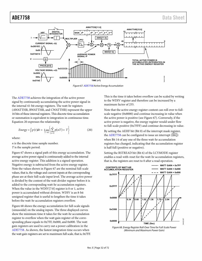
ADE7758 Data Sheet
Rev. E | Page 32 of 72
AWG[11:0]
WDIV[7:0]
DIGITALINTEGRATOR
MULTIPLIERI
V
HPF
CURRENT SIGNAL–i(t)0x2851EC
0x00
0xD7AE14
VOLTAGE SIGNAL–v(t)0x2852
000x
0xD7AE
+ + +
+
LPF2
%
SIGN 26 20 2–1 2–2 2–3 2–4
AWATTOS[11:0]AWATTHR[15:0]
15 0
40 0
TOTAL ACTIVE POWER ISACCUMULATED (INTEGRATED) INTHE ACTIVE ENERGY REGISTER
TIME (nT)
T
AVERAGE POWERSIGNAL–P
0xCCCCD
0x00000
PHCAL[6:0]
Φ
0444
3-06
6
Figure 67. ADE7758 Active Energy Accumulation
The ADE7758 achieves the integration of the active power signal by continuously accumulating the active power signal in the internal 41-bit energy registers. The watt-hr registers (AWATTHR, BWATTHR, and CWATTHR) represent the upper 16 bits of these internal registers. This discrete time accumulation or summation is equivalent to integration in continuous time. Equation 20 expresses the relationship.
( ) ( )⎭⎬⎫
⎩⎨⎧ ×== ∑∫
∞
=→ 00TLim
nTnTpdttpEnergy (20)
where:
n is the discrete time sample number. T is the sample period.
Figure 67 shows a signal path of this energy accumulation. The average active power signal is continuously added to the internal active energy register. This addition is a signed operation. Negative energy is subtracted from the active energy register. Note the values shown in Figure 67 are the nominal full-scale values, that is, the voltage and current inputs at the corresponding phase are at their full-scale input level. The average active power is divided by the content of the watt divider register before it is added to the corresponding watt-hr accumulation registers. When the value in the WDIV[7:0] register is 0 or 1, active power is accumulated without division. WDIV is an 8-bit unsigned register that is useful to lengthen the time it takes before the watt-hr accumulation registers overflow.
Figure 68 shows the energy accumulation for full-scale signals (sinusoidal) on the analog inputs. The three displayed curves show the minimum time it takes for the watt-hr accumulation register to overflow when the watt gain register of the corre-sponding phase equals to 0x7FF, 0x000, and 0x800. The watt gain registers are used to carry out a power calibration in the ADE7758. As shown, the fastest integration time occurs when the watt gain registers are set to maximum full scale, that is, 0x7FF.
This is the time it takes before overflow can be scaled by writing to the WDIV register and therefore can be increased by a maximum factor of 255.
Note that the active energy register content can roll over to full-scale negative (0x8000) and continue increasing in value when the active power is positive (see Figure 67). Conversely, if the active power is negative, the energy register would under flow to full-scale positive (0x7FFF) and continue decreasing in value.
By setting the AEHF bit (Bit 0) of the interrupt mask register, the ADE7758 can be configured to issue an interrupt (IRQ) when Bit 14 of any one of the three watt-hr accumulation registers has changed, indicating that the accumulation register is half full (positive or negative).
Setting the RSTREAD bit (Bit 6) of the LCYMODE register enables a read-with-reset for the watt-hr accumulation registers, that is, the registers are reset to 0 after a read operation.
CONTENTS OF WATT-HRACCUMULATION REGISTER
0x7FFF
0x3FFF
0x0000
0xC000
0x8000TIME (Sec)
0.34 0.68 1.02 1.36 1.70 2.04
WATT GAIN = 0x7FFWATT GAIN = 0x000WATT GAIN = 0x800
0444
3-06
7
Figure 68. Energy Register Roll-Over Time for Full-Scale Power
(Minimum and Maximum Power Gain)

Data Sheet ADE7758
Rev. E | Page 33 of 72
Integration Time Under Steady Load
The discrete time sample period (T) for the accumulation register is 0.4 μs (4/CLKIN). With full-scale sinusoidal signals on the analog inputs and the watt gain registers set to 0x000, the average word value from each LPF2 is 0xCCCCD (see Figure 65 and Figure 67). The maximum value that can be stored in the watt-hr accumulation register before it overflows is 215 − 1 or 0x7FFF. Because the average word value is added to the internal register, which can store 240 − 1 or 0xFF, FFFF, FFFF before it overflows, the integration time under these conditions with WDIV = 0 is calculated as
sec0.524μs0.40xCCCCD
FFFFFFFF,0xFF,=×=Time (21)
When WDIV is set to a value different from 0, the time before overflow is scaled accordingly as shown in Equation 22.
Time = Time (WDIV = 0) × WDIV[7:0] (22)
Energy Accumulation Mode
The active power accumulated in each watt-hr accumulation register (AWATTHR, BWATTHR, or CWATTHR) depends on the configuration of the CONSEL bits in the COMPMODE register (Bit 0 and Bit 1). The different configurations are described in Table 10.
Table 10. Inputs to Watt-Hr Accumulation Registers CONSEL[1, 0] AWATTHR BWATTHR CWATTHR 00 VA × IA VB × IB VC × IC 01 VA × (IA – IB) 0 VC × (IC – IB) 10 VA × (IA – IB) 0 VC × IC 11 Reserved Reserved Reserved
Depending on the poly phase meter service, the appropriate formula should be chosen to calculate the active energy. The American ANSI C12.10 Standard defines the different configurations of the meter.
Table 11 describes which mode should be chosen in these different configurations.
Table 11. Meter Form Configuration ANSI Meter Form CONSEL (d) TERMSEL (d)
5S/13S 3-Wire Delta 0 3, 5, or 6 6S/14S 4-Wire Wye 1 7 8S/15S 4-Wire Delta 2 7 9S/16S 4-Wire Wye 0 7
Active Power Frequency Output
Pin 1 (APCF) of the ADE7758 provides frequency output for the total active power. After initial calibration during manufac-turing, the manufacturer or end customer often verifies the energy meter calibration. One convenient way to verify the meter calibration is for the manufacturer to provide an output frequency that is proportional to the energy or active power under steady load conditions. This output frequency can provide a
simple, single-wire, optically isolated interface to external calibration equipment. Figure 69 illustrates the energy-to-frequency conversion in the ADE7758.
INPUT TO BWATTHRREGISTER
INPUT TO AWATTHRREGISTER
INPUT TO CWATTHRREGISTER
DFC APCF
APCFNUM[11:0]
APCFDEN[11:0]
÷+
++
÷4
0444
3-06
8
Figure 69. Active Power Frequency Output
A digital-to-frequency converter (DFC) is used to generate the APCF pulse output from the total active power. The TERMSEL bits (Bit 2 to Bit 4) of the COMPMODE register can be used to select which phases to include in the total power calculation. Setting Bit 2, Bit 3, and Bit 4 includes the input to the AWATTHR, BWATTHR, and CWATTHR registers in the total active power calculation. The total active power is signed addition. However, setting the ABS bit (Bit 5) in the COMPMODE register enables the absolute-only mode; that is, only the absolute value of the active power is considered.
The output from the DFC is divided down by a pair of frequency division registers before being sent to the APCF pulse output. Namely, APCFDEN/APCFNUM pulses are needed at the DFC output before the APCF pin outputs a pulse. Under steady load conditions, the output frequency is directly proportional to the total active power. The pulse width of APCF is 64/CLKIN if APCFNUM and APCFDEN are both equal. If APCFDEN is greater than APCFNUM, the pulse width depends on APCFDEN. The pulse width in this case is T × (APCFDEN/2), where T is the period of the APCF pulse and APCFDEN/2 is rounded to the nearest whole number. An exception to this is when the period is greater than 180 ms. In this case, the pulse width is fixed at 90 ms.
The maximum output frequency (APCFNUM = 0x00 and APCFDEN = 0x00) with full-scale ac signals on one phase is approximately 16 kHz.
The ADE7758 incorporates two registers to set the frequency of APCF (APCFNUM[11:0] and APCFDEN[11:0]). These are unsigned 12-bit registers that can be used to adjust the frequency of APCF by 1/212 to 1 with a step of 1/212. For example, if the output frequency is 1.562 kHz while the contents of APCFDEN are 0 (0x000), then the output frequency can be set to 6.103 Hz by writing 0xFF to the APCFDEN register.
If 0 were written to any of the frequency division registers, the divider would use 1 in the frequency division. In addition, the ratio APCFNUM/APCFDEN should be set not greater than 1 to ensure proper operation. In other words, the APCF output frequency cannot be higher than the frequency on the DFC output.
The output frequency has a slight ripple at a frequency equal to 2× the line frequency. This is due to imperfect filtering of the instantaneous power signal to generate the active power signal
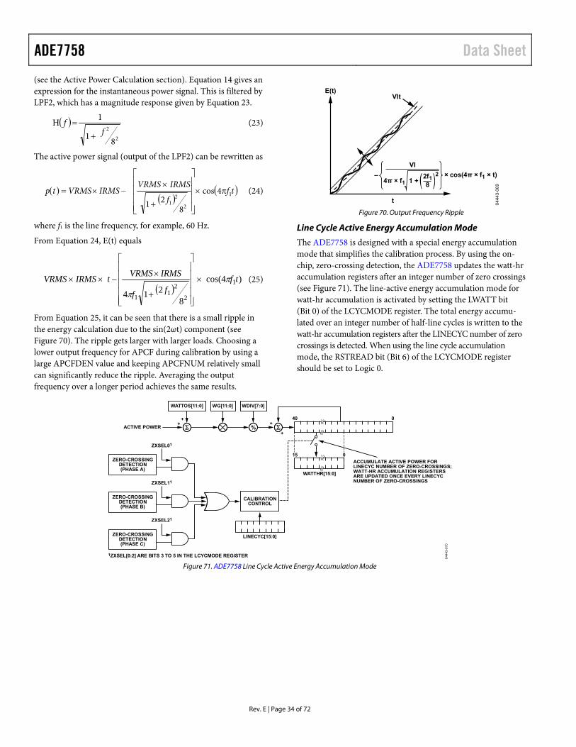
ADE7758 Data Sheet
Rev. E | Page 34 of 72
(see the Active Power Calculation section). Equation 14 gives an expression for the instantaneous power signal. This is filtered by LPF2, which has a magnitude response given by Equation 23.
( )2
2
81
1Hf
f+
= (23)
–
E(t)
t
Vlt
VI× cos(4π × f1 × t)
4π × f1 1 +22f1
8
0444
3-06
9
The active power signal (output of the LPF2) can be rewritten as
( )( )
( tff
IRMSVRMSIRMSVRMStp 1
2
21
4cos
821
π×
⎥⎥⎥⎥
⎦
⎤
⎢⎢⎢⎢
⎣
⎡
+
×−×= ) (24)
Figure 70. Output Frequency Ripple
where f1 is the line frequency, for example, 60 Hz. Line Cycle Active Energy Accumulation Mode From Equation 24, E(t) equals The ADE7758 is designed with a special energy accumulation
mode that simplifies the calibration process. By using the on-chip, zero-crossing detection, the ADE7758 updates the watt-hr accumulation registers after an integer number of zero crossings (see Figure 71). The line-active energy accumulation mode for watt-hr accumulation is activated by setting the LWATT bit (Bit 0) of the LCYCMODE register. The total energy accumu-lated over an integer number of half-line cycles is written to the watt-hr accumulation registers after the LINECYC number of zero crossings is detected. When using the line cycle accumulation mode, the RSTREAD bit (Bit 6) of the LCYCMODE register should be set to Logic 0.
( ))4cos(
8214
– 1
2
21
1
tfff
IRMSVRMStIRMSVRMS π
π
×
⎥⎥⎥⎥⎥
⎦
⎤
⎢⎢⎢⎢⎢
⎣
⎡
+
××× (25)
From Equation 25, it can be seen that there is a small ripple in the energy calculation due to the sin(2ωt) component (see Figure 70). The ripple gets larger with larger loads. Choosing a lower output frequency for APCF during calibration by using a large APCFDEN value and keeping APCFNUM relatively small can significantly reduce the ripple. Averaging the output frequency over a longer period achieves the same results.
ZXSEL01
ZERO-CROSSINGDETECTION(PHASE A)
ZXSEL11
ZERO-CROSSINGDETECTION(PHASE B)
ZXSEL21
ZERO-CROSSINGDETECTION(PHASE C)
1ZXSEL[0:2] ARE BITS 3 TO 5 IN THE LCYCMODE REGISTER
CALIBRATIONCONTROL
LINECYC[15:0]
WATTOS[11:0] WG[11:0] WDIV[7:0]
++
%+
+
WATTHR[15:0]
ACCUMULATE ACTIVE POWER FORLINECYC NUMBER OF ZERO-CROSSINGS;WATT-HR ACCUMULATION REGISTERSARE UPDATED ONCE EVERY LINECYCNUMBER OF ZERO-CROSSINGS
ACTIVE POWER
15 0
40 0
0444
3-07
0
Figure 71. ADE7758 Line Cycle Active Energy Accumulation Mode

Data Sheet ADE7758
Rev. E | Page 35 of 72
Phase A, Phase B, and Phase C zero crossings are, respectively, included when counting the number of half-line cycles by setting ZXSEL[0:2] bits (Bit 3 to Bit 5) in the LCYCMODE register. Any combination of the zero crossings from all three phases can be used for counting the zero crossing. Only one phase should be selected at a time for inclusion in the zero crossings count during calibration (see the Calibration section).
The number of zero crossings is specified by the LINECYC register. LINECYC is an unsigned 16-bit register. The ADE7758 can accumulate active power for up to 65535 combined zero crossings. Note that the internal zero-crossing counter is always active. By setting the LWATT bit, the first energy accumulation result is, therefore, incorrect. Writing to the LINECYC register when the LWATT bit is set resets the zero-crossing counter, thus ensuring that the first energy accumulation result is accurate.
At the end of an energy calibration cycle, the LENERGY bit (Bit 12) in the STATUS register is set. If the corresponding mask bit in the interrupt mask register is enabled, the IRQ output also goes active low; thus, the IRQ can also be used to signal the end of a calibration.
Because active power is integrated on an integer number of half-line cycles in this mode, the sinusoidal component is reduced to 0, eliminating any ripple in the energy calculation. Therefore, total energy accumulated using the line-cycle accumulation mode is
E(t) = VRMS × IRMS × t (26)
where t is the accumulation time.
Note that line cycle active energy accumulation uses the same signal path as the active energy accumulation. The LSB size of these two methods is equivalent. Using the line cycle accumula-tion to calculate the kWh/LSB constant results in a value that can be applied to the WATTHR registers when the line accumulation mode is not selected (see the Calibration section).
REACTIVE POWER CALCULATION A load that contains a reactive element (inductor or capacitor) produces a phase difference between the applied ac voltage and the resulting current. The power associated with reactive elements is called reactive power, and its unit is VAR. Reactive power is defined as the product of the voltage and current waveforms when one of these signals is phase shifted by 90°.
Equation 30 gives an expression for the instantaneous reactive power signal in an ac system when the phase of the current channel is shifted by +90°.
( ) ( θ= –sin2 ωtVtv ) (27)
( ) ( )
( ) ⎟⎠⎞
⎜⎝⎛ π
+=′
=
2sin2i
sin2
ωtIt
ωtIti (28)
where:
v = rms voltage. i = rms current. θ = total phase shift caused by the reactive elements in the load.
Then the instantaneous reactive power q(t) can be expressed as
( ) ( ) ( )
( ) ⎟⎠⎞
⎜⎝⎛ π
θ⎟⎠⎞
⎜⎝⎛ π
θ=
′×=
2––2cos–
2––cos ωtVIVItq
titvtq (29)
where ( )ti′ is the current waveform phase shifted by 90°. Note that q(t) can be rewritten as
( ) ( ) ( θ)+θ= –2sinsin ωtVIVItq (30)
The average reactive power over an integral number of line cycles (n) is given by the expression in Equation 31.
( ) ( )∫ ××==nT
0
θsindtnT1 IVtqQ (31)
where:
T is the period of the line cycle. Q is referred to as the average reactive power. The instantaneous reactive power signal q(t) is generated by multiplying the voltage signals and the 90° phase-shifted current in each phase.
The dc component of the instantaneous reactive power signal in each phase (A, B, and C) is then extracted by a low-pass filter to obtain the average reactive power information on each phase. This process is illustrated in Figure 72. The reactive power of each phase is accumulated in the corresponding 16-bit VAR-hour register (AVARHR, BVARHR, or CVARHR). The input to each reactive energy register can be changed depending on the accumulation mode setting (see Table 21).
The frequency response of the LPF in the reactive power signal path is identical to that of the LPF2 used in the average active power calculation (see Figure 66).
VRMS × IRMS × sin(φ)
θ
0x00000
CURRENTi(t) = 2 × IRMS × sin(ωt)
VOLTAGEv(t) = 2 × VRMS × sin(ωt – θ)
INSTANTANEOUSREACTIVE POWER SIGNALq(t) = VRMS × IRMS × sin(φ) + VRMS × IRMS × sin(2ωt + θ)
AVERAGE REACTIVE POWER SIGNAL =VRMS × IRMS × sin(θ)
0444
3-07
1
Figure 72. Reactive Power Calculation
The low-pass filter is nonideal, so the reactive power signal has some ripple. This ripple is sinusoidal and has a frequency equal to 2× the line frequency. Because the ripple is sinusoidal in nature, it is removed when the reactive power signal is integrated over time to calculate the reactive energy.
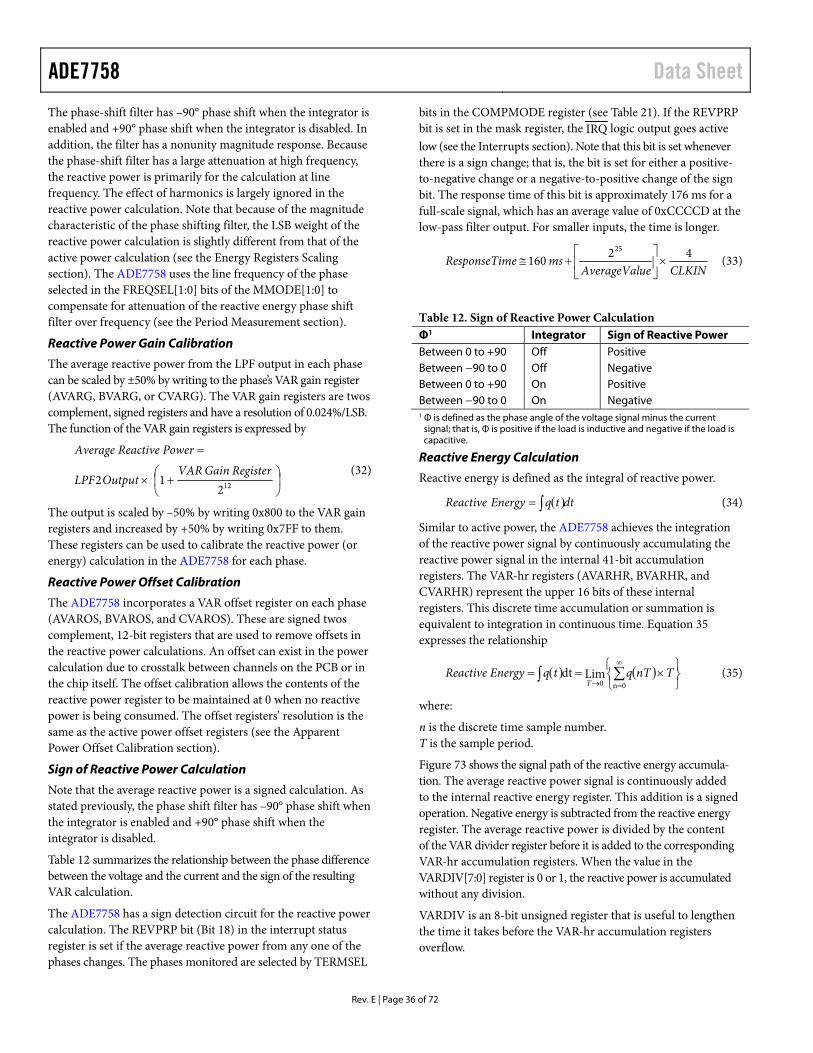
ADE7758 Data Sheet
Rev. E | Page 36 of 72
The phase-shift filter has –90° phase shift when the integrator is enabled and +90° phase shift when the integrator is disabled. In addition, the filter has a nonunity magnitude response. Because the phase-shift filter has a large attenuation at high frequency, the reactive power is primarily for the calculation at line frequency. The effect of harmonics is largely ignored in the reactive power calculation. Note that because of the magnitude characteristic of the phase shifting filter, the LSB weight of the reactive power calculation is slightly different from that of the active power calculation (see the Energy Registers Scaling section). The ADE7758 uses the line frequency of the phase selected in the FREQSEL[1:0] bits of the MMODE[1:0] to compensate for attenuation of the reactive energy phase shift filter over frequency (see the Period Measurement section).
Reactive Power Gain Calibration
The average reactive power from the LPF output in each phase can be scaled by ±50% by writing to the phase’s VAR gain register (AVARG, BVARG, or CVARG). The VAR gain registers are twos complement, signed registers and have a resolution of 0.024%/LSB. The function of the VAR gain registers is expressed by
⎟⎠
⎞⎜⎝
⎛ +×
=
12212
gisterReGainVAROutputLPF
PowerReactiveAverage
(32)
The output is scaled by –50% by writing 0x800 to the VAR gain registers and increased by +50% by writing 0x7FF to them. These registers can be used to calibrate the reactive power (or energy) calculation in the ADE7758 for each phase.
Reactive Power Offset Calibration
The ADE7758 incorporates a VAR offset register on each phase (AVAROS, BVAROS, and CVAROS). These are signed twos complement, 12-bit registers that are used to remove offsets in the reactive power calculations. An offset can exist in the power calculation due to crosstalk between channels on the PCB or in the chip itself. The offset calibration allows the contents of the reactive power register to be maintained at 0 when no reactive power is being consumed. The offset registers’ resolution is the same as the active power offset registers (see the Apparent Power Offset Calibration section).
Sign of Reactive Power Calculation
Note that the average reactive power is a signed calculation. As stated previously, the phase shift filter has –90° phase shift when the integrator is enabled and +90° phase shift when the integrator is disabled.
Table 12 summarizes the relationship between the phase difference between the voltage and the current and the sign of the resulting VAR calculation.
The ADE7758 has a sign detection circuit for the reactive power calculation. The REVPRP bit (Bit 18) in the interrupt status register is set if the average reactive power from any one of the phases changes. The phases monitored are selected by TERMSEL
bits in the COMPMODE register (see Table 21). If the REVPRP bit is set in the mask register, the IRQ logic output goes active low (see the section). Note that this bit is set whenever there is a sign change; that is, the bit is set for either a positive-to-negative change or a negative-to-positive change of the sign bit. The response time of this bit is approximately 176 ms for a full-scale signal, which has an average value of 0xCCCCD at the low-pass filter output. For smaller inputs, the time is longer.
Interrupts
CLKINueAverageValmssponseTimeRe 42601
25
×⎥⎦
⎤⎢⎣
⎡+≅ (33)
Table 12. Sign of Reactive Power Calculation Φ1 Integrator Sign of Reactive Power Between 0 to +90 Off Positive Between −90 to 0 Off Negative Between 0 to +90 On Positive Between −90 to 0 On Negative 1 Φ is defined as the phase angle of the voltage signal minus the current
signal; that is, Φ is positive if the load is inductive and negative if the load is capacitive.
Reactive Energy Calculation
Reactive energy is defined as the integral of reactive power.
( )dttqEnergyReactive ∫= (34)
Similar to active power, the ADE7758 achieves the integration of the reactive power signal by continuously accumulating the reactive power signal in the internal 41-bit accumulation registers. The VAR-hr registers (AVARHR, BVARHR, and CVARHR) represent the upper 16 bits of these internal registers. This discrete time accumulation or summation is equivalent to integration in continuous time. Equation 35 expresses the relationship
( ) ( )⎭⎬⎫
⎩⎨⎧ ×== ∑∫
∞
=→ 0n0Limdt TnTqtqEnergyReactiveT
(35)
where:
n is the discrete time sample number. T is the sample period.
Figure 73 shows the signal path of the reactive energy accumula-tion. The average reactive power signal is continuously added to the internal reactive energy register. This addition is a signed operation. Negative energy is subtracted from the reactive energy register. The average reactive power is divided by the content of the VAR divider register before it is added to the corresponding VAR-hr accumulation registers. When the value in the VARDIV[7:0] register is 0 or 1, the reactive power is accumulated without any division.
VARDIV is an 8-bit unsigned register that is useful to lengthen the time it takes before the VAR-hr accumulation registers overflow.

Data Sheet ADE7758
Rev. E | Page 37 of 72
Similar to reactive power, the fastest integration time occurs when the VAR gain registers are set to maximum full scale, that is, 0x7FF. The time it takes before overflow can be scaled by writing to the VARDIV register; and, therefore, it can be increased by a maximum factor of 255.
By setting the REHF bit (Bit 1) of the interrupt mask register, the ADE7758 can be configured to issue an interrupt (IRQ) when Bit 14 of any one of the three VAR-hr accumulation registers has changed, indicating that the accumulation register is half full (positive or negative).
When overflow occurs, the VAR-hr accumulation registers content can rollover to full-scale negative (0x8000) and continue increasing in value when the reactive power is positive. Con-versely, if the reactive power is negative, the VAR-hr accumulation registers content can roll over to full-scale positive (0x7FFF) and continue decreasing in value.
Setting the RSTREAD bit (Bit 6) of the LCYMODE register enables a read-with-reset for the VAR-hr accumulation registers; that is, the registers are reset to 0 after a read operation.
VARG[11:0]
VARDIV[7:0]
90° PHASESHIFTING FILTER
MULTIPLIERI
V
HPF
CURRENT SIGNAL–i(t)0x2851EC
0x00
0xD7AE14
VOLTAGE SIGNAL–v(t)0x2852
0x00
0xD7AE
+ + +
+
LPF2
%
SIGN 26 20 2–1 2–2 2–3 2–4
VAROS[11:0]VARHR[15:0]
15 0
40 0
TOTAL REACTIVE POWER ISACCUMULATED (INTEGRATED) INTHE VAR-HR ACCUMULATION REGISTERS
π2
PHCAL[6:0]
Φ
0444
3-07
2
Figure 73. ADE7758 Reactive Energy Accumulation
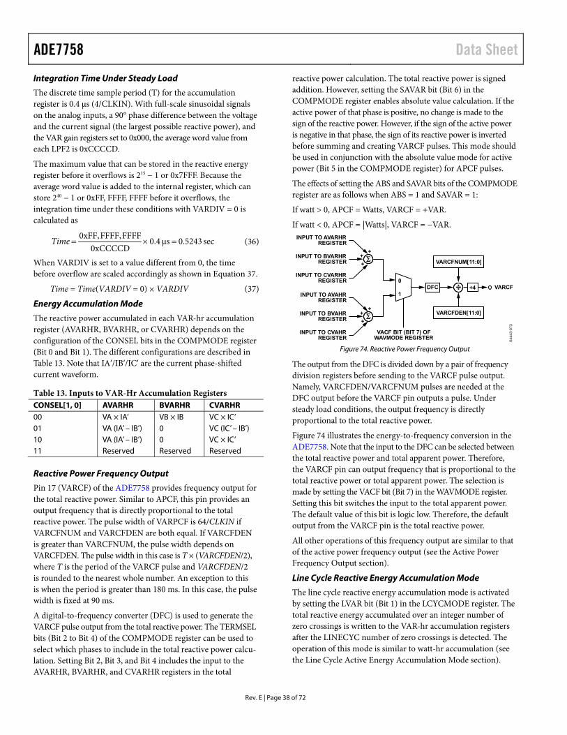
ADE7758 Data Sheet
Rev. E | Page 38 of 72
Integration Time Under Steady Load
The discrete time sample period (T) for the accumulation register is 0.4 μs (4/CLKIN). With full-scale sinusoidal signals on the analog inputs, a 90° phase difference between the voltage and the current signal (the largest possible reactive power), and the VAR gain registers set to 0x000, the average word value from each LPF2 is 0xCCCCD.
The maximum value that can be stored in the reactive energy register before it overflows is 215 − 1 or 0x7FFF. Because the average word value is added to the internal register, which can store 240 − 1 or 0xFF, FFFF, FFFF before it overflows, the integration time under these conditions with VARDIV = 0 is calculated as
sec0.5243μs0.40xCCCCD
FFFFFFFF,0xFF,=×=Time (36)
When VARDIV is set to a value different from 0, the time before overflow are scaled accordingly as shown in Equation 37.
Time = Time(VARDIV = 0) × VARDIV (37)
Energy Accumulation Mode
The reactive power accumulated in each VAR-hr accumulation register (AVARHR, BVARHR, or CVARHR) depends on the configuration of the CONSEL bits in the COMPMODE register (Bit 0 and Bit 1). The different configurations are described in Table 13. Note that IA’/IB’/IC’ are the current phase-shifted current waveform.
Table 13. Inputs to VAR-Hr Accumulation Registers CONSEL[1, 0] AVARHR BVARHR CVARHR 00 VA × IA’ VB × IB VC × IC’ 01 VA (IA’ – IB’) 0 VC (IC’ – IB’) 10 VA (IA’ – IB’) 0 VC × IC’ 11 Reserved Reserved Reserved
Reactive Power Frequency Output
Pin 17 (VARCF) of the ADE7758 provides frequency output for the total reactive power. Similar to APCF, this pin provides an output frequency that is directly proportional to the total reactive power. The pulse width of VARPCF is 64/CLKIN if VARCFNUM and VARCFDEN are both equal. If VARCFDEN is greater than VARCFNUM, the pulse width depends on VARCFDEN. The pulse width in this case is T × (VARCFDEN/2), where T is the period of the VARCF pulse and VARCFDEN/2 is rounded to the nearest whole number. An exception to this is when the period is greater than 180 ms. In this case, the pulse width is fixed at 90 ms.
A digital-to-frequency converter (DFC) is used to generate the VARCF pulse output from the total reactive power. The TERMSEL bits (Bit 2 to Bit 4) of the COMPMODE register can be used to select which phases to include in the total reactive power calcu-lation. Setting Bit 2, Bit 3, and Bit 4 includes the input to the AVARHR, BVARHR, and CVARHR registers in the total
reactive power calculation. The total reactive power is signed addition. However, setting the SAVAR bit (Bit 6) in the COMPMODE register enables absolute value calculation. If the active power of that phase is positive, no change is made to the sign of the reactive power. However, if the sign of the active power is negative in that phase, the sign of its reactive power is inverted before summing and creating VARCF pulses. This mode should be used in conjunction with the absolute value mode for active power (Bit 5 in the COMPMODE register) for APCF pulses.
The effects of setting the ABS and SAVAR bits of the COMPMODE register are as follows when ABS = 1 and SAVAR = 1:
If watt > 0, APCF = Watts, VARCF = +VAR.
If watt < 0, APCF = |Watts|, VARCF = −VAR.
INPUT TO BVARHRREGISTER
INPUT TO AVARHRREGISTER
INPUT TO CVARHRREGISTER
+++
INPUT TO BVAHRREGISTER
INPUT TO AVAHRREGISTER
INPUT TO CVAHRREGISTER
+++
0
1VARCF
VARCFNUM[11:0]
VARCFDEN[11:0]
÷DFC
VACF BIT (BIT 7) OFWAVMODE REGISTER
÷4
0444
3-07
3
Figure 74. Reactive Power Frequency Output
The output from the DFC is divided down by a pair of frequency division registers before sending to the VARCF pulse output. Namely, VARCFDEN/VARCFNUM pulses are needed at the DFC output before the VARCF pin outputs a pulse. Under steady load conditions, the output frequency is directly proportional to the total reactive power.
Figure 74 illustrates the energy-to-frequency conversion in the ADE7758. Note that the input to the DFC can be selected between the total reactive power and total apparent power. Therefore, the VARCF pin can output frequency that is proportional to the total reactive power or total apparent power. The selection is made by setting the VACF bit (Bit 7) in the WAVMODE register. Setting this bit switches the input to the total apparent power. The default value of this bit is logic low. Therefore, the default output from the VARCF pin is the total reactive power.
All other operations of this frequency output are similar to that of the active power frequency output (see the Active Power Frequency Output section).
Line Cycle Reactive Energy Accumulation Mode
The line cycle reactive energy accumulation mode is activated by setting the LVAR bit (Bit 1) in the LCYCMODE register. The total reactive energy accumulated over an integer number of zero crossings is written to the VAR-hr accumulation registers after the LINECYC number of zero crossings is detected. The operation of this mode is similar to watt-hr accumulation (see the Line Cycle Active Energy Accumulation Mode section).

Data Sheet ADE7758
Rev. E | Page 39 of 72
When using the line cycle accumulation mode, the RSTREAD bit (Bit 6) of the LCYCMODE register should be set to Logic 0.
APPARENT POWER CALCULATION Apparent power is defined as the amplitude of the vector sum of the active and reactive powers. Figure 75 shows what is typically referred to as the power triangle.
REA
CTI
VE P
OW
ER
ACTIVE POWER
APPARENTPOWER
θ
0444
3-07
4
Figure 75. Power Triangle
There are two ways to calculate apparent power: the arithmetical approach or the vectorial method. The arithmetical approach uses the product of the voltage rms value and current rms value to calculate apparent power. Equation 38 describes the arithmetical approach mathematically.
S = VRMS × IRMS (38)
where S is the apparent power, and VRMS and IRMS are the rms voltage and current, respectively.
The vectorial method uses the square root of the sum of the active and reactive power, after the two are individually squared. Equation 39 shows the calculation used in the vectorial approach.
22 QPS += (39)
where:
S is the apparent power. P is the active power. Q is the reactive power.
For a pure sinusoidal system, the two approaches should yield the same result. The apparent energy calculation in the ADE7758 uses the arithmetical approach. However, the line cycle energy accumulation mode in the ADE7758 enables energy accumula-tion between active and reactive energies over a synchronous period, thus the vectorial method can be easily implemented in the external MCU (see the Line Cycle Active Energy Accumulation Mode section).
Note that apparent power is always positive regardless of the direction of the active or reactive energy flows. The rms value of the current and voltage in each phase is multiplied to produce the apparent power of the corresponding phase.
The output from the multiplier is then low-pass filtered to obtain the average apparent power. The frequency response of the LPF in the apparent power signal path is identical to that of the LPF2 used in the average active power calculation (see Figure 66).
Apparent Power Gain Calibration
Note that the average active power result from the LPF output in each phase can be scaled by ±50% by writing to the phase’s VAGAIN register (AVAG, BVAG, or CVAG). The VAGAIN registers are twos complement, signed registers and have a resolution of 0.024%/LSB. The function of the VAGAIN registers is expressed mathematically as
⎟⎠
⎞⎜⎝
⎛ +×
=
12212
RegisterVAGAINOutputLPF
PowerApparentAverage
(40)
The output is scaled by –50% by writing 0x800 to the VAR gain registers and increased by +50% by writing 0x7FF to them. These registers can be used to calibrate the apparent power (or energy) calculation in the ADE7758 for each phase.
Apparent Power Offset Calibration
Each rms measurement includes an offset compensation register to calibrate and eliminate the dc component in the rms value (see the Current RMS Calculation section and the Voltage Channel RMS Calculation section). The voltage and current rms values are then multiplied together in the apparent power signal processing. As no additional offsets are created in the multiplication of the rms values, there is no specific offset compensation in the apparent power signal processing. The offset compensation of the apparent power measurement in each phase should be done by calibrating each individual rms measurement (see the Calibration section).

ADE7758 Data Sheet
Rev. E | Page 40 of 72
Apparent Energy Calculation
Apparent energy is defined as the integral of apparent power.
Apparent Energy = ∫ S(t)dt (41)
Similar to active or reactive power accumulation, the fastest integration time occurs when the VAGAIN registers are set to maximum full scale, that is, 0x7FF. When overflow occurs, the content of the VA-hr accumulation registers can roll over to 0 and continue increasing in value. Similar to active and reactive energy, the ADE7758 achieves the
integration of the apparent power signal by continuously accumulating the apparent power signal in the internal 41-bit, unsigned accumulation registers. The VA-hr registers (AVAHR, BVAHR, and CVAHR) represent the upper 16 bits of these internal registers. This discrete time accumulation or summation is equivalent to integration in continuous time. Equation 42 expresses the relationship
By setting the VAEHF bit (Bit 2) of the mask register, the ADE7758 can be configured to issue an interrupt (IRQ) when the MSB of any one of the three VA-hr accumulation registers has changed, indicating that the accumulation register is half full.
Setting the RSTREAD bit (Bit 6) of the LCYMODE register enables a read-with-reset for the VA-hr accumulation registers; that is, the registers are reset to 0 after a read operation.
( ) ( )⎭⎬⎫
⎩⎨⎧ ×== ∑∫
∞
=→ 0n0TLimdt TnTStSEnergyApparent (42) Integration Time Under Steady Load
The discrete time sample period (T) for the accumulation register is 0.4 μs (4/CLKIN). With full-scale, 60 Hz sinusoidal signals on the analog inputs and the VAGAIN registers set to 0x000, the average word value from each LPF2 is 0xB9954. The maximum value that can be stored in the apparent energy register before it overflows is 216 − 1 or 0xFFFF. As the average word value is first added to the internal register, which can store 241 − 1 or 0x1FF, FFFF, FFFF before it overflows, the integration time under these conditions with VADIV = 0 is calculated as
where:
n is the discrete time sample number. T is the sample period.
Figure 76 shows the signal path of the apparent energy accumu-lation. The apparent power signal is continuously added to the internal apparent energy register. The average apparent power is divided by the content of the VA divider register before it is added to the corresponding VA-hr accumulation register. When the value in the VADIV[7:0] register is 0 or 1, apparent power is accumulated without any division. VADIV is an 8-bit unsigned register that is useful to lengthen the time it takes before the VA-hr accumulation registers overflow.
sec1.157μs0.40xB9954
FFFFFFFF,0x1FF,=×=Time (43)
When VADIV is set to a value different from 0, the time before overflow is scaled accordingly, as shown in Equation 44.
Time = Time(VADIV = 0) × VADIV (44)
VOLTAGE RMS SIGNAL
0x174BAC
60Hz
0x0
0x17F263
50Hz
0x0
CURRENT RMS SIGNAL
0x1C82B
0x00
MULTIPLIERIRMS
VRMS
VAG[11:0]
VADIV[7:0]
+
+
LPF2
%
VARHR[15:0]15 0
40 0
APPARENT POWER ISACCUMULATED (INTEGRATED) INTHE VA-HR ACCUMULATION REGISTERS
0444
3-07
5
Figure 76. ADE7758 Apparent Energy Accumulation
Data Sheet ADE7758
Rev. E | Page 41 of 72
Table 14. Inputs to VA-Hr Accumulation Registers CONSEL[1, 0] AVAHR1 BVAHR CVAHR 00 AVRMS × AIRMS BVRMS × BIRMS CVRMS × CIRMS 01 AVRMS × AIRMS AVRMS + CVRMS/2 × BIRMS CVRMS × CIRMS 10 AVRMS × AIRMS BVRMS × BIRMS CVRMS × CIRMS 11 Reserved Reserved Reserved 1 AVRMS/BVRMS/CVRMS are the rms voltage waveform, and AIRMS/BIRMS/CIRMS are the rms values of the current waveform.
Energy Accumulation Mode
The apparent power accumulated in each VA-hr accumulation register (AVAHR, BVAHR, or CVAHR) depends on the con-figuration of the CONSEL bits in the COMPMODE register (Bit 0 and Bit 1). The different configurations are described in Table 14.
The contents of the VA-hr accumulation registers are affected by both the registers for rms voltage gain (VRMSGAIN), as well as the VAGAIN register of the corresponding phase.
Apparent Power Frequency Output
Pin 17 (VARCF) of the ADE7758 provides frequency output for the total apparent power. By setting the VACF bit (Bit 7) of the WAVMODE register, this pin provides an output frequency that is directly proportional to the total apparent power.
A digital-to-frequency converter (DFC) is used to generate the pulse output from the total apparent power. The TERMSEL bits (Bit 2 to Bit 4) of the COMPMODE register can be used to select which phases to include in the total power calculation. Setting Bit 2, Bit 3, and Bit 4 includes the input to the AVAHR, BVAHR, and CVAHR registers in the total apparent power calculation. A pair of frequency divider registers, namely VARCFDEN and VARCFNUM, can be used to scale the output frequency of this pin. Note that either VAR or apparent power can be selected at one time for this frequency output (see the Reactive Power Frequency Output section).
Line Cycle Apparent Energy Accumulation Mode
The line cycle apparent energy accumulation mode is activated by setting the LVA bit (Bit 2) in the LCYCMODE register. The total apparent energy accumulated over an integer number of zero crossings is written to the VA-hr accumulation registers after the LINECYC number of zero crossings is detected. The operation of this mode is similar to watt-hr accumulation (see the Line Cycle Active Energy Accumulation Mode section). When using the line cycle accumulation mode, the RSTREAD bit (Bit 6) of the LCYCMODE register should be set to Logic 0.
Note that this mode is especially useful when the user chooses to perform the apparent energy calculation using the vectorial method.
By setting LWATT and LVAR bits (Bit 0 and Bit 1) of the LCYCMODE register, the active and reactive energies are accumulated over the same period. Therefore, the MCU can perform the squaring of the two terms and then take the square
root of their sum to determine the apparent energy over the same period.
ENERGY REGISTERS SCALING The ADE7758 provides measurements of active, reactive, and apparent energies that use separate signal paths and filtering for calculation. The differences in the datapaths can result in small differences in LSB weight between the active, reactive, and apparent energy registers. These measurements are internally compensated so that the scaling is nearly one to one. The relationship between the registers is shown in Table 15.
Table 15. Energy Registers Scaling Frequency 60 Hz 50 Hz Integrator Off
VAR 1.004 × WATT 1.0054 × WATT VA 1.00058 × WATT 1.0085 × WATT
Integrator On VAR 1.0059 × WATT 1.0064 × WATT VA 1.00058 × WATT 1.00845 × WATT
WAVEFORM SAMPLING MODE The waveform samples of the current and voltage waveform, as well as the active, reactive, and apparent power multiplier out-puts, can all be routed to the WAVEFORM register by setting the WAVSEL[2:0] bits (Bit 2 to Bit 4) in the WAVMODE register. The phase in which the samples are routed is set by setting the PHSEL[1:0] bits (Bit 0 and Bit 1) in the WAVMODE register. All energy calculation remains uninterrupted during waveform sampling. Four output sample rates can be chosen by using Bit 5 and Bit 6 of the WAVMODE register (DTRT[1:0]). The output sample rate can be 26.04 kSPS, 13.02 kSPS, 6.51 kSPS, or 3.25 kSPS (see Table 20).
By setting the WFSM bit in the interrupt mask register to Logic 1, the interrupt request output IRQ goes active low when a sample is available. The 24-bit waveform samples are transferred from the ADE7758 one byte (8 bits) at a time, with the most significant byte shifted out first.
The interrupt request output IRQ stays low until the interrupt routine reads the reset status register (see the Interrupts section).

ADE7758 Data Sheet
Rev. E | Page 42 of 72
CALIBRATION A reference meter or an accurate source is required to calibrate the ADE7758 energy meter. When using a reference meter, the ADE7758 calibration output frequencies APCF and VARCF are adjusted to match the frequency output of the reference meter under the same load conditions. Each phase must be calibrated separately in this case. When using an accurate source for calibration, one can take advantage of the line cycle accumulation mode and calibrate the three phases simultaneously.
There are two objectives in calibrating the meter: to establish the correct impulses/kW-hr constant on the pulse output and to obtain a constant that relates the LSBs in the energy and rms registers to Watt/VA/VAR hours, amps, or volts. Additionally, calibration compensates for part-to-part variation in the meter design as well as phase shifts and offsets due to the current sensor and/or input networks.
Calibration Using Pulse Output
The ADE7758 provides a pulsed output proportional to the active power accumulated by all three phases, called APCF. Additionally, the VARCF output is proportional to either the reactive energy or apparent energy accumulated by all three phases. The following section describes how to calibrate the gain, offset, and phase angle using the pulsed output information. The equations are based on the pulse output from the ADE7758 (APCF or VARCF) and the pulse output of the reference meter or CFEXPECTED.
Figure 77 shows a flowchart of how to calibrate the ADE7758 using the pulse output. Because the pulse outputs are proportional to the total energy in all three phases, each phase must be calibrated individually. Writing to the registers is fast to reconfigure the part for calibrating a different phase; therefore, Figure 77 shows a method that calibrates all phases at a given test condition before changing the test condition.
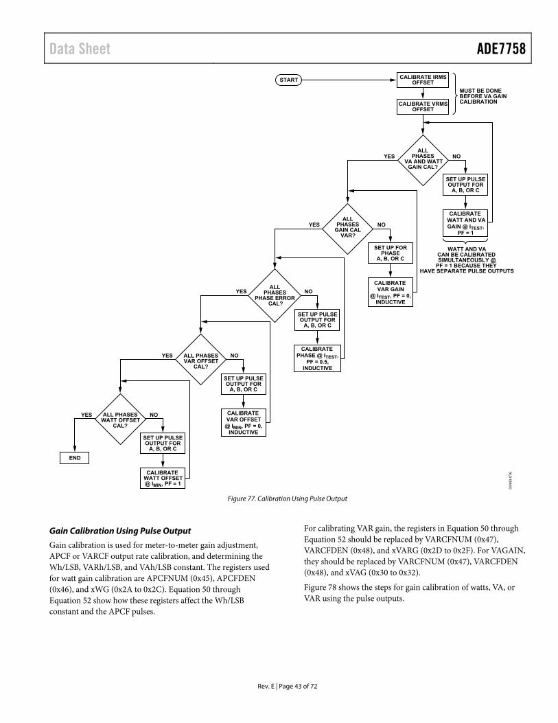
Data Sheet ADE7758
Rev. E | Page 43 of 72
START CALIBRATE IRMSOFFSET
CALIBRATE VRMSOFFSET
MUST BE DONEBEFORE VA GAINCALIBRATION
WATT AND VACAN BE CALIBRATEDSIMULTANEOUSLY @
PF = 1 BECAUSE THEYHAVE SEPARATE PULSE OUTPUTS
ALLPHASES
VA AND WATTGAIN CAL?
YES NO
SET UP PULSEOUTPUT FOR
A, B, OR C
CALIBRATEWATT AND VAGAIN @ ITEST,
PF = 1
ALLPHASES
GAIN CALVAR?
YES NO
SET UP FORPHASE
A, B, OR C
CALIBRATEVAR GAIN
@ ITEST, PF = 0,INDUCTIVE
ALLPHASES
PHASE ERROR CAL?
YES NO
SET UP PULSEOUTPUT FOR
A, B, OR C
CALIBRATEPHASE @ ITEST,
PF = 0.5,INDUCTIVE
ALL PHASESVAR OFFSET
CAL?
YES NO
SET UP PULSEOUTPUT FOR
A, B, OR C
CALIBRATEVAR OFFSET
@ IMIN, PF = 0,INDUCTIVE
ALL PHASESWATT OFFSET
CAL?
YES NO
SET UP PULSEOUTPUT FOR
A, B, OR C
CALIBRATEWATT OFFSET@ IMIN, PF = 1
END
0444
3-07
6
Figure 77. Calibration Using Pulse Output
Gain Calibration Using Pulse Output
Gain calibration is used for meter-to-meter gain adjustment, APCF or VARCF output rate calibration, and determining the Wh/LSB, VARh/LSB, and VAh/LSB constant. The registers used for watt gain calibration are APCFNUM (0x45), APCFDEN (0x46), and xWG (0x2A to 0x2C). Equation 50 through Equation 52 show how these registers affect the Wh/LSB constant and the APCF pulses.
For calibrating VAR gain, the registers in Equation 50 through Equation 52 should be replaced by VARCFNUM (0x47), VARCFDEN (0x48), and xVARG (0x2D to 0x2F). For VAGAIN, they should be replaced by VARCFNUM (0x47), VARCFDEN (0x48), and xVAG (0x30 to 0x32).
Figure 78 shows the steps for gain calibration of watts, VA, or VAR using the pulse outputs.
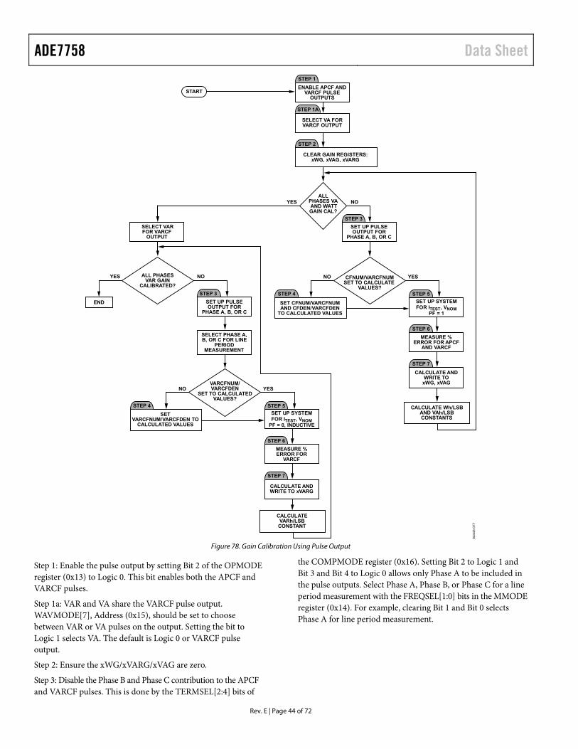
ADE7758 Data Sheet
Rev. E | Page 44 of 72
START
STEP 1
STEP 1A
ENABLE APCF ANDVARCF PULSE
OUTPUTS
STEP 2
CLEAR GAIN REGISTERS:xWG, xVAG, xVARG
SELECT VA FORVARCF OUTPUT
CFNUM/VARCFNUMSET TO CALCULATE
VALUES?
NO YES
ALLPHASES VAAND WATTGAIN CAL?
YES NO
STEP 3SET UP PULSEOUTPUT FOR
PHASE A, B, OR C
STEP 5SET UP SYSTEMFOR ITEST, VNOM
PF = 1
STEP 6MEASURE %
ERROR FOR APCFAND VARCF
STEP 7CALCULATE AND
WRITE TOxWG, xVAG
CALCULATE Wh/LSBAND VAh/LSBCONSTANTS
SET CFNUM/VARCFNUMAND CFDEN/VARCFDEN
TO CALCULATED VALUES
STEP 4END
ALL PHASESVAR GAIN
CALIBRATED?
YES NO
SELECT VARFOR VARCF
OUTPUT
STEP 3SET UP PULSEOUTPUT FOR
PHASE A, B, OR C
VARCFNUM/VARCFDEN
SET TO CALCULATEDVALUES?
NO YES
STEP 5SET UP SYSTEMFOR ITEST, VNOM
PF = 0, INDUCTIVE
STEP 6MEASURE %ERROR FOR
VARCF
STEP 7
CALCULATE ANDWRITE TO xVARG
CALCULATEVARh/LSB
CONSTANT
SETVARCFNUM/VARCFDEN TO
CALCULATED VALUES
STEP 4
0444
3-07
7
SELECT PHASE A,B, OR C FOR LINE
PERIODMEASUREMENT
Figure 78. Gain Calibration Using Pulse Output
Step 1: Enable the pulse output by setting Bit 2 of the OPMODE register (0x13) to Logic 0. This bit enables both the APCF and VARCF pulses.
Step 1a: VAR and VA share the VARCF pulse output. WAVMODE[7], Address (0x15), should be set to choose between VAR or VA pulses on the output. Setting the bit to Logic 1 selects VA. The default is Logic 0 or VARCF pulse output.
Step 2: Ensure the xWG/xVARG/xVAG are zero.
Step 3: Disable the Phase B and Phase C contribution to the APCF and VARCF pulses. This is done by the TERMSEL[2:4] bits of
the COMPMODE register (0x16). Setting Bit 2 to Logic 1 and Bit 3 and Bit 4 to Logic 0 allows only Phase A to be included in the pulse outputs. Select Phase A, Phase B, or Phase C for a line period measurement with the FREQSEL[1:0] bits in the MMODE register (0x14). For example, clearing Bit 1 and Bit 0 selects Phase A for line period measurement.
Data Sheet ADE7758
Rev. E | Page 45 of 72
Step 4: Set APCFNUM (0x45) and APCFDEN (0x46) to the calculated value to perform a coarse adjustment on the imp/kWh ratio. For VAR/VA calibration, set VARCFNUM (0x47) and VARCFDEN (0x48) to the calculated value.
The pulse output frequency with one phase at full-scale inputs is approximately 16 kHz. A sample set of meters could be tested to find a more exact value of the pulse output at full scale in the user application.
To calculate the values for APCFNUM/APCFDEN and VARCFNUM/VARCFDEN, use the following formulas:
FULLSCALE
TEST
FULLSCALE
NOMNOMINAL I
IV
VAPCF ××= kHz16 (45)
( )θ××
××= cos
36001000NOMTEST
EXPECTED
VIMCAPCF (46)
⎟⎠
⎞⎜⎝
⎛=
EXPECTED
NOMINAL
APCFAPCF
INTAPCFDEN (47)
where:
MC is the meter constant. ITEST is the test current. VNOM is the nominal voltage at which the meter is tested. VFULLSCALE and IFULLSCALE are the values of current and voltage, which correspond to the full-scale ADC inputs of the ADE7758. θ is the angle between the current and the voltage channel. APCFEXPECTED is equivalent to the reference meter output under the test conditions. APCFNUM is written to 0 or 1.
The equations for calculating the VARCFNUM and VARCFDEN during VAR calibration are similar:
( )θ××
××= sin
36001000NOMTEST
EXPECTED
VIMCVARCF (48)
Because the APCFDEN and VARCFDEN values can be calculated from the meter design, these values can be written to the part automatically during production calibration.
Step 5: Set the test system for ITEST, VNOM, and the unity power factor. For VAR calibration, the power factor should be set to 0 inductive in this step. For watt and VA, the unity power factor should be used. VAGAIN can be calibrated at the same time as WGAIN because VAGAIN can be calibrated at the unity power factor, and both pulse outputs can be measured simultaneously. However, when calibrating VAGAIN at the same time as WGAIN, the rms offsets should be calibrated first (see the Calibration of IRMS and VRMS Offset section).
Step 6: Measure the percent error in the pulse output, APCF and/or VARCF, from the reference meter:
%100–
% ×=REF
REF
CFCFAPCF
Error (49)
where CFREF = APCFEXPECTED = the pulse output of the reference meter.
Step 7: Calculate xWG adjustment. One LSB change in xWG (12 bits) changes the WATTHR register by 0.0244% and therefore APCF by 0.0244%. The same relationship holds true for VARCF.
[ ][ ]
[ ]⎟⎠⎞
⎜⎝⎛ +××
=
1220:111
0:110:11 xWG
APCFDENAPCFNUMAPCF
APCF
NOMINAL
EXPECTED
(50)
%0244.0%– ErrorxWG = (51)
When APCF is calibrated, the xWATTHR registers have the same Wh/LSB from meter to meter if the meter constant and the APCFNUM/APCFDEN ratio remain the same. The Wh/LSB constant is
WDIVAPCFNUMAPCFDENMCLSB
Wh1
10004
1
×××= (52)
Return to Step 2 to calibrate Phase B and Phase C gain.
Example: Watt Gain Calibration of Phase A Using Pulse Output
For this example, ITEST = 10 A, VNOM = 220 V, VFULLSCALE = 500 V, IFULLSCALE = 130 A, MC = 3200 impulses/kWh, Power Factor = 1, and Frequency = 50 Hz.
Clear APCFNUM (0x45) and write the calculated value to APCFDEN (0x46) to perform a coarse adjustment on the imp/kWh ratio, using Equation 45 through Equation 47.
kHz542.013010
500220kHz16 =××=NOMINALAPCF
( ) Hz9556.10cos36001000
220103200=×
×××
=EXPECTEDAPCF
277Hz9556.1
Hz542=⎟
⎟⎠
⎞⎜⎜⎝
⎛= INTAPCFDEN
With Phase A contributing to CF, at ITEST, VNOM, and the unity power factor, the example ADE7758 meter shows 2.058 Hz on the pulse output. This is equivalent to a 5.26% error from the reference meter value using Equation 49.
%26.5%100Hz9556.1
Hz9556.1–Hz058.2=×=%Error
The AWG value is calculated to be −216 d using Equation 51, which means the value 0xF28 should be written to AWG.
2802165.215%0244.0
%26.5– xFAWG =−=−==

ADE7758 Data Sheet
Rev. E | Page 46 of 72
PHASE CALIBRATION USING PULSE OUTPUT The ADE7758 includes a phase calibration register on each phase to compensate for small phase errors. Large phase errors should be compensated by adjusting the antialiasing filters. The ADE7758 phase calibration is a time delay with different weights in the positive and negative direction (see the Phase Compensation section). Because a current transformer is a source of phase error, a fixed nominal value can be decided on to load into the xPHCAL registers at power-up. During calibration, this value can be adjusted for CT-to-CT error. Figure 79 shows the steps involved in calibrating the phase using the pulse output.
START
ALLPHASES
PHASE ERRORCALIBRATED?
END
YES NO
STEP 1
SET UP PULSEOUTPUT FOR
PHASE A, B, OR CAND ENABLE CF
OUTPUTS
STEP 2
SET UP SYSTEMFOR ITEST, VNOM,
PF = 0.5, INDUCTIVE
STEP 3
MEASURE %ERROR IN APCF
STEP 4
CALCULATE PHASEERROR (DEGREES)
STEP 5
PERIOD OFSYSTEMKNOWN?
MEASUREPERIOD USING
FREQ[11:0]REGISTER
NO YES
CALCULATE ANDWRITE TOxPHCAL
0444
3-07
8
SELECT PHASEFOR LINE PERIODMEASUREMENT
CONFIGUREFREQ[11:0] FOR A
LINE PERIODMEASUREMENT
Figure 79. Phase Calibration Using Pulse Output
Step 1: Step 1 and Step 3 from the gain calibration should be repeated to configure the ADE7758 pulse output. Ensure the xPHCAL registers are zero.
Step 2: Set the test system for ITEST, VNOM, and 0.5 power factor inductive.
Step 3: Measure the percent error in the pulse output, APCF, from the reference meter using Equation 49.
Step 4: Calculate the Phase Error in degrees by
3%100
–%Error
ArcsinErrorPhase (53)
Step 5: Calculate xPHCAL.
3601
)(1
__1
sPeriodLineWeightLSBPHCALErrorPhase
xPHCAL(54)
where PHCAL_LSB_Weight is 1.2 μs if the %Error is negative or 2.4 μs if the %Error is positive (see the Phase Compensation section).
If it is not known, the line period is available in the ADE7758 frequency register, FREQ (0x10). To configure line period measurement, select the phase for period measurement in the MMODE[1:0] and set LCYCMODE[7]. Equation 55 shows how to determine the value that needs to be written to xPHCAL using the period register measurement.
360]0:11[
__6.9 FREQ
WeightLSBPHCALs
ErrorPhase
xPHCAL (55)
Example: Phase Calibration of Phase A Using Pulse Output
For this example, ITEST = 10 A, VNOM = 220 V, VFULLSCALE = 500 V, IFULLSCALE = 130 A, MC = 3200 impulses/kWh, power factor = 0.5 inductive, and frequency = 50 Hz.
With Phase A contributing to CF, at ITEST, VNOM, and 0.5 inductive power factor, the example ADE7758 meter shows 0.9668 Hz on the pulse output. This is equivalent to −1.122% error from the reference meter value using Equation 49.
The Phase Error in degrees using Equation 53 is 0.3713°.
3713.0
3%1001.122%–– ArcsinErrorPhase
If at 50 Hz the FREQ register = 2083d, the value that should be written to APHCAL is 17d, or 0x11 using Equation 55. Note that a PHCAL_LSB_Weight of 1.2 μs is used because the %Error is negative.
1101719.173602083
μs2.1μs6.9
3713.0 xAPHCAL
Power Offset Calibration Using Pulse Output
Power offset calibration should be used for outstanding performance over a wide dynamic range (1000:1). Calibration of the power offset is done at or close to the minimum current where the desired accuracy is required.
The ADE7758 has power offset registers for watts and VAR (xWATTOS and xVAROS). Offsets in the VA measurement are compensated by adjusting the rms offset registers (see the Calibration of IRMS and VRMS Offset section). Figure 80 shows the steps to calibrate the power offsets using the pulse outputs.

Data Sheet ADE7758
Rev. E | Page 47 of 72
START
STEP 1
ENABLE CFOUTPUTS
STEP 2CLEAR OFFSET
REGISTERSxWATTOS, xVAROS
ALL PHASESWATT OFFSETCALIBRATED?
YES NO
ALL PHASESVAR OFFSET
CALIBRATED?
YES NO
SET UP APCFPULSE OUTPUT
FOR PHASE A, B,OR C
STEP 4
STEP 3
SET UP SYSTEMFOR IMIN, VNOM,
PF = 1
STEP 5MEASURE %ERROR FOR
APCF
STEP 6CALCULATE AND
WRITE TOxWATTOS
END SET UP VARCFPULSE OUTPUT
FOR PHASE A, B,OR C
STEP 4
STEP 3
SET UP SYSTEMFOR IMIN, VNOM,
PF = 0, INDUCTIVE
STEP 5MEASURE %
ERROR FOR VARCF
MEASURE PERIODUSING FREQ[11:0]
REGISTER
STEP 6CALCULATE AND
WRITE TOxVAROS
STEP 7.REPEAT STEP3 TO STEP 6FOR xVAROS
SELECT PHASEFOR LINE PERIODMEASUREMENT
CONFIGUREFREQ[11:0] FOR A
LINE PERIODMEASUREMENT
0444
3-07
9
Figure 80. Offset Calibration Using Pulse Output
Step 1: Repeat Step 1 and Step 3 from the gain calibration to configure the ADE7758 pulse output.
Step 2: Clear the xWATTOS and xVAROS registers.
Step3: Disable the Phase B and Phase C contribution to the APCF and VARCF pulses. This is done by the TERMSEL[2:4] bits of the COMPMODE register (0x16). Setting Bit 2 to Logic 1 and Bit 3 and Bit 4 to Logic 0 allows only Phase A to be included in the pulse outputs. Select Phase A, Phase B, or Phase C for a line period measurement with the FREQSEL[1:0] bits in the MMODE register (0x14). For example, clearing Bit 1 and Bit 0 selects Phase A for line period measurement.
Step 4: Set the test system for IMIN, VNOM, and unity power factor. For Step 6, set the test system for IMIN, VNOM, and zero-power factor inductive.
Step 5: Measure the percent error in the pulse output, APCF or VARCF, from the reference meter using Equation 49.
Step 6: Calculate xWATTOS using Equation 56 (for xVAROS use Equation 57).
APCFNUMAPCFDEN
QAPCF
%APCF
xWATTOS
EXPECTEDERROR ××⎟
⎠⎞
⎜⎝⎛ ×
=42
%100–
(56)
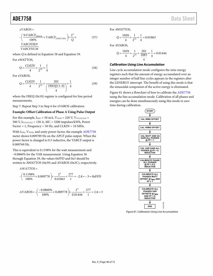
ADE7758 Data Sheet
Rev. E | Page 48 of 72
VARCFNUMVARCFDEN
QVARCF
%VARCF
xVAROS
EXPECTEDERROR ××⎟
⎠⎞
⎜⎝⎛ ×
=42
%100– (57)
where Q is defined in Equation 58 and Equation 59.
For xWATTOS,
41
21
4 25 ××=CLKINQ (58)
For xVAROS,
41
40]:[11
20221
4 24 ×⎟⎠⎞
⎜⎝⎛
××=FREQ
CLKINQ (59)
where the FREQ (0x10) register is configured for line period measurements.
Step 7: Repeat Step 3 to Step 6 for xVAROS calibration.
Example: Offset Calibration of Phase A Using Pulse Output
For this example, IMIN = 50 mA, VNOM = 220 V, VFULLSCALE = 500 V, IFULLSCALE = 130 A, MC = 3200 impulses/kWh, Power Factor = 1, Frequency = 50 Hz, and CLKIN = 10 MHz.
With IMIN, VNOM, and unity power factor, the example ADE7758 meter shows 0.009789 Hz on the APCF pulse output. When the power factor is changed to 0.5 inductive, the VARCF output is 0.009769 Hz.
This is equivalent to 0.1198% for the watt measurement and −0.0860% for the VAR measurement. Using Equation 56 through Equation 59, the values 0xFFD and 0x3 should be written to AWATTOS (0x39) and AVAROS (0x3C), respectively.
0xFFD3– –2.81
2770.01863
20.009778%100
0.1198%–4
===××⎟⎠⎞
⎜⎝⎛ ×
=AWATTOS
32.61
2770.01444
20.009778%100
0.0860%––4
==××⎟⎠⎞
⎜⎝⎛ ×=AVAROS
For AWATTOS,
01863.041
21
4610
25 =××=EQ
For AVAROS,
0.0144441
42083202
21
4610
24 =×××=EQ
Calibration Using Line Accumulation
Line cycle accumulation mode configures the nine energy registers such that the amount of energy accumulated over an integer number of half line cycles appears in the registers after the LENERGY interrupt. The benefit of using this mode is that the sinusoidal component of the active energy is eliminated.
Figure 81 shows a flowchart of how to calibrate the ADE7758 using the line accumulation mode. Calibration of all phases and energies can be done simultaneously using this mode to save time during calibration.
START
CAL IRMS OFFSET
CAL VRMS OFFSET
CAL WATT AND VAGAIN ALL PHASES
@ PF = 1
CAL VAR GAIN ALLPHASES @ PF = 0,
INDUCTIVE
CALIBRATE PHASEALL PHASES@ PF = 0.5,INDUCTIVE
CALIBRATE ALLPHASES WATT
OFFSET @ IMIN ANDPF = 1
CALIBRATE ALLPHASES VAR
OFFSETS @ IMINAND PF = 0,INDUCTIVE
END
0444
3-08
0
Figure 81. Calibration Using Line Accumulation
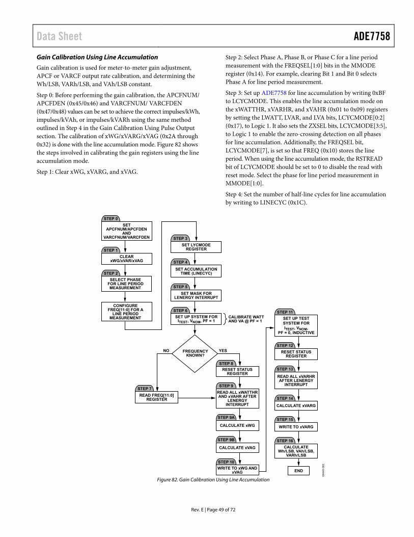
Data Sheet ADE7758
Rev. E | Page 49 of 72
Gain Calibration Using Line Accumulation Step 2: Select Phase A, Phase B, or Phase C for a line period measurement with the FREQSEL[1:0] bits in the MMODE register (0x14). For example, clearing Bit 1 and Bit 0 selects Phase A for line period measurement.
Gain calibration is used for meter-to-meter gain adjustment, APCF or VARCF output rate calibration, and determining the Wh/LSB, VARh/LSB, and VAh/LSB constant.
Step 3: Set up ADE7758 for line accumulation by writing 0xBF to LCYCMODE. This enables the line accumulation mode on the xWATTHR, xVARHR, and xVAHR (0x01 to 0x09) registers by setting the LWATT, LVAR, and LVA bits, LCYCMODE[0:2] (0x17), to Logic 1. It also sets the ZXSEL bits, LCYCMODE[3:5], to Logic 1 to enable the zero-crossing detection on all phases for line accumulation. Additionally, the FREQSEL bit, LCYCMODE[7], is set so that FREQ (0x10) stores the line period. When using the line accumulation mode, the RSTREAD bit of LCYCMODE should be set to 0 to disable the read with reset mode. Select the phase for line period measurement in MMODE[1:0].
Step 0: Before performing the gain calibration, the APCFNUM/ APCFDEN (0x45/0x46) and VARCFNUM/ VARCFDEN (0x47/0x48) values can be set to achieve the correct impulses/kWh, impulses/kVAh, or impulses/kVARh using the same method outlined in Step 4 in the Gain Calibration Using Pulse Output section. The calibration of xWG/xVARG/xVAG (0x2A through 0x32) is done with the line accumulation mode. Figure 82 shows the steps involved in calibrating the gain registers using the line accumulation mode.
Step 1: Clear xWG, xVARG, and xVAG.
Step 4: Set the number of half-line cycles for line accumulation by writing to LINECYC (0x1C).
FREQUENCYKNOWN?
NO YES
STEP 0SET
APCFNUM/APCFDENAND
VARCFNUM/VARCFDEN
STEP 1
STEP 2
CLEARxWG/xVAR/xVAG
STEP 3SET LYCMODE
REGISTER
STEP 4SET ACCUMULATION
TIME (LINECYC)
STEP 5SET MASK FOR
LENERGY INTERRUPT
STEP 6SET UP SYSTEM FOR
ITEST, VNOM, PF = 1
STEP 7READ FREQ[11:0]
REGISTER
STEP 8RESET STATUS
REGISTER
STEP 9READ ALL xWATTHRAND xVAHR AFTER
LENERGYINTERRUPT
STEP 9A
CALCULATE xWG
STEP 9B
CALCULATE xVAG
STEP 10WRITE TO xWG AND
xVAG
CALIBRATE WATTAND VA @ PF = 1
STEP 11SET UP TESTSYSTEM FORITEST, VNOM,
PF = 0, INDUCTIVE
STEP 12RESET STATUS
REGISTER
STEP 13
READ ALL xVARHRAFTER LENERGY
INTERRUPT
STEP 14
CALCULATE xVARG
STEP 15
WRITE TO xVARG
STEP 16CALCULATE
Wh/LSB, VAh/LSB,VARh/LSB
END
0444
3-08
1
SELECT PHASEFOR LINE PERIODMEASUREMENT
CONFIGUREFREQ[11:0] FOR A
LINE PERIODMEASUREMENT
Figure 82. Gain Calibration Using Line Accumulation
ADE7758 Data Sheet
Rev. E | Page 50 of 72
Step 5: Set the LENERGY bit, MASK[12] (0x18), to Logic 1 to enable the interrupt signaling the end of the line cycle accumulation.
Step 6: Set the test system for ITEST, VNOM, and unity power factor (calibrate watt and VA simultaneously and first).
Step 7: Read the FREQ (0x10) register if the line frequency is unknown.
Step 8: Reset the interrupt status register by reading RSTATUS (0x1A).
Step 9: Read all six xWATTHR (0x01 to 0x03) and xVAHR (0x07 to 0x09) energy registers after the LENERGY interrupt and store the values.
Step 9a: Calculate the values to be written to xWG registers according to the following equations:
( )
WDIVAPCFNUMAPCFDEN
AccumTimeθcosVIMCWATTHR
NOMTEST
EXPECTED
136001000
4
×
××
×××××
=
(60)
where AccumTime is
[ ]SelectedPhasesofNo.FrequencyLine
:LINECYC××2
015 (61)
where:
MC is the meter constant.
θ is the angle between the current and voltage.
Line Frequency is known or calculated from the FREQ[11:0] register. With the FREQ[11:0] register configured for line period measurements, the line frequency is calculated with Equation 62.
6-109.60]:[111
××=
FREQFrequencyLine (62)
No. of Phases Selected is the number of ZXSEL bits set to Logic 1 in LCYCMODE (0x17).
Then, xWG is calculated as
1221 ×⎟⎟⎠
⎞⎜⎜⎝
⎛−=
MEASURED
EXPECTED
WATTHRWATTHR
xWG (63)
Step 9b: Calculate the values to be written to the xVAG registers according to the following equation:
VADIVVARCFNUMVARCFDENAccumTimeVIMC
VAHR
NOMTEST
EXPECTED
136001000
4××
×××××
=
(64)
1221 ×⎟⎟⎠
⎞⎜⎜⎝
⎛−=
MEASURED
EXPECTED
VAHRVAHR
xVAG
Step 10: Write to xWG and xVAG.
Step 11: Set the test system for ITEST, VNOM, and zero power factor inductive to calibrate VAR gain.
Step 12: Repeat Step 7.
Step 13: Read the xVARHR (0x04 to 0x06) after the LENERGY interrupt and store the values.
Step 14: Calculate the values to be written to the xVARG registers (to adjust VARCF to the expected value).
( )
VARDIVVARCFNUMVARCFDEN
AccumTimeθsinVIMCVARHR
NOMTEST
EXPECTED
136001000
4
×
××
×××××
=
(65)
1221 ×⎟⎟⎠
⎞⎜⎜⎝
⎛−=
MEASURED
EXPECTED
VARHRVARHR
xVARG
Step 15: Write to xVARG.
Step 16: Calculate the Wh/LSB, VARh/LSB, and VAh/LSB constants.
( )xWATTHR
AccumTimeθcosVILSBWh NOMTEST
××××
=3600
(66)
xVAHRAccumTimeVI
LSBVAh NOMTEST
×××
=3600
(67)
( )xVARHR
AccumTimeθsinVILSB
VARh NOMTEST
××××
=3600
(68)
Example: Watt Gain Calibration Using Line Accumulation
This example shows only Phase A watt calibration. The steps outlined in the Gain Calibration Using Line Accumulation section show how to calibrate watt, VA, and VAR. All three phases can be calibrated simultaneously because there are nine energy registers.
For this example, ITEST = 10 A, VNOM = 220 V, Power Factor = 1, Frequency = 50 Hz, LINECYC (0x1C) is set to 0x800, and MC = 3200 imp/kWhr.

Data Sheet ADE7758
Rev. E | Page 51 of 72
To set APCFNUM (0x45) and APCFDEN (0x46) to the calculated value to perform a coarse adjustment on the imp/kW-hr ratio, use Equation 45 to Equation 47.
kHz5415.013010
500220kH16 =××= zAPCFNOMINAL
( ) Hz1.956cos36001000
220103200=θ×
×××
=EXPECTEDAPCF
277Hz956.1Hz5.541
INT =⎟⎟⎠
⎞⎜⎜⎝
⎛=APCFDEN
Under the test conditions above, the AWATTHR register value is 15559d after the LENERGY interrupt. Using Equation 60 and Equation 61, the value to be written to AWG is −199d, 0xF39.
[ ]
SelectedPhasesofNo.FREQ
:LINECYCAccumTime×
×××
=−6106.9]0:11[
12
015
6.832128s3
106.9208512
8000
6
=×
×××
=−
xAccumTime
1480411
27736001000
832.612201032004=××
××××××
=EXPECTEDWATTHR
0xF39–199–198.87640211555914804 12 ===×⎟
⎠⎞
⎜⎝⎛ −=xWG
Using Equation 66, the Wh/LSB constant is
00.000282148043600
832.622010=
×××
=LSBWh
Phase Calibration Using Line Accumulation
The ADE7758 includes a phase calibration register on each phase to compensate for small phase errors. Large phase errors should be compensated by adjusting the antialiasing filters. The ADE7758 phase calibration is a time delay with different weights in the positive and negative direction (see the Phase Compensation section). Because a current transformer is a source of phase error, a fixed nominal value can be decided on to load into the xPHCAL (0x3F to 0x41) registers at power-up. During calibration, this value can be adjusted for CT-to-CT error. Figure 83 shows the steps involved in calibrating the phase using the line accumulation mode.
STEP 1SET LCYCMODE,
LINECYC AND MASKREGISTERS
STEP 2SET UP SYSTEM FORITEST, VNOM, PF = 0.5,
INDUCTIVE
STEP 3RESET STATUS
REGISTER
STEP 4READ ALL xWATTHRREGISTERS AFTER
LENERGYINTERRUPT
STEP 5CALCULATE PHASEERROR IN DEGREES
FOR ALL PHASES
STEP 6CALCULATE AND
WRITE TO ALLxPHCAL REGISTERS 04
443-
082
Figure 83. Phase Calibration Using Line Accumulation
Step 1: If the values were changed after gain calibration, Step 1, Step 3, and Step 4 from the gain calibration should be repeated to configure the LCYCMODE and LINECYC registers.
Step 2: Set the test system for ITEST, VNOM, and 0.5 power factor inductive.
Step 3: Reset the interrupt status register by reading RSTATUS (0x1A).
Step 4: The xWATTHR registers should be read after the LENERGY interrupt. Measure the percent error in the energy register readings (AWATTHR, BWATTHR, and CWATTHR) compared to the energy register readings at unity power factor (after gain calibration) using Equation 69. The readings at unity power factor should have been repeated after the gain calibration and stored for use in the phase calibration routine.
2
2–
1PF
1PF5PF
=
==
= xWATTHR
xWATTHRxWATTHR
Error (69)
Step 5: Calculate the Phase Error in degrees using the equation
( ) ⎟⎠⎞
⎜⎝⎛=°
3– ErrorArcsinErrorPhase (70)
Step 6: Calculate xPHCAL and write to the xPHCAL registers (0x3F to 0x41).
°×××
=
3601
)(1
__1
sPeriodLineWeightLSBPHCALErrorPhase
xPHCAL(71)
where PHCAL_LSB_Weight is 1.2 μs if the %Error is negative or 2.4 μs if the %Error is positive (see the Phase Compensation section).

ADE7758 Data Sheet
Rev. E | Page 52 of 72
If it is not known, the line period is available in the ADE7758 frequency register, FREQ (0x10). To configure line period measurement, select the phase for period measurement in the MMODE[1:0] and set LCYCMODE[7]. Equation 72 shows how to determine the value that needs to be written to xPHCAL using the period register measurement.
°××
=
360]0:11[
__μs6.9 FREQ
WeightLSBPHCALErrorPhase
xPHCAL (72)
Example: Phase Calibration Using Line Accumulation
This example shows only Phase A phase calibration. All three PHCAL registers can be calibrated simultaneously using the same method.
For this example, ITEST = 10 A, VNOM = 220 V, power factor = 0.5 inductive, and frequency = 50 Hz. Also, LINECYC = 0x800.
With ITEST, VNOM, and 0.5 inductive power factor, the example ADE7758 meter shows 7318d in the AWATTHR (0x01) register.
14804d in the AWATTHR register. This is equivalent to −1.132% error.
%132.101132.0
214804
214804–7318
−=−==Error
The Phase Error in degrees using Equation 66 is 0.374°.
( ) °=⎟⎠
⎞⎛ − 01132.0⎜⎝
=° 374.03
sin–ArcErrorPhase
Using Equation 72, the value written to APHCAL (0x3F), if at 50 Hz, the FREQ (0x10) register = 2085d, is 17d. Note that a PHCAL_LSB_Weight of 1.2 μs is used because the %Error is negative.
11x017360
20852.16.9374.0 ==××°=APHCAL
For unity power factor (after gain calibration), the meter shows
STEP 1
SET MMODE,LCYCMODE,
LINECYC ANDMASK REGISTERS
STEP 2SET UP SYSTEMFOR IMIN, VNOM
@ PF = 1
STEP 3RESET STATUS
REGISTER
STEP 4READ ALLxWATTHR
REGISTERS AFTERLENERGY
INTERRUPT
END
FOR STEP 8READ ALL xVARHR
AFTER LENERGYINTERRUPT
FOR STEP 8, CALCULATExVAROS FOR ALL PHASES
STEP 5CALCULATE
xWATTOS FOR ALLPHASES
FOR STEP 8, WRITE TOALL xVAROS REGISTERS
STEP 6WRITE TO ALL
xWATTOSREGISTERS
STEP 7SET UP SYSTEM
FOR ITEST, VNOM @PF = 0, INDUCTIVE
STEP 8REPEAT STEP 3 TO
STEP 8 FORxVARHR, xVAROS
CALIBRATION 0444
3-08
3
Figure 84. Power Offset Calibration Using Line Accumulation
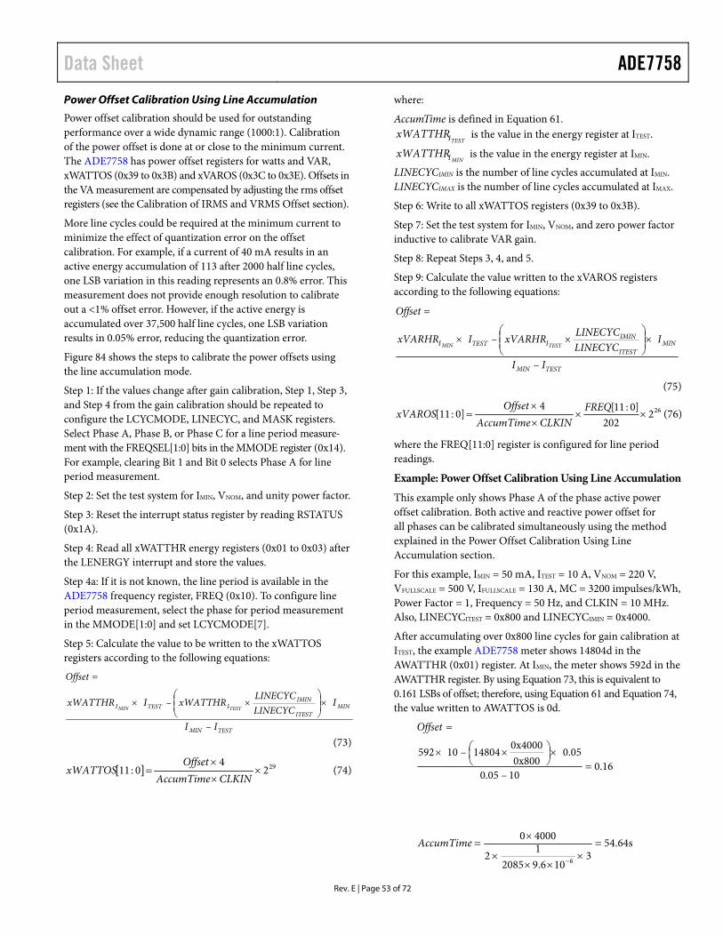
Data Sheet ADE7758
Rev. E | Page 53 of 72
Power Offset Calibration Using Line Accumulation
Power offset calibration should be used for outstanding performance over a wide dynamic range (1000:1). Calibration of the power offset is done at or close to the minimum current. The ADE7758 has power offset registers for watts and VAR, xWATTOS (0x39 to 0x3B) and xVAROS (0x3C to 0x3E). Offsets in the VA measurement are compensated by adjusting the rms offset registers (see the Calibration of IRMS and VRMS Offset section).
More line cycles could be required at the minimum current to minimize the effect of quantization error on the offset calibration. For example, if a current of 40 mA results in an active energy accumulation of 113 after 2000 half line cycles, one LSB variation in this reading represents an 0.8% error. This measurement does not provide enough resolution to calibrate out a <1% offset error. However, if the active energy is accumulated over 37,500 half line cycles, one LSB variation results in 0.05% error, reducing the quantization error.
Figure 84 shows the steps to calibrate the power offsets using the line accumulation mode.
Step 1: If the values change after gain calibration, Step 1, Step 3, and Step 4 from the gain calibration should be repeated to configure the LCYCMODE, LINECYC, and MASK registers. Select Phase A, Phase B, or Phase C for a line period measure-ment with the FREQSEL[1:0] bits in the MMODE register (0x14). For example, clearing Bit 1 and Bit 0 selects Phase A for line period measurement.
Step 2: Set the test system for IMIN, VNOM, and unity power factor.
Step 3: Reset the interrupt status register by reading RSTATUS (0x1A).
Step 4: Read all xWATTHR energy registers (0x01 to 0x03) after the LENERGY interrupt and store the values.
Step 4a: If it is not known, the line period is available in the ADE7758 frequency register, FREQ (0x10). To configure line period measurement, select the phase for period measurement in the MMODE[1:0] and set LCYCMODE[7].
Step 5: Calculate the value to be written to the xWATTOS registers according to the following equations:
TESTMIN
MINITEST
IMINITESTI
II
ILINECYCLINECYC
xWATTHRIxWATTHR
Offset
TESTMIN
–
– ×⎟⎟⎠
⎞⎜⎜⎝
⎛××
=
(73)
[ ] 2924
0:11 ×××
=CLKINAccumTime
OffsetxWATTOS (74)
where:
AccumTime is defined in Equation 61. is the value in the energy register at ITEST.
is the value in the energy register at IMIN.
LINECYCIMIN is the number of line cycles accumulated at IMIN. LINECYCIMAX is the number of line cycles accumulated at IMAX.
TESTIxWATTHR
MINIxWATTHR
Step 6: Write to all xWATTOS registers (0x39 to 0x3B).
Step 7: Set the test system for IMIN, VNOM, and zero power factor inductive to calibrate VAR gain.
Step 8: Repeat Steps 3, 4, and 5.
Step 9: Calculate the value written to the xVAROS registers according to the following equations:
TESTMIN
MINITEST
IMINITESTI
II
ILINECYCLINECYCxVARHRIxVARHR
Offset
TESTMIN
–
– ×⎟⎟⎠
⎞⎜⎜⎝
⎛××
=
(75)
262202
]0:11[40]:[11 ××
××
=FREQ
CLKINAccumTimeOffset
xVAROS (76)
where the FREQ[11:0] register is configured for line period readings.
Example: Power Offset Calibration Using Line Accumulation
This example only shows Phase A of the phase active power offset calibration. Both active and reactive power offset for all phases can be calibrated simultaneously using the method explained in the Power Offset Calibration Using Line Accumulation section.
For this example, IMIN = 50 mA, ITEST = 10 A, VNOM = 220 V, VFULLSCALE = 500 V, IFULLSCALE = 130 A, MC = 3200 impulses/kWh, Power Factor = 1, Frequency = 50 Hz, and CLKIN = 10 MHz. Also, LINECYCITEST = 0x800 and LINECYCIMIN = 0x4000.
After accumulating over 0x800 line cycles for gain calibration at ITEST, the example ADE7758 meter shows 14804d in the AWATTHR (0x01) register. At IMIN, the meter shows 592d in the AWATTHR register. By using Equation 73, this is equivalent to 0.161 LSBs of offset; therefore, using Equation 61 and Equation 74, the value written to AWATTOS is 0d.
0.1610–0.05
0.050x800
0x400014804–10592=
×⎟⎠⎞
⎜⎝⎛ ××
=Offset
s64.453
106.9208512
40000
6
=×
×××
×=
−
AccumTime
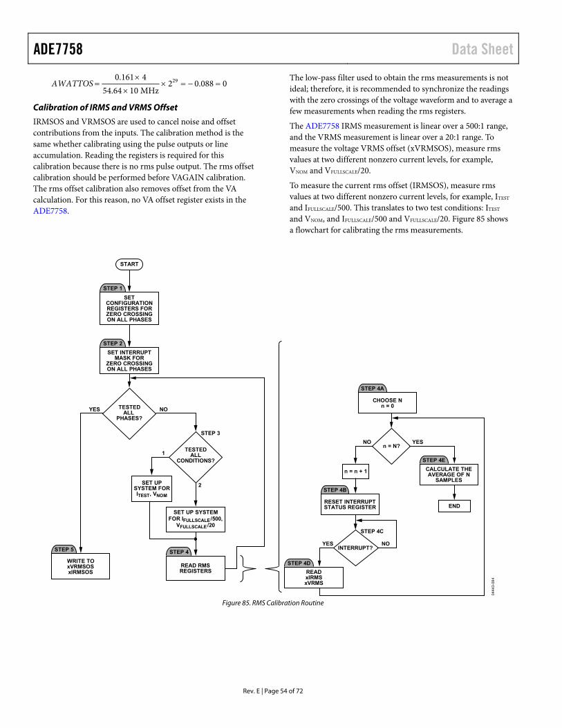
ADE7758 Data Sheet
Rev. E | Page 54 of 72
00.0882MHz1054.6440.161 29 =−=×
××
=AWATTOS The low-pass filter used to obtain the rms measurements is not ideal; therefore, it is recommended to synchronize the readings with the zero crossings of the voltage waveform and to average a few measurements when reading the rms registers. Calibration of IRMS and VRMS Offset
IRMSOS and VRMSOS are used to cancel noise and offset contributions from the inputs. The calibration method is the same whether calibrating using the pulse outputs or line accumulation. Reading the registers is required for this calibration because there is no rms pulse output. The rms offset calibration should be performed before VAGAIN calibration. The rms offset calibration also removes offset from the VA calculation. For this reason, no VA offset register exists in the ADE7758.
The ADE7758 IRMS measurement is linear over a 500:1 range, and the VRMS measurement is linear over a 20:1 range. To measure the voltage VRMS offset (xVRMSOS), measure rms values at two different nonzero current levels, for example, VNOM and VFULLSCALE/20.
To measure the current rms offset (IRMSOS), measure rms values at two different nonzero current levels, for example, ITEST
and IFULLSCALE/500. This translates to two test conditions: ITEST and VNOM, and IFULLSCALE/500 and VFULLSCALE/20. Figure 85 shows a flowchart for calibrating the rms measurements.
STEP 1SET
CONFIGURATIONREGISTERS FORZERO CROSSINGON ALL PHASES
STEP 2SET INTERRUPT
MASK FORZERO CROSSINGON ALL PHASES
STEP 3
STEP 4
READ RMSREGISTERS
STEP 5
WRITE TOxVRMSOSxIRMSOS
SET UPSYSTEM FORITEST, VNOM
SET UP SYSTEMFOR IFULLSCALE/500,
VFULLSCALE/20
START
TESTEDALL
PHASES?YES NO
TESTEDALL
CONDITIONS?1
2
STEP 4A
CHOOSE Nn = 0
STEP 4DREADxIRMSxVRMS
STEP 4ECALCULATE THEAVERAGE OF N
SAMPLES
STEP 4B
RESET INTERRUPTSTATUS REGISTER END
n = n + 1
n = N?NO YES
YES NO
STEP 4C
INTERRUPT?
0444
3-08
4
Figure 85. RMS Calibration Routine
Data Sheet ADE7758
Rev. E | Page 55 of 72
Step 1: Set configuration registers for zero crossings on all phases by writing the value 0x38 to the LCYCMODE register (0x17). This sets all of the ZXSEL bits to Logic 1.
Step 2: Set the interrupt mask register for zero-crossing detection on all phases by writing 0xE00 to the MASK[0:24] register (0x18). This sets all of the ZX bits to Logic 1.
Step 3: Set up the calibration system for one of the two test conditions: ITEST and VNOM, and IFULLSCALE/500 and VFULLSCALE/20.
Step 4: Read the rms registers after the zero-crossing interrupt and take an average of N samples. This is recommended to get the most stable rms readings. This procedure is detailed in Figure 85: Steps 4a through 4e.
Step 4a. Choose the number of samples, N, to be averaged.
Step 4b. Reset the interrupt status register by reading RSTATUS (0x1A).
Step 4c. Wait for the zero-crossing interrupt. When the zero-crossing interrupt occurs, move to Step 4d.
Step 4d. Read the xIRMS and xVRMS registers. These values will be averaged in Step 4e.
Step 4e: Average the N samples of xIRMS and xVRMS. The averaged values will be used in Step 5.
Step 5: Write to the xVRMSOS (0x33 to 0x35) and xIRMSOS (0x36 to 0x38) registers according to the following equations:
( ) ( )22
2222
163841
TESTMIN
ITESTMINIMINTEST
I–IIRMSI–IRMSI
xIRMSOS
×××
=
(77)
where:
IMIN is the full scale current/500. ITEST is the test current.
IRMSIMIN and IRMSITEST are the current rms register values without offset correction for the inputs IMIN and ITEST, respectively.
NOMMIN
VNOMMINVMINNOM
V–VVRMSV–VRMSV
xVRMSOS××
×
=
641
(78)
where:
VMIN is the full scale voltage/20 VNOM is the nominal line voltage.
VRMSVMIN and VRMSVNOM are the voltage rms register values without offset correction for the input VMIN and VNOM, respectively.
Example: Calibration of RMS Offsets
For this example, ITEST = 10 A, IMAX = 100 A, VNOM = 220 V, VFULLSCALE = 500 V, Power Factor = 1, and Frequency = 50 Hz.
Twenty readings are taken synchronous to the zero crossings of all three phases at each current and voltage to determine the average xIRMS and xVRMS readings. At ITEST and VNOM, the example ADE7758 meter gets an average AIRMS (0x0A) reading of 148242.2 and 744570.8 in the AVRMS (0x0D) register. Then the current is set to IMIN = IFULLSCALE/500 or 260 mA. At IMIN, the average AIRMS reading is 3885.68. At VMIN = VFULLSCALE/20 or 25 V, the example meter gets an average AVRMS of 86362.36. Using this data, −15d is written to AIRMSOS (0x36) and −31d is written to AVRMSOS (0x33) registers according to the Equation 77 and Equation 78.
( ) (( )
)
0xFF2158.1410–260.0
148242.2260.0–3885.681016384
12
2222
=−=−
=××
×
=AIRMSOS
( ) ( )( ) 0xFE1319.30
220–25744570.825–86362.36220
641
=−=−=××
×
=AVRMSOS
This example shows the calculations and measurements for Phase A only. However, all three xIRMS and xVRMS registers can be read simultaneously to compute the values for each xIRMSOS and xVRMSOS register.
CHECKSUM REGISTER The ADE7758 has a checksum register CHKSUM[7:0] (0x7E) to ensure the data bits received in the last serial read operation are not corrupted. The 8-bit checksum register is reset before the first bit (MSB of the register to be read) is put on the DOUT pin. During a serial read operation, when each data bit becomes available on the rising edge of SCLK, the bit is added to the checksum register. In the end of the serial read operation, the contents of the checksum register are equal to the sum of all the 1s in the register previously read. Using the checksum register, the user can determine if an error has occurred during the last read operation. Note that a read to the checksum register also generates a checksum of the checksum register itself.
DOUT
ADDR: 0x7ECHECKSUMREGISTER
CONTENT OF REGISTERS(N-BYTES)
0444
3-08
5
Figure 86. Checksum Register for Serial Interface Read
INTERRUPTS The ADE7758 interrupts are managed through the interrupt status register (STATUS[23:0], Address 0x19) and the interrupt mask register (MASK[23:0], Address 0x18). When an interrupt event occurs in the ADE7758, the corresponding flag in the interrupt status register is set to a Logic 1 (see Table 24). If the mask bit for this interrupt in the interrupt mask register is Logic 1, then the IRQ logic output goes active low. The flag bits
ADE7758 Data Sheet
Rev. E | Page 56 of 72
in the interrupt status register are set irrespective of the state of the mask bits. To determine the source of the interrupt, the MCU should perform a read from the reset interrupt status register with reset. This is achieved by carrying out a read from RSTATUS, Address 0x1A. The IRQ output goes logic high on completion of the interrupt status register read command (see the section). When carrying out a read with reset, the is designed to ensure that no interrupt events are missed. If an interrupt event occurs just as the interrupt status register is being read, the event is not lost, and the
Interrupt TimingADE7758
IRQ logic output is guaranteed to go logic high for the duration of the interrupt status register data transfer before going logic low again to indicate the pending interrupt. Note that the reset interrupt bit in the status register is high for only one clock cycle, and it then goes back to 0.
USING THE INTERRUPTS WITH AN MCU Figure 87 shows a timing diagram that illustrates a suggested implementation of ADE7758 interrupt management using an MCU. At time t1, the IRQ line goes active low indicating that one or more interrupt events have occurred in the . The
ADE7758IRQ logic output should be tied to a negative-edge-
triggered external interrupt on the MCU. On detection of the negative edge, the MCU should be configured to start executing its interrupt service routine (ISR). On entering the ISR, all interrupts should be disabled using the global interrupt mask bit. At this point, the MCU external interrupt flag can be cleared to capture interrupt events that occur during the current ISR. When the MCU interrupt flag is cleared, a read from the reset interrupt status register with reset is carried out. (This causes the IRQ line to be reset logic high (t2); see the
section.) The reset interrupt status register contents are used to determine the source of the interrupt(s) and hence the appropriate action to be taken. If a subsequent interrupt event occurs during the ISR (t3) that event is recorded by the MCU external interrupt flag being set again.
Interrupt Timing
On returning from the ISR, the global interrupt mask bit is cleared (same instruction cycle) and the external interrupt flag uses the MCU to jump to its ISR once again. This ensures that the MCU does not miss any external interrupts. The reset bit in the status register is an exception to this and is only high for one clock cycle after a reset event.
INTERRUPT TIMING The Serial Interface section should be reviewed before reviewing this section. As previously described, when the IRQ output goes low, the MCU ISR must read the interrupt status
register to determine the source of the interrupt. When reading the interrupt status register contents, the IRQ output is set high on the last falling edge of SCLK of the first byte transfer (read interrupt status register command). The IRQ output is held high until the last bit of the next 8-bit transfer is shifted out (interrupt status register contents), as shown in . If an interrupt is pending at this time, the
Figure 88IRQ output goes low again.
If no interrupt is pending, the IRQ output remains high.
SERIAL INTERFACE The ADE7758 has a built-in SPI interface. The serial interface of the ADE7758 is made of four signals: SCLK, DIN, DOUT, and CS. The serial clock for a data transfer is applied at the SCLK logic input. This logic input has a Schmitt trigger input structure that allows slow rising (and falling) clock edges to be used. All data transfer operations are synchronized to the serial clock. Data is shifted into the at the DIN logic input on the falling edge of SCLK. Data is shifted out of the at the DOUT logic output on a rising edge of SCLK.
ADE7758ADE7758
The CS logic input is the chip select input. This input is used when multiple devices share the serial bus. A falling edge on CS also resets the serial interface and places the in communications mode.
ADE7758
The CS input should be driven low for the entire data transfer operation. Bringing CS high during a data transfer operation aborts the transfer and places the serial bus in a high impedance state. The CS logic input can be tied low if the is the only device on the serial bus.
ADE7758
However, with CS tied low, all initiated data transfer operations must be fully completed. The LSB of each register must be transferred because there is no other way of bringing the
back into communications mode without resetting the entire device, that is, performing a software reset using Bit 6 of the OPMODE[7:0] register, Address 0x13.
ADE7758
The functionality of the ADE7758 is accessible via several on-chip registers (see Figure 89). The contents of these registers can be updated or read using the on-chip serial interface. After a falling edge on CS, the is placed in communications mode. In communications mode, the expects the first communication to be a write to the internal communications register. The data written to the communications register contains the address and specifies the next data transfer to be a read or a write command. Therefore, all data transfer operations with the , whether a read or a write, must begin with a write to the communications register.
ADE7758ADE7758
ADE7758

Data Sheet ADE7758
Rev. E | Page 57 of 72
GLOBALINTERRUPT
MASK
ISR RETURNGLOBAL INTERRUPT
MASK RESET
CLEAR MCUINTERRUPT
FLAG
READSTATUS WITHRESET (0x1A)
ISR ACTION(BASED ON STATUS CONTENTS)
MCUINTERRUPTFLAG SET
PROGRAMSEQUENCE
t1 t2 t3
JUMPTOISR
JUMPTOISR
IRQ
0444
3-08
6
Figure 87. ADE7758 Interrupt Management
STATUS REGISTER CONTENTS
SCLK
DIN
DOUTREAD STATUS REGISTER COMMAND
t1
CS
0 0 0 1 0 0 0
DB15 DB8 DB7 DB0
1
t9
t11 t12
IRQ
0444
3-08
7
Figure 88. ADE7758 Interrupt Timing
COMMUNICATIONSREGISTER
INOUT
INOUT
INOUT
INOUT
INOUT
REGISTER NO. 1
REGISTER NO. 2
REGISTER NO. 3
REGISTER NO. n–1
REGISTER NO. n
REGISTERADDRESSDECODE
DIN
DOUT
0444
3-08
8
Figure 89. Addressing ADE7758 Registers via the Communications Register
The communications register is an 8-bit, write-only register. The MSB determines whether the next data transfer operation is a read or a write. The seven LSBs contain the address of the register to be accessed (see Table 16).
Figure 90 and Figure 91 show the data transfer sequences for a read and write operation, respectively.
MULTIBYTE
COMMUNICATIONS REGISTER WRITEDIN
SCLK
DOUT READ DATA
ADDRESS0
CS
0444
3-08
9
Figure 90. Reading Data from the ADE7758 via the Serial Interface
COMMUNICATIONS REGISTER WRITEDIN
SCLK
ADDRESS1
CS
MULTIBYTE READ DATA
0444
3-09
0
Figure 91. Writing Data to the ADE7758 via the Serial Interface
On completion of a data transfer (read or write), the ADE7758 once again enters into communications mode, that is, the next instruction followed must be a write to the communications register.
A data transfer is completed when the LSB of the ADE7758 register being addressed (for a write or a read) is transferred to or from the ADE7758.
SERIAL WRITE OPERATION The serial write sequence takes place as follows. With the ADE7758 in communications mode and the CS input logic low, a write to the communications register takes place first. The MSB of this byte transfer must be set to 1, indicating that the next data transfer operation is a write to the register. The seven LSBs of this byte contain the address of the register to be written to. The starts shifting in the register data on the next falling edge of SCLK. All remaining bits of register data are shifted in on the falling edge of the subsequent SCLK pulses (see ).
ADE7758
Figure 92
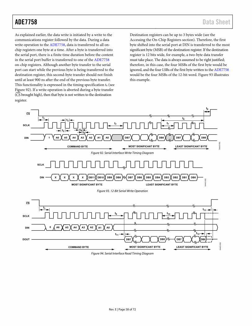
ADE7758 Data Sheet
Rev. E | Page 58 of 72
As explained earlier, the data write is initiated by a write to the communications register followed by the data. During a data write operation to the ADE7758, data is transferred to all on-chip registers one byte at a time. After a byte is transferred into the serial port, there is a finite time duration before the content in the serial port buffer is transferred to one of the ADE7758 on-chip registers. Although another byte transfer to the serial port can start while the previous byte is being transferred to the destination register, this second-byte transfer should not finish until at least 900 ns after the end of the previous byte transfer. This functionality is expressed in the timing specification t6 (see Figure 92). If a write operation is aborted during a byte transfer (CS brought high), then that byte is not written to the destination register.
Destination registers can be up to 3 bytes wide (see the Accessing the On-Chip Registers section). Therefore, the first byte shifted into the serial port at DIN is transferred to the most significant byte (MSB) of the destination register. If the destination register is 12 bits wide, for example, a two-byte data transfer must take place. The data is always assumed to be right justified; therefore, in this case, the four MSBs of the first byte would be ignored, and the four LSBs of the first byte written to the ADE7758 would be the four MSBs of the 12-bit word. Figure 93 illustrates this example.
DIN
SCLK
CS
t2
t3t1
t4 t5
t7
t6
t8
COMMAND BYTE MOST SIGNIFICANT BYTE LEAST SIGNIFICANT BYTE
1 A6 A4A5 A3 A2 A1 A0 DB7 DB0 DB7 DB0
t7
0444
3-09
1
Figure 92. Serial Interface Write Timing Diagram
SCLK
DIN X X X X DB11 DB10 DB9 DB8 DB7 DB6 DB5 DB4 DB3 DB2 DB1 DB0
MOST SIGNIFICANT BYTE LEAST SIGNIFICANT BYTE 0444
3-09
2
Figure 93. 12-Bit Serial Write Operation
SCLK
CS
t1
t10
t13
0 A6 A4A5 A3 A2 A1 A0
DB0DB7 DB0DB7
DIN
DOUT
t11t12
COMMAND BYTE MOST SIGNIFICANT BYTE LEAST SIGNIFICANT BYTE
t9
0444
3-09
3
Figure 94. Serial Interface Read Timing Diagram

Data Sheet ADE7758
Rev. E | Page 59 of 72
SERIAL READ OPERATION During a data read operation from the ADE7758, data is shifted out at the DOUT logic output on the rising edge of SCLK. As was the case with the data write operation, a data read must be preceded with a write to the communications register.
With the ADE7758 in communications mode and CS logic low, an 8-bit write to the communications register takes place first. The MSB of this byte transfer must be a 0, indicating that the next data transfer operation is a read. The seven LSBs of this byte contain the address of the register that is to be read. The
starts shifting out of the register data on the next rising edge of SCLK (see ). At this point, the DOUT logic output switches from a high impedance state and starts driving the data bus. All remaining bits of register data are shifted out on subsequent SCLK rising edges. The serial interface enters communications mode again as soon as the read is completed. The DOUT logic output enters a high impedance state on the falling edge of the last SCLK pulse.
ADE7758Figure 94
The read operation can be aborted by bringing the CS logic input high before the data transfer is completed. The DOUT output enters a high impedance state on the rising edge of CS.
When an ADE7758 register is addressed for a read operation, the entire contents of that register are transferred to the serial port. This allows the ADE7758 to modify its on-chip registers without the risk of corrupting data during a multibyte transfer.
Note that when a read operation follows a write operation, the read command (that is, write to communications register) should not happen for at least 1.1 μs after the end of the write operation. If the read command is sent within 1.1 μs of the write operation, the last byte of the write operation can be lost.
ACCESSING THE ON-CHIP REGISTERS All ADE7758 functionality is accessed via the on-chip registers. Each register is accessed by first writing to the communications register and then transferring the register data. For a full description of the serial interface protocol, see the Serial Interface section.
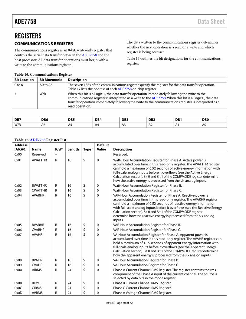
ADE7758 Data Sheet
Rev. E | Page 60 of 72
REGISTERS COMMUNICATIONS REGISTER The communications register is an 8-bit, write-only register that controls the serial data transfer between the ADE7758 and the host processor. All data transfer operations must begin with a write to the communications register.
The data written to the communications register determines whether the next operation is a read or a write and which register is being accessed.
Table 16 outlines the bit designations for the communications register.
Table 16. Communications Register Bit Location Bit Mnemonic Description 0 to 6 A0 to A6 The seven LSBs of the communications register specify the register for the data transfer operation.
Table 17 lists the address of each ADE7758 on-chip register. 7 W/R When this bit is a Logic 1, the data transfer operation immediately following the write to the
communications register is interpreted as a write to the ADE7758. When this bit is a Logic 0, the data transfer operation immediately following the write to the communications register is interpreted as a read operation.
DB7 DB6 DB5 DB4 DB3 DB2 DB1 DB0 W/R A6 A5 A4 A3 A2 A1 A0
Table 17. ADE7758 Register List Address [A6:A0] Name R/W1 Length Type2
Default Value Description
0x00 Reserved – Reserved.
0x01 AWATTHR R 16 S 0 Watt-Hour Accumulation Register for Phase A. Active power is accumulated over time in this read-only register. The AWATTHR register can hold a maximum of 0.52 seconds of active energy information with full-scale analog inputs before it overflows (see the Active Energy Calculation section). Bit 0 and Bit 1 of the COMPMODE register determine how the active energy is processed from the six analog inputs.
0x02 BWATTHR R 16 S 0 Watt-Hour Accumulation Register for Phase B. 0x03 CWATTHR R 16 S 0 Watt-Hour Accumulation Register for Phase C. 0x04 AVARHR R 16 S 0 VAR-Hour Accumulation Register for Phase A. Reactive power is
accumulated over time in this read-only register. The AVARHR register can hold a maximum of 0.52 seconds of reactive energy information with full-scale analog inputs before it overflows (see the Reactive Energy Calculation section). Bit 0 and Bit 1 of the COMPMODE register determine how the reactive energy is processed from the six analog inputs.
0x05 BVARHR R 16 S 0 VAR-Hour Accumulation Register for Phase B. 0x06 CVARHR R 16 S 0 VAR-Hour Accumulation Register for Phase C. 0x07 AVAHR R 16 S 0 VA-Hour Accumulation Register for Phase A. Apparent power is
accumulated over time in this read-only register. The AVAHR register can hold a maximum of 1.15 seconds of apparent energy information with full-scale analog inputs before it overflows (see the Apparent Energy Calculation section). Bit 0 and Bit 1 of the COMPMODE register determine how the apparent energy is processed from the six analog inputs.
0x08 BVAHR R 16 S 0 VA-Hour Accumulation Register for Phase B. 0x09 CVAHR R 16 S 0 VA-Hour Accumulation Register for Phase C. 0x0A AIRMS R 24 S 0 Phase A Current Channel RMS Register. The register contains the rms
component of the Phase A input of the current channel. The source is selected by data bits in the mode register.
0x0B BIRMS R 24 S 0 Phase B Current Channel RMS Register. 0x0C CIRMS R 24 S 0 Phase C Current Channel RMS Register. 0x0D AVRMS R 24 S 0 Phase A Voltage Channel RMS Register.

Data Sheet ADE7758
Rev. E | Page 61 of 72
Address [A6:A0] Name R/W1 Length Type2
Default Value Description
0x0E BVRMS R 24 S 0 Phase B Voltage Channel RMS Register. 0x0F CVRMS R 24 S 0 Phase C Voltage Channel RMS Register. 0x10 FREQ R 12 U 0 Frequency of the Line Input Estimated by the Zero-Crossing Processing.
It can also display the period of the line input. Bit 7 of the LCYCMODE register determines if the reading is frequency or period. Default is frequency. Data Bit 0 and Bit 1 of the MMODE register determine the voltage channel used for the frequency or period calculation.
0x11 TEMP R 8 S 0 Temperature Register. This register contains the result of the latest temperature conversion. Refer to the Temperature Measurement section for details on how to interpret the content of this register.
0x12 WFORM R 24 S 0 Waveform Register. This register contains the digitized waveform of one of the six analog inputs or the digitized power waveform. The source is selected by Data Bit 0 to Bit 4 in the WAVMODE register.
0x13 OPMODE R/W 8 U 4 Operational Mode Register. This register defines the general configuration of the ADE7758 (see Table 18).
0x14 MMODE R/W 8 U 0xFC Measurement Mode Register. This register defines the channel used for period and peak detection measurements (see Table 19).
0x15 WAVMODE R/W 8 U 0 Waveform Mode Register. This register defines the channel and sampling frequency used in the waveform sampling mode (see Table 20).
0x16 COMPMODE R/W 8 U 0x1C Computation Mode Register. This register configures the formula applied for the energy and line active energy measurements (see Table 22).
0x17 LCYCMODE R/W 8 U 0x78 Line Cycle Mode Register. This register configures the line cycle accumulation mode for WATT-HR, VAR-HR, and VA-Hr (see Table 23).
0x18 Mask R/W 24 U 0 IRQ Mask Register. It determines if an interrupt event generates an active-low output at the IRQ pin (see the section). Interrupts
0x19 Status R 24 U 0 IRQ Status Register. This register contains information regarding the source of the interrupts (see the section). ADE7758 Interrupts
0x1A RSTATUS R 24 U 0 IRQ Reset Status Register. Same as the STATUS register, except that its contents are reset to 0 (all flags cleared) after a read operation.
0x1B ZXTOUT R/W 16 U 0xFFFF Zero-Cross Timeout Register. If no zero crossing is detected within the time period specified by this register, the interrupt request line (IRQ) goes active low for the corresponding line voltage. The maximum timeout period is 2.3 seconds (see the section). Zero-Crossing Detection
0x1C LINECYC R/W 16 U 0xFFFF Line Cycle Register. The content of this register sets the number of half-line cycles that the active, reactive, and apparent energies are accumulated for in the line accumulation mode.
0x1D SAGCYC R/W 8 U 0xFF SAG Line Cycle Register. This register specifies the number of consecutive half-line cycles where voltage channel input may fall below a threshold level. This register is common to the three line voltage SAG detection. The detection threshold is specified by the SAGLVL register (see the Line Voltage SAG Detection section).
0x1E SAGLVL R/W 8 U 0 SAG Voltage Level. This register specifies the detection threshold for the SAG event. This register is common to all three phases’ line voltage SAG detections. See the description of the SAGCYC register for details.
0x1F VPINTLVL R/W 8 U 0xFF Voltage Peak Level Interrupt Threshold Register. This register sets the level of the voltage peak detection. Bit 5 to Bit 7 of the MMODE register determine which phases are to be monitored. If the selected voltage phase exceeds this level, the PKV flag in the IRQ status register is set.
0x20 IPINTLVL R/W 8 U 0xFF Current Peak Level Interrupt Threshold Register. This register sets the level of the current peak detection. Bit 5 to Bit 7 of the MMODE register determine which phases are to be monitored. If the selected current phase exceeds this level, the PKI flag in the IRQ status register is set.
0x21 VPEAK R 8 U 0 Voltage Peak Register. This register contains the value of the peak voltage waveform that has occurred within a fixed number of half-line cycles. The number of half-line cycles is set by the LINECYC register.
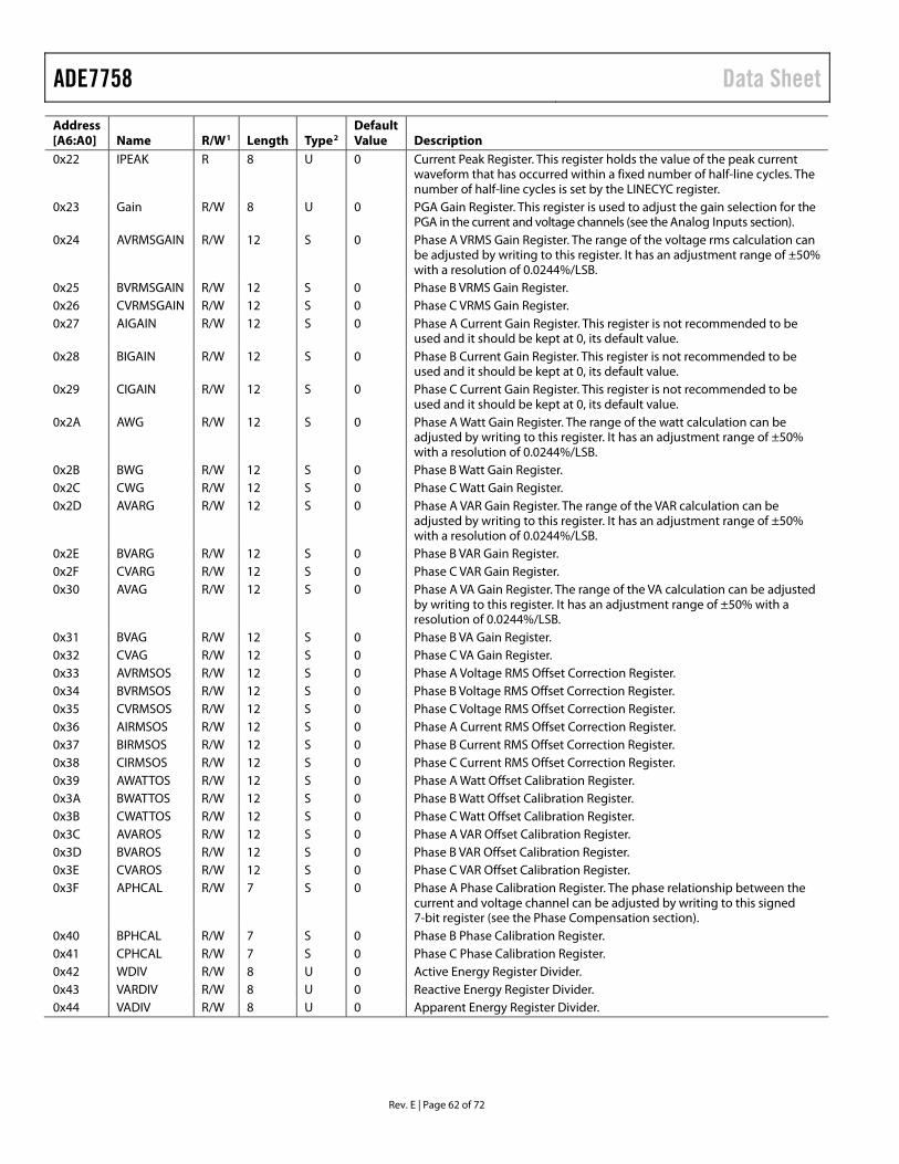
ADE7758 Data Sheet
Rev. E | Page 62 of 72
Address [A6:A0] Name R/W1 Length Type2
Default Value Description
0x22 IPEAK R 8 U 0 Current Peak Register. This register holds the value of the peak current waveform that has occurred within a fixed number of half-line cycles. The number of half-line cycles is set by the LINECYC register.
0x23 Gain R/W 8 U 0 PGA Gain Register. This register is used to adjust the gain selection for the PGA in the current and voltage channels (see the Analog Inputs section).
0x24 AVRMSGAIN R/W 12 S 0 Phase A VRMS Gain Register. The range of the voltage rms calculation can be adjusted by writing to this register. It has an adjustment range of ±50% with a resolution of 0.0244%/LSB.
0x25 BVRMSGAIN R/W 12 S 0 Phase B VRMS Gain Register. 0x26 CVRMSGAIN R/W 12 S 0 Phase C VRMS Gain Register. 0x27 AIGAIN R/W 12 S 0 Phase A Current Gain Register. This register is not recommended to be
used and it should be kept at 0, its default value. 0x28 BIGAIN R/W 12 S 0 Phase B Current Gain Register. This register is not recommended to be
used and it should be kept at 0, its default value. 0x29 CIGAIN R/W 12 S 0 Phase C Current Gain Register. This register is not recommended to be
used and it should be kept at 0, its default value. 0x2A AWG R/W 12 S 0 Phase A Watt Gain Register. The range of the watt calculation can be
adjusted by writing to this register. It has an adjustment range of ±50% with a resolution of 0.0244%/LSB.
0x2B BWG R/W 12 S 0 Phase B Watt Gain Register. 0x2C CWG R/W 12 S 0 Phase C Watt Gain Register. 0x2D AVARG R/W 12 S 0 Phase A VAR Gain Register. The range of the VAR calculation can be
adjusted by writing to this register. It has an adjustment range of ±50% with a resolution of 0.0244%/LSB.
0x2E BVARG R/W 12 S 0 Phase B VAR Gain Register. 0x2F CVARG R/W 12 S 0 Phase C VAR Gain Register. 0x30 AVAG R/W 12 S 0 Phase A VA Gain Register. The range of the VA calculation can be adjusted
by writing to this register. It has an adjustment range of ±50% with a resolution of 0.0244%/LSB.
0x31 BVAG R/W 12 S 0 Phase B VA Gain Register. 0x32 CVAG R/W 12 S 0 Phase C VA Gain Register. 0x33 AVRMSOS R/W 12 S 0 Phase A Voltage RMS Offset Correction Register. 0x34 BVRMSOS R/W 12 S 0 Phase B Voltage RMS Offset Correction Register. 0x35 CVRMSOS R/W 12 S 0 Phase C Voltage RMS Offset Correction Register. 0x36 AIRMSOS R/W 12 S 0 Phase A Current RMS Offset Correction Register. 0x37 BIRMSOS R/W 12 S 0 Phase B Current RMS Offset Correction Register. 0x38 CIRMSOS R/W 12 S 0 Phase C Current RMS Offset Correction Register. 0x39 AWATTOS R/W 12 S 0 Phase A Watt Offset Calibration Register. 0x3A BWATTOS R/W 12 S 0 Phase B Watt Offset Calibration Register. 0x3B CWATTOS R/W 12 S 0 Phase C Watt Offset Calibration Register. 0x3C AVAROS R/W 12 S 0 Phase A VAR Offset Calibration Register. 0x3D BVAROS R/W 12 S 0 Phase B VAR Offset Calibration Register. 0x3E CVAROS R/W 12 S 0 Phase C VAR Offset Calibration Register. 0x3F APHCAL R/W 7 S 0 Phase A Phase Calibration Register. The phase relationship between the
current and voltage channel can be adjusted by writing to this signed 7-bit register (see the Phase Compensation section).
0x40 BPHCAL R/W 7 S 0 Phase B Phase Calibration Register. 0x41 CPHCAL R/W 7 S 0 Phase C Phase Calibration Register. 0x42 WDIV R/W 8 U 0 Active Energy Register Divider. 0x43 VARDIV R/W 8 U 0 Reactive Energy Register Divider. 0x44 VADIV R/W 8 U 0 Apparent Energy Register Divider.
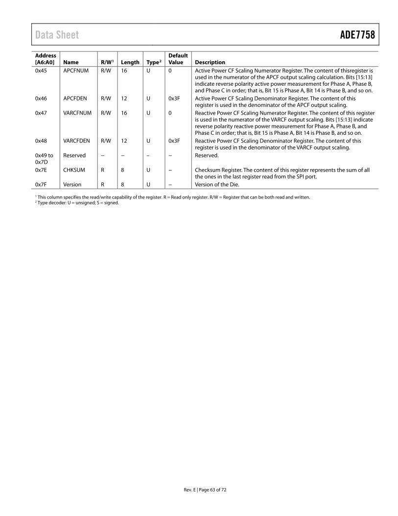
Data Sheet ADE7758
Rev. E | Page 63 of 72
Address [A6:A0] Name R/W1 Length Type2
Default Value Description
0x45 APCFNUM R/W 16 U 0 Active Power CF Scaling Numerator Register. The content of thisregister is used in the numerator of the APCF output scaling calculation. Bits [15:13] indicate reverse polarity active power measurement for Phase A, Phase B, and Phase C in order; that is, Bit 15 is Phase A, Bit 14 is Phase B, and so on.
0x46 APCFDEN R/W 12 U 0x3F Active Power CF Scaling Denominator Register. The content of this register is used in the denominator of the APCF output scaling.
0x47 VARCFNUM R/W 16 U 0 Reactive Power CF Scaling Numerator Register. The content of this register is used in the numerator of the VARCF output scaling. Bits [15:13] indicate reverse polarity reactive power measurement for Phase A, Phase B, and Phase C in order; that is, Bit 15 is Phase A, Bit 14 is Phase B, and so on.
0x48 VARCFDEN R/W 12 U 0x3F Reactive Power CF Scaling Denominator Register. The content of this register is used in the denominator of the VARCF output scaling.
0x49 to 0x7D
Reserved − − – − Reserved.
0x7E CHKSUM R 8 U − Checksum Register. The content of this register represents the sum of all the ones in the last register read from the SPI port.
0x7F Version R 8 U − Version of the Die. 1 This column specifies the read/write capability of the register. R = Read only register. R/W = Register that can be both read and written. 2 Type decoder: U = unsigned; S = signed.
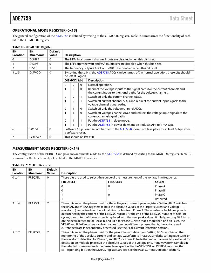
ADE7758 Data Sheet
Rev. E | Page 64 of 72
OPERATIONAL MODE REGISTER (0x13) The general configuration of the ADE7758 is defined by writing to the OPMODE register. Table 18 summarizes the functionality of each bit in the OPMODE register.
Table 18. OPMODE Register Bit Location
Bit Mnemonic
Default Value Description
0 DISHPF 0 The HPFs in all current channel inputs are disabled when this bit is set. 1 DISLPF 0 The LPFs after the watt and VAR multipliers are disabled when this bit is set. 2 DISCF 1 The frequency outputs APCF and VARCF are disabled when this bit is set. 3 to 5 DISMOD 0 By setting these bits, the ADE7758 ADCs can be turned off. In normal operation, these bits should
be left at Logic 0. DISMOD[2:0] Description 0 0 0 Normal operation. 1 0 0 Redirect the voltage inputs to the signal paths for the current channels and
the current inputs to the signal paths for the voltage channels. 0 0 1 Switch off only the current channel ADCs. 1 0 1 Switch off current channel ADCs and redirect the current input signals to the
voltage channel signal paths. 0 1 0 Switch off only the voltage channel ADCs. 1 1 0 Switch off voltage channel ADCs and redirect the voltage input signals to the
current channel signal paths. 0 1 1 Put the ADE7758 in sleep mode. 1 1 1 Put the ADE7758 in power-down mode (reduces AIDD to 1 mA typ). 6 SWRST 0 Software Chip Reset. A data transfer to the ADE7758 should not take place for at least 166 μs after
a software reset. 7 Reserved 0 This should be left at 0.
MEASUREMENT MODE REGISTER (0x14) The configuration of the PERIOD and peak measurements made by the ADE7758 is defined by writing to the MMODE register. Table 19 summarizes the functionality of each bit in the MMODE register.
Table 19. MMODE Register Bit Location
Bit Mnemonic
Default Value Description
0 to 1 FREQSEL 0 These bits are used to select the source of the measurement of the voltage line frequency. FREQSEL1 FREQSEL0 Source 0 0 Phase A 0 1 Phase B 1 0 Phase C 1 1 Reserved 2 to 4 PEAKSEL 7 These bits select the phases used for the voltage and current peak registers. Setting Bit 2 switches
the IPEAK and VPEAK registers to hold the absolute values of the largest current and voltage waveform (over a fixed number of half-line cycles) from Phase A. The number of half-line cycles is determined by the content of the LINECYC register. At the end of the LINECYC number of half-line cycles, the content of the registers is replaced with the new peak values. Similarly, setting Bit 3 turns on the peak detection for Phase B, and Bit 4 for Phase C. Note that if more than one bit is set, the VPEAK and IPEAK registers can hold values from two different phases, that is, the voltage and current peak are independently processed (see the Peak Current Detection section).
5 to 7 PKIRQSEL 7 These bits select the phases used for the peak interrupt detection. Setting Bit 5 switches on the monitoring of the absolute current and voltage waveform to Phase A. Similarly, setting Bit 6 turns on the waveform detection for Phase B, and Bit 7 for Phase C. Note that more than one bit can be set for detection on multiple phases. If the absolute values of the voltage or current waveform samples in the selected phases exceeds the preset level specified in the VPINTLVL or IPINTLVL registers the corresponding bit(s) in the STATUS registers are set (see the Peak Current Detection section).

Data Sheet ADE7758
Rev. E | Page 65 of 72
WAVEFORM MODE REGISTER (0x15) The waveform sampling mode of the ADE7758 is defined by writing to the WAVMODE register. Table 20 summarizes the functionality of each bit in the WAVMODE register.
Table 20. WAVMODE Register Bit Location
Bit Mnemonic
Default Value Description
0 to 1 PHSEL 0 These bits are used to select the phase of the waveform sample.
PHSEL[1:0] Source 0 0 Phase A 0 1 Phase B 1 0 Phase C 1 1 Reserved 2 to 4 WAVSEL 0 These bits are used to select the type of waveform. WAVSEL[2:0] Source 0 0 0 Current 0 0 1 Voltage 0 1 0 Active Power Multiplier Output 0 1 1 Reactive Power Multiplier Output 1 0 0 VA Multiplier Output Others- Reserved 5 to 6 DTRT 0 These bits are used to select the data rate. DTRT[1:0] Update Rate 0 0 26.04 kSPS (CLKIN/3/128) 0 1 13.02 kSPS (CLKIN/3/256) 1 0 6.51 kSPS (CLKIN/3/512) 1 1 3.25 kSPS (CLKIN/3/1024) 7 VACF 0 Setting this bit to Logic 1 switches the VARCF output pin to an output frequency that is
proportional to the total apparent power (VA). In the default state, Logic 0, the VARCF pin outputs a frequency proportional to the total reactive power (VAR).

ADE7758 Data Sheet
Rev. E | Page 66 of 72
COMPUTATIONAL MODE REGISTER (0x16) The computational method of the ADE7758 is defined by writing to the COMPMODE register. Table 21 summarizes the functionality of each bit in the COMPMODE register.
Table 21. COMPMODE Register Bit Location
Bit Mnemonic
Default Value Description
0 to 1 CONSEL 0 These bits are used to select the input to the energy accumulation registers. CONSEL[1:0] = 11 is reserved. IA, IB, and IC are IA, IB, and IC phase shifted by –90°, respectively.
Registers CONSEL[1, 0] = 00 CONSEL[1, 0] = 01 CONSEL[1, 0] = 10 AWATTHR VA × IA VA × (IA – IB) VA × (IA–IB) BWATTHR VB × IB 0 0 CWATTHR VC × IC VC × (IC – IB) VC × IC AVARHR VA × IA VA × (IA – IB) VA × (IA–IB)
BVARHR VB × IB 0 0
CVARHR VC × IC VC × (IC – IB) VC × IC
AVAHR VARMS × IARMS VARMS × IARMS VARMS × ARMS BVAHR VBRMS × IBRMS (VARMS + VCRMS)/2 × IBRMS VARMS × IBRMS CVAHR VCRMS × ICRMS VCRMS × ICRMS VCRMS × ICRMS 2 to 4 TERMSEL 7 These bits are used to select the phases to be included in the APCF and VARCF pulse outputs. Setting
Bit 2 selects Phase A (the inputs to AWATTHR and AVARHR registers) to be included. Bit 3 and Bit 4 are for Phase B and Phase C, respectively. Setting all three bits enables the sum of all three phases to be included in the frequency outputs (see the Active Power Frequency Output and the Reactive Power Frequency Output sections).
5 ABS 0 Setting this bit places the APCF output pin in absolute only mode. Namely, the APCF output frequency is proportional to the sum of the absolute values of the watt-hour accumulation registers (AWATTHR, BWATTHR, and CWATTHR). Note that this bit only affects the APCF pin and has no effect on the content of the corresponding registers.
6 SAVAR 0 Setting this bit places the VARCF output pin in the signed adjusted mode. Namely, the VARCF output frequency is proportional to the sign-adjusted sum of the VAR-hour accumulation registers (AVARHR, BVARHR, and CVARHR). The sign of the VAR is determined from the sign of the watt calculation from the corresponding phase, that is, the sign of the VAR is flipped if the sign of the watt is negative, and if the watt is positive, there is no change to the sign of the VAR. Note that this bit only affects the VARCF pin and has no effect on the content of the corresponding registers.
7 NOLOAD 0 Setting this bit activates the no-load threshold in the ADE7758.

Data Sheet ADE7758
Rev. E | Page 67 of 72
LINE CYCLE ACCUMULATION MODE REGISTER (0x17) The functionalities involved the line-cycle accumulation mode in the ADE7758 are defined by writing to the LCYCMODE register. Table 22 summarizes the functionality of each bit in the LCYCMODE register.
Table 22. LCYCMODE Register Bit Location
Bit Mnemonic
Default Value Description
0 LWATT 0 Setting this bit places the watt-hour accumulation registers (AWATTHR, BWATTHR, and CWATTHR registers) into line-cycle accumulation mode.
1 LVAR 0 Setting this bit places the VAR-hour accumulation registers (AVARHR, BVARHR, and CVARHR registers) into line-cycle accumulation mode.
2 LVA 0 Setting this bit places the VA-hour accumulation registers (AVAHR, BVAHR, and CVAHR registers) into line-cycle accumulation mode.
3 to 5 ZXSEL 7 These bits select the phases used for counting the number of zero crossings in the line-cycle accumulation mode. Bit 3, Bit 4, and Bit 5 select Phase A, Phase B, and Phase C, respectively. More than one phase can be selected for the zero-crossing detection, and the accumulation time is shortened accordingly.
6 RSTREAD 1 Setting this bit enables the read-with-reset for all the WATTHR, VARHR, and VAHR registers for all three phases, that is, a read to those registers resets the registers to 0 after the content of the registers have been read. This bit should be set to Logic 0 when the LWATT, LVAR, or LVA bits are set to Logic 1.
7 FREQSEL 0 Setting this bit causes the FREQ (0x10) register to display the period, instead of the frequency of the line input.

ADE7758 Data Sheet
Rev. E | Page 68 of 72
INTERRUPT MASK REGISTER (0x18) When an interrupt event occurs in the ADE7758, the IRQ logic output goes active low if the mask bit for this event is Logic 1 in the MASK register. The IRQ logic output is reset to its default collector open state when the RSTATUS register is read. describes the function of each bit in the interrupt mask register.
Table 23
Table 23. Function of Each Bit in the Interrupt Mask Register Bit Location
Interrupt Flag
Default Value Description
0 AEHF 0 Enables an interrupt when there is a change in Bit 14 of any one of the three WATTHR registers, that is, the WATTHR register is half full.
1 REHF 0 Enables an interrupt when there is a change in Bit 14 of any one of the three VARHR registers, that is, the VARHR register is half full.
2 VAEHF 0 Enables an interrupt when there is a 0 to 1 transition in the MSB of any one of the three VAHR registers, that is, the VAHR register is half full.
3 SAGA 0 Enables an interrupt when there is a SAG on the line voltage of the Phase A. 4 SAGB 0 Enables an interrupt when there is a SAG on the line voltage of the Phase B. 5 SAGC 0 Enables an interrupt when there is a SAG on the line voltage of the Phase C. 6 ZXTOA 0 Enables an interrupt when there is a zero-crossing timeout detection on Phase A. 7 ZXTOB 0 Enables an interrupt when there is a zero-crossing timeout detection on Phase B. 8 ZXTOC 0 Enables an interrupt when there is a zero-crossing timeout detection on Phase C. 9 ZXA 0 Enables an interrupt when there is a zero crossing in the voltage channel of Phase A (see the
Zero-Crossing Detection section). 10 ZXB 0 Enables an interrupt when there is a zero crossing in the voltage channel of Phase B (see the
Zero-Crossing Detection section). 11 ZXC 0 Enables an interrupt when there is a zero crossing in the voltage channel of Phase C (see the
Zero-Crossing Detection section). 12 LENERGY 0 Enables an interrupt when the energy accumulations over LINECYC are finished. 13 Reserved 0 Reserved. 14 PKV 0 Enables an interrupt when the voltage input selected in the MMODE register is above the value
in the VPINTLVL register. 15 PKI 0 Enables an interrupt when the current input selected in the MMODE register is above the value
in the IPINTLVL register. 16 WFSM 0 Enables an interrupt when data is present in the WAVEMODE register. 17 REVPAP 0 Enables an interrupt when there is a sign change in the watt calculation among any one of the
phases specified by the TERMSEL bits in the COMPMODE register. 18 REVPRP 0 Enables an interrupt when there is a sign change in the VAR calculation among any one of the
phases specified by the TERMSEL bits in the COMPMODE register. 19 SEQERR 0 Enables an interrupt when the zero crossing from Phase A is followed not by the zero crossing
of Phase C but with that of Phase B.
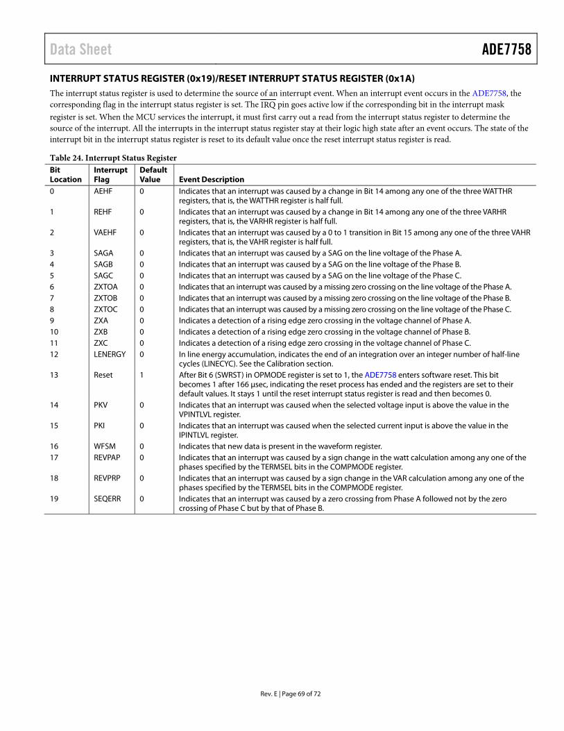
Data Sheet ADE7758
Rev. E | Page 69 of 72
INTERRUPT STATUS REGISTER (0x19)/RESET INTERRUPT STATUS REGISTER (0x1A) The interrupt status register is used to determine the source of an interrupt event. When an interrupt event occurs in the ADE7758, the corresponding flag in the interrupt status register is set. The IRQ pin goes active low if the corresponding bit in the interrupt mask register is set. When the MCU services the interrupt, it must first carry out a read from the interrupt status register to determine the source of the interrupt. All the interrupts in the interrupt status register stay at their logic high state after an event occurs. The state of the interrupt bit in the interrupt status register is reset to its default value once the reset interrupt status register is read.
Table 24. Interrupt Status Register Bit Location
Interrupt Flag
Default Value Event Description
0 AEHF 0 Indicates that an interrupt was caused by a change in Bit 14 among any one of the three WATTHR registers, that is, the WATTHR register is half full.
1 REHF 0 Indicates that an interrupt was caused by a change in Bit 14 among any one of the three VARHR registers, that is, the VARHR register is half full.
2 VAEHF 0 Indicates that an interrupt was caused by a 0 to 1 transition in Bit 15 among any one of the three VAHR registers, that is, the VAHR register is half full.
3 SAGA 0 Indicates that an interrupt was caused by a SAG on the line voltage of the Phase A. 4 SAGB 0 Indicates that an interrupt was caused by a SAG on the line voltage of the Phase B. 5 SAGC 0 Indicates that an interrupt was caused by a SAG on the line voltage of the Phase C. 6 ZXTOA 0 Indicates that an interrupt was caused by a missing zero crossing on the line voltage of the Phase A. 7 ZXTOB 0 Indicates that an interrupt was caused by a missing zero crossing on the line voltage of the Phase B. 8 ZXTOC 0 Indicates that an interrupt was caused by a missing zero crossing on the line voltage of the Phase C. 9 ZXA 0 Indicates a detection of a rising edge zero crossing in the voltage channel of Phase A. 10 ZXB 0 Indicates a detection of a rising edge zero crossing in the voltage channel of Phase B. 11 ZXC 0 Indicates a detection of a rising edge zero crossing in the voltage channel of Phase C. 12 LENERGY 0 In line energy accumulation, indicates the end of an integration over an integer number of half-line
cycles (LINECYC). See the Calibration section. 13 Reset 1 After Bit 6 (SWRST) in OPMODE register is set to 1, the ADE7758 enters software reset. This bit
becomes 1 after 166 μsec, indicating the reset process has ended and the registers are set to their default values. It stays 1 until the reset interrupt status register is read and then becomes 0.
14 PKV 0 Indicates that an interrupt was caused when the selected voltage input is above the value in the VPINTLVL register.
15 PKI 0 Indicates that an interrupt was caused when the selected current input is above the value in the IPINTLVL register.
16 WFSM 0 Indicates that new data is present in the waveform register. 17 REVPAP 0 Indicates that an interrupt was caused by a sign change in the watt calculation among any one of the
phases specified by the TERMSEL bits in the COMPMODE register. 18 REVPRP 0 Indicates that an interrupt was caused by a sign change in the VAR calculation among any one of the
phases specified by the TERMSEL bits in the COMPMODE register. 19 SEQERR 0 Indicates that an interrupt was caused by a zero crossing from Phase A followed not by the zero
crossing of Phase C but by that of Phase B.
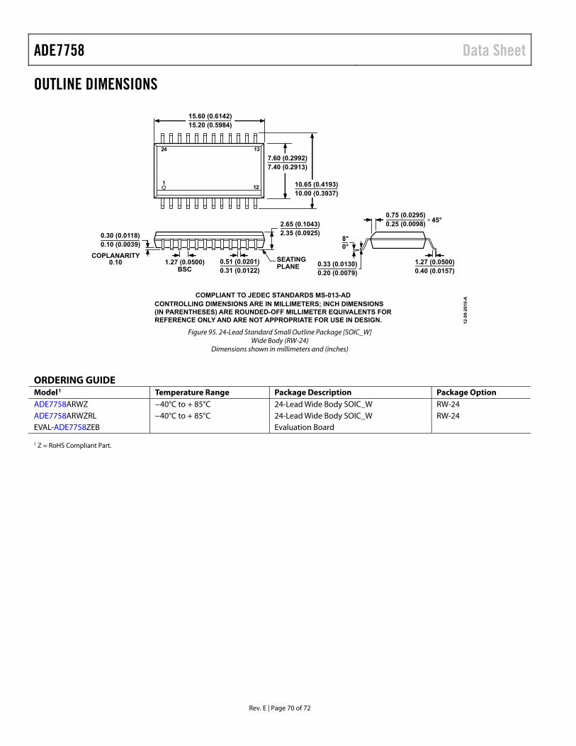
ADE7758 Data Sheet
Rev. E | Page 70 of 72
OUTLINE DIMENSIONS
COMPLIANT TO JEDEC STANDARDS MS-013-ADCONTROLLING DIMENSIONS ARE IN MILLIMETERS; INCH DIMENSIONS(IN PARENTHESES) ARE ROUNDED-OFF MILLIMETER EQUIVALENTS FORREFERENCE ONLY AND ARE NOT APPROPRIATE FOR USE IN DESIGN.
15.60 (0.6142)15.20 (0.5984)
0.30 (0.0118)0.10 (0.0039)
2.65 (0.1043)2.35 (0.0925)
10.65 (0.4193)10.00 (0.3937)
7.60 (0.2992)7.40 (0.2913)
0.75 (0.0295)0.25 (0.0098) 45°
1.27 (0.0500)0.40 (0.0157)
COPLANARITY0.10 0.33 (0.0130)
0.20 (0.0079)0.51 (0.0201)0.31 (0.0122)
SEATINGPLANE
8°0°
24 13
121
1.27 (0.0500)BSC
12-0
9-20
10-A
Figure 95. 24-Lead Standard Small Outline Package [SOIC_W]
Wide Body (RW-24) Dimensions shown in millimeters and (inches)
ORDERING GUIDE Model1 Temperature Range Package Description Package Option ADE7758ARWZ −40°C to + 85°C 24-Lead Wide Body SOIC_W RW-24 ADE7758ARWZRL −40°C to + 85°C 24-Lead Wide Body SOIC_W RW-24 EVAL-ADE7758ZEB Evaluation Board 1 Z = RoHS Compliant Part.

Data Sheet ADE7758
Rev. E | Page 71 of 72
NOTES

ADE7758 Data Sheet
Rev. E | Page 72 of 72
NOTES
©2004–2011 Analog Devices, Inc. All rights reserved. Trademarks and registered trademarks are the property of their respective owners. D04443-0-10/11(E)