Embed Size (px)
Citation preview

Evaluation Board for AD5360/AD5361/AD5362/AD5363
Preliminary Technical Data EVAL-AD5360/1/2/3EBZ
Rev. PrC Information furnished by Analog Devices is believed to be accurate and reliable. However, no responsibility is assumed by Analog Devices for its use, nor for any infringements of patents or other rights of third parties that may result from its use. Specifications subject to change without notice. No license is granted by implication or otherwise under any patent or patent rights of Analog Devices. Trademarks and registered trademarks are the property of their respective companies.
One Technology Way, P.O. Box 9106, Norwood, MA 02062-9106, U.S.A. Tel: 781.329.4700 www.analog.com Fax: 781.326.8703 © 2008 Analog Devices, Inc. All rights reserved.
FEATURES
Full-Featured Evaluation Board for the AD5360/AD5361/AD5362/AD5363 USB Interface PC Software for Register Programming Various Reference Voltages Available Stand-Alone Operation
INTRODUCTION
This Technical Note describes the operation and functionality of the Evaluation Board for the AD5360, AD5361, AD5362 and AD5363. As these 4 parts are pin compatible the same evaluation board is used for all. AD536x will be used throughout this technical note to refer to the actual multi-channel DAC used on the board. This note should be used in conjunction with the data sheet of the appropriate DAC. The evaluation board allows the functionality and performance of the AD536x to be evaluated easily. The evaluation board can be used as a stand alone board with control coming from an external DSP or micro-controller or it can be connected to a PC. Software is provided which can be used to program the registers of the AD536x. Control of the AD536x is achieved via a USB interface
FUNCTIONAL BLOCK DIAGRAM
USBINTERFACE
AD536x
DINSDOSCLKSYNCLDACCLR
RESET
BU
FFER
LK1(USB Used)
HEADER
VOUT0VOUT1
::::
VOUTn
HEA
DER
VREF0VREF1
5V
3V
EXT VREF
VREFSELECTION
EVAL-AD5360_1_2_3EB
DVC
CD
GN
DVD
DAG
ND
VSS
Figure 1. Functional Block Diagram

EVAL-AD5360/1/2/3EBZ Preliminary Technical Data
Rev. PrC | Page 2 of 12
TABLE OF CONTENTS General Description ......................................................................... 3
Functionality Overview ................................................................... 3
Power Supplies .................................................................................. 3
Reference Selection........................................................................... 3
DAC Outputs..................................................................................... 3
Using The USB Interface ..................................................................3
Stand-Alone Operation ....................................................................3
Using the USB Software....................................................................4
Schematics ..........................................................................................9
REVISION HISTORY

Preliminary Technical Data EVAL-AD5360/1/2/3EBZ
Rev. PrC | Page 3 of 12
GENERAL DESCRIPTION FUNCTIONALITY OVERVIEW The evaluation board for the AD536x is designed to allow the user to fully evaluate all the functions and performance of the AD536x prior to designing it into a system. The evaluation board can be used in a stand-alone mode with the control signals being provided through the 20 pin header J3 or it can be connected to a PC using the USB cable supplied with the evaluation board kit. Software is provided which allows the user to program the various registers of the AD536x with ease. The software operation is described later in this document.
POWER SUPPLIES The evaluation board requires a +5V supply for DVCC. The VDD and VSS supplies can be any value within the power supply limits as specified in the AD536x data sheet. Power supply connections are made to the screw terminals of J2. The USB interface, if used, gets its power supply from the USB port of the PC. This power supply is not used by the AD536x or any of its associated circuitry. When connecting the power supply leads it is recommended that the supplies are turned off and that the ground leads are connected first.
REFERENCE SELECTION The evaluation board includes two voltage references ICs, the ADR435 and ADR423 which are 5V and 3V references respectively. An SMB connector is provided to allow an external voltage to be connected for use as a reference. Link LK4 is used to select which reference source is used by the AD536x as shown in Table 1.
Table 1. Reference Selection using LK4 LK4 Position
Description
A The reference voltage is 3V B The reference voltage is 5V (default) C The voltage on the SMB connector, EXT_REF, is
used as the reference voltage
By default the voltage reference pins of the AD536x, VREF0 and VREF1, both use the same reference, i.e. that selected by LK4. If it is required that the reference pins should use different voltage references this can be achieved by removing the 0Ω resistor associated with each VREF pin. The required reference can then be connected to the testpoint associated with the VREF pin. Table 2 shows the 0Ω resistor and testpoint associated with each VREF pin.
Table 2. 0Ω Resistor and Testpoints for VREF pins VREF Resistor Testpoint VREF0 R16 T25 VREF1 R17 T26
DAC OUTPUTS The DAC outputs are available on the 50 pin header J4. The first 16 pins are the 16 VOUT pins for the AD5360 and AD5361 devices. When the AD5362 or AD5363 is used the outputs are available on the pins indicated in Table 3.
Table 3. DAC Output Pins for AD5362 and AD5363 VOUT Pin Pin VOUT VOUT0 1 2 VOUT1 VOUT2 3 4 VOUT3 VOUT4 9 10 VOUT5 VOUT6 11 12 VOUT7
USING THE USB INTERFACE The software provided with the evaluation board kit allows the user to program the registers of the AD536x via the USB interface. It is important that the software supplied is installed on the PC before the board is connected. See the Using the USB Software section for more information. The USB circuitry gets its power from the USB port of the PC and will generate the required interface signals, RESET, CLR, SYNC, SCLK etc. to control the AD536x. To use the interface LK1, LK3 and LK8 should be in place. The function of these links is described in Table 5. LK2 should be in position A to select the binary numeric format which is required for USB operation.
STAND-ALONE OPERATION The evaluation board can be used as a stand-alone device if required. This has the advantage that it lets the user to connect the interface pins of the AD536x to their own DSP or micro-controller thus allowing them to write code to operate the AD536x as their application requires. To use the board in stand-alone mode the connection to the USB interface must be removed. This is achieved by removing LK1, which will three-state the connections to CLR, LDAC, SYNC, SCLK and DIN. LK3 should be removed to isolate the RESET pin from the USB interface and the push-button. The interface signals required to control the AD536x can then be provided through the 20 pin header J3. The pinout of J3 is shown in Table 4
Table 4. J3 Header Pinout Pin Signal Pin Signal
1 DIN 8 LDAC
2 NC 10 CLR
3 SCLK 12 BUSY
4 NC 14 RESET
5 NC 16 NC 6 SYNC 18 NC
7,9,11,13, 15,17,19,20
DGND
EVAL-AD5360/1/2/3EBZ Preliminary Technical Data
Rev. PrC | Page 4 of 12
Table 5. Summary of Link Positions Link Description
LK1 Determines if the USB interface is to be used If this link is inserted the USB interface will generate the signals required to control the AD536x If this link is removed the USB interface is not used and header J3 must be used to provde signals to the AD536x
LK2 Selects the numberic format for the DAC codes If this link is in position A then Binary Format is used. This option should be selected if the PC software is used If this link is in position B then 2s Complement Format is used
LK3 Selects Source of the RESET signal If this link is inserted the RESETsignal comes from either the RESET push-button being pressed or a RESET signal being issued by the USB interface If this link is removed the RESET signal must come for the header J3
LK4 Selects the Reference Source If this link is in position A the 3V reference is selected If this link is in position B the 5V reference is selected If this link is in position C the voltage on SMB connector EXT_REF is selected
LK8 Selects the Source of the CLR signal If this link is inserted the CLR signal comes from the USB interface If this link is removed the CLR signal must come for the header J3
USING THE USB SOFTWARE The evaluation board kit comes supplied with a CD containing PC software allowing the user to control the evaluation board via the USB interface. The software must be installed before the evaluation board is connected to the USB port. The software installation program usually runs automatically when the CD is inserted in the drive but if this doesn’t happen the user should double-click on the SETUP.EXE file in the root directory of the CD. The software will be installed and shortcuts will be placed on the Start Menu in a folder called Analog Devices. When the software has been installed the evaluation board can be connected to the USB port.
When the software is started the user is presented with a selection box. The selection box presents a choice of all the high channel count DACs in the AD536x and AD537x family. The user should click the button appropriate to the board being used.
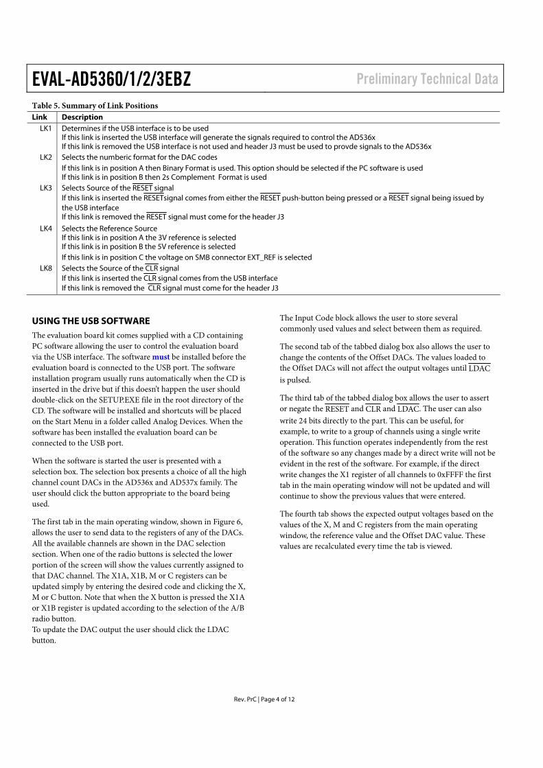
The first tab in the main operating window, shown in Figure 6, allows the user to send data to the registers of any of the DACs. All the available channels are shown in the DAC selection section. When one of the radio buttons is selected the lower portion of the screen will show the values currently assigned to that DAC channel. The X1A, X1B, M or C registers can be updated simply by entering the desired code and clicking the X, M or C button. Note that when the X button is pressed the X1A or X1B register is updated according to the selection of the A/B radio button. To update the DAC output the user should click the LDAC button.
The Input Code block allows the user to store several commonly used values and select between them as required.
The second tab of the tabbed dialog box also allows the user to change the contents of the Offset DACs. The values loaded to the Offset DACs will not affect the output voltages until LDAC is pulsed.
The third tab of the tabbed dialog box allows the user to assert or negate the RESET and CLR and LDAC. The user can also write 24 bits directly to the part. This can be useful, for example, to write to a group of channels using a single write operation. This function operates independently from the rest of the software so any changes made by a direct write will not be evident in the rest of the software. For example, if the direct write changes the X1 register of all channels to 0xFFFF the first tab in the main operating window will not be updated and will continue to show the previous values that were entered.
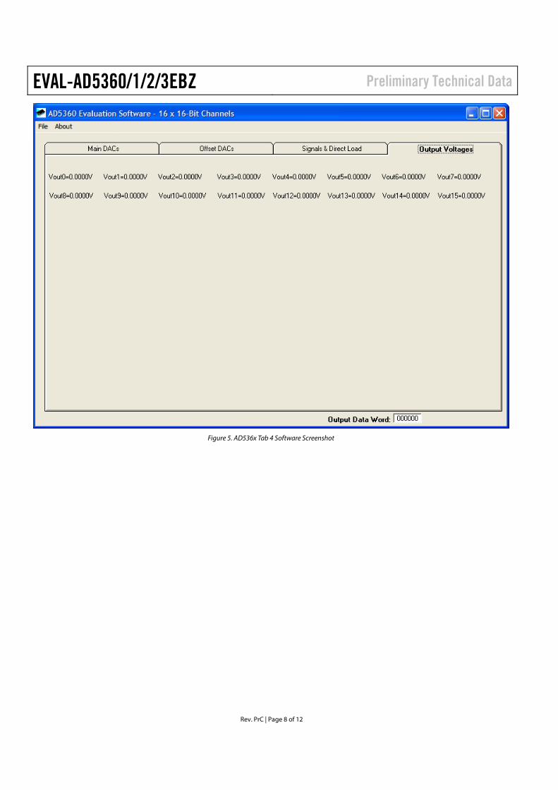
The fourth tab shows the expected output voltages based on the values of the X, M and C registers from the main operating window, the reference value and the Offset DAC value. These values are recalculated every time the tab is viewed.
Preliminary Technical Data EVAL-AD5360/1/2/3EBZ
Rev. PrC | Page 5 of 12
Figure 2. AD536x Tab 1 Software Screenshot

EVAL-AD5360/1/2/3EBZ Preliminary Technical Data
Rev. PrC | Page 6 of 12
Figure 3. AD536x Tab 2 Software Screenshot

Preliminary Technical Data EVAL-AD5360/1/2/3EBZ
Rev. PrC | Page 7 of 12
Figure 4. AD536x Tab 3 Software Screenshot
EVAL-AD5360/1/2/3EBZ Preliminary Technical Data
Rev. PrC | Page 8 of 12
Figure 5. AD536x Tab 4 Software Screenshot

Preliminary Technical Data EVAL-AD5360/1/2/3EBZ
Rev. PrC | Page 9 of 12
SCHEMATICS
Figure 6. AD536x Schematic (1 of 2)

EVAL-AD5360/1/2/3EBZ Preliminary Technical Data
Rev. PrC | Page 10 of 12
Figure 7. AD536x Schematic (2 of 2)
Figure 8. AD536x Component Side Silkscreen

Preliminary Technical Data EVAL-AD5360/1/2/3EBZ
Rev. PrC | Page 11 of 12
Table 6. Bill Of Materials Name Part Type Value Part Description Stock Code1 U1 AD536X 8/16-Channel 16/14-Bit DAC U2 ADP3303-3.3 Precision Low Dropout Voltage
Regulator ADP3303AR-3.3
U8 ADR423 3V Reference ADR423AR U5 ADR435 5V Reference ADR435AR U3 24LC64 64K I2C Serial EEPROM Digikey 24LC64-I/SN-ND U4 74HC245 Bus Transciever Digikey 296-8279-1-ND U7 CY7C68013-CSP USB Microcontroller CY7C68013-56LFC J4 HEADER50 50 Pin (2x25) 0.1" Pitch Header FEC 148-535
J2 CON\POWER5 5 Pin Termical Block FEC 151-785 & 151-786 S1 SW-PUSH Push Button Switch (sealed 6mm x
6mm) FEC 177-807
C3, C11, C25, C27, C37, C39
CAP+ 10μF 10V SMD Tantalum Capacitor FEC 197-130
C21, C23, C29, C31, C33, C42
CAP+ 10μF 25V SMD Tantalum Capacitor FEC 197-518
C17 CAP 1μF 10V DC Y5V Ceramic Capacitor FEC 318-8840 D1 LED Green Light Emitting Diode FEC 359-9681 EXT_REF SMB 50r Straight SMB Jack FEC 365 1228 J1 USB-MINI-B USB Mini-B Connector (usb-otg) FEC 476-8309
(Digikey WM2499CT-ND) C4 CAP+ 2.2μF 10V SMD Tantalum Capacitor FEC 498-646 LK1, LK3, LK8 JUMPER 2 Pin (0.1" Pitch) Header & Shorting
Shunt FEC 511-705 & 150-411
LK2 JUMPER2\SIP3 3 Pin (0.1" Pitch) Header & Shorting Shunt
FEC 511-717 & 150-411
LK4 JUMPER-3 6 Pin (3x2) 0.1" Header & Shorting Block
FEC 511-780 & 150-411
J3 HEADER20 20 Pin (2x10) 0.1" Pitch Header FEC 511-833 Y1 XTAL-CM309S 24 MHz Plastic SMD Crystal FEC 569-872 U6 NC7S08 Tinylogic AND Gate FEC 685-926 C1, C2 CAP 22pF 50V NPO SMD Ceramic Capacitor FEC 722-005 R1, R16, R17 RES 0Ω SMD Resistor FEC 772-227
T1, T3, T11, T12, T13, T14, T15, T16, T17, T18
TESTPOINT Black Testpoint FEC 873-1128
T2, T4, T5, T6, T7, T8, T9, T10, T19, T20, T21, T22, T23, T24, T25, T26, T27
TESTPOINT Red Testpoint FEC 873-1144
Name Part Type Value Part Description Stock Code
V0-V15 TESTPOINT Red Testpoint FEC 873-1144

EVAL-AD5360/1/2/3EBZ Preliminary Technical Data
Rev. PrC | Page 12 of 12 EB07535-0-5/08(PrC)
C5, C6, C7, C8, C9, C10, C12, C13, C14, C15, C16, C18, C19, C20, C22, C24, C26, C28, C30, C32, C36, C38, C40, C41, C43, C44
CAP 0.1μF 50V X7R Multilayer Ceramic Capacitor
FEC 882-0023
R7 RES 1kΩ SMD Resistor FEC 911-239 R2 RES 10kΩ SMD Resistor FEC 911-355 R4 RES 10kΩ SMD Resistor FEC 911-355 R5 RES 10kΩ SMD Resistor FEC 911-355
R3, R6, R8, R9, R13, R14, R15, R18
RES 100kΩ SMD Resistor FEC 911-471
1 FEC = www.farnell.com, Digikey = www.digikey.com