Embed Size (px)
Citation preview
Ahmer Syed
VP – Mechanical Engineering
Emerging IC Packaging TechnologiesEmerging IC Packaging Technologies
Where Are We Going …Where Are We Going …
Enabling a
Microelectronic
World®
December 2012
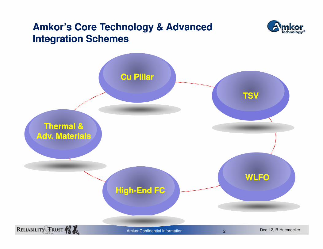
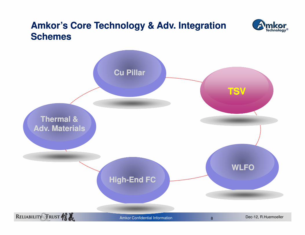
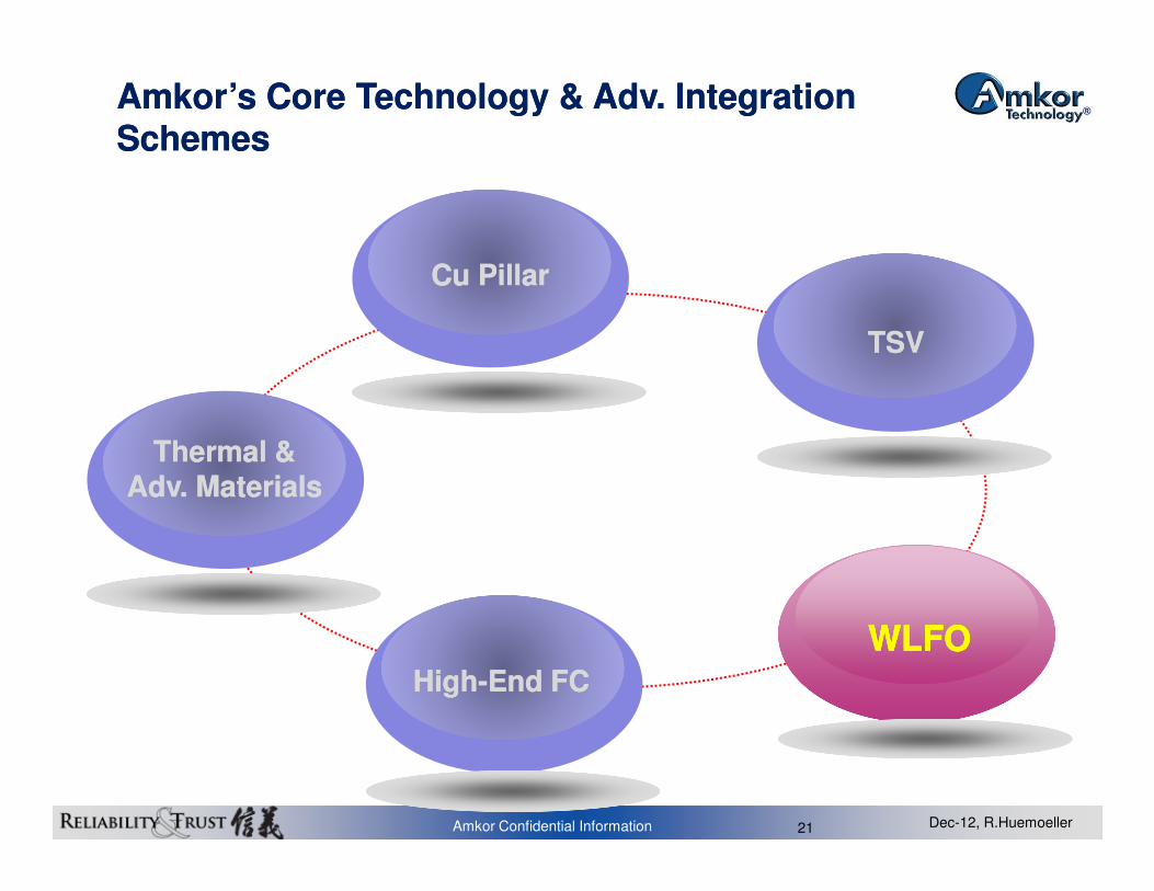
Amkor’s Core Technology & Advanced Amkor’s Core Technology & Advanced Integration SchemesIntegration Schemes
Thermal &Thermal &
Cu PillarCu Pillar
TSVTSV
Amkor Confidential Information Dec-12, R.Huemoeller2
WLFOWLFO
Thermal &Thermal &Adv. MaterialsAdv. Materials
HighHigh--End FCEnd FC
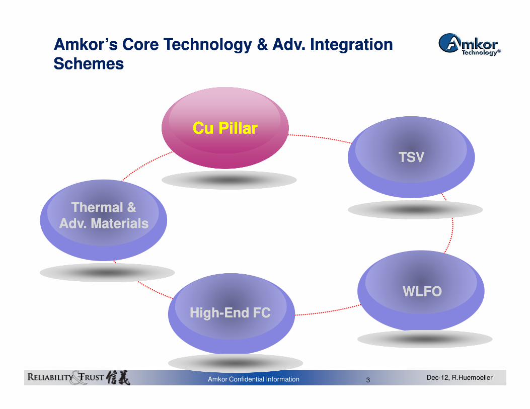
Amkor’s Core Technology & Adv. Integration Amkor’s Core Technology & Adv. Integration SchemesSchemes
Thermal &Thermal &
Cu PillarCu PillarCu PillarCu Pillar
TSVTSV
Amkor Confidential Information Dec-12, R.Huemoeller3
WLFOWLFO
Thermal &Thermal &Adv. MaterialsAdv. Materials
HighHigh--End FCEnd FC
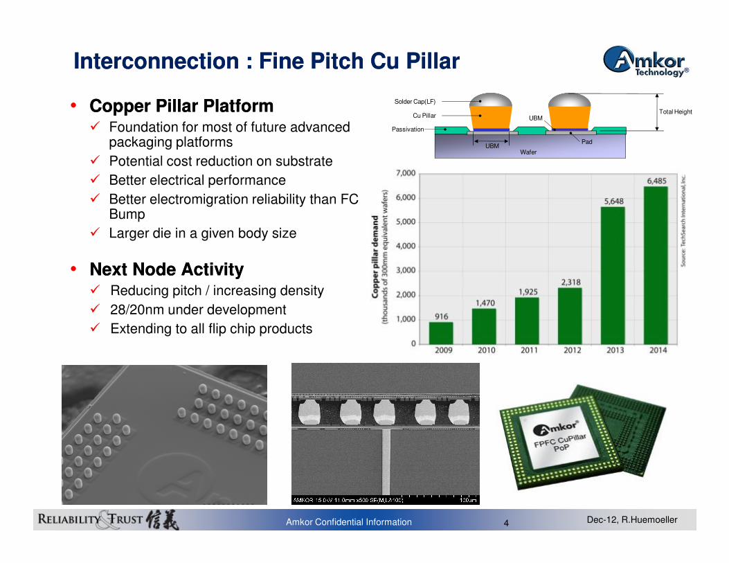
Interconnection : Fine Pitch Cu PillarInterconnection : Fine Pitch Cu Pillar
•• Copper Copper Pillar PlatformPillar Platform� Foundation for most of future advanced
packaging platforms
� Potential cost reduction on substrate
� Better electrical performance
� Better electromigration reliability than FC Bump
� Larger die in a given body size
•• Next Node ActivityNext Node Activity
Wafer
Passivation
Pad
UBMTotal Height
UBM
Cu Pillar
Solder Cap(LF)
Amkor Confidential Information Dec-12, R.Huemoeller4
� Reducing pitch / increasing density
� 28/20nm under development
� Extending to all flip chip products
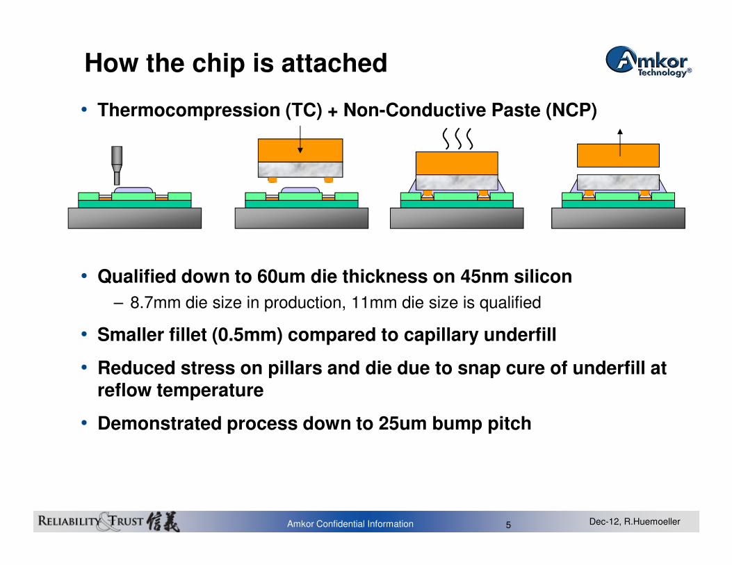
• Thermocompression (TC) + Non-Conductive Paste (NCP)
• Qualified down to 60um die thickness on 45nm silicon
How the chip is attached
Amkor Confidential Information Dec-12, R.Huemoeller5
• Qualified down to 60um die thickness on 45nm silicon
– 8.7mm die size in production, 11mm die size is qualified
• Smaller fillet (0.5mm) compared to capillary underfill
• Reduced stress on pillars and die due to snap cure of underfill at reflow temperature
• Demonstrated process down to 25um bump pitch
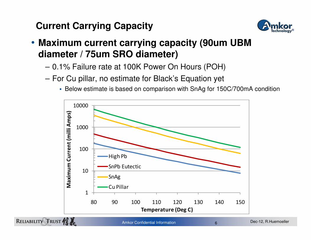
Current Carrying Capacity
• Maximum current carrying capacity (90um UBM diameter / 75um SRO diameter)
– 0.1% Failure rate at 100K Power On Hours (POH)
– For Cu pillar, no estimate for Black’s Equation yet
� Below estimate is based on comparison with SnAg for 150C/700mA condition
10000
Ma
xim
um
Cu
rre
nt
(mil
li A
mp
s)
Amkor Confidential Information Dec-12, R.Huemoeller6
1
10
100
1000
80 90 100 110 120 130 140 150
Ma
xim
um
Cu
rre
nt
(mil
li A
mp
s)
Temperature (Deg C)
High Pb
SnPb Eutectic
SnAg
Cu Pillar
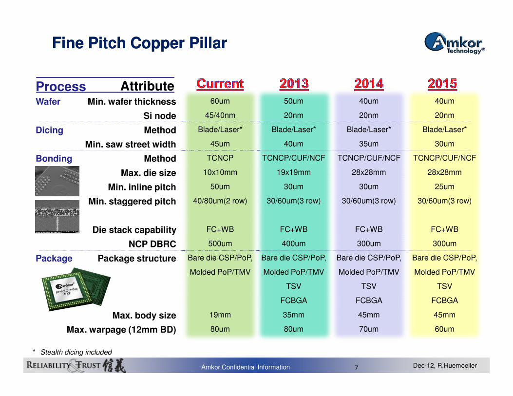
Fine Pitch Copper PillarFine Pitch Copper Pillar
AttributeMin. wafer thickness
Si node
Method
Min. saw street width
Method
Max. die size
Min. inline pitch
Min. staggered pitch
ProcessWafer
Dicing
Bonding
60um
45/40nm
Blade/Laser*
45um
TCNCP
10x10mm
50um
40/80um(2 row)
50um
20nm
Blade/Laser*
40um
TCNCP/CUF/NCF
19x19mm
30um
30/60um(3 row)
40um
20nm
Blade/Laser*
35um
TCNCP/CUF/NCF
28x28mm
30um
30/60um(3 row)
40um
20nm
Blade/Laser*
30um
TCNCP/CUF/NCF
28x28mm
25um
30/60um(3 row)
Amkor Confidential Information Dec-12, R.Huemoeller7
* Stealth dicing included
Min. staggered pitch
Die stack capability
NCP DBRC
Package structure
Max. body size
Max. warpage (12mm BD)
Package
40/80um(2 row)
FC+WB
500um
Bare die CSP/PoP,
Molded PoP/TMV
19mm
80um
30/60um(3 row)
FC+WB
400um
Bare die CSP/PoP,
Molded PoP/TMV
TSV
FCBGA
35mm
80um
30/60um(3 row)
FC+WB
300um
Bare die CSP/PoP,
Molded PoP/TMV
TSV
FCBGA
45mm
70um
30/60um(3 row)
FC+WB
300um
Bare die CSP/PoP,
Molded PoP/TMV
TSV
FCBGA
45mm
60um
Amkor’s Core Technology & Adv. Integration Amkor’s Core Technology & Adv. Integration SchemesSchemes
Thermal &Thermal &
Cu PillarCu Pillar
TSVTSVTSVTSV
Amkor Confidential Information Dec-12, R.Huemoeller8
WLFOWLFO
Thermal &Thermal &Adv. MaterialsAdv. Materials
HighHigh--End FCEnd FC
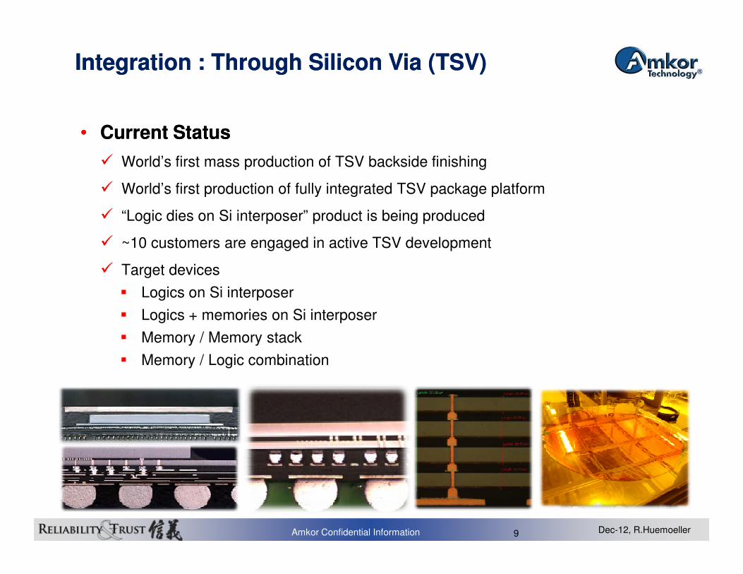
Integration : Through Silicon Via (TSV)Integration : Through Silicon Via (TSV)
•• Current StatusCurrent Status
� World’s first mass production of TSV backside finishing
� World’s first production of fully integrated TSV package platform
� “Logic dies on Si interposer” product is being produced
� ~10 customers are engaged in active TSV development
� Target devices
� Logics on Si interposer
Amkor Confidential Information Dec-12, R.Huemoeller9
� Logics on Si interposer
� Logics + memories on Si interposer
� Memory / Memory stack
� Memory / Logic combination
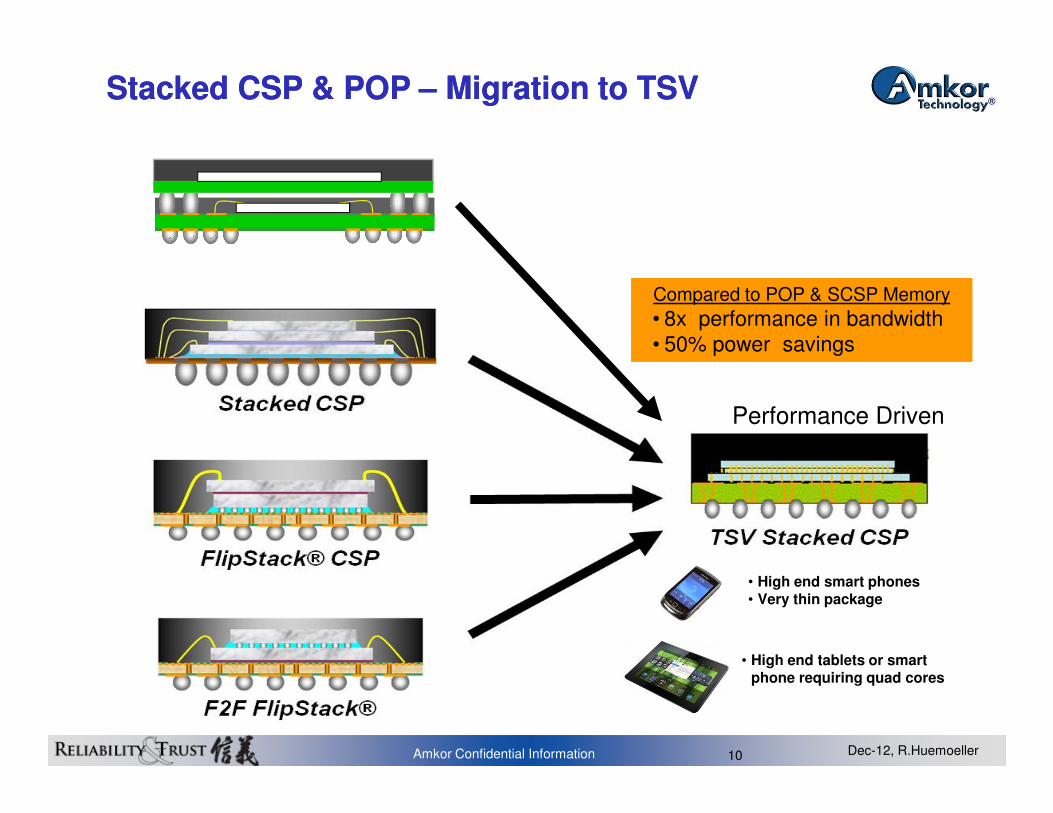
Stacked CSP & POP Stacked CSP & POP –– MigratioMigration to TSVn to TSV
Performance Driven
Compared to POP & SCSP Memory
• 8x performance in bandwidth
• 50% power savings
Amkor Confidential Information Dec-12, R.Huemoeller10
Performance Driven
• High end smart phones• Very thin package
• High end tablets or smart phone requiring quad cores
Logic Die
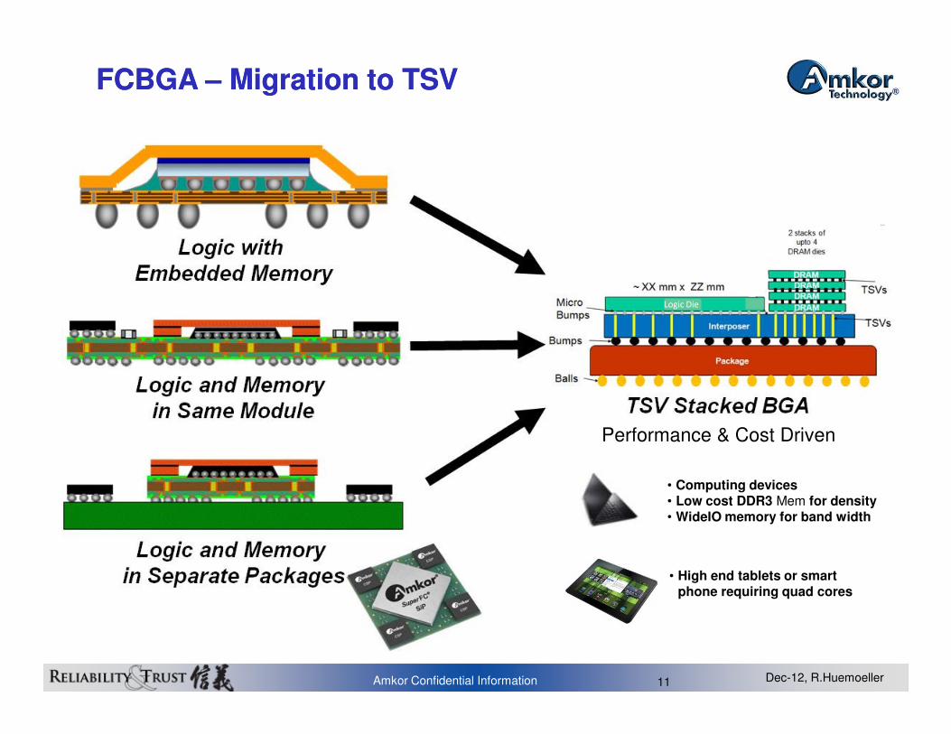
FCBGA FCBGA –– MigratioMigration to TSVn to TSV
Amkor Confidential Information Dec-12, R.Huemoeller11
Performance & Cost Driven
• High end tablets or smart phone requiring quad cores
• Computing devices• Low cost DDR3 Mem for density• WideIO memory for band width
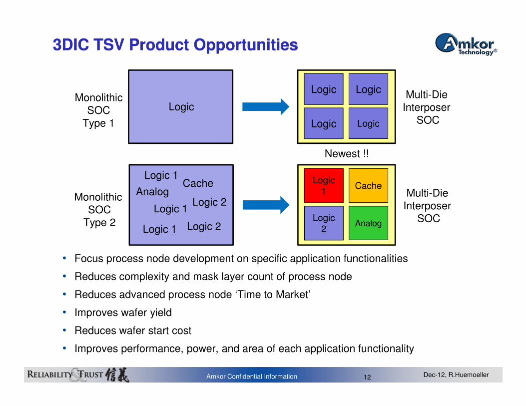
3DIC TSV Product Opportunities3DIC TSV Product Opportunities
Logic 1
Logic 1Logic 2
CacheAnalog
Logic1
Cache
Monolithic
Newest !!
Multi-Die
Interposer
Multi-Die
Interposer
SOC
Logic
Logic
Logic
Logic
Logic
Monolithic
SOC
Type 1
Amkor Confidential Information Dec-12, R.Huemoeller12
• Focus process node development on specific application functionalities
• Reduces complexity and mask layer count of process node
• Reduces advanced process node ‘Time to Market’
• Improves wafer yield
• Reduces wafer start cost
• Improves performance, power, and area of each application functionality
Logic 1
Logic 1
Logic 2
Logic 2Logic
2Analog
SOC
Type 2
Interposer
SOC
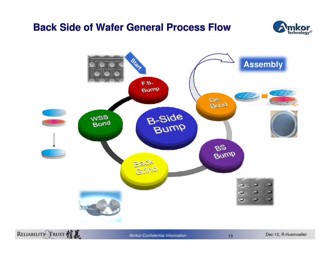
Assembly Process Flow (FOL)Back Side of Wafer General Process FlowBack Side of Wafer General Process Flow
Assembly
Amkor Confidential Information Dec-12, R.Huemoeller13
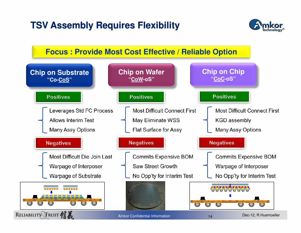
Focus : Provide Most Cost Effective / Reliable Option
Chip on Chip“CoC-oS”
Chip on Wafer“CoW-oS”
Chip on Substrate“Co-CoS”
TSV Assembly Requires FlexibilityTSV Assembly Requires Flexibility
Amkor Confidential Information Dec-12, R.Huemoeller14
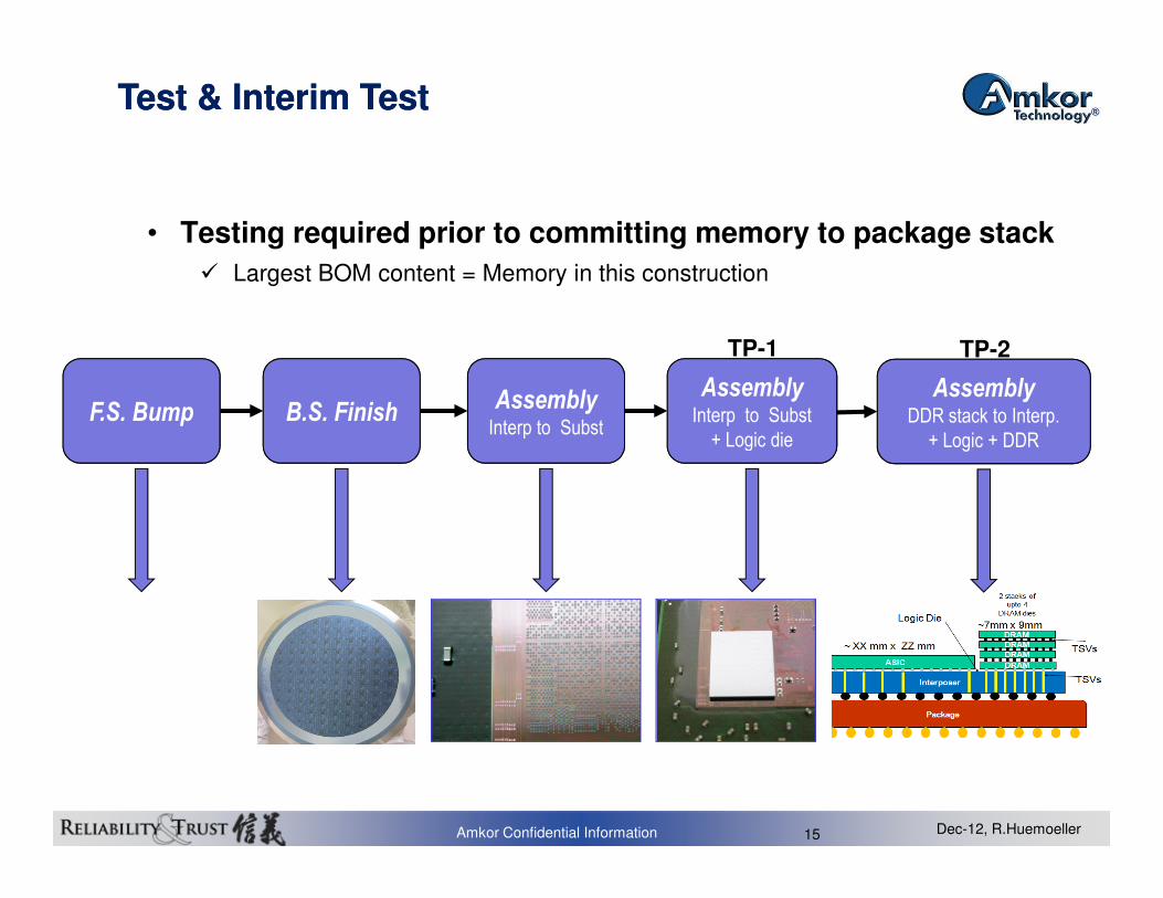
• Testing required prior to committing memory to package stack
� Largest BOM content = Memory in this construction
B.S. FinishB.S. Finish AssemblyInterp to Subst
AssemblyInterp to Subst
AssemblyInterp to Subst
+ Logic die
AssemblyInterp to Subst
+ Logic die
AssemblyDDR stack to Interp.
+ Logic + DDR
AssemblyDDR stack to Interp.
+ Logic + DDR
F.S. BumpF.S. Bump
TP-1 TP-2
Test & Interim TestTest & Interim Test
Amkor Confidential Information Dec-12, R.Huemoeller15
+ Logic die+ Logic die + Logic + DDR+ Logic + DDR
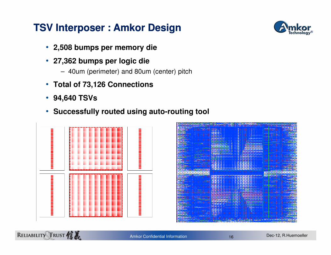
• 2,508 bumps per memory die
• 27,362 bumps per logic die
– 40um (perimeter) and 80um (center) pitch
• Total of 73,126 Connections
• 94,640 TSVs
• Successfully routed using auto-routing tool
TSV Interposer : Amkor DesignTSV Interposer : Amkor Design
Amkor Confidential Information Dec-12, R.Huemoeller16
Silicon InterposersSilicon Interposers
• Sources
─ Amkor is engaged with three sources who are delivering silicon interposers
─ An additional two sources are under collaboration discussion
• Logistics
– Amkor receiving full thickness wafers in from two primary sources
• Amkor bumps front side and finishes backside of wafer
Amkor Confidential Information Dec-12, R.Huemoeller17
• Amkor bumps front side and finishes backside of wafer
• Activity
─ Multiple programs in progress
– Most targeting 100µm as finished thickness ; some thinner to 50µm
– Several with backside RDL requirements
– A few with passive components on top side of interposer
– Both heterogeneous and homogeneous die layouts on interposer
MemoryMemory
• Sources
─ Customer choosing memory supplier
─ Receiving memory from 2 different sources today
• Logistics
─ Amkor working with customers to finalize model
• Plan is receive memory as ‘KGM’ on tape and reel
Amkor Confidential Information Dec-12, R.Huemoeller18
• Plan is receive memory as ‘KGM’ on tape and reel
• Activity
─ Multiple programs in progress with stacked memory in wide I/O format
– Typically receiving 2 die stacks, but some 4 die stacks as well
– Most development being completed with single memory in wide I/O
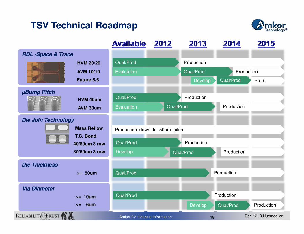
Die Join TechnologyDie Join Technology
µBump PitchµBump Pitch
HVM 40um
AVM 30um
RDL RDL --Space & TraceSpace & Trace
HVM 20/20
AVM 10/10
Future 5/5
ProductionQual/Prod
ProductionQual/ProdEvaluation
ProductionQual/Prod
ProductionQual/ProdEvaluation
Develop Qual/Prod Prod.
TSV Technical RoadmapTSV Technical Roadmap
Amkor Confidential Information Dec-12, R.Huemoeller19
Die Join TechnologyDie Join Technology
Mass Reflow
T.C. Bond
40/80um 3 row
30/60um 3 row
Die Die ThicknessThickness
>= 50um
Production down to 50um pitch
ProductionQual/Prod
ProductionQual/Prod
ProductionQual/ProdDevelop
Via DiameterVia Diameter
>= 10um
>= 6um
ProductionQual/Prod
ProductionQual/ProdDevelop
• Wafer Front Side & Back Side Integration
– Full 300mmTSV Line Installed
– Front side bump and µbump in HVM today down to 40µm pitch
– Back side integration equipment in place includes (MEOL) :
• Wafer Support System ; bond / de-bond
• Wafer Back Grind System with CMP
• Silicon Etch tool
• Both Organic and Inorganic Passivation
Summary of TSV Platform DevelopmentSummary of TSV Platform Development
Amkor Confidential Information Dec-12, R.Huemoeller20
• Both Organic and Inorganic Passivation
• CMP
• Wafer Finishes
� Au Sputtering tool
� Nickel-Gold pad finish
• Amkor Has Experience
– Wafers primarily shipped to Amkor at full thickness, 1 source as thinned/ finished
– Experience with All Major Foundries’ TSV bearing wafers
– Processed >1000 TSV bearing wafers to date through full back side wafer process
Amkor’s Core Technology & Adv. Integration Amkor’s Core Technology & Adv. Integration SchemesSchemes
Thermal &Thermal &
Cu PillarCu Pillar
TSVTSV
Amkor Confidential Information Dec-12, R.Huemoeller21
WLFOWLFOWLFOWLFO
Thermal &Thermal &Adv. MaterialsAdv. Materials
HighHigh--End FCEnd FC
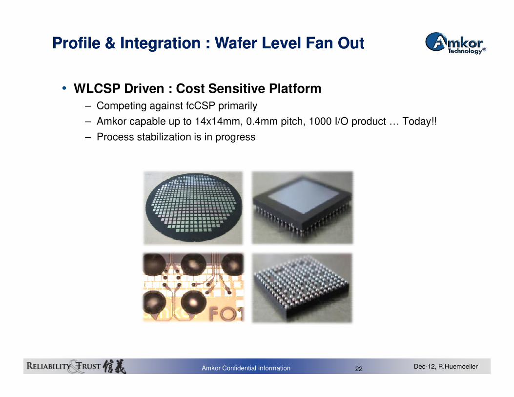
• WLCSP Driven : Cost Sensitive Platform
– Competing against fcCSP primarily
– Amkor capable up to 14x14mm, 0.4mm pitch, 1000 I/O product … Today!!
– Process stabilization is in progress
Profile & Integration : Wafer Level Fan OutProfile & Integration : Wafer Level Fan Out
Amkor Confidential Information Dec-12, R.Huemoeller22
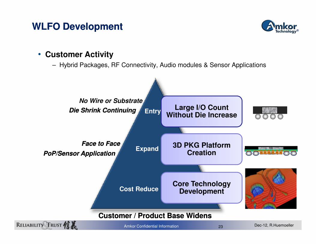
• Customer Activity
– Hybrid Packages, RF Connectivity, Audio modules & Sensor Applications
WLFO DevelopmentWLFO Development
Large I/O Count Without Die Increase
EntryDie Shrink ContinuingDie Shrink Continuing
No Wire or Substrate
Amkor Confidential Information Dec-12, R.Huemoeller23
3D PKG Platform Creation
Core Technology Development
Expand
Cost Reduce
Die
Die
Face to FaceFace to Face
Customer / Product Base WidensCustomer / Product Base Widens
PoP/Sensor Application PoP/Sensor Application
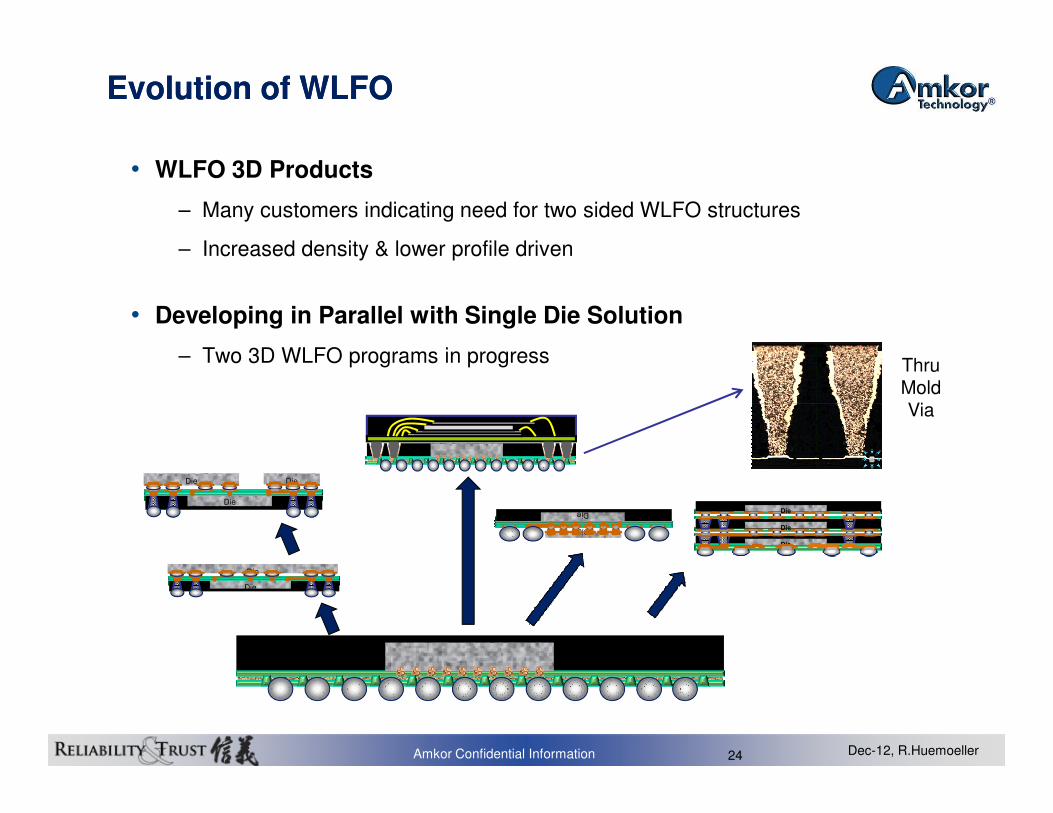
• WLFO 3D Products
– Many customers indicating need for two sided WLFO structures
– Increased density & lower profile driven
• Developing in Parallel with Single Die Solution
– Two 3D WLFO programs in progress Thru Mold Via
Evolution of WLFOEvolution of WLFO
Amkor Confidential Information Dec-12, R.Huemoeller24
Die
Die
.
3D-WLFO Benefits
H
Die
Die
Die
Die
Die
Die
3D-WLFO Benefits
Die
Die
Via
FaceFace--toto--FaceFace
3D Sensor3D Sensor
Standard WLFOStandard WLFO
K
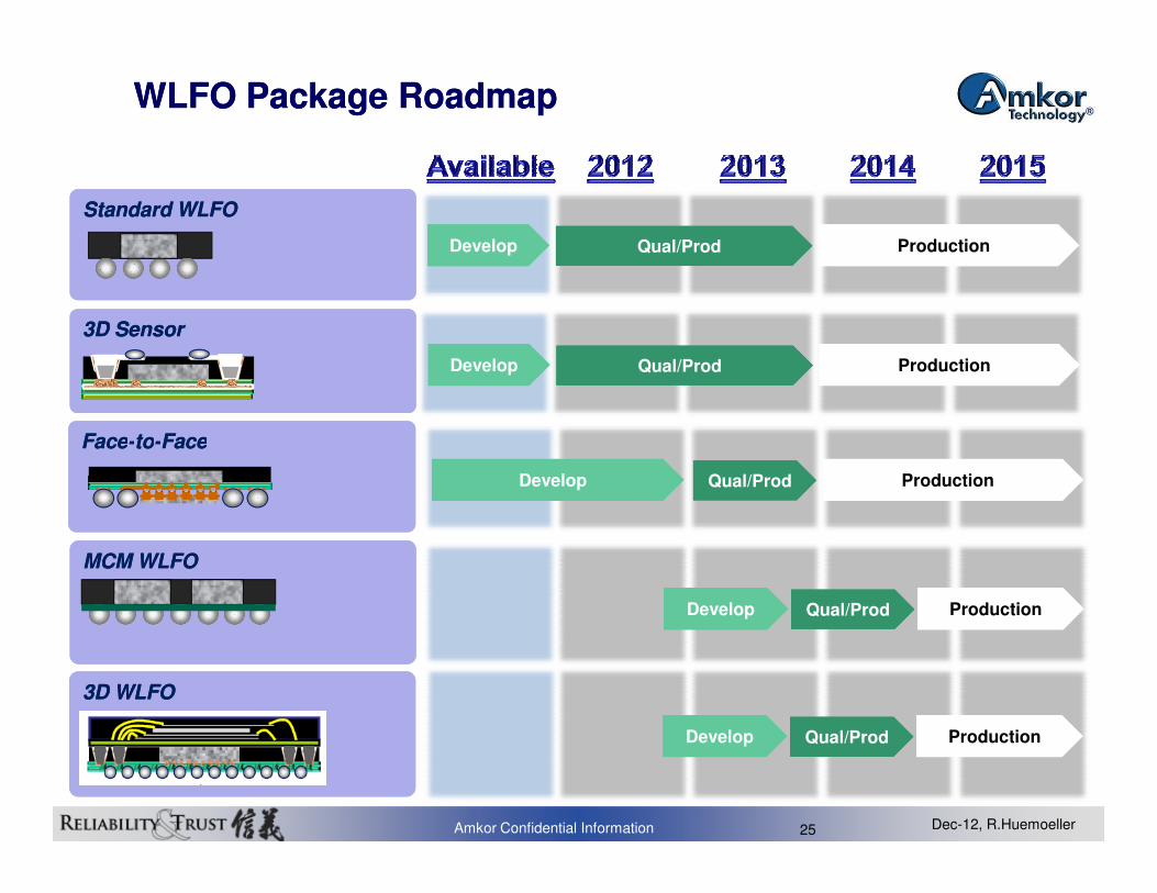
WLFO Package RoadmapWLFO Package Roadmap
ProductionQual/ProdDevelop
ProductionQual/ProdDevelop
Amkor Confidential Information Dec-12, R.Huemoeller25
FaceFace--toto--FaceFace
MCM WLFOMCM WLFO
3D WLFO3D WLFO
ProductionQual/ProdDevelop
ProductionQual/ProdDevelop
ProductionQual/ProdDevelop
Amkor’s Core Technology & Adv. Integration Amkor’s Core Technology & Adv. Integration SchemesSchemes
Thermal &Thermal &
Cu PillarCu Pillar
TSVTSV
Amkor Confidential Information Dec-12, R.Huemoeller26
WLFOWLFO
Thermal &Thermal &Adv. MaterialsAdv. Materials
HighHigh--End FCEnd FCHighHigh--End FCEnd FC
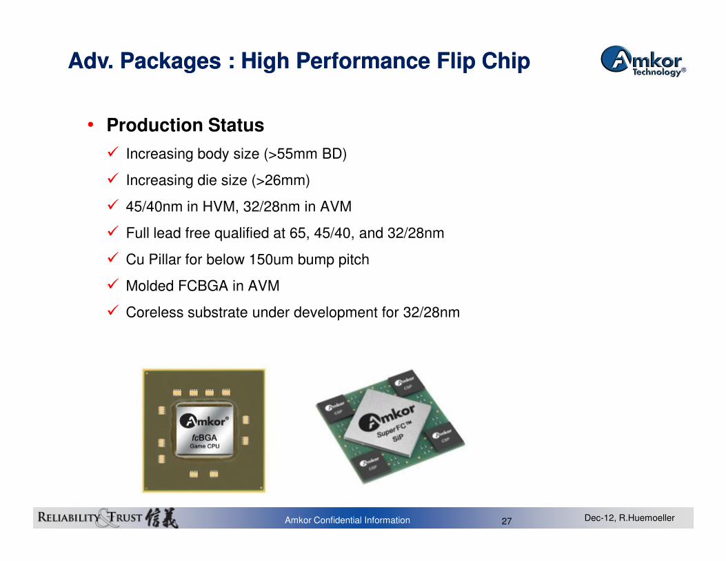
• Production Status
� Increasing body size (>55mm BD)
� Increasing die size (>26mm)
� 45/40nm in HVM, 32/28nm in AVM
� Full lead free qualified at 65, 45/40, and 32/28nm
� Cu Pillar for below 150um bump pitch
� Molded FCBGA in AVM
Adv. Packages : High Performance Flip ChipAdv. Packages : High Performance Flip Chip
Amkor Confidential Information Dec-12, R.Huemoeller27
� Molded FCBGA in AVM
� Coreless substrate under development for 32/28nm
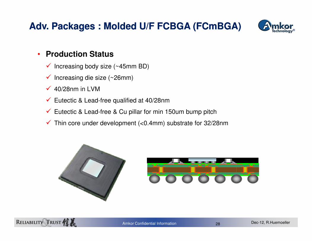
• Production Status
� Increasing body size (~45mm BD)
� Increasing die size (~26mm)
� 40/28nm in LVM
� Eutectic & Lead-free qualified at 40/28nm
� Eutectic & Lead-free & Cu pillar for min 150um bump pitch
� Thin core under development (<0.4mm) substrate for 32/28nm
Adv. Packages : Molded U/F FCBGA (Adv. Packages : Molded U/F FCBGA (FCmBGAFCmBGA))
Amkor Confidential Information Dec-12, R.Huemoeller28
� Thin core under development (<0.4mm) substrate for 32/28nm
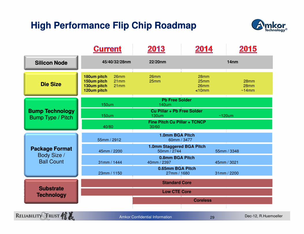
High Performance Flip Chip RoadmapHigh Performance Flip Chip Roadmap
Bump TechnologyBump TechnologyBump Type / PitchBump Type / Pitch
180um pitch 26mm 26mm 28mm150um pitch 21mm 25mm 25mm 28mm130um pitch 21mm 26mm 28mm120um pitch <10mm ~14mm
45/40/32/28nm 22/20nm 14nm
Cu Pillar + Pb Free Solder150um 130um ~120um
Pb Free Solder 150um 140um
Die SizeDie Size
Silicon NodeSilicon Node
Amkor Confidential Information Dec-12, R.Huemoeller29
Bump Type / PitchBump Type / Pitch
Package FormatPackage FormatBody Size / Ball Count
1.0mm BGA Pitch55mm / 2912 60mm / 3477
0.8mm BGA Pitch31mm / 1444 40mm / 2397 45mm / 3021
0.65mm BGA Pitch23mm / 1150 27mm / 1680 31mm / 2200
1.0mm Staggered BGA Pitch45mm / 2200 50mm / 2744 55mm / 3348
150um 130um ~120um
Fine Pitch Cu Pillar + TCNCP40/80 30/60
Substrate Substrate TechnologyTechnology
Low CTE Core
Standard Core
Coreless
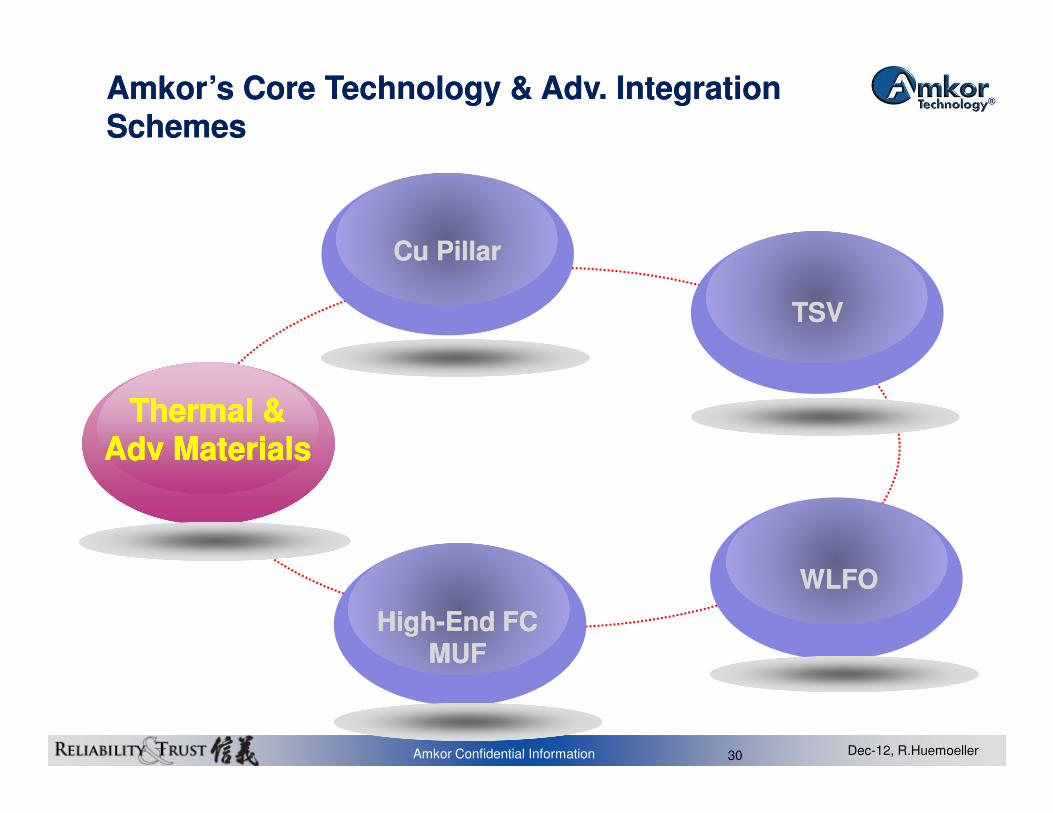
Amkor’s Core Technology & Adv. Integration Amkor’s Core Technology & Adv. Integration SchemesSchemes
Cu PillarCu Pillar
TSVTSV
Thermal &Thermal &Thermal &Thermal &
Amkor Confidential Information Dec-12, R.Huemoeller30
WLFOWLFO
HighHigh--End FCEnd FCMUFMUF
Thermal &Thermal &Adv MaterialsAdv Materials
Thermal &Thermal &Adv MaterialsAdv Materials
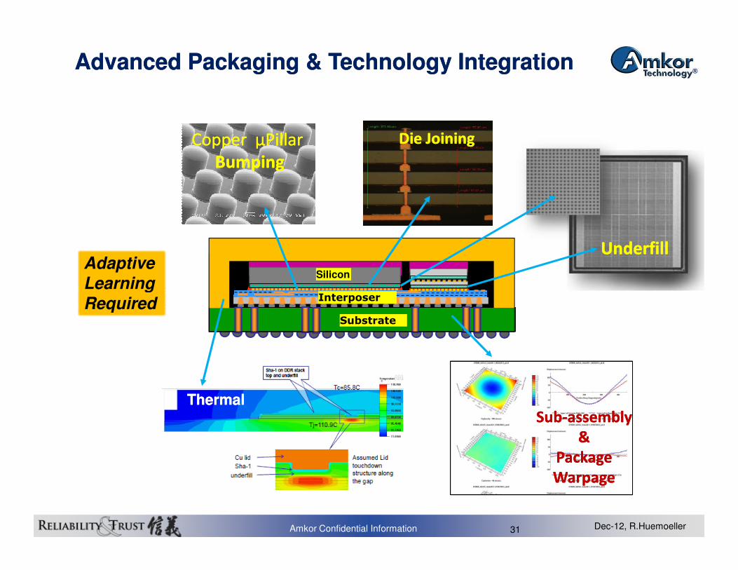
Copper µPillar Copper µPillar
BumpingBumping
Underfill Underfill
Silicon
Die JoiningDie Joining
Adaptive Learning Adaptive Learning
Advanced Packaging & Technology IntegrationAdvanced Packaging & Technology Integration
Amkor Confidential Information Dec-12, R.Huemoeller31
SubSub--assembly assembly
& &
Package Package
WarpageWarpage
ThermalThermal
Substrate
InterposerLearning RequiredLearning Required
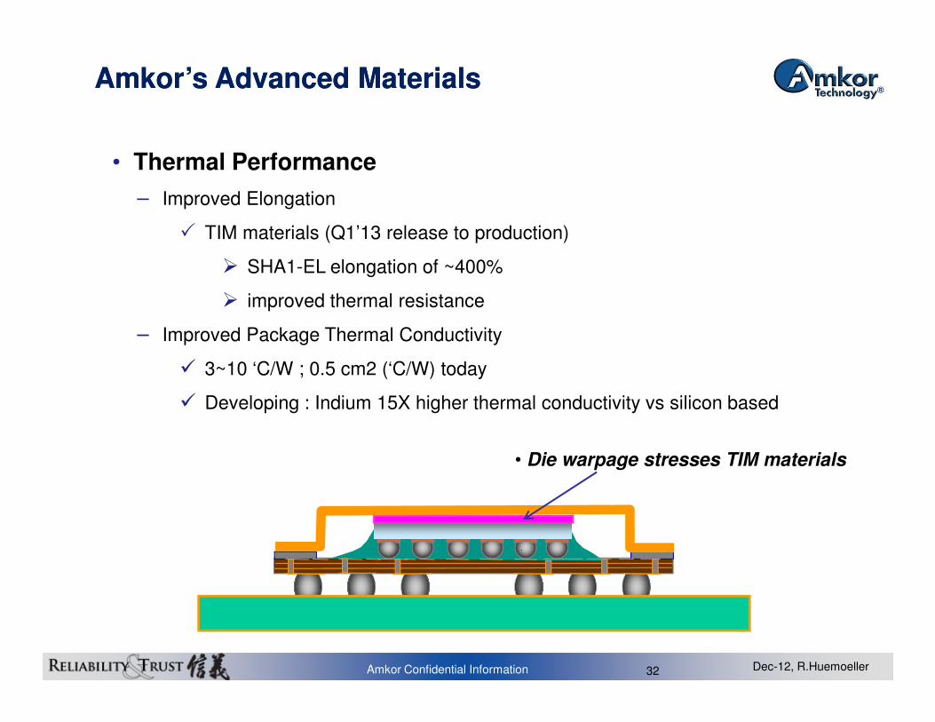
• Thermal Performance
– Improved Elongation
� TIM materials (Q1’13 release to production)
� SHA1-EL elongation of ~400%
� improved thermal resistance
– Improved Package Thermal Conductivity
� 3~10 ‘C/W ; 0.5 cm2 (‘C/W) today
Amkor’s Advanced MaterialsAmkor’s Advanced Materials
Amkor Confidential Information Dec-12, R.Huemoeller32
• Die warpage stresses TIM materials
.
� 3~10 ‘C/W ; 0.5 cm2 (‘C/W) today
� Developing : Indium 15X higher thermal conductivity vs silicon based
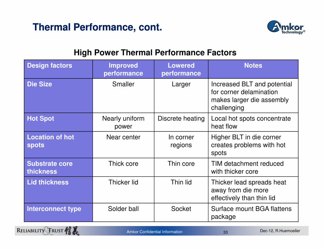
High Power Thermal Performance Factors
Design factors Improved
performance
Lowered
performance
Notes
Die Size Smaller Larger Increased BLT and potential
for corner delamination
makes larger die assembly
challenging
Hot Spot Nearly uniform
power
Discrete heating Local hot spots concentrate
heat flow
Thermal Performance, cont.Thermal Performance, cont.
Amkor Confidential Information Dec-12, R.Huemoeller33
power heat flow
Location of hot
spots
Near center In corner
regions
Higher BLT in die corner
creates problems with hot
spots
Substrate core
thickness
Thick core Thin core TIM detachment reduced
with thicker core
Lid thickness Thicker lid Thin lid Thicker lead spreads heat
away from die more
effectively than thin lid
Interconnect type Solder ball Socket Surface mount BGA flattens
package
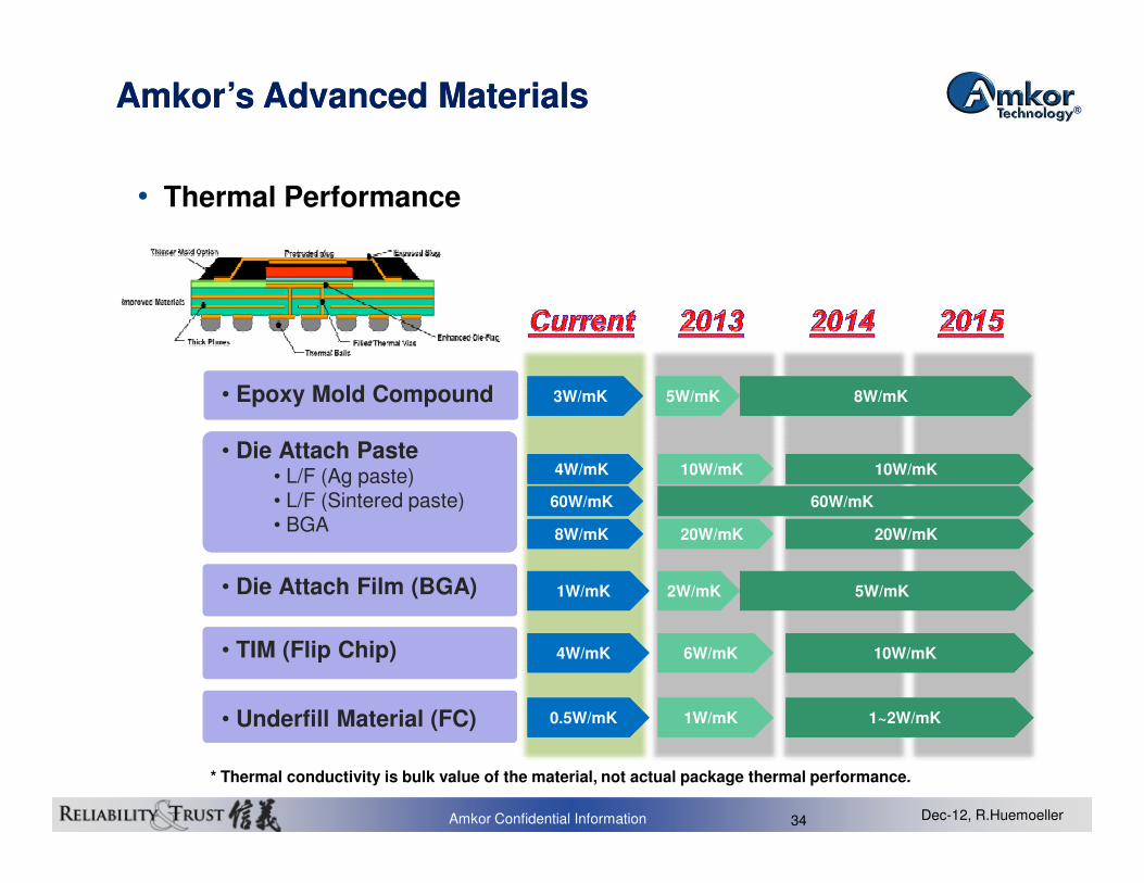
8W/mK3W/mK 5W/mK• Epoxy Mold Compound
• Die Attach Paste
Amkor’s Advanced MaterialsAmkor’s Advanced Materials
• Thermal Performance
Amkor Confidential Information Dec-12, R.Huemoeller34
• Die Attach Paste • L/F (Ag paste)• L/F (Sintered paste)• BGA
• Die Attach Film (BGA)
• TIM (Flip Chip)
• Underfill Material (FC) 1~2W/mK0.5W/mK 1W/mK
10W/mK4W/mK 6W/mK
5W/mK1W/mK 2W/mK
10W/mK4W/mK 10W/mK
60W/mK60W/mK
20W/mK8W/mK 20W/mK
* Thermal conductivity is bulk value of the material, not actual package thermal performance.
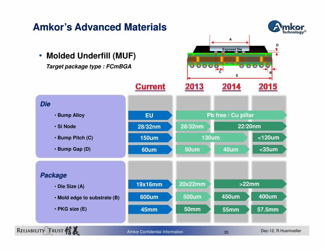
Amkor’s Advanced MaterialsAmkor’s Advanced Materials
Pb free / Cu pillar
22/20nm28/32nm
DieDie
• Bump Alloy
• Si Node
C
Exposed Die
A
D
BE
Target package type : FCmBGA
EU
28/32nm
• Molded Underfill (MUF)
Amkor Confidential Information Dec-12, R.Huemoeller35
22/20nm28/32nm
<120um130um
<35um50um
450um500um
57.5mm50mm
>22mm20x22mm
• Si Node
• Bump Pitch (C)
• Bump Gap (D)
PackagePackage
• Die Size (A)
• Mold edge to substrate (B)
• PKG size (E) 50mm
28/32nm
150um
60um
19x16mm
600um
45mm
40um
400um
55mm
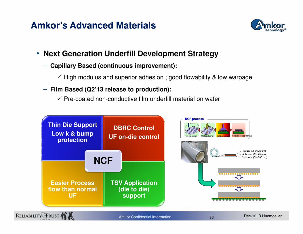
NCF process
Amkor’s Advanced MaterialsAmkor’s Advanced Materials
• Next Generation Underfill Development Strategy
– Capillary Based (continuous improvement):
� High modulus and superior adhesion ; good flowability & low warpage
– Film Based (Q2’13 release to production):
� Pre-coated non-conductive film underfill material on wafer
Amkor Confidential Information Dec-12, R.Huemoeller36
Thin Die Support
Low k & bump protection
DBRC Control
UF on-die control
Easier Process flow than normal
UF
TSV Application (die to die)
support
NCF
NCF process
Wafer dicing TC bonding Post cure (optional)Pre-applied

Thank You!Enabling a
Microelectronic
World®
Thank You!