Embed Size (px)
Citation preview
EMD56164PC-xxx 256Mb MOBILE DDR SDRAM
Preliminary :Nov, 22, 2012 - 1 -
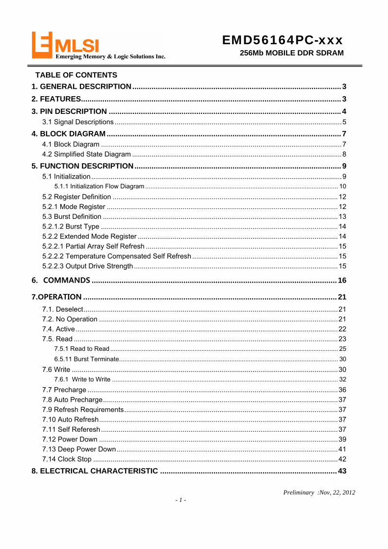
TABLE OF CONTENTS
1. GENERAL DESCRIPTION .................................................................................................. 3
2. FEATURES .......................................................................................................................... 3
3. PIN DESCRIPTION ............................................................................................................. 4
3.1 Signal Descriptions ..................................................................................................................... 5
4. BLOCK DIAGRAM .............................................................................................................. 7
4.1 Block Diagram ............................................................................................................................ 7
4.2 Simplified State Diagram ............................................................................................................ 8
5. FUNCTION DESCRIPTION ................................................................................................. 9
5.1 Initialization ................................................................................................................................. 9
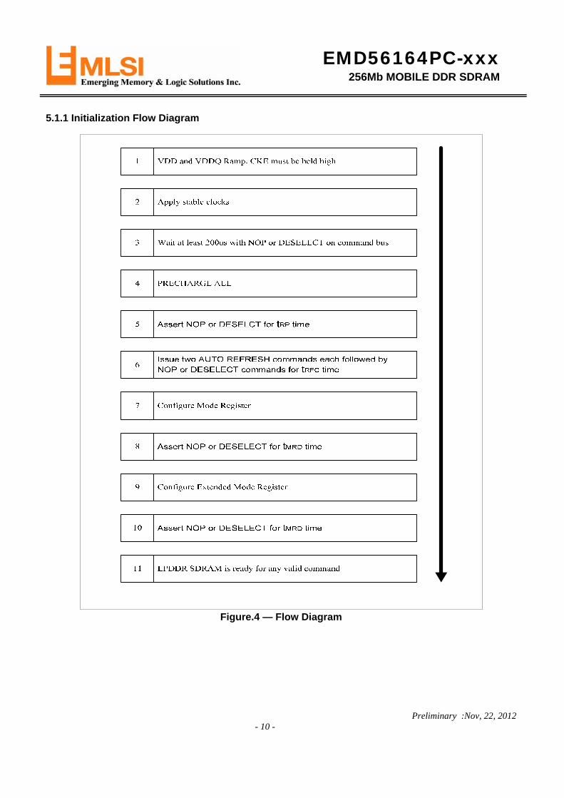
5.1.1 Initialization Flow Diagram .............................................................................................................. 10
5.2 Register Definition .................................................................................................................... 12
5.2.1 Mode Register ....................................................................................................................... 12
5.3 Burst Definition ......................................................................................................................... 13
5.2.1.2 Burst Type .......................................................................................................................... 14
5.2.2 Extended Mode Register ....................................................................................................... 14
5.2.2.1 Partial Array Self Refresh ................................................................................................... 15
5.2.2.2 Temperature Compensated Self Refresh ........................................................................... 15
5.2.2.3 Output Drive Strength ......................................................................................................... 15
6. COMMANDS ................................................................................................................... 16
7.OPERATION ....................................................................................................................... 21
7.1. Deselect ................................................................................................................................... 21
7.2. No Operation ........................................................................................................................... 21
7.4. Active ....................................................................................................................................... 22
7.5. Read ........................................................................................................................................ 23
7.5.1 Read to Read .................................................................................................................................. 25
6.5.11 Burst Terminate ............................................................................................................................. 30
7.6 Write ......................................................................................................................................... 30
7.6.1 Write to Write ................................................................................................................................. 32
7.7 Precharge ................................................................................................................................. 36
7.8 Auto Precharge ......................................................................................................................... 37
7.9 Refresh Requirements .............................................................................................................. 37
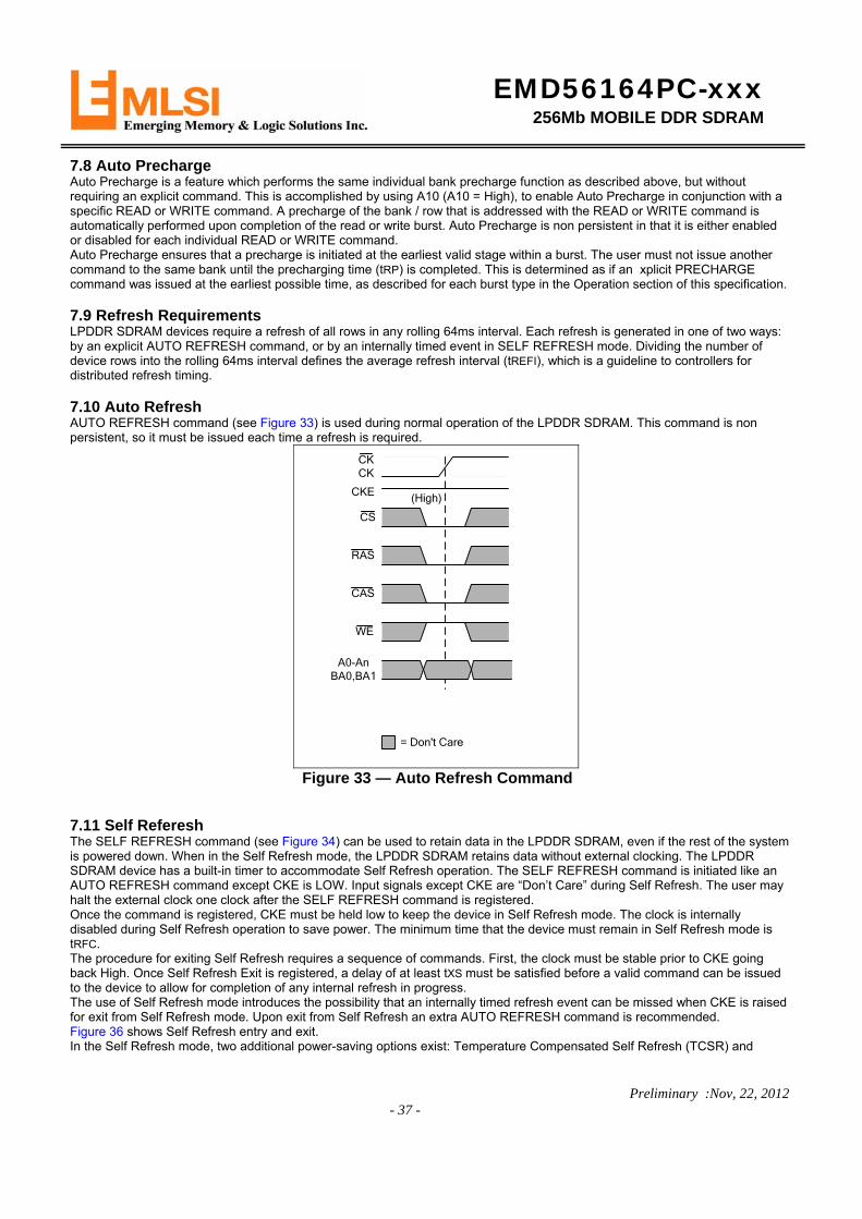
7.10 Auto Refresh ........................................................................................................................... 37
7.11 Self Referesh .......................................................................................................................... 37
7.12 Power Down ........................................................................................................................... 39
7.13 Deep Power Down .................................................................................................................. 41
7.14 Clock Stop .............................................................................................................................. 42
8. ELECTRICAL CHARACTERISTIC ................................................................................... 43
EMD56164PC-xxx 256Mb MOBILE DDR SDRAM
Preliminary :Nov, 22, 2012 - 2 -
8.1 Absolute Maximum Ratings ...................................................................................................... 43
8.2 Input/Output Capacitance ......................................................................................................... 43
8.3 Electrical Characteristics and AC/DC Operating Conditions .................................................... 44
8.3.1 Electrical Characteristics and AC/DC Operating Conditions .......................................................... 44
8.4 IDD Specification Parameters and Test Conditions .................................................................. 45
8.4.1 IDD Specification Parameters and Test Conditions ....................................................................... 45
8.5 AC Timings ............................................................................................................................... 47
8.5.2 Output Slew Rate Characteristics ................................................................................................... 51
7.5.3 AC Overshoot/Undershoot Specification ........................................................................................ 51
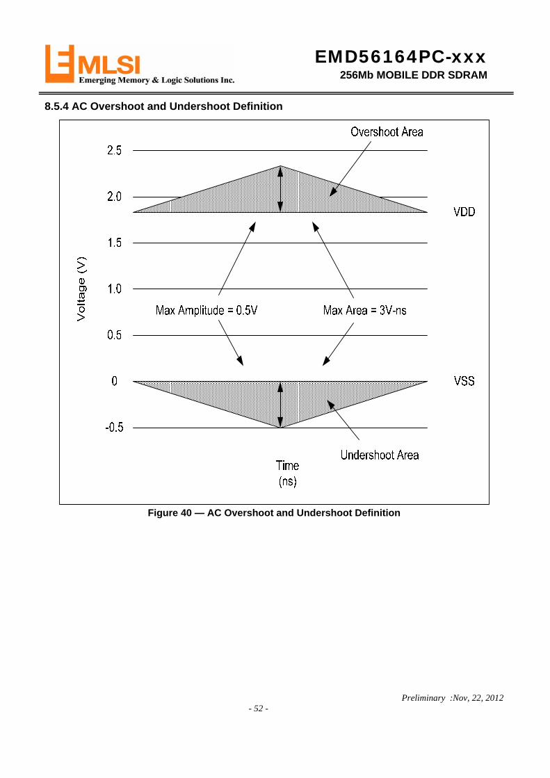
8.5.4 AC Overshoot and Undershoot Definition ....................................................................................... 52
9.PACKAGE DIMENSION ..................................................................................................... 53
10. ORDERING INFORMATION ........................................................................................... 54
11. REVISION HISTORY ............................................................................................... 55
EMD56164PC-xxx 256Mb MOBILE DDR SDRAM
Preliminary :Nov, 22, 2012 - 3 -
1. GENERAL DESCRIPTION This EMD56164PC is 268,435,456 bits synchronous double data rate Dynamic RAM. Each 67,108,864 bits bank is organized as 8,192 rows by 512 columns by 16 bits, fabricated with EMLSI’s high performance CMOS technology. This device uses a double data rate architecture to achieve high- speed operation. The double data rate architecture is essentially a 2n-prefetch architecture with an interface designed to transfer two data words per clock cycle at the I/O balls. Range of operating frequencies, programmable burst lengths and programmable latencies allow the same device to be useful for a variety of high bandwidth and high performance memory system applications.
2. FEATURES
EMD56164PC VDD/VDDQ = 1.7~1.95V Data width: x16 Clock rate: 200MHz,166MHz , 133MHz Partial Array Self-Refresh(PASR) Auto Temperature Compensated Self-Refresh(ATCSR) Power Down Mode Deep Power Down Mode (DPD Mode) Programmable output buffer driver strength Four internal banks for concurrent operation Data mask (DM) for write data Clock Stop capability during idle periods Auto Pre-charge option for each burst access Double data rate for data output
Differential clock inputs (CK and CK )
Bidirectional, data strobe (DQS)
CAS Latency: 2 and 3
Burst Length: 2, 4, 8 and 16 Burst Type: Sequential or Interleave 64 ms Refresh period Interface: LVCMOS Operating Temperature Range Extended (-25 to + 85 )℃ ℃
Industrial (-40 to + 85 )℃ ℃ Auto Address Generation Mode
EMD56164PC-xxx 256Mb MOBILE DDR SDRAM
Preliminary :Nov, 22, 2012 - 4 -
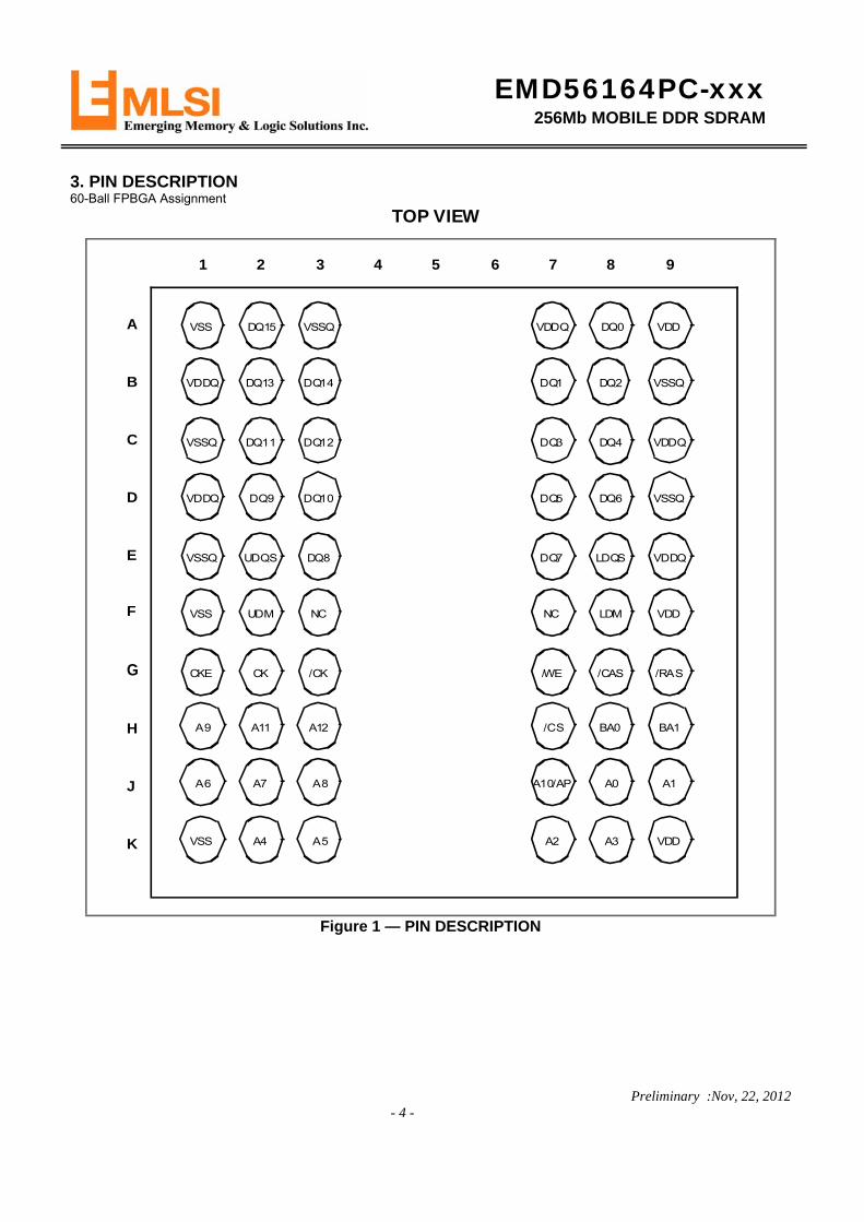
3. PIN DESCRIPTION 60-Ball FPBGA Assignment
VSS DQ15 VSSQ
VDDQ DQ13 DQ14
VSSQ DQ11 DQ12
VDDQ DQ9 DQ10
VSSQ UDQS DQ8
VSS UDM NC
CKE CK /CK
A9 A11 A12
1 2 3 4 5 6
A
B
C
D
E
F
G
H
A6 A7 A8J
TOP VIEW
K
7 8 9
VSS A4 A5
VDDQ DQ0 VDD
DQ1 DQ2 VSSQ
DQ3 DQ4 VDDQ
DQ5 DQ6 VSSQ
DQ7 LDQS VDDQ
NC LDM VDD
/WE /CAS /RAS
/CS BA0 BA1
A10/AP A0 A1
A2 A3 VDD
Figure 1 — PIN DESCRIPTION
EMD56164PC-xxx 256Mb MOBILE DDR SDRAM
Preliminary :Nov, 22, 2012 - 5 -
3.1 Signal Descriptions
SIGNAL NAME TYPE DESCRIPTION
CK,/CK Input
Clock: CK and CK are differential clock inputs. All address and control input signals are sampled on the crossing of the positive edge of CK and negative edge of CK. Input and output data is referenced to the crossing of CK and CK (both directions of crossing). Internal clock signals are derived from CK/CK.
CKE Input
Clock Enable: CKE HIGH activates, and CKE LOW deactivates internal clock signals, and device input buffers and output drivers. Taking CKE LOW provides PRECHARGE POWER-DOWN and SELF REFRESH operation (all banks idle), or ACTIVE POWERDOWN (row ACTIVE in any bank). CKE is synchronous for all functions except for SELF REFRESH EXIT, which is achieved asynchronously. Input buffers, excluding CK, CK and CKE, are disabled during power-down and self refresh mode which are contrived for low standby power consumption.
/CS Input
Chip Select: CS enables (registered LOW) and disables (registered HIGH) the command decoder. All commands are masked when CS is registered HIGH. CS provides for external bank selection on systems with multiple banks. CS is considered part of the command code.
/RAS,/CAS,/WE Input Command Inputs: RAS, CAS and WE (along with CS) define the command being entered.
LDM,UDM Input
Input Data Mask: DM is an input mask signal for write data. Input data is masked when DM is sampled HIGH along with that input data during a WRITE access. DM is sampled on both edges of DQS. Although DM pins are input-only, the DM loading matches the DQ and DQS loading. For x16 devices, LDM corresponds to the data on DQ0-DQ7, UDM corresponds to the data on DQ8-DQ15.
BA0,BA1 Input Bank Address Inputs: BA0 and BA1 define to which bank an ACTIVE, READ, WRITE or PRECHARGE command is being applied.
A [n : 0]
Input Address Inputs: provide the row address for ACTIVE commands, and the column address and AUTO PRECHARGE bit for READ / WRITE commands, to select one location out of the memory array in the respective bank. The address inputs also provide the opcode during a MODE REGISTER SET command.
DQ0-DQ15 I/O Data Bus: Input / Output
LDQS,UDQS I/O
Data Strobe: Output with read data, input with write data. Edge-aligned with read data, centered with write data. Used to capture write data. LDQS corresponds to the data on DQ0-DQ7, UDQS corresponds to the data on DQ8-DQ15.
NC - No Connect: No internal electrical connection is presen
VDDQ Supply I/O Power Supply
VSSQ Supply I/O Ground
VDD Supply Power Supply
VSS Supply Ground
Table 1 — Signal Descriptions
EMD56164PC-xxx 256Mb MOBILE DDR SDRAM
Preliminary :Nov, 22, 2012 - 6 -
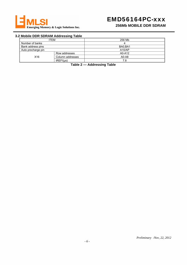
3.2 Mobile DDR SDRAM Addressing Table ITEM 256 Mb
Number of banks 4 Bank address pins BA0,BA1 Auto precharge pin A10/AP
X16 Row addresses A0-A12 Column addresses A0-A8 tREFI(µs) 7.8
Table 2 — Addressing Table
EMD56164PC-xxx 256Mb MOBILE DDR SDRAM
Preliminary :Nov, 22, 2012 - 7 -
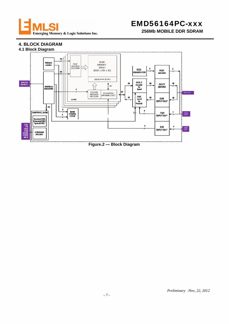
4. BLOCK DIAGRAM 4.1 Block Diagram
Figure.2 — Block Diagram
EMD56164PC-xxx 256Mb MOBILE DDR SDRAM
Preliminary :Nov, 22, 2012 - 8 -
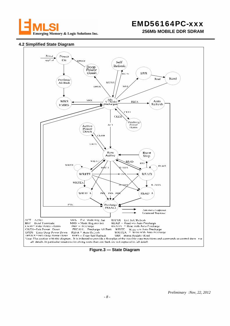
4.2 Simplified State Diagram
Figure.3 — State Diagram
EMD56164PC-xxx 256Mb MOBILE DDR SDRAM
Preliminary :Nov, 22, 2012 - 9 -
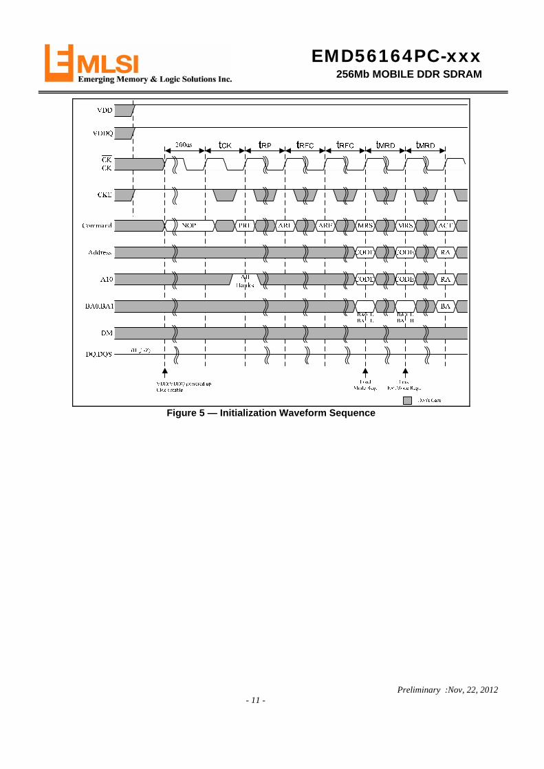
5. FUNCTION DESCRIPTION The LPDDR SDRAM is a high speed CMOS, dynamic random-access memory internally configured as a quad-bank DRAM. These devices contain the following number of bits: 256 Mb has 268,435,456 bits The LPDDR SDRAM uses a double data rate architecture to achieve high speed operation. The double data rate architecture is essentially a 2n prefetch architecture with an interface designed to transfer two data words per clock cycle at the I/O pins. A single read or write access for the LPDDR SDRAM effectively consists of a single 2n-bit wide, one clock cycle data transfer at the internal DRAM core and two corresponding n-bit wide, one-half-clockcycle data transfers at the I/O pins. Read and write accesses to the LPDDR SDRAM are burst oriented; accesses start at a selected location and continue for a programmed number of locations in a programmed sequence. Accesses begin with the registration of an ACTIVE command, which is then followed by a READ or WRITE command. The address bits registered coincident with the ACTIVE command are used to select the bank and the row to be accessed. The address bits registered coincident with the READ or WRITE command are used to select the bank and the starting column location for the burst access. Prior to normal operation, the LPDDR SDRAM must be initialized. The following section provides detailed information covering device initialization, register definition, command description and device operation. 5.1 Initialization LPDDR SDRAMs must be powered up and initialized in a predefined manner. Operations procedures other than those specified may result in undefined operation. If there is any interruption to the device power, the initialization routine should be followed. The steps to be followed for device initialization are listed below. The Initialization Flow diagram is shown in Figure 4, and the Initialization Flow sequence in Figure 5. The Mode Register and Extended Mode Register do not have default values. If they are not programmed during the initialization sequence, it may lead to unspecified operation. The clock stop feature is not available until the device has been properly initialized from Steps 1 through 11. 1. Provide power, the device core power (VDD) and the device I/O power (VDDQ) must be brought up simultaneously to prevent device latch-up. Although not required, it is recommended that VDD and VDDQ are from the same power source. Also assert and hold Clock Enable (CKE) to a LV-CMOS logic high level 2. Once the system has established consistent device power and CKE is driven high, it is safe to apply stable clock 3. There must be at least 200 μs of valid clocks before any command may be given to the DRAM. During this time NOP or DESELECT commands must be issued on the command bus. 4. Issue a PRECHARGE ALL command. 5. Provide NOPs or DESELECT commands for at least tRP time. 6. Issue an AUTO REFRESH command followed by NOPs or DESELECT command for at least tRFC time. Issue the second AUTO REFRESH command followed by NOPs or DESELECT command for at least tRFC time. Note as part of the initialization sequence there must be two auto refresh commands issued. The typical flow is to issue them at Step 6, but they may also be issued between steps 10 and 11. 7. Using the MRS command, load the base mode register. Set the desired operating modes. 8. Provide NOPs or DESELECT commands for at least tMRD time. 9. Using the MRS command, program the extended mode register for the desired operating modes. Note the order of the base and extended mode register programming is not important. 10. Provide NOP or DESELCT commands for at least tMRD time. 11. The DRAM has been properly initialized and is ready for any valid command.
EMD56164PC-xxx 256Mb MOBILE DDR SDRAM
Preliminary :Nov, 22, 2012 - 10 -
5.1.1 Initialization Flow Diagram
Figure.4 — Flow Diagram
EMD56164PC-xxx 256Mb MOBILE DDR SDRAM
Preliminary :Nov, 22, 2012 - 11 -
Figure 5 — Initialization Waveform Sequence
EMD56164PC-xxx 256Mb MOBILE DDR SDRAM
Preliminary :Nov, 22, 2012 - 12 -
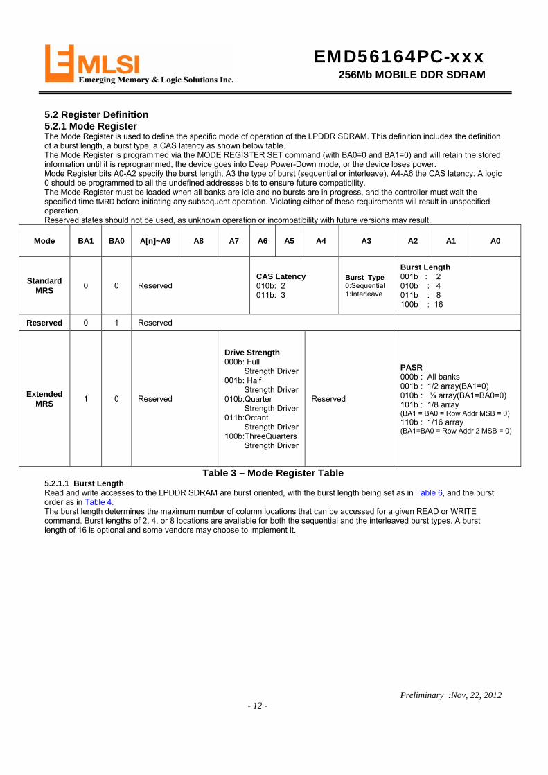
5.2 Register Definition 5.2.1 Mode Register The Mode Register is used to define the specific mode of operation of the LPDDR SDRAM. This definition includes the definition of a burst length, a burst type, a CAS latency as shown below table. The Mode Register is programmed via the MODE REGISTER SET command (with BA0=0 and BA1=0) and will retain the stored information until it is reprogrammed, the device goes into Deep Power-Down mode, or the device loses power. Mode Register bits A0-A2 specify the burst length, A3 the type of burst (sequential or interleave), A4-A6 the CAS latency. A logic 0 should be programmed to all the undefined addresses bits to ensure future compatibility. The Mode Register must be loaded when all banks are idle and no bursts are in progress, and the controller must wait the specified time tMRD before initiating any subsequent operation. Violating either of these requirements will result in unspecified operation. Reserved states should not be used, as unknown operation or incompatibility with future versions may result.
Mode BA1 BA0 A[n]~A9 A8 A7 A6 A5 A4 A3 A2 A1 A0
Standard MRS
0 0 Reserved CAS Latency 010b: 2 011b: 3
Burst Type 0:Sequential 1:Interleave
Burst Length 001b : 2 010b : 4 011b : 8 100b : 16
Reserved 0 1 Reserved
Extended MRS
1 0 Reserved
Drive Strength 000b: Full
Strength Driver001b: Half
Strength Driver010b:Quarter
Strength Driver011b:Octant
Strength Driver100b:ThreeQuarters
Strength Driver
Reserved
PASR 000b : All banks 001b : 1/2 array(BA1=0) 010b : ¼ array(BA1=BA0=0) 101b : 1/8 array (BA1 = BA0 = Row Addr MSB = 0) 110b : 1/16 array (BA1=BA0 = Row Addr 2 MSB = 0)
Table 3 – Mode Register Table 5.2.1.1 Burst Length Read and write accesses to the LPDDR SDRAM are burst oriented, with the burst length being set as in Table 6, and the burst order as in Table 4. The burst length determines the maximum number of column locations that can be accessed for a given READ or WRITE command. Burst lengths of 2, 4, or 8 locations are available for both the sequential and the interleaved burst types. A burst length of 16 is optional and some vendors may choose to implement it.
EMD56164PC-xxx 256Mb MOBILE DDR SDRAM
Preliminary :Nov, 22, 2012 - 13 -
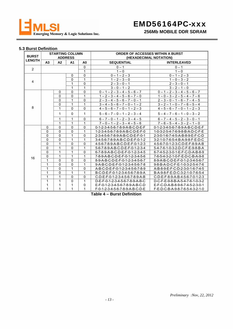
5.3 Burst Definition
BURST LENGTH
STARTING COLUMN ADDRESS
ORDER OF ACCESSES WITHIN A BURST (HEXADECIMAL NOTATION)
A3 A2 A1 A0 SEQUENTIAL INTERLEAVED
2 0 0 – 1 0 – 1 1 1 – 0 1 – 0
4
0 0 0 – 1 – 2 – 3 0 – 1 – 2 – 3 0 1 1 – 2 – 3 – 0 1 – 0 – 3 – 2 1 0 2 – 3 – 0 – 1 2 – 3 – 0 – 1 1 1 3 – 0 – 1 – 2 3 – 2 – 1 – 0
8
0 0 0 0 – 1 – 2 – 3 – 4 – 5 – 6 – 7 0 – 1 – 2 – 3 – 4 – 5 – 6 – 7 0 0 1 1 – 2 – 3 – 4 – 5 – 6 – 7 – 0 1 – 0 – 3 – 2 – 5 – 4 – 7 – 6 0 1 0 2 – 3 – 4 – 5 – 6 – 7 – 0 – 1 2 – 3 – 0 – 1 – 6 – 7 – 4 – 5 0 1 1 3 – 4 – 5 – 6 – 7 – 0 – 1 – 2 3 – 2 – 1 – 0 – 7 – 6 – 5 – 4 1 0 0 4 – 5 – 6 – 7 – 0 – 1 – 2 – 3 4 – 5 – 6 – 7 – 0 – 1 – 2 – 3
1 0 1 5 – 6 – 7 – 0 – 1 – 2 – 3 – 4 5 – 4 – 7 – 6 – 1 – 0 – 3 – 2
1 1 0 6 – 7 – 0 – 1 – 2 – 3 – 4 – 5 6 – 7 – 4 – 5 – 2 – 3 – 0 – 1 1 1 1 7 – 0 – 1 – 2 – 3 – 4 – 5 – 6 7 – 6 – 5 – 4 – 3 – 2 – 1 – 0
16
0 0 0 0 0-1-2-3-4-5-6-7-8-9-A-B-C-D-E-F 0-1-2-3-4-5-6-7-8-9-A-B-C-D-E-F 0 0 0 1 1-2-3-4-5-6-7-8-9-A-B-C-D-E-F-0 1-0-3-2-5-4-7-6-9-8-B-A-D-C-F-E 0 0 1 0 2-3-4-5-6-7-8-9-A-B-C-D-E-F-0-1 2-3-0-1-6-7-4-5-A-B-8-9-E-F-C-D 0 0 1 1 3-4-5-6-7-8-9-A-B-C-D-E-F-0-1-2 3-2-1-0-7-6-5-4-B-A-9-8-F-E-D-C 0 1 0 0 4-5-6-7-8-9-A-B-C-D-E-F-0-1-2-3 4-5-6-7-0-1-2-3-C-D-E-F-8-9-A-B 0 1 0 1 5-6-7-8-9-A-B-C-D-E-F-0-1-2-3-4 5-4-7-6-1-0-3-2-D-C-F-E-9-8-B-A 0 1 1 0 6-7-8-9-A-B-C-D-E-F-0-1-2-3-4-5 6-7-4-5-2-3-0-1-E-F-C-D-A-B-8-9 0 1 1 1 7-8-9-A-B-C-D-E-F-0-1-2-3-4-5-6 7-6-5-4-3-2-1-0-F-E-D-C-B-A-9-8 1 0 0 0 8-9-A-B-C-D-E-F-0-1-2-3-4-5-6-7 8-9-A-B-C-D-E-F-0-1-2-3-4-5-6-7 1 0 0 1 9-A-B-C-D-E-F-0-1-2-3-4-5-6-7-8 9-8-B-A-D-C-F-E-1-0-3-2-5-4-7-6 1 0 1 0 A-B-C-D-E-F-0-1-2-3-4-5-6-7-8-9 A-B-8-9-E-F-C-D-2-3-0-1-6-7-4-5 1 0 1 1 B-C-D-E-F-0-1-2-3-4-5-6-7-8-9-A B-A-9-8-F-E-D-C-3-2-1-0-7-6-5-4 1 1 0 0 C-D-E-F-0-1-2-3-4-5-6-7-8-9-A-B C-D-E-F-8-9-A-B-4-5-6-7-0-1-2-3 1 1 0 1 D-E-F-0-1-2-3-4-5-6-7-8-9-A-B-C D-C-F-E-9-8-B-A-5-4-7-6-1-0-3-2 1 1 1 0 E-F-0-1-2-3-4-5-6-7-8-9-A-B-C-D E-F-C-D-A-B-8-9-6-7-4-5-2-3-0-1 1 1 1 1 F-0-1-2-3-4-5-6-7-8-9-A-B-C-D-E F-E-D-C-B-A-9-8-7-6-5-4-3-2-1-0
Table 4 – Burst Definition
EMD56164PC-xxx 256Mb MOBILE DDR SDRAM
Preliminary :Nov, 22, 2012 - 14 -
Notes: 1. 16-word burst length is optional. 2. For a burst length of two, A1-An selects the two data element block; A0 selects the first access within the block. 3. For a burst length of four, A2-An selects the four data element block; A0-A1 selects the first access within the block. 4. For a burst length of eight, A3-An selects the eight data element block; A0-A2 selects the first access within the block. 5. For the optional burst length of sixteen, A4-An selects the sixteen data element block; A0-A3 selects the first access within the block. 6. Whenever a boundary of the block is reached within a given sequence, the following access wraps within the block When a READ or WRITE command is issued, a block of columns equal to the burst length is effectively selected. All accesses for that burst take place within the block, meaning that the burst will wrap within the block if a boundary is reached. The block is uniquely selected by A1-An when the burst length is set to two, by A2-An when the burst length is set to 4, by A3-An when the burst length is set to 8 and A4-An when the burst length is set to 16 (where An is the most significant column address bit for a given configuration). The remaining (least significant) address bit(s) is (are) used to select the starting location within the block. The programmed burst length applies to both read and write bursts.
5.2.1.2 Burst Type Accesses within a given burst may be programmed to be either sequential or interleaved; this is referred to as the burst type and is selected via bit A3. The ordering of accesses within a burst is determined by the burst length, the burst type and the starting column address, as shown in Table 4. 5.2.1.3 Read Latency The READ latency, or CAS latency, is the delay between the registration of a READ command and the availability of the first piece of output data. The latency should be set to 3 clocks. Some vendors may offer additional options of 2 clocks and/or 4 clocks. If a READ command is registered at a clock edge n and the latency is 3 clocks, the first data element will be valid at n + 2tCK + tAC. If a READ command is registered at a clock edge n and the latency is 2 clocks, the first data element will be valid at n + tCK + tAC. Lastly, if a READ command is registered at a clock edge n and the latency is 4 clocks, the first data element will be valid at n + 3tCK + tAC. 5.2.2 Extended Mode Register The Extended Mode Register controls functions beyond those controlled by the Mode Register; these additional functions include output drive strength selection, Temperature Compensated Self Refresh (TCSR) and Partial Array Self Refresh (PASR), as shown in Figure 7. The TCSR and PASR functions are optional and some vendors may choose not to implement them. Both TCSR and PASR are effective is in Self Refresh mode only. The Extended Mode Register is programmed via the MODE REGISTER SET command (with BA1=1 and BA0=0) and will retain the stored information until it is reprogrammed, the device is put in Deep Power-Down mode, or the device loses power. The Extended Mode Register must be loaded when all banks are idle and no bursts are in progress, and the controller must wait the specified time tMRD before initiating any subsequent operation. Violating either of these requirements will result in unspecified operation. Address bits A0-A2 specify PASR, A3-A4 the TCSR, A5-A6 the Drive Strength. A logic 0 should be programmed to all the undefined addresses bits to ensure future compatibility. Reserved states should not be used, as unknown operation or incompatibility with future versions may result. Address bits A0-A2 specify PASR, A3-A4 the TCSR, A5-A7 the Drive Strength. A logic 0 should be programmed to all the undefined address bits to ensure future compatibility. Reserved states should not be used, as unknown operation or incompatibility with future versions may result.

EMD56164PC-xxx 256Mb MOBILE DDR SDRAM
Preliminary :Nov, 22, 2012 - 15 -
BA1 BA0 A[n]~A8 A7 A6 A5 A4 A3 A2 A1 A0
1 0 Reserved
Drive Strength 000b: Full
Strength Driver001b: Half
Strength Driver010b:Quarter
Strength Driver011b:Octant
Strength Driver100b:ThreeQuarters
Strength Driver
Reserved
PASR 000b : All banks 001b : 1/2 array(BA1=0) 010b : ¼ array(BA1=BA0=0) 101b : 1/8 array (BA1 = BA0 = Row Addr MSB = 0) 110b : 1/16 array (BA1=BA0 = Row Addr 2 MSB = 0)
5.2.2.1 Partial Array Self Refresh Partial Array Self Refresh (PASR) is an optional feature. With PASR, the self refresh may be restricted to a variable portion of the total array. The whole array (default), 1/2 array, or 1/4 array could be selected. Some vendors may have additional options of 1/8 and 1/16 array refreshed as well. Data outside the defined area will be lost. Address bits A0 to A2 are used to set PASR.
5.2.2.2 Temperature Compensated Self Refresh This function can be used in the LPDDR SDRAM to set refresh rates based on case temperature.This allows the system to control power as a function of temperature. Address bits A3 and A4 are used to set TCSR. Some vendors may choose to have Internal Temperature Compensated Self Refresh feature, which should automatically adjust the refresh rate based on the device temperature without any register update needed. To maintain backward compatibility, devices having internal TCSR, ignore (don’t care) the inputs to address bits A3 and A4 during EMRS programming. 5.2.2.3 Output Drive Strength The drive strength could be set to full or half or three-quarters strength via address bits A5 and A6 and A7. The I-V curves for the full drive strength and half drive strength and three-quarters drive strength are included in this document (cf. Table 17 and Table 18, Figure 45 and Figure 46 and Figure 47).
EMD56164PC-xxx 256Mb MOBILE DDR SDRAM
Preliminary :Nov, 22, 2012 - 16 -
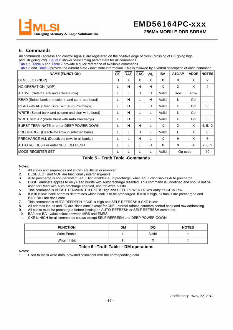
6. Commands All commands (address and control signals) are registered on the positive edge of clock (crossing of CK going high and CK going low). Figure 6 shows basic timing parameters for all commands. Table 5, Table 6 and Table 7 provide a quick reference of available commands. Table 8 and Table 9 provide the current state / next state information. This is followed by a verbal description of each command.
NAME (FUNCTION) CS RAS CAS WE BA A10/AP ADDR NOTES
DESELECT (NOP) H X X X X X X 2
NO OPERATION (NOP) L H H H X X X 2
ACTIVE (Select Bank and activate row) L L H H Valid Row Row
READ (Select bank and column and start read burst) L H L H Valid L Col
READ with AP (Read Burst with Auto Precharge) L H L H Valid H Col 3
WRITE (Select bank and column and start write burst) L H L L Valid L Col
WRITE with AP (Write Burst with Auto Precharge) L H L L Valid H Col 3
BURST TERMINATE or enter DEEP POWER DOWN L H H L X X X 4, 5,12
PRECHARGE (Deactivate Row in selected bank) L L H L Valid L X 6
PRECHARGE ALL (Deactivate rows in all banks) L L H L X H X 6
AUTO REFRESH or enter SELF REFRESH L L L H X X X 7, 8, 9
MODE REGISTER SET L L L L Valid Op-code 10
Table 5 – Truth Table -Commands Notes: 1. All states and sequences not shown are illegal or reserved. 2. DESELECT and NOP are functionally interchangeable. 3. Auto precharge is non-persistent. A10 High enables Auto precharge, while A10 Low disables Auto precharge. 4. Burst Terminate applies to only Read bursts with Autoprecharge disabled. This command is undefined and should not be
used for Read with Auto precharge enabled, and for Write bursts. 5. This command is BURST TERMINATE if CKE is High and DEEP POWER DOWN entry if CKE is Low. 6. If A10 is low, bank address determines which bank is to be precharged. If A10 is high, all banks are precharged and
BA0~BA1 are don’t care. 7. This command is AUTO REFRESH if CKE is High and SELF REFRESH if CKE is low. 8. All address inputs and I/O are ‘don’t care’ except for CKE. Internal refresh counters control bank and row addressing. 9. All banks must be precharged before issuing an AUTO-REFRESH or SELF REFRESH command. 10. BA0 and BA1 value select between MRS and EMRS. 11. CKE is HIGH for all commands shown except SELF REFRESH and DEEP POWER-DOWN.
FUNCTION DM DQ NOTES
Write Enable L Valid 1
Write Inhibit H X 1
Table 6 –Truth Table – DM operations Notes: 1. Used to mask write data, provided coincident with the corresponding data.
EMD56164PC-xxx 256Mb MOBILE DDR SDRAM
Preliminary :Nov, 22, 2012 - 17 -
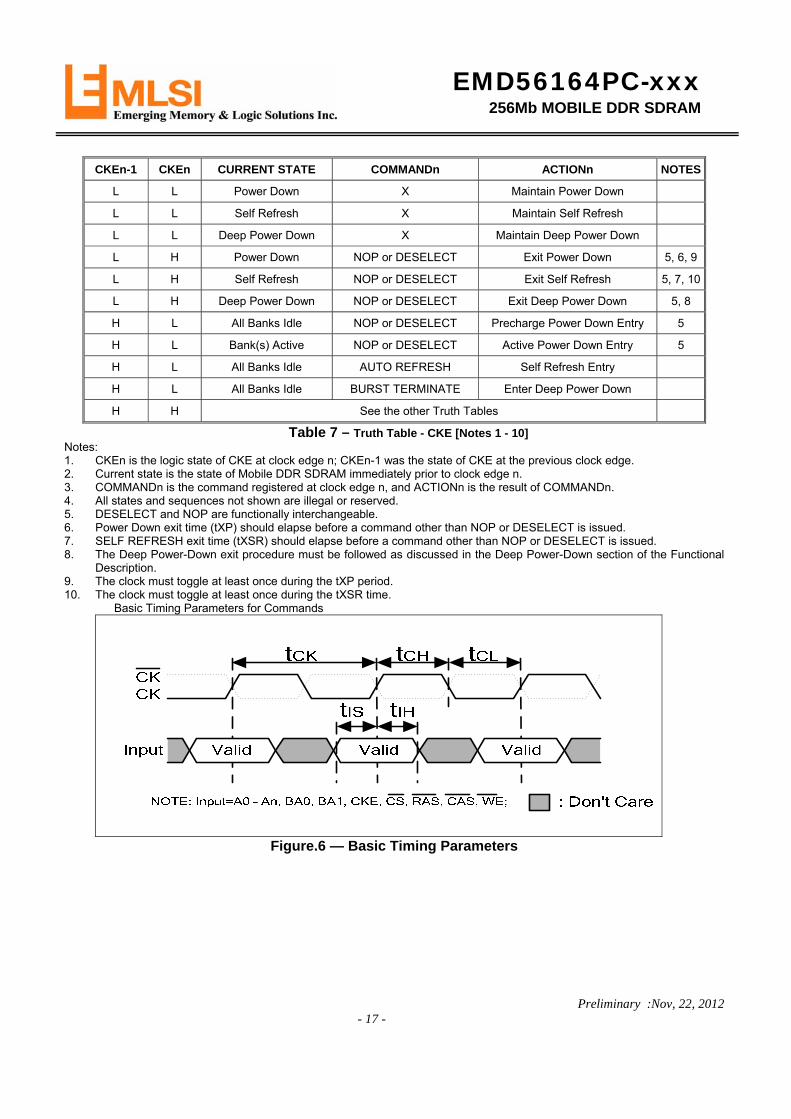
CKEn-1 CKEn CURRENT STATE COMMANDn ACTIONn NOTES
L L Power Down X Maintain Power Down
L L Self Refresh X Maintain Self Refresh
L L Deep Power Down X Maintain Deep Power Down
L H Power Down NOP or DESELECT Exit Power Down 5, 6, 9
L H Self Refresh NOP or DESELECT Exit Self Refresh 5, 7, 10
L H Deep Power Down NOP or DESELECT Exit Deep Power Down 5, 8
H L All Banks Idle NOP or DESELECT Precharge Power Down Entry 5
H L Bank(s) Active NOP or DESELECT Active Power Down Entry 5
H L All Banks Idle AUTO REFRESH Self Refresh Entry
H L All Banks Idle BURST TERMINATE Enter Deep Power Down
H H See the other Truth Tables
Table 7 – Truth Table - CKE [Notes 1 - 10] Notes: 1. CKEn is the logic state of CKE at clock edge n; CKEn-1 was the state of CKE at the previous clock edge. 2. Current state is the state of Mobile DDR SDRAM immediately prior to clock edge n. 3. COMMANDn is the command registered at clock edge n, and ACTIONn is the result of COMMANDn. 4. All states and sequences not shown are illegal or reserved. 5. DESELECT and NOP are functionally interchangeable. 6. Power Down exit time (tXP) should elapse before a command other than NOP or DESELECT is issued. 7. SELF REFRESH exit time (tXSR) should elapse before a command other than NOP or DESELECT is issued. 8. The Deep Power-Down exit procedure must be followed as discussed in the Deep Power-Down section of the Functional
Description. 9. The clock must toggle at least once during the tXP period. 10. The clock must toggle at least once during the tXSR time.
Basic Timing Parameters for Commands
Figure.6 — Basic Timing Parameters
EMD56164PC-xxx 256Mb MOBILE DDR SDRAM
Preliminary :Nov, 22, 2012 - 18 -
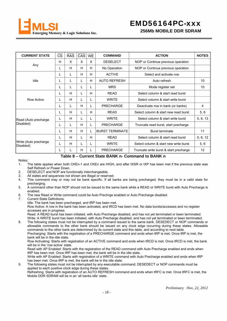
CURRENT STATE CS RAS CAS WE COMMAND ACTION NOTES
Any H X X X DESELECT NOP or Continue previous operation
L H H H No Operation NOP or Continue previous operation
Idle
L L H H ACTIVE Select and activate row
L L L H AUTO REFRESH Auto refresh 10
L L L L MRS Mode register set 10
Row Active
L H L H READ Select column & start read burst
L H L L WRITE Select column & start write burst
L L H L PRECHARGE Deactivate row in bank (or banks) 4
Read (Auto precharge Disabled)
L H L H READ Select column & start new read burst 5, 6
L H L L WRITE Select column & start write burst 5, 6, 13
L L H L PRECHARGE Truncate read burst, start precharge
L H H L BURST TERMINATE Burst terminate 11
Write (Auto precharge Disabled)
L H L H READ Select column & start read burst 5, 6, 12
L H L L WRITE Select column & start new write burst 5, 6
L L H L PRECHARGE Truncate write burst & start precharge 12
Table 8 – Current State BANK n- Command to BANK n Notes: 1. The table applies when both CKEn-1 and CKEn are HIGH, and after tXSR or tXP has been met if the previous state was
Self Refresh or Power Down. 2. DESELECT and NOP are functionally interchangeable. 3. All states and sequences not shown are illegal or reserved. 4. This command may or may not be bank specific. If all banks are being precharged, they must be in a valid state for
precharging. 5. A command other than NOP should not be issued to the same bank while a READ or WRITE burst with Auto Precharge is
enabled. 6. The new Read or Write command could be Auto Prechrge enabled or Auto Precharge disabled. 7. Current State Definitions:
Idle: The bank has been precharged, and tRP has been met. Row Active: A row in the bank has been activated, and tRCD has been met. No data bursts/accesses and no register accesses are in progress. Read: A READ burst has been initiated, with Auto Precharge disabled, and has not yet terminated or been terminated. Write: A WRITE burst has been initiated, with Auto Precharge disabled, and has not yet terminated or been terminated.
8. The following states must not be interrupted by a command issued to the same bank. DESEDECT or NOP commands or allowable commands to the other bank should be issued on any clock edge occurring during these states. Allowable commands to the other bank are determined by its current state and this table, and according to next table. Precharging: Starts with the registration of a PRECHARGE command and ends when tRP is met. Once tRP is met, the bank will be in the idle state. Row Activating: Starts with registration of an ACTIVE command and ends when tRCD is met. Once tRCD is met, the bank will be in the ‘row active’ state. Read with AP Enabled: Starts with the registration of the READ command with Auto Precharge enabled and ends when tRP has been met. Once tRP has been met, the bank will be in the idle state. Write with AP Enabled: Starts with registration of a WRITE command with Auto Precharge enabled and ends when tRP has been met. Once tRP is met, the bank will be in the idle state.
9. The following states must not be interrupted by any executable command; DESEDECT or NOP commands must be applied to each positive clock edge during these states. Refreshing: Starts with registration of an AUTO REFRESH command and ends when tRFC is met. Once tRFC is met, the Mobile DDR SDRAM will be in an ‘all banks idle’ state.

EMD56164PC-xxx 256Mb MOBILE DDR SDRAM
Preliminary :Nov, 22, 2012 - 19 -
Accessing Mode Register: Starts with registration of a MODE REGISTER SET command and ends when tMRD has been met. Once tMRD is met, the Mobile DDR SDRAM will be in an ‘all banks idle’ state. Precharging All: Starts with the registration of a PRECHARGE ALL command and ends when tRP is met. Once tRP is met, the bank will be in the idle state.
10. Not bank-specific; requires that all banks are idle and no bursts are in progress. 11. Not bank-specific. BURST TERMINATE affects the most recent READ burst, regardless of bank. 12. Requires appropriate DM masking. 13. A WRITE command may be applied after the completion of the READ burst; otherwise, a BURST TERMINATE must be
used to end the READ prior to asserting a WRITE command.
CURRENT STATE CS RAS CAS WE COMMAND ACTION NOTES
Any H X X X DESELECT NOP or Continue previous Operation
L H H H NOP NOP or Continue previous Operation
Idle X X X X ANY Any command allowed to bank m
Row Activating, Active, or
Precharging
L L H H ACTIVE Select and activate row
L H L H READ Select column & start read burst 8
L H L L WRITE Select column & start write burst 8
L L H L PRECHARGE Precharge
Read with Auto Precharge disabled
L L H H ACTIVE Select and activate row
L H L H READ Select column & start new read burst 8
L H L L WRITE Select column & start write burst 8,10
L L H L PRECHARGE Precharge
Write with Auto Precharge disabled
L L H H ACTIVE Select and activate row
L H L H READ Select column & start read burst 8, 9
L H L L WRITE Select column & start new write burst 8
L L H L PRECHARGE Precharge
Read with Auto Precharge
L L H H ACTIVE Select and activate row
L H L H READ Select column & start new read burst 5, 8
L H L L WRITE Select column & start write burst 5, 8, 10
L L H L PRECHARGE Precharge
Write with Auto Precharge
L L H H ACTIVE Select and activate row
L H L H READ Select column & start read burst 5, 8
L H L L WRITE Select column & start new write burst 5, 8
L L H L PRECHARGE Precharge
Table 9 – Current State BANK n- Command to BANK m
EMD56164PC-xxx 256Mb MOBILE DDR SDRAM
Preliminary :Nov, 22, 2012 - 20 -
Notes: 1. The table applies when both CKEn-1 and CKEn are HIGH, and after tXSR or tXP has been met if the previous state was
Self Refresh or Power Down. 2. DESELECT and NOP are functionally interchangeable. 3. All states and sequences not shown are illegal or reserved. 4. Current State Definitions:
Idle: The bank has been precharged, and tRP has been met. Row Active: A row in the bank has been activated, and tRCD has been met. No data bursts/accesses and no register accesses are in progress. Read: A READ burst has been initiated, with Auto Precharge disabled, and has not yet terminated or been terminated. Write: A Write burst has been initiated, with Auto Precharge disabled, and has not yet terminated or been terminated.
5. Read with AP enabled and Write with AP enabled: The read with Auto Precharge enabled or Write with Auto Precharge enabled states can be broken into two parts: the access period and the precharge period. For Read with AP, the precharge period is defined as if the same burst was executed with Auto Precharge disabled and then followed with the earliest possible PRECHARGE command that still accesses all the data in the burst. For Write with Auto precharge, the precharge period begins when tWR ends, with tWR measured as if Auto Precharge was disabled. The access period starts with registration of the command and ends where the precharge period (or tRP) begins. During the precharge period, of the Read with Auto Precharge enabled or Write with Auto Precharge enabled states, ACTIVE, PRECHARGE, READ, and WRITE commands to the other bank may be applied; during the access period, only ACTIVE and PRECHARGE commands to the other banks may be applied. In either case, all other related limitations apply (e.g. contention between READ data and WRITE data must be avoided).
6. AUTO REFRESH, SELF REFRESH, and MODE REGISTER SET commands may only be issued when all bank are idle. 7. A BURST TERMINATE command cannot be issued to another bank; it applies to the bank represented by the current
state only. 8. READs or WRITEs listed in the Command column include READs and WRITEs with Auto Precharge enabled and READs
and WRITEs with Auto Precharge disabled. 9. Requires appropriate DM masking. 10. A WRITE command may be applied after the completion of data output, otherwise a BURST TERMINATE command must
be issued to end the READ prior to asserting a WRITE command.
EMD56164PC-xxx 256Mb MOBILE DDR SDRAM
Preliminary :Nov, 22, 2012 - 21 -
7.OPERATION 7.1. Deselect The DESELECT function (/CS HIGH) prevents new commands from being executed by the Mobile DDR SDRAM. The Mobile DDR SDRAM is effectively deselected. Operations already in progress are not affected.
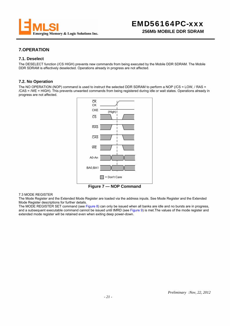
7.2. No Operation The NO OPERATION (NOP) command is used to instruct the selected DDR SDRAM to perform a NOP (/CS = LOW, / RAS = /CAS = /WE = HIGH). This prevents unwanted commands from being registered during idle or wait states. Operations already in progress are not affected.
= Don't Care
(High)
CKCK
CKE
CS
RAS
CAS
WE
A0-An
BA0,BA1
Figure 7 — NOP Command
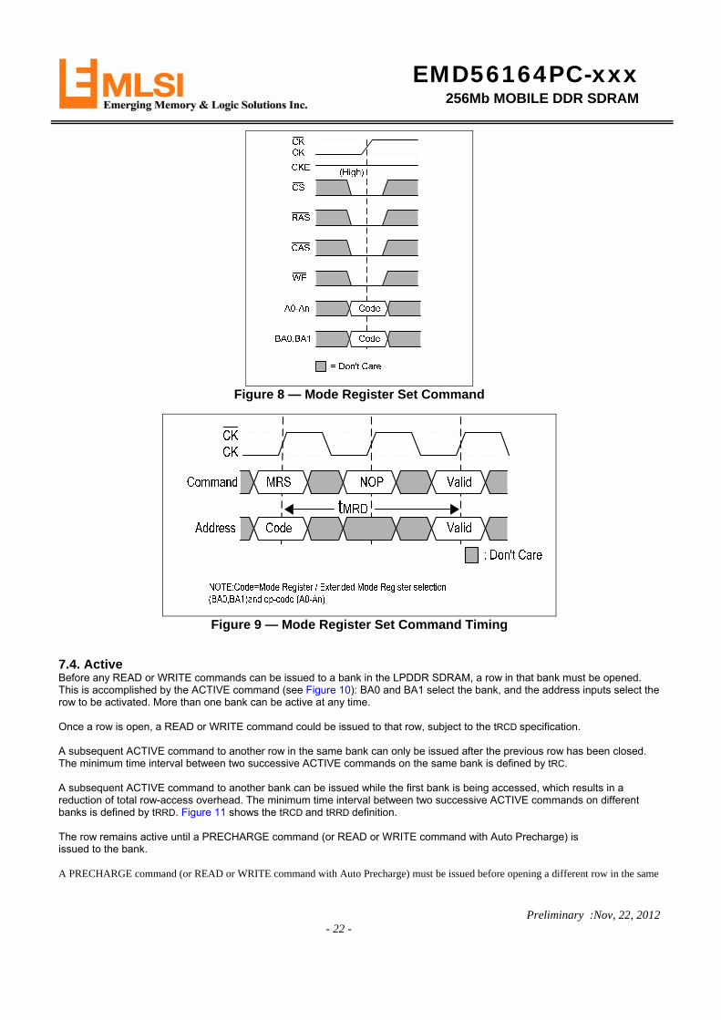
7.3 MODE REGISTER The Mode Register and the Extended Mode Register are loaded via the address inputs. See Mode Register and the Extended Mode Register descriptions for further details. The MODE REGISTER SET command (see Figure 8) can only be issued when all banks are idle and no bursts are in progress, and a subsequent executable command cannot be issued until tMRD (see Figure 9) is met.The values of the mode register and extended mode register will be retained even when exiting deep power-down.
EMD56164PC-xxx 256Mb MOBILE DDR SDRAM
Preliminary :Nov, 22, 2012 - 22 -
Figure 8 — Mode Register Set Command
Figure 9 — Mode Register Set Command Timing
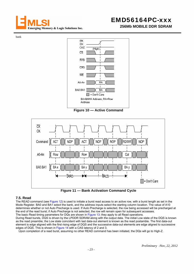
7.4. Active Before any READ or WRITE commands can be issued to a bank in the LPDDR SDRAM, a row in that bank must be opened. This is accomplished by the ACTIVE command (see Figure 10): BA0 and BA1 select the bank, and the address inputs select the row to be activated. More than one bank can be active at any time. Once a row is open, a READ or WRITE command could be issued to that row, subject to the tRCD specification. A subsequent ACTIVE command to another row in the same bank can only be issued after the previous row has been closed. The minimum time interval between two successive ACTIVE commands on the same bank is defined by tRC. A subsequent ACTIVE command to another bank can be issued while the first bank is being accessed, which results in a reduction of total row-access overhead. The minimum time interval between two successive ACTIVE commands on different banks is defined by tRRD. Figure 11 shows the tRCD and tRRD definition. The row remains active until a PRECHARGE command (or READ or WRITE command with Auto Precharge) is issued to the bank. A PRECHARGE command (or READ or WRITE command with Auto Precharge) must be issued before opening a different row in the same
EMD56164PC-xxx 256Mb MOBILE DDR SDRAM
Preliminary :Nov, 22, 2012 - 23 -
bank
Figure 10 — Active Command
Figure 11 — Bank Activation Command Cycle
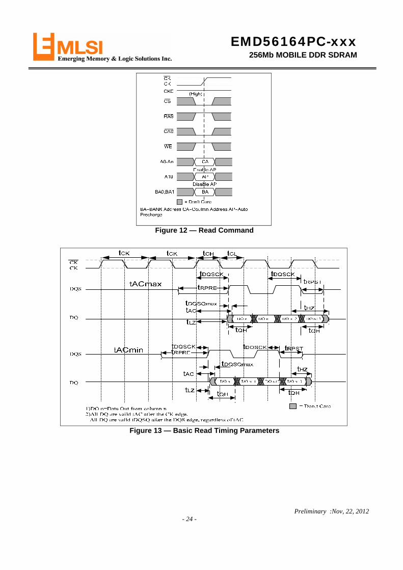
7.5. Read The READ command (see Figure 12) is used to initiate a burst read access to an active row, with a burst length as set in the Mode Register. BA0 and BA1 select the bank, and the address inputs select the starting column location. The value of A10 determines whether or not Auto Precharge is used. If Auto Precharge is selected, the row being accessed will be precharged at the end of the read burst; if Auto Precharge is not selected, the row will remain open for subsequent accesses. The basic Read timing parameters for DQs are shown in Figure 13; they apply to all Read operations. During Read bursts, DQS is driven by the LPDDR SDRAM along with the output data. The initial Low state of the DQS is known as the read preamble; the Low state coincident with last data-out element is known as the read postamble. The first data-out element is edge aligned with the first rising edge of DQS and the successive data-out elements are edge aligned to successive edges of DQS. This is shown in Figure 14 with a CAS latency of 2 and 3.
Upon completion of a read burst, assuming no other READ command has been initiated, the DQs will go to High-Z.
EMD56164PC-xxx 256Mb MOBILE DDR SDRAM
Preliminary :Nov, 22, 2012 - 24 -
Figure 12 — Read Command
Figure 13 — Basic Read Timing Parameters
EMD56164PC-xxx 256Mb MOBILE DDR SDRAM
Preliminary :Nov, 22, 2012 - 25 -
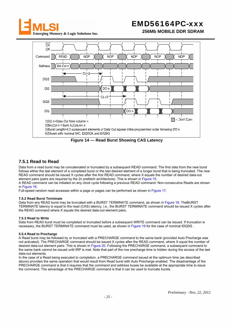
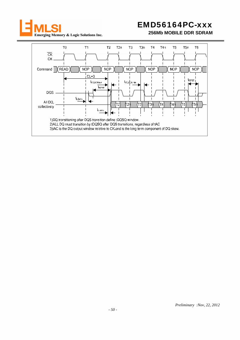
Figure 14 — Read Burst Showing CAS Latency
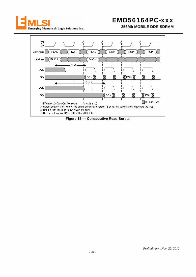
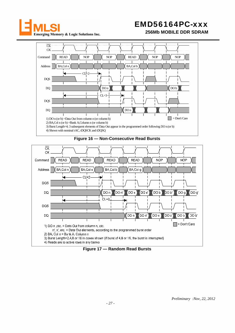
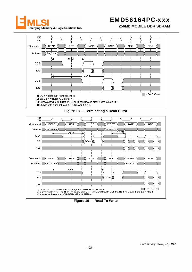
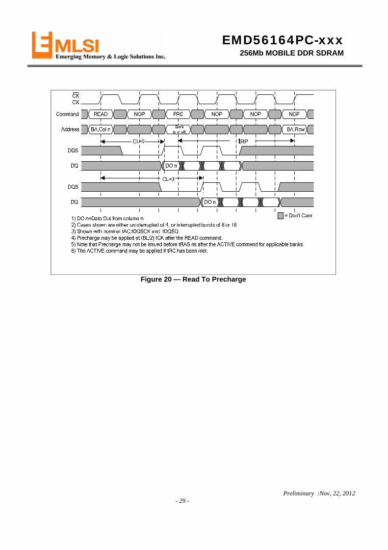
7.5.1 Read to Read Data from a read burst may be concatenated or truncated by a subsequent READ command. The first data from the new burst follows either the last element of a completed burst or the last desired element of a longer burst that is being truncated. The new READ command should be issued X cycles after the first READ command, where X equals the number of desired data-out element pairs (pairs are required by the 2n prefetch architecture). This is shown in Figure 15. A READ command can be initiated on any clock cycle following a previous READ command. Non-consecutive Reads are shown in Figure 16. Full-speed random read accesses within a page or pages can be performed as shown in Figure 17. 7.5.2 Read Burst Terminate Data from any READ burst may be truncated with a BURST TERMINATE command, as shown in Figure 18. TheBURST TERMINATE latency is equal to the read (CAS) latency, i.e., the BURST TERMINATE command should be issued X cycles after the READ command where X equals the desired data-out element pairs. 7.5.3 Read to Write Data from READ burst must be completed or truncated before a subsequent WRITE command can be issued. If truncation is necessary, the BURST TERMINATE command must be used, as shown in Figure 19 for the case of nominal tDQSS . 5.5.4 Read to Precharge A Read burst may be followed by or truncated with a PRECHARGE command to the same bank (provided Auto Precharge was not activated). The PRECHARGE command should be issued X cycles after the READ command, where X equal the number of desired data-out element pairs. This is shown in Figure 20. Following the PRECHARGE command, a subsequent command to the same bank cannot be issued until tRP is met. Note that part of the row precharge time is hidden during the access of the last data-out elements. In the case of a Read being executed to completion, a PRECHARGE command issued at the optimum time (as described above) provides the same operation that would result from Read burst with Auto Precharge enabled. The disadvantage of the PRECHARGE command is that it requires that the command and address buses be available at the appropriate time to issue the command. The advantage of the PRECHARGE command is that it can be used to truncate bursts.
EMD56164PC-xxx 256Mb MOBILE DDR SDRAM
Preliminary :Nov, 22, 2012 - 26 -
Figure 15 — Consecutive Read Bursts
EMD56164PC-xxx 256Mb MOBILE DDR SDRAM
Preliminary :Nov, 22, 2012 - 27 -
CL=2
DO n
DO n
= Don't Care
BA,Col n
READ NOP NOP READ NOP NOP
CKCK
Command
Address
DQS
DQ
DQS
DQ
1) DO n (or b) =Data Out from column n (or column b)2) BA,Col n (or b) =Bank A,Column n (or column b)3) Burst Length=4; 3 subsequent elements of Data Out appear in the programmed order following DO n (or b)4) Shown with nominal tAC, tDQSCK and tDQSQ
DO b
CL=3
BA,Col b
Figure 16 — Non-Consecutive Read Bursts
Figure 17 — Random Read Bursts
EMD56164PC-xxx 256Mb MOBILE DDR SDRAM
Preliminary :Nov, 22, 2012 - 28 -
. Figure 18 — Terminating a Read Burst
Figure 19 — Read To Write
EMD56164PC-xxx 256Mb MOBILE DDR SDRAM
Preliminary :Nov, 22, 2012 - 29 -
Figure 20 — Read To Precharge
EMD56164PC-xxx 256Mb MOBILE DDR SDRAM
Preliminary :Nov, 22, 2012 - 30 -
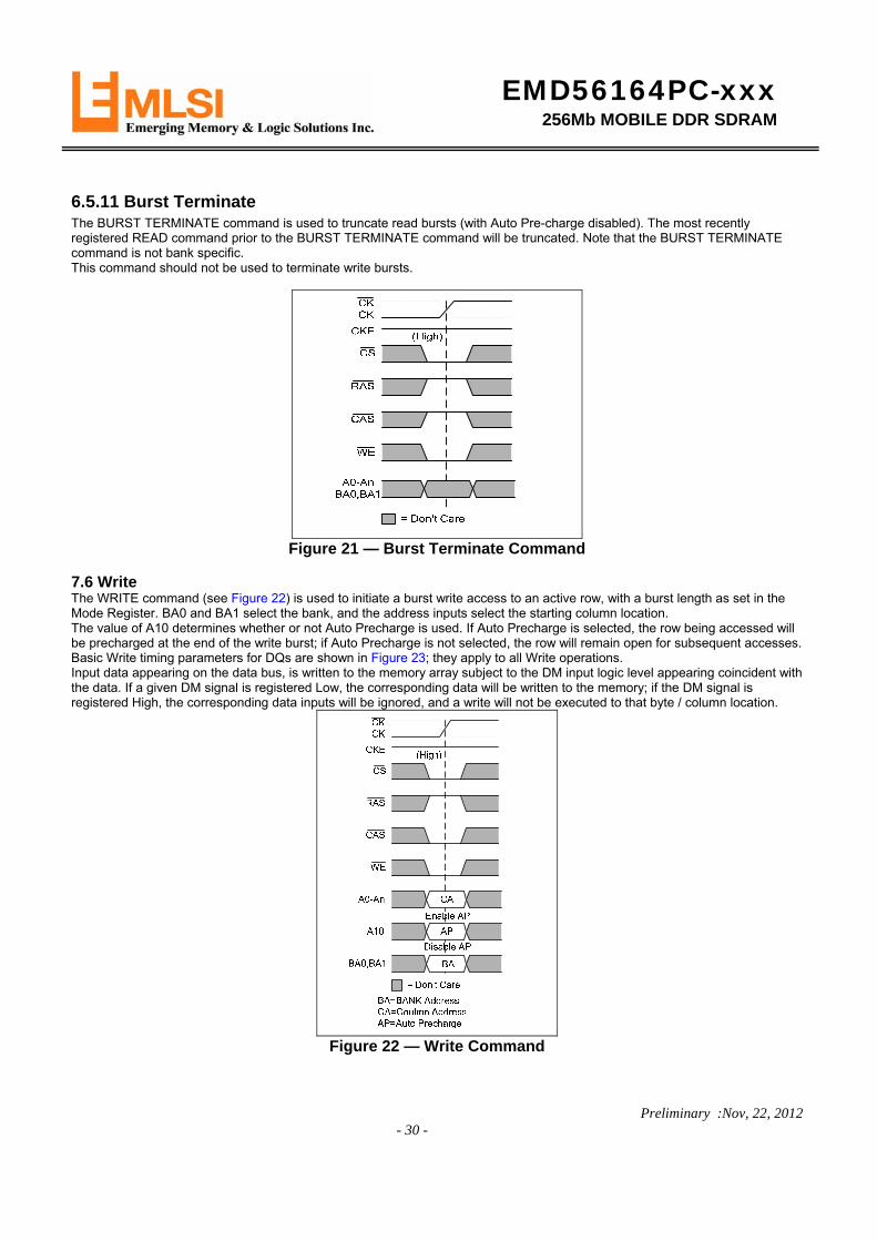
6.5.11 Burst Terminate The BURST TERMINATE command is used to truncate read bursts (with Auto Pre-charge disabled). The most recently registered READ command prior to the BURST TERMINATE command will be truncated. Note that the BURST TERMINATE command is not bank specific. This command should not be used to terminate write bursts.
Figure 21 — Burst Terminate Command
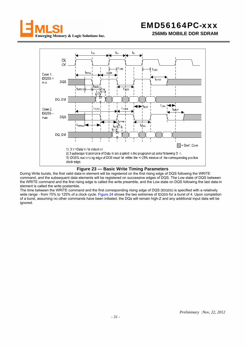
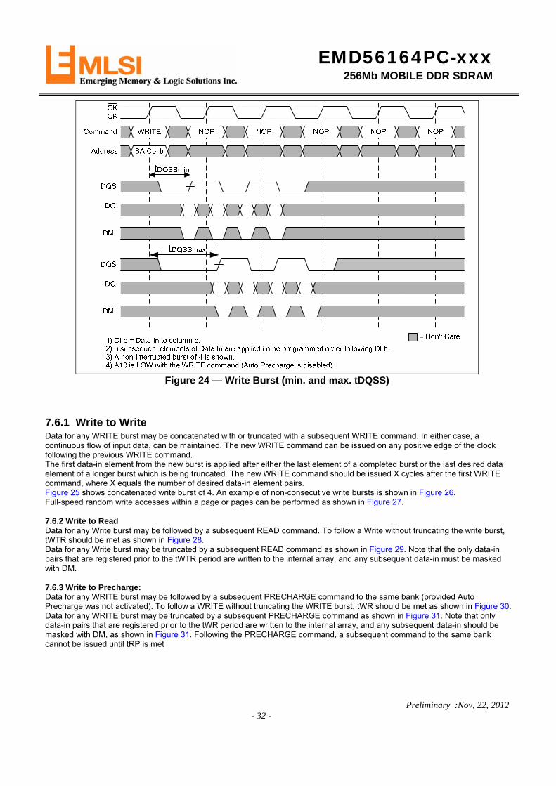
7.6 Write The WRITE command (see Figure 22) is used to initiate a burst write access to an active row, with a burst length as set in the Mode Register. BA0 and BA1 select the bank, and the address inputs select the starting column location. The value of A10 determines whether or not Auto Precharge is used. If Auto Precharge is selected, the row being accessed will be precharged at the end of the write burst; if Auto Precharge is not selected, the row will remain open for subsequent accesses. Basic Write timing parameters for DQs are shown in Figure 23; they apply to all Write operations. Input data appearing on the data bus, is written to the memory array subject to the DM input logic level appearing coincident with the data. If a given DM signal is registered Low, the corresponding data will be written to the memory; if the DM signal is registered High, the corresponding data inputs will be ignored, and a write will not be executed to that byte / column location.
Figure 22 — Write Command
EMD56164PC-xxx 256Mb MOBILE DDR SDRAM
Preliminary :Nov, 22, 2012 - 31 -
Figure 23 — Basic Write Timing Parameters
During Write bursts, the first valid data-in element will be registered on the first rising edge of DQS following the WRITE command, and the subsequent data elements will be registered on successive edges of DQS. The Low state of DQS between the WRITE command and the first rising edge is called the write preamble, and the Low state on DQS following the last data-in element is called the write postamble. The time between the WRITE command and the first corresponding rising edge of DQS (tDQSS) is specified with a relatively wide range - from 75% to 125% of a clock cycle. Figure 24 shows the two extremes of tDQSS for a burst of 4. Upon completion of a burst, assuming no other commands have been initiated, the DQs will remain high-Z and any additional input data will be ignored.
EMD56164PC-xxx 256Mb MOBILE DDR SDRAM
Preliminary :Nov, 22, 2012 - 32 -
Figure 24 — Write Burst (min. and max. tDQSS)
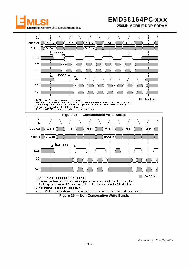
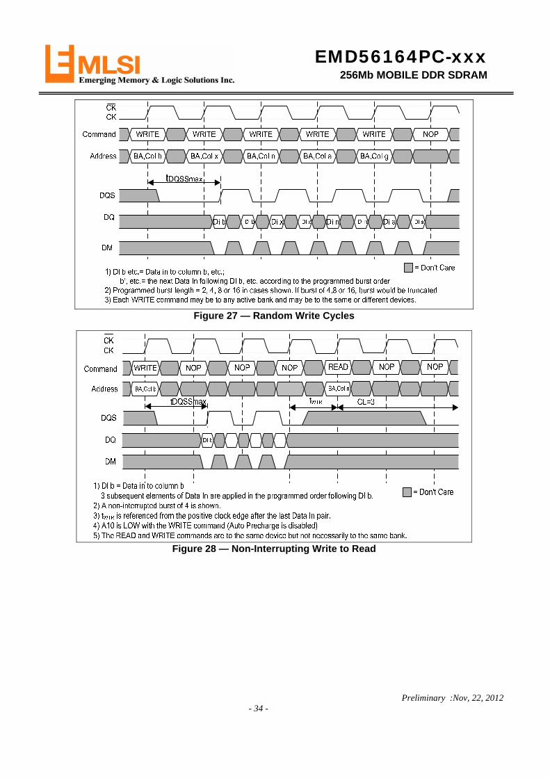
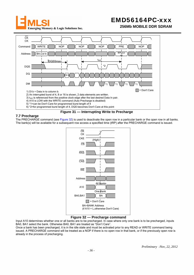
7.6.1 Write to Write Data for any WRITE burst may be concatenated with or truncated with a subsequent WRITE command. In either case, a continuous flow of input data, can be maintained. The new WRITE command can be issued on any positive edge of the clock following the previous WRITE command. The first data-in element from the new burst is applied after either the last element of a completed burst or the last desired data element of a longer burst which is being truncated. The new WRITE command should be issued X cycles after the first WRITE command, where X equals the number of desired data-in element pairs. Figure 25 shows concatenated write burst of 4. An example of non-consecutive write bursts is shown in Figure 26. Full-speed random write accesses within a page or pages can be performed as shown in Figure 27. 7.6.2 Write to Read Data for any Write burst may be followed by a subsequent READ command. To follow a Write without truncating the write burst, tWTR should be met as shown in Figure 28. Data for any Write burst may be truncated by a subsequent READ command as shown in Figure 29. Note that the only data-in pairs that are registered prior to the tWTR period are written to the internal array, and any subsequent data-in must be masked with DM. 7.6.3 Write to Precharge: Data for any WRITE burst may be followed by a subsequent PRECHARGE command to the same bank (provided Auto Precharge was not activated). To follow a WRITE without truncating the WRITE burst, tWR should be met as shown in Figure 30. Data for any WRITE burst may be truncated by a subsequent PRECHARGE command as shown in Figure 31. Note that only data-in pairs that are registered prior to the tWR period are written to the internal array, and any subsequent data-in should be masked with DM, as shown in Figure 31. Following the PRECHARGE command, a subsequent command to the same bank cannot be issued until tRP is met
EMD56164PC-xxx 256Mb MOBILE DDR SDRAM
Preliminary :Nov, 22, 2012 - 33 -
Figure 25 — Concatenated Write Bursts
Figure 26 — Non-Consecutive Write Bursts
EMD56164PC-xxx 256Mb MOBILE DDR SDRAM
Preliminary :Nov, 22, 2012 - 34 -
Figure 27 — Random Write Cycles
Figure 28 — Non-Interrupting Write to Read

EMD56164PC-xxx 256Mb MOBILE DDR SDRAM
Preliminary :Nov, 22, 2012 - 35 -
Figure 29 — Interrupting Write to Read
Figure 30 — Non-Interrupting Write to Precharge
EMD56164PC-xxx 256Mb MOBILE DDR SDRAM
Preliminary :Nov, 22, 2012 - 36 -
BA,Col n BA a(or all)
BA,Col b
WRITE PRE NOP
CKCK
Command
Address
1) Dl b = Data in to column b. 2) An interrupted burst of 4, 8 or 16 is shown, 2 data elements are written. 3) tWR is referenced from the positive clock edge after the last desired Data In pair.4) A10 is LOW with the WRITE command (Auto Precharge is disabled)5) *1=can be Don't Care for programmed burst length of 46) *2=for programmed burst length of 4, DQS becomes Don't Care at this point
NOP NOP NOP
= Don't Care
DQS
DQ
DM
tDQSSmaxtWR
DI b
*1*1*1*1
*2
Figure 31 — Interrupting Write to Precharge
7.7 Precharge The PRECHARGE command (see Figure 32) is used to deactivate the open row in a particular bank or the open row in all banks. The bank(s) will be available for a subsequent row access a specified time (tRP) after the PRECHARGE command is issued.
= Don't Care
(High)
CKCK
CKE
CS
RAS
CAS
WE
Address
BA=BANK Address(if A10 = L,otherwise Don't Care)
BABA0,BA1
A10All Banks
One Bank
Figure 32 — Precharge command
Input A10 determines whether one or all banks are to be precharged. In case where only one bank is to be precharged, inputs BA0, BA1 select the bank. Otherwise BA0, BA1 are treated as “Don’t Care”. Once a bank has been precharged, it is in the idle state and must be activated prior to any READ or WRITE command being issued. A PRECHARGE command will be treated as a NOP if there is no open row in that bank, or if the previously open row is already in the process of precharging.
EMD56164PC-xxx 256Mb MOBILE DDR SDRAM
Preliminary :Nov, 22, 2012 - 37 -
7.8 Auto Precharge Auto Precharge is a feature which performs the same individual bank precharge function as described above, but without requiring an explicit command. This is accomplished by using A10 (A10 = High), to enable Auto Precharge in conjunction with a specific READ or WRITE command. A precharge of the bank / row that is addressed with the READ or WRITE command is automatically performed upon completion of the read or write burst. Auto Precharge is non persistent in that it is either enabled or disabled for each individual READ or WRITE command. Auto Precharge ensures that a precharge is initiated at the earliest valid stage within a burst. The user must not issue another command to the same bank until the precharging time (tRP) is completed. This is determined as if an xplicit PRECHARGE command was issued at the earliest possible time, as described for each burst type in the Operation section of this specification. 7.9 Refresh Requirements LPDDR SDRAM devices require a refresh of all rows in any rolling 64ms interval. Each refresh is generated in one of two ways: by an explicit AUTO REFRESH command, or by an internally timed event in SELF REFRESH mode. Dividing the number of device rows into the rolling 64ms interval defines the average refresh interval (tREFI), which is a guideline to controllers for distributed refresh timing.
7.10 Auto Refresh AUTO REFRESH command (see Figure 33) is used during normal operation of the LPDDR SDRAM. This command is non persistent, so it must be issued each time a refresh is required.
= Don't Care
(High)
CKCK
CKE
CS
RAS
CAS
WE
A0-AnBA0,BA1
Figure 33 — Auto Refresh Command
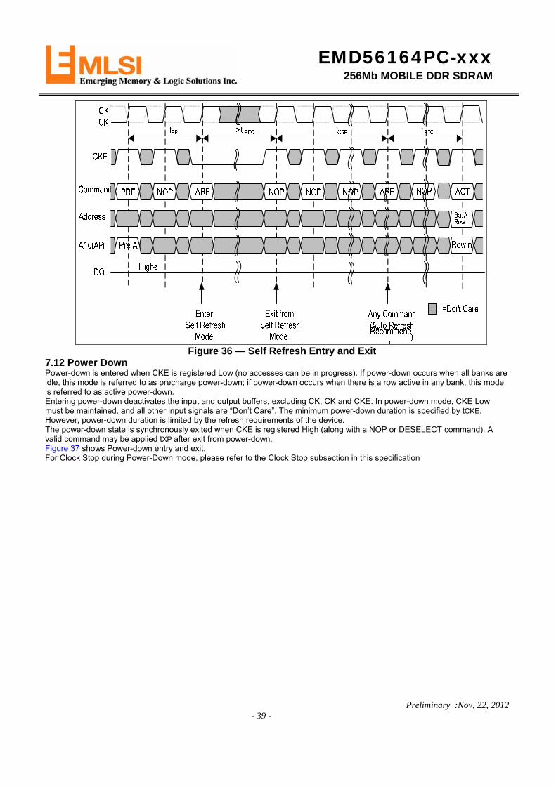
7.11 Self Referesh The SELF REFRESH command (see Figure 34) can be used to retain data in the LPDDR SDRAM, even if the rest of the system is powered down. When in the Self Refresh mode, the LPDDR SDRAM retains data without external clocking. The LPDDR SDRAM device has a built-in timer to accommodate Self Refresh operation. The SELF REFRESH command is initiated like an AUTO REFRESH command except CKE is LOW. Input signals except CKE are “Don’t Care” during Self Refresh. The user may halt the external clock one clock after the SELF REFRESH command is registered. Once the command is registered, CKE must be held low to keep the device in Self Refresh mode. The clock is internally disabled during Self Refresh operation to save power. The minimum time that the device must remain in Self Refresh mode is tRFC. The procedure for exiting Self Refresh requires a sequence of commands. First, the clock must be stable prior to CKE going back High. Once Self Refresh Exit is registered, a delay of at least tXS must be satisfied before a valid command can be issued to the device to allow for completion of any internal refresh in progress. The use of Self Refresh mode introduces the possibility that an internally timed refresh event can be missed when CKE is raised for exit from Self Refresh mode. Upon exit from Self Refresh an extra AUTO REFRESH command is recommended. Figure 36 shows Self Refresh entry and exit. In the Self Refresh mode, two additional power-saving options exist: Temperature Compensated Self Refresh (TCSR) and

EMD56164PC-xxx 256Mb MOBILE DDR SDRAM
Preliminary :Nov, 22, 2012 - 38 -
Partial Array Self Refresh (PASR); they are described in the Extended Mode Register section .
Figure 34 — Self Refresh command
Figure 35 — Auto Refresh Cycles Back-to-Back
EMD56164PC-xxx 256Mb MOBILE DDR SDRAM
Preliminary :Nov, 22, 2012 - 39 -
Figure 36 — Self Refresh Entry and Exit
7.12 Power Down Power-down is entered when CKE is registered Low (no accesses can be in progress). If power-down occurs when all banks are idle, this mode is referred to as precharge power-down; if power-down occurs when there is a row active in any bank, this mode is referred to as active power-down. Entering power-down deactivates the input and output buffers, excluding CK, CK and CKE. In power-down mode, CKE Low must be maintained, and all other input signals are “Don’t Care”. The minimum power-down duration is specified by tCKE. However, power-down duration is limited by the refresh requirements of the device. The power-down state is synchronously exited when CKE is registered High (along with a NOP or DESELECT command). A valid command may be applied tXP after exit from power-down. Figure 37 shows Power-down entry and exit. For Clock Stop during Power-Down mode, please refer to the Clock Stop subsection in this specification

EMD56164PC-xxx 256Mb MOBILE DDR SDRAM
Preliminary :Nov, 22, 2012 - 40 -
Figure 37 — Power-Down Entry and Exit
EMD56164PC-xxx 256Mb MOBILE DDR SDRAM
Preliminary :Nov, 22, 2012 - 41 -
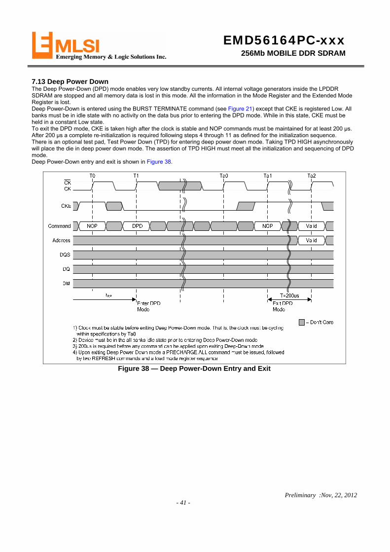
7.13 Deep Power Down The Deep Power-Down (DPD) mode enables very low standby currents. All internal voltage generators inside the LPDDR SDRAM are stopped and all memory data is lost in this mode. All the information in the Mode Register and the Extended Mode Register is lost. Deep Power-Down is entered using the BURST TERMINATE command (see Figure 21) except that CKE is registered Low. All banks must be in idle state with no activity on the data bus prior to entering the DPD mode. While in this state, CKE must be held in a constant Low state. To exit the DPD mode, CKE is taken high after the clock is stable and NOP commands must be maintained for at least 200 μs. After 200 μs a complete re-initialization is required following steps 4 through 11 as defined for the initialization sequence. There is an optional test pad, Test Power Down (TPD) for entering deep power down mode. Taking TPD HIGH asynchronously will place the die in deep power down mode. The assertion of TPD HIGH must meet all the initialization and sequencing of DPD mode. Deep Power-Down entry and exit is shown in Figure 38.
Figure 38 — Deep Power-Down Entry and Exit
EMD56164PC-xxx 256Mb MOBILE DDR SDRAM
Preliminary :Nov, 22, 2012 - 42 -
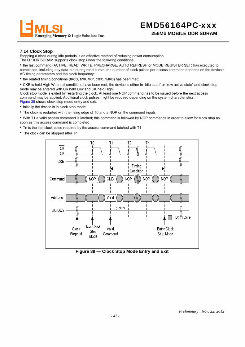
7.14 Clock Stop Stopping a clock during idle periods is an effective method of reducing power consumption. The LPDDR SDRAM supports clock stop under the following conditions:
• the last command (ACTIVE, READ, WRITE, PRECHARGE, AUTO REFRESH or MODE REGISTER SET) has executed to completion, including any data-out during read bursts; the number of clock pulses per access command depends on the device’s AC timing parameters and the clock frequency;
• the related timing conditions (tRCD, tWR, tRP, tRFC, tMRD) has been met;
• CKE is held High When all conditions have been met, the device is either in “idle state” or “row active state” and clock stop mode may be entered with CK held Low and CK held High. Clock stop mode is exited by restarting the clock. At least one NOP command has to be issued before the next access command may be applied. Additional clock pulses might be required depending on the system characteristics. Figure 39 shows clock stop mode entry and exit.
• Initially the device is in clock stop mode
• The clock is restarted with the rising edge of T0 and a NOP on the command inputs
• With T1 a valid access command is latched; this command is followed by NOP commands in order to allow for clock stop as soon as this access command is completed
• Tn is the last clock pulse required by the access command latched with T1
• The clock can be stopped after Tn
Figure 39 — Clock Stop Mode Entry and Exit
EMD56164PC-xxx 256Mb MOBILE DDR SDRAM
Preliminary :Nov, 22, 2012 - 43 -
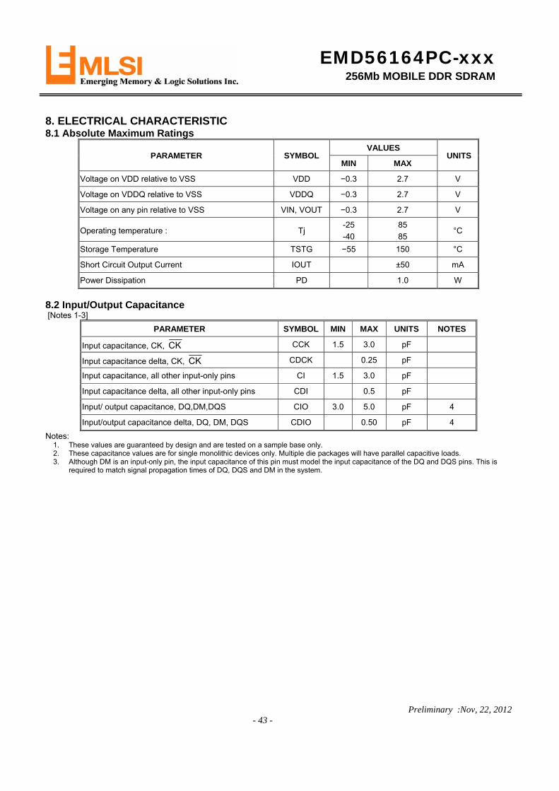
8. ELECTRICAL CHARACTERISTIC 8.1 Absolute Maximum Ratings
PARAMETER SYMBOL VALUES
UNITS MIN MAX
Voltage on VDD relative to VSS VDD −0.3 2.7 V
Voltage on VDDQ relative to VSS VDDQ −0.3 2.7 V
Voltage on any pin relative to VSS VIN, VOUT −0.3 2.7 V
Operating temperature : Tj -25
-40
85
85 °C
Storage Temperature TSTG −55 150 °C
Short Circuit Output Current IOUT ±50 mA
Power Dissipation PD 1.0 W
8.2 Input/Output Capacitance [Notes 1-3]
PARAMETER SYMBOL MIN MAX UNITS NOTES
Input capacitance, CK, CK CCK 1.5 3.0 pF
Input capacitance delta, CK, CK CDCK 0.25 pF
Input capacitance, all other input-only pins CI 1.5 3.0 pF
Input capacitance delta, all other input-only pins CDI 0.5 pF
Input/ output capacitance, DQ,DM,DQS CIO 3.0 5.0 pF 4
Input/output capacitance delta, DQ, DM, DQS CDIO 0.50 pF 4
Notes: 1. These values are guaranteed by design and are tested on a sample base only. 2. These capacitance values are for single monolithic devices only. Multiple die packages will have parallel capacitive loads. 3. Although DM is an input-only pin, the input capacitance of this pin must model the input capacitance of the DQ and DQS pins. This is
required to match signal propagation times of DQ, DQS and DM in the system.
EMD56164PC-xxx 256Mb MOBILE DDR SDRAM
Preliminary :Nov, 22, 2012 - 44 -
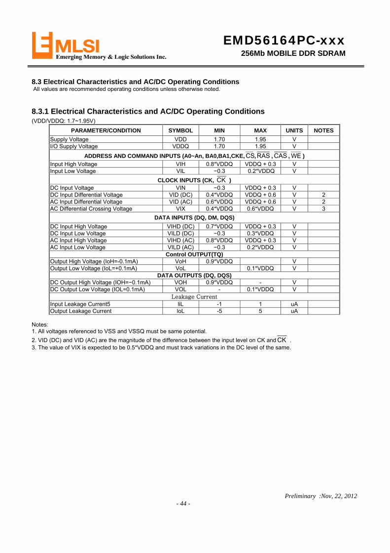
8.3 Electrical Characteristics and AC/DC Operating Conditions All values are recommended operating conditions unless otherwise noted.
8.3.1 Electrical Characteristics and AC/DC Operating Conditions (VDD/VDDQ: 1.7~1.95V)
PARAMETER/CONDITION SYMBOL MIN MAX UNITS NOTES
Supply Voltage VDD 1.70 1.95 V I/O Supply Voltage VDDQ 1.70 1.95 V
ADDRESS AND COMMAND INPUTS (A0~An, BA0,BA1,CKE, CS, RAS , CAS , WE )
Input High Voltage VIH 0.8*VDDQ VDDQ + 0.3 V Input Low Voltage VIL −0.3 0.2*VDDQ V
CLOCK INPUTS (CK, CK ) DC Input Voltage VIN −0.3 VDDQ + 0.3 V DC Input Differential Voltage VID (DC) 0.4*VDDQ VDDQ + 0.6 V 2 AC Input Differential Voltage VID (AC) 0.6*VDDQ VDDQ + 0.6 V 2 AC Differential Crossing Voltage VIX 0.4*VDDQ 0.6*VDDQ V 3
DATA INPUTS (DQ, DM, DQS)
DC Input High Voltage VIHD (DC) 0.7*VDDQ VDDQ + 0.3 V DC Input Low Voltage VILD (DC) −0.3 0.3*VDDQ V AC Input High Voltage VIHD (AC) 0.8*VDDQ VDDQ + 0.3 V AC Input Low Voltage VILD (AC) −0.3 0.2*VDDQ V
Control OUTPUT(TQ) Output High Voltage (IoH=-0.1mA) VoH 0.9*VDDQ V Output Low Voltage (IoL=+0.1mA) VoL 0.1*VDDQ V
DATA OUTPUTS (DQ, DQS) DC Output High Voltage (IOH=−0.1mA) VOH 0.9*VDDQ - V DC Output Low Voltage (IOL=0.1mA) VOL - 0.1*VDDQ V
Leakage Current Input Leakage Current5 liL -1 1 uA Output Leakage Current loL -5 5 uA
Notes: 1. All voltages referenced to VSS and VSSQ must be same potential.
2. VID (DC) and VID (AC) are the magnitude of the difference between the input level on CK and CK . 3. The value of VIX is expected to be 0.5*VDDQ and must track variations in the DC level of the same.
EMD56164PC-xxx 256Mb MOBILE DDR SDRAM
Preliminary :Nov, 22, 2012 - 45 -
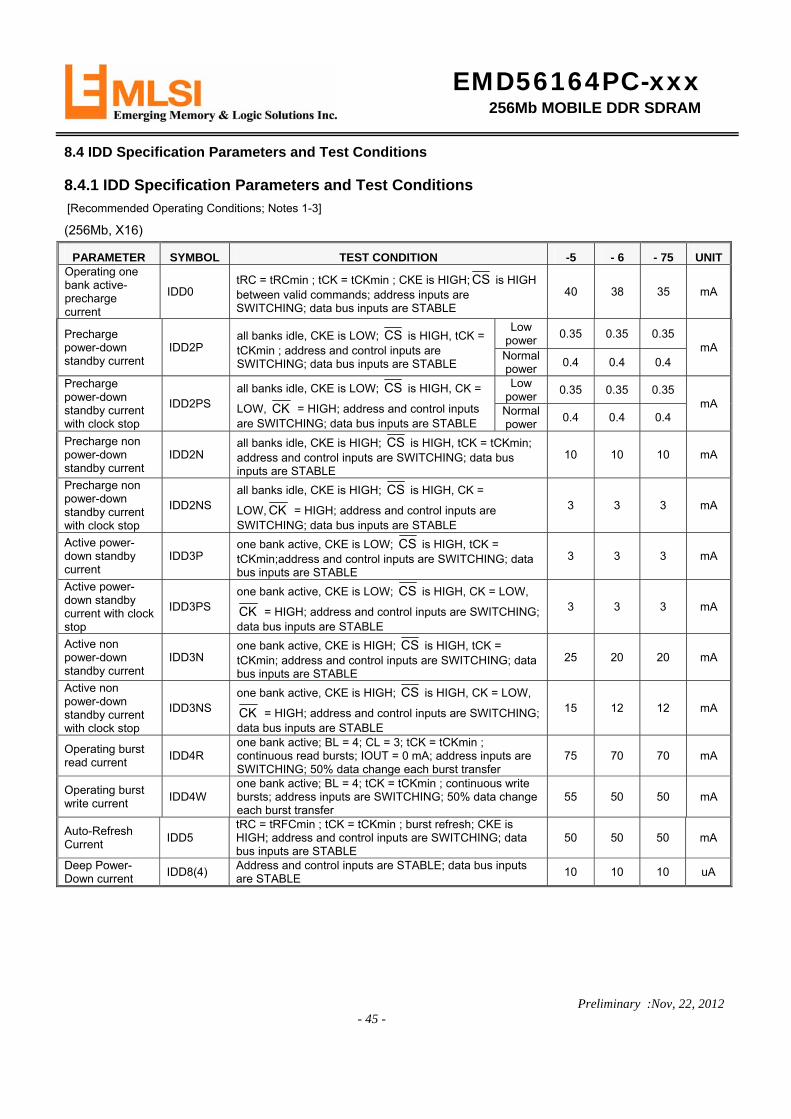
8.4 IDD Specification Parameters and Test Conditions
8.4.1 IDD Specification Parameters and Test Conditions
[Recommended Operating Conditions; Notes 1-3]
(256Mb, X16)
PARAMETER SYMBOL TEST CONDITION -5 - 6 - 75 UNITOperating one bank active-precharge current
IDD0 tRC = tRCmin ; tCK = tCKmin ; CKE is HIGH; CS is HIGH between valid commands; address inputs are SWITCHING; data bus inputs are STABLE
40 38 35 mA
Precharge power-down standby current
IDD2P all banks idle, CKE is LOW; CS is HIGH, tCK = tCKmin ; address and control inputs are SWITCHING; data bus inputs are STABLE
Low power
0.35 0.35 0.35 mA
Normal power
0.4 0.4 0.4
Precharge power-down standby current with clock stop
IDD2PS all banks idle, CKE is LOW; CS is HIGH, CK =
LOW, CK = HIGH; address and control inputs are SWITCHING; data bus inputs are STABLE
Low power
0.35 0.35 0.35 mA
Normal power
0.4 0.4 0.4
Precharge non power-down standby current
IDD2N all banks idle, CKE is HIGH; CS is HIGH, tCK = tCKmin; address and control inputs are SWITCHING; data bus inputs are STABLE
10 10 10 mA
Precharge non power-down standby current with clock stop
IDD2NS all banks idle, CKE is HIGH; CS is HIGH, CK =
LOW, CK = HIGH; address and control inputs are SWITCHING; data bus inputs are STABLE
3 3 3 mA
Active power-down standby current
IDD3P one bank active, CKE is LOW; CS is HIGH, tCK = tCKmin;address and control inputs are SWITCHING; data bus inputs are STABLE
3 3 3 mA
Active power-down standby current with clock stop
IDD3PS one bank active, CKE is LOW; CS is HIGH, CK = LOW,
CK = HIGH; address and control inputs are SWITCHING; data bus inputs are STABLE
3 3 3 mA
Active non power-down standby current
IDD3N one bank active, CKE is HIGH; CS is HIGH, tCK = tCKmin; address and control inputs are SWITCHING; data bus inputs are STABLE
25 20 20 mA
Active non power-down standby current with clock stop
IDD3NS one bank active, CKE is HIGH; CS is HIGH, CK = LOW,
CK = HIGH; address and control inputs are SWITCHING; data bus inputs are STABLE
15 12 12 mA
Operating burst read current
IDD4R one bank active; BL = 4; CL = 3; tCK = tCKmin ; continuous read bursts; IOUT = 0 mA; address inputs are SWITCHING; 50% data change each burst transfer
75 70 70 mA
Operating burst write current
IDD4W one bank active; BL = 4; tCK = tCKmin ; continuous write bursts; address inputs are SWITCHING; 50% data change each burst transfer
55 50 50 mA
Auto-Refresh Current
IDD5 tRC = tRFCmin ; tCK = tCKmin ; burst refresh; CKE is HIGH; address and control inputs are SWITCHING; data bus inputs are STABLE
50 50 50 mA
Deep Power-Down current
IDD8(4) Address and control inputs are STABLE; data bus inputs are STABLE
10 10 10 uA
EMD56164PC-xxx 256Mb MOBILE DDR SDRAM
Preliminary :Nov, 22, 2012 - 46 -
Notes:
1. IDD specifications are tested after the device is properly initialized. 2. Input slew rate is 1V/ns. 3. Definitions for IDD:
LOW is defined as VIN ≤ 0.1 * VDDQ; HIGH is defined as VIN ≥ 0.9 * VDDQ; STABLE is defined as inputs stable at a HIGH or LOW level; SWITCHING is defined as: - Address and command: inputs changing between HIGH and LOW once per two clock cycles; - Data bus inputs: DQ changing between HIGH and LOW once per clock cycle; DM and DQS are STABLE.
4. IDD8 is a typical value at 25℃.
IDD6 Conditions :
IDD6 Low Power Normal Power Units
TCSR Range 45℃ 85℃ 45℃ 85℃
uA Full Array 200 350 250 400 1/2 Array 170 250 200 300 1/4 Array 150 220 180 250
Notes: 1. Measured with outputs open. 2. Internal TCSR can be supported.
EMD56164PC-xxx 256Mb MOBILE DDR SDRAM
Preliminary :Nov, 22, 2012 - 47 -
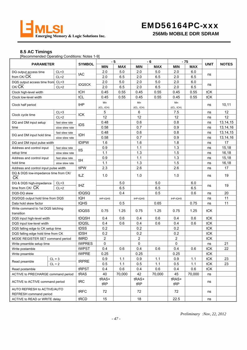
8.5 AC Timings [Recommended Operating Conditions: Notes 1-9]
PARAMETER SYMBOL - 5 - 6 - 75
UNIT NOTESMIN MAX MIN MAX MIN MAX
DQ output access time
from CK/ CK
CL=3 tAC
2.0 5.0 2.0 5.0 2.0 6.0 ns
CL=2 2.0 6.5 2.0 6.5 2.0 6.5
DQS output access time from
CK/ CK
CL=3 tDQSCK
2.0 5.0 2.0 5.0 2.0 6.0 ns
CL=2 2.0 6.5 2.0 6.5 2.0 6.5 Clock high-level width tCH 0.45 0.55 0.45 0.55 0.45 0.55 tCK Clock low-level width tCL 0.45 0.55 0.45 0.55 0.45 0.55 tCK
Clock half period tHP Min
(tCL, tCH)
Min
(tCL, tCH)
Min
(tCL, tCH) ns 10,11
Clock cycle time CL=3
tCK 5 6 7.5 ns 12
CL=2 12 12 12 ns 12
DQ and DM input setup
time
fast slew rate tDS
0.48 0.6 0.8 ns 13,14,15slow slew rate 0.58 0.7 0.9 ns 13,14,16
DQ and DM input hold time fast slew rate
tDH 0.48 0.6 0.8 ns 13,14,15
slow slew rate 0.58 0.7 0.9 ns 13,14,16
DQ and DM input pulse width tDIPW 1.6 1.6 1.8 ns 17
Address and control input
setup time
fast slew rate tIS
0.9 1.1 1.3 ns 15,18 slow slew rate 1.1 1.3 1.5 ns 16,18
Address and control input
hold time
fast slew rate tIH
0.9 1.1 1.3 ns 15,18
slow slew rate 1.1 1.3 1.5 ns 16,18 Address and control input pulse width tIPW 2.3 2.6 2.6 ns 17 DQ & DQS low-impedance time from CK/
CK tLZ 1.0 1.0 1.0 ns 19
DQ & DQS high-impedance
time from CK/ CK
CL=3 tHZ
5.0 5.0 6.0 ns 19
CL=2 6.5 6.5 6.5 DQS-DQ skew tDQSQ 0.4 0.5 0.6 ns 20
DQ/DQS output hold time from DQS tQH tHP-tQHS tHP-tQHS tHP-tQHS ns 11 Data hold skew factor tQHS 0.5 0.65 0.75 ns 11 Write command to 1st DQS latching
transition tDQSS 0.75 1.25 0.75 1.25 0.75 1.25 tCK
DQS input high-level width tDQSH 0.4 0.6 0.4 0.6 0.4 0.6 tCK DQS input low-level width tDQSL 0.4 0.6 0.4 0.6 0.4 0.6 tCK DQS falling edge to CK setup time tDSS 0.2 0.2 0.2 tCK
DQS falling edge hold time from CK tDSH 0.2 0.2 0.2 tCK MODE REGISTER SET command period tMRD 2 2 2 tCK Write preamble setup time tWPRES 0 0 0 ns 21 Write postamble tWPST 0.4 0.6 0.4 0.6 0.4 0.6 tCK 22
Write preamble tWPRE 0.25 0.25 0.25 tCK
Read preamble CL = 3
tRPRE 0.9 1.1 0.9 1.1 0.9 1.1 tCK 23
CL = 2 0.5 1.1 0.5 1.1 0.5 1.1 tCK 23 Read postamble tRPST 0.4 0.6 0.4 0.6 0.4 0.6 tCK
ACTIVE to PRECHARGE command period tRAS 40 70,000 42 70,000 45 70,000 ns
ACTIVE to ACTIVE command period tRC tRAS+
tRP
tRAS+tRP
tRAS+
tRP ns
AUTO REFRESH to ACTIVE/AUTO
REFRESH command period tRFC 72 72 72 ns
ACTIVE to READ or WRITE delay tRCD 15 18 22.5 ns
EMD56164PC-xxx 256Mb MOBILE DDR SDRAM
Preliminary :Nov, 22, 2012 - 48 -
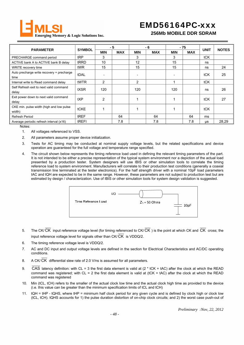
PARAMETER SYMBOL - 5 - 6 - 75
UNIT NOTESMIN MAX MIN MAX MIN MAX
PRECHARGE command period tRP 3 3 3 tCK
ACTIVE bank A to ACTIVE bank B delay tRRD 10 12 15 ns WRITE recovery time tWR 15 15 15 ns 24 Auto precharge write recovery + precharge
time tDAL - - - tCK 25
Internal write to Read command delay tWTR 2 2 1 tCK Self Refresh exit to next valid command
delay tXSR 120 120 120 ns 26
Exit power down to next valid command
delay tXP 2 1 1 tCK 27
CKE min. pulse width (high and low pulse
width) tCKE 1 1 1 tCK
Refresh Period tREF 64 64 64 ms
Average periodic refresh interval (x16) tREFI 7.8 7.8 7.8 μs 28,29 Notes:
1. All voltages referenced to VSS.
2. All parameters assume proper device initialization.
3. Tests for AC timing may be conducted at nominal supply voltage levels, but the related specifications and device operation are guaranteed for the full voltage and temperature range specified.
4. The circuit shown below represents the timing reference load used in defining the relevant timing parameters of the part. It is not intended to be either a precise representation of the typical system environment nor a depiction of the actual load presented by a production tester. System designers will use IBIS or other simulation tools to correlate the timing reference load to system environment. Manufacturers will correlate to their production test conditions (generally a coaxial transmission line terminated at the tester electronics). For the half strength driver with a nominal 10pF load parameters tAC and tQH are expected to be in the same range. However, these parameters are not subject to production test but are estimated by design / characterization. Use of IBIS or other simulation tools for system design validation is suggested.
5. The CK/ CK input reference voltage level (for timing referenced to CK/ CK ) is the point at which CK and CK cross; the
input reference voltage level for signals other than CK/ CK is VDDQ/2.
6. The timing reference voltage level is VDDQ/2.
7. AC and DC input and output voltage levels are defined in the section for Electrical Characteristics and AC/DC operating conditions.
8. A CK/ CK differential slew rate of 2.0 V/ns is assumed for all parameters.
9. CAS latency definition: with CL = 3 the first data element is valid at (2 * tCK + tAC) after the clock at which the READ command was registered; with CL = 2 the first data element is valid at (tCK + tAC) after the clock at which the READ command was registered
10. Min (tCL, tCH) refers to the smaller of the actual clock low time and the actual clock high time as provided to the device (i.e. this value can be greater than the minimum specification limits of tCL and tCH)
11. tQH = tHP - tQHS, where tHP = minimum half clock period for any given cycle and is defined by clock high or clock low (tCL, tCH). tQHS accounts for 1) the pulse duration distortion of on-chip clock circuits; and 2) the worst case push-out of
EMD56164PC-xxx 256Mb MOBILE DDR SDRAM
Preliminary :Nov, 22, 2012 - 49 -
DQS on one transition followed by the worst case pull-in of DQ on the next transition, both of which are, separately, due to data pin skew and output pattern effects, and p-channel to n-channel variation of the output drivers.
12. The only time that the clock frequency is allowed to change is during clock stop, power-down or self-refresh modes.
13. The transition time for DQ, DM and DQS inputs is measured between VIL(DC) to VIH(AC) for rising input signals, and VIH(DC) to VIL(AC) for falling input signals.
14. DQS, DM and DQ input slew rate is specified to prevent double clocking of data and preserve setup and hold times. Signal transitions through the DC region must be monotonic.
15. Input slew rate ≥ 1.0 V/ns.
16. Input slew rate ≥ 0.5 V/ns and < 1.0 V/ns.
17. These parameters guarantee device timing but they are not necessarily tested on each device.
18. The transition time for address and command inputs is measured between VIH and VIL.
19. tHZ and tLZ transitions occur in the same access time windows as valid data transitions. These parameters are not referred to a specific voltage level, but specify when the device is no longer driving (HZ), or begins driving (LZ).
20. tDQSQ consists of data pin skew and output pattern effects, and p-channel to n-channel variation of the output drivers for any given cycle.
21. The specific requirement is that DQS be valid (HIGH, LOW, or some point on a valid transition) on or before the corresponding CK edge. A valid transition is defined as monotonic and meeting the input slew rate specifications of the device. When no writes were previously in progress on the bus, DQS will be transitioning from Hi-Z to logic LOW. If a previous write was in progress, DQS could be HIGH, LOW, or transitioning from HIGH to LOW at this time, depending on tDQSS.
22. The maximum limit for this parameter is not a device limit. The device operates with a greater value for this parameter, but system performance (bus turnaround) will degrade accordingly.
23. A low level on DQS may be maintained during High-Z states (DQS drivers disabled) by adding a weak pull-down element in the system. It is recommended to turn off the weak pull-down element during read and write bursts (DQS drivers enabled).
24. At least one clock cycle is required during tWR time when in auto precharge mode.
25. Minimum 3 clocks of tDAL (=tWR + tRP) is required because it need minimum 2 clocks for tWR and minimum 1 clock for tRP.
tDAL = (tWR/tCK) + (tRP/tCK): for each of the terms above, if not already an integer, round to the next higher integer.
26. There must be at least two clock pulses during the tXSR period.
27. There must be at least one clock pulse during the tXP period.
28. tREFI values are dependence on density and bus width.
29. A maximum of 8 Refresh commands can be posted to any given M, meaning that the maximum absolute interval between any Refresh command and the next Refresh command is 8*tREFI.
CAS Latency Definition (With CL=3)
EMD56164PC-xxx 256Mb MOBILE DDR SDRAM
Preliminary :Nov, 22, 2012 - 50 -
EMD56164PC-xxx 256Mb MOBILE DDR SDRAM
Preliminary :Nov, 22, 2012 - 51 -
8.5.2 Output Slew Rate Characteristics PARAMETER MIN MAX UNIT NOTES
Pull-up and Pull-Down Slew Rate for Full Strength Driver 0.7 2.5 V/ns 1,2 Pull-up and Pull-Down Slew Rate for Three-Quarter Strength Driver 0.5 1.75 V/ns 1,2 Pull-up and Pull-Down Slew Rate for Half Strength Driver 0.3 1.0 V/ns 1,2 Output Slew rate Matching ratio (Pull-up to Pull-down) 0.7 1.4 - 3
Notes: 1. Measured with a test load of 20 pF connected to VSSQ. 2. Output slew rate for rising edge is measured between VILD(DC) to VIHD(AC) and for falling edge between VIHD(DC) to VILD(AC). 3. The ratio of pull-up slew rate to pull-down slew rate is specified for the same temperature and voltage, over the entire temperature and
voltage range. For a given output, it represents the maximum difference between pull-up and pull-down drivers due to process variation.
8.5.3 AC Overshoot/Undershoot Specification PARAMETER SPECIFICATION
Maximum peak amplitude allowed for overshoot 0.5 V Maximum peak amplitude allowed for undershoot 0.5 V The area between overshoot signal and VDD must be less than or equal to 3 V-ns The area between undershoot signal and GND must be less than or equal to 3 V-ns
EMD56164PC-xxx 256Mb MOBILE DDR SDRAM
Preliminary :Nov, 22, 2012 - 52 -
8.5.4 AC Overshoot and Undershoot Definition
Figure 40 — AC Overshoot and Undershoot Definition
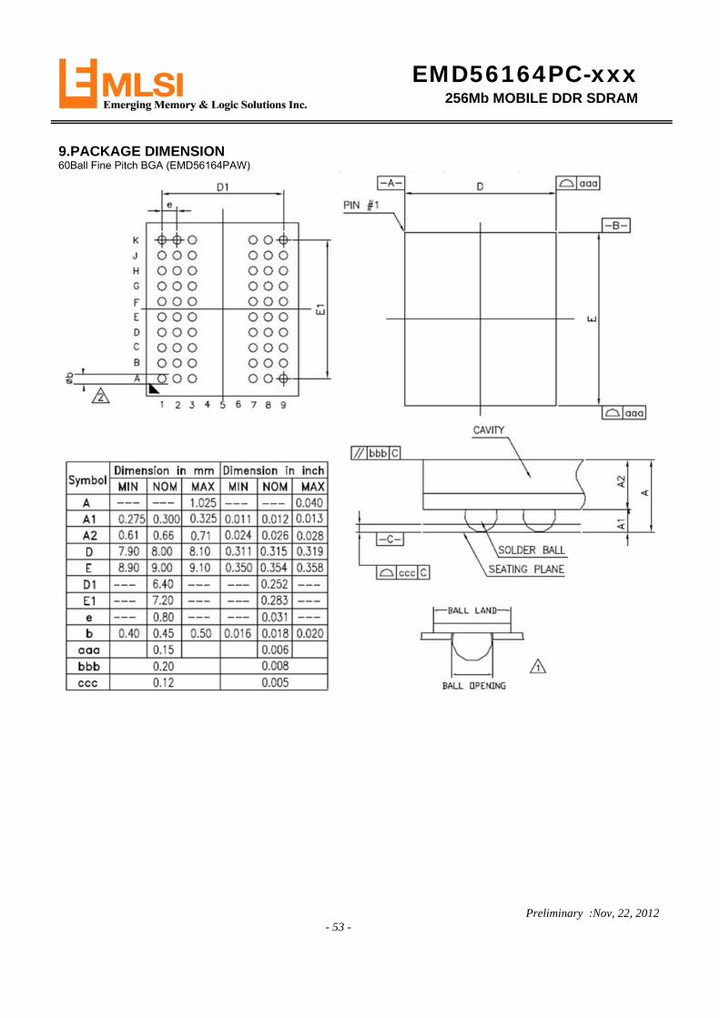
EMD56164PC-xxx 256Mb MOBILE DDR SDRAM
Preliminary :Nov, 22, 2012 - 53 -
9.PACKAGE DIMENSION 60Ball Fine Pitch BGA (EMD56164PAW)
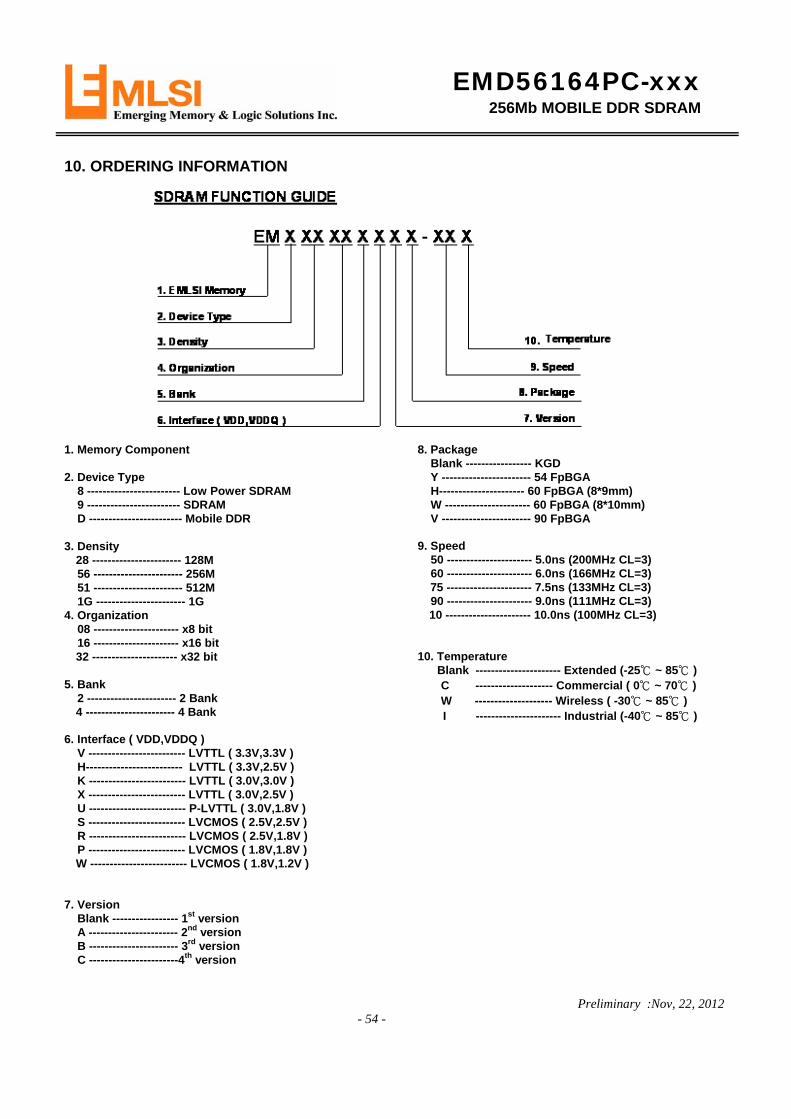
EMD56164PC-xxx 256Mb MOBILE DDR SDRAM
Preliminary :Nov, 22, 2012 - 54 -
10. ORDERING INFORMATION
1. Memory Component 2. Device Type 8 ------------------------ Low Power SDRAM 9 ------------------------ SDRAM D ------------------------ Mobile DDR 3. Density
28 ----------------------- 128M 56 ----------------------- 256M 51 ----------------------- 512M 1G ----------------------- 1G 4. Organization 08 ---------------------- x8 bit 16 ---------------------- x16 bit
32 ---------------------- x32 bit 5. Bank 2 ----------------------- 2 Bank
4 ----------------------- 4 Bank 6. Interface ( VDD,VDDQ ) V ------------------------- LVTTL ( 3.3V,3.3V ) H------------------------- LVTTL ( 3.3V,2.5V ) K ------------------------- LVTTL ( 3.0V,3.0V ) X ------------------------- LVTTL ( 3.0V,2.5V ) U ------------------------- P-LVTTL ( 3.0V,1.8V ) S ------------------------- LVCMOS ( 2.5V,2.5V ) R ------------------------- LVCMOS ( 2.5V,1.8V ) P ------------------------- LVCMOS ( 1.8V,1.8V )
W ------------------------- LVCMOS ( 1.8V,1.2V ) 7. Version Blank ----------------- 1st version A ----------------------- 2nd version B ----------------------- 3rd version C -----------------------4th version
8. Package Blank ----------------- KGD Y ----------------------- 54 FpBGA H---------------------- 60 FpBGA (8*9mm) W ---------------------- 60 FpBGA (8*10mm) V ----------------------- 90 FpBGA 9. Speed 50 ---------------------- 5.0ns (200MHz CL=3) 60 ---------------------- 6.0ns (166MHz CL=3) 75 ---------------------- 7.5ns (133MHz CL=3) 90 ---------------------- 9.0ns (111MHz CL=3)
10 ---------------------- 10.0ns (100MHz CL=3)
10. Temperature Blank ---------------------- Extended (-25℃ ~ 85℃ )
C -------------------- Commercial ( 0℃ ~ 70℃ ) W -------------------- Wireless ( -30℃ ~ 85℃ )
I ---------------------- Industrial (-40℃ ~ 85℃ )
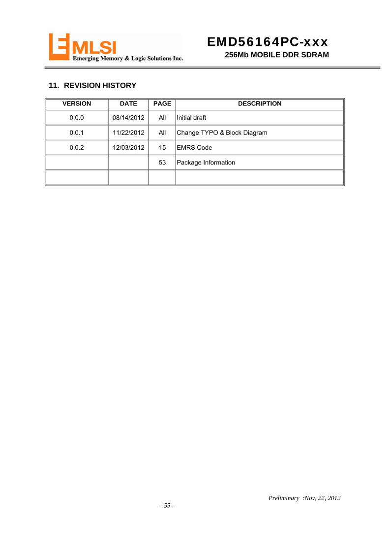
EMD56164PC-xxx 256Mb MOBILE DDR SDRAM
Preliminary :Nov, 22, 2012 - 55 -
11. REVISION HISTORY
VERSION DATE PAGE DESCRIPTION
0.0.0 08/14/2012 All Initial draft
0.0.1 11/22/2012 All Change TYPO & Block Diagram
0.0.2 12/03/2012 15 EMRS Code
53 Package Information
EMD56164PC-xxx 256Mb MOBILE DDR SDRAM
Preliminary :Nov, 22, 2012 - 56 -
Important Notice EMLSI products are not designed, intended, authorized or warranted for use as components in systems or equipment intended for surgical implantation, atomic energy control instruments, airplane or spaceship instruments, transportation instruments, traffic signal instruments, combustion control instruments, or for other applications intended to support or sustain life. Furthermore, EMLSI products are not intended for applications wherein failure of EMLSI products could result or lead to a situation where in personal injury, death or severe property or environmental damage could occur. EMLSI customers using or selling these products for use in such applications do so at their own risk and agree to fully indemnify EMLSI for any damages resulting from such improper use or sales.
------------------------------------------------------------------------------------------------------------------------------------------------- Please note that all data and specifications are subject to change without notice. All the trademarks of products and companies mentioned in the datasheet belong to their respective owners.


![User’s Manual (SMDK S5PV210 Rev0.0) - armedu.cnarmedu.cn/download/SMDKV210_Users_Manual_Rev0[1].0.pdf · User’s Manual (SMDK S5PV210 Rev0.0) Development Kit for S5PV210 Dec 02,](https://img.pdfslide.us/doc/110x75/5aad7caa7f8b9a8d678e3c4f/users-manual-smdk-s5pv210-rev00-10pdfusers-manual-smdk-s5pv210-rev00.jpg)
![M rTrNfi-]Nf~TrfC! G - p)]LAN'·, renvironmentclearance.nic.in/writereaddata/District/...MllilrTrNfi-]Nf~TrfC! p)]LAN'·, r jll_l ~G -r='_! y ~ INCLUDING PROGRESSIVE MINE CLOSURE PLAN](https://img.pdfslide.us/doc/110x75/60b729a220a87a2cf45b0dec/m-rtrnfi-nftrfc-g-plan-r-mllilrtrnfi-nftrfc-plan-r-jlll-g.jpg)