Embed Size (px)
Citation preview
Electronic Pack….. Chapter 6: Printed Circuit Board Design Slide 1
Chapter 6: Printed Circuit Board Design
Example of a Printed Circuit Board – front and back side
The course material was developed in INSIGTH II, a project sponsored by the Leonardo da Vinci program of the European Union
Electronic Pack….. Chapter 6: Printed Circuit Board Design Slide 2
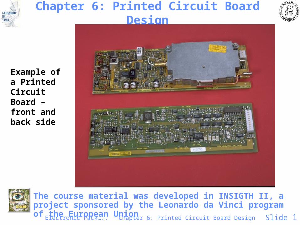
PCB Design, Introduction
• For new electronic products, designers are key persons, but should work in intimate cooperation with:
– Sales, marketing and customers
– Subcontractors– Production process experts– Cost engineers– Logistics and purchasing staff– etc.
Electronic Pack….. Chapter 6: Printed Circuit Board Design Slide 3
PCB Design, continued
• Advanced PCB CAD tools a neccessity–Schematics–Component Library–Critical Parameters (Placement Constraints, Electromagnetic Compatibility, Thermal Limitations, etc)
–Automatic Routing–Final Touch Manual Routing–(Verification by Final Simulation and Back Annotation)
Electronic Pack….. Chapter 6: Printed Circuit Board Design Slide 4
PCB CAD tools, continued
• Output:–Final Schematics–Assembly Drawings–Documentation for PWB Manufacturer (”Gerber” file giving input for making PWB Manucturing Data (See Chapter 5):
• Data for Photo- or Laser Plotter for Making Photographic Films and Printing Masks
• Data for Numeric Drilling and Milling Machines• Data for Placement Machines• Data for Test Fixtures and Testing Machines
Electronic Pack….. Chapter 6: Printed Circuit Board Design Slide 5
PCB Design, continued
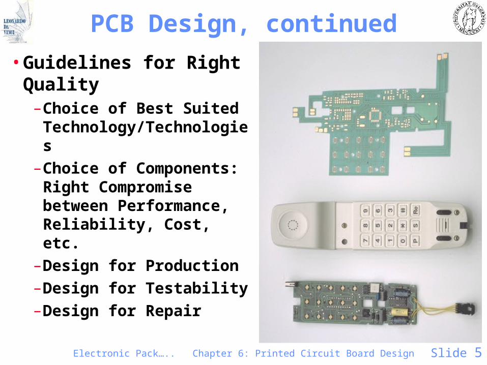
• Guidelines for Right Quality
–Choice of Best Suited Technology/Technologies
–Choice of Components: Right Compromise between Performance, Reliability, Cost, etc.
–Design for Production–Design for Testability–Design for Repair
Electronic Pack….. Chapter 6: Printed Circuit Board Design Slide 6
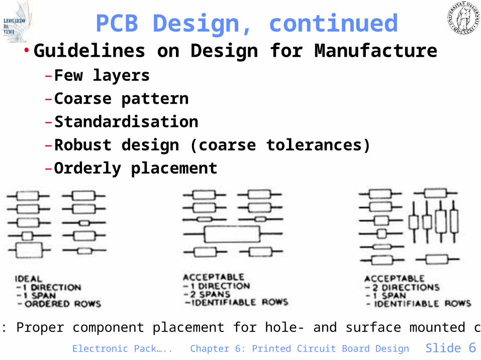
PCB Design, continued• Guidelines on Design for Manufacture
–Few layers–Coarse pattern–Standardisation–Robust design (coarse tolerances)–Orderly placement
Fig. 6.1.a: Proper component placement for hole- and surface mounted components
Electronic Pack….. Chapter 6: Printed Circuit Board Design Slide 7
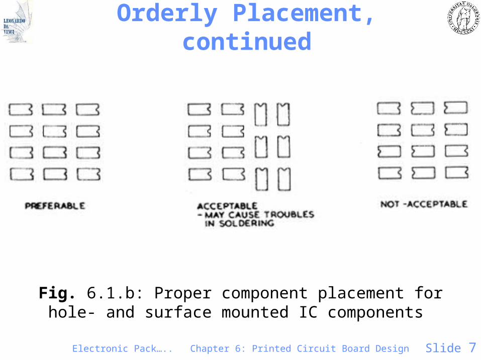
Orderly Placement, continued
Fig. 6.1.b: Proper component placement for hole- and surface mounted IC components
Electronic Pack….. Chapter 6: Printed Circuit Board Design Slide 8
PCB Design, continued
• Important Guideline for "Robust Design": – Circuits should function with large parameter
tolerances:• Design windows allowing for variations in
component parameters.• Process windows allowing for variations in each
process step.
– Regulatory requirements on safety and EMC should be passed within the specified design and process windows.
Electronic Pack….. Chapter 6: Printed Circuit Board Design Slide 9
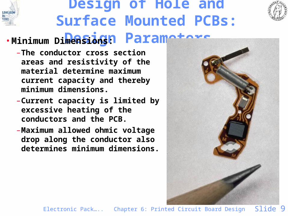
Design of Hole and Surface Mounted PCBs: Design Parameters
• Minimum Dimensions:–The conductor cross section areas
and resistivity of the material determine maximum current capacity and thereby minimum dimensions.
–Current capacity is limited by excessive heating of the conductors and the PCB.
–Maximum allowed ohmic voltage drop along the conductor also determines minimum dimensions.
Electronic Pack….. Chapter 6: Printed Circuit Board Design Slide 10
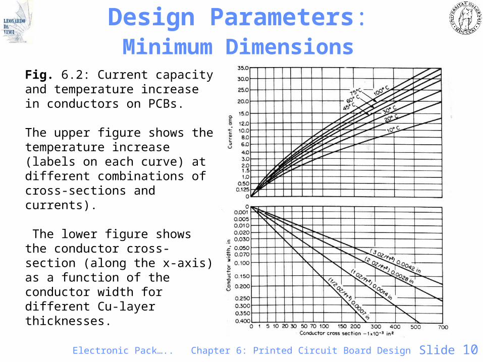
Design Parameters: Minimum Dimensions
Fig. 6.2: Current capacity and temperature increase in conductors on PCBs.
The upper figure shows the temperature increase (labels on each curve) at different combinations of cross-sections and currents).
The lower figure shows the conductor cross-section (along the x-axis) as a function of the conductor width for different Cu-layer thicknesses.
Electronic Pack….. Chapter 6: Printed Circuit Board Design Slide 11
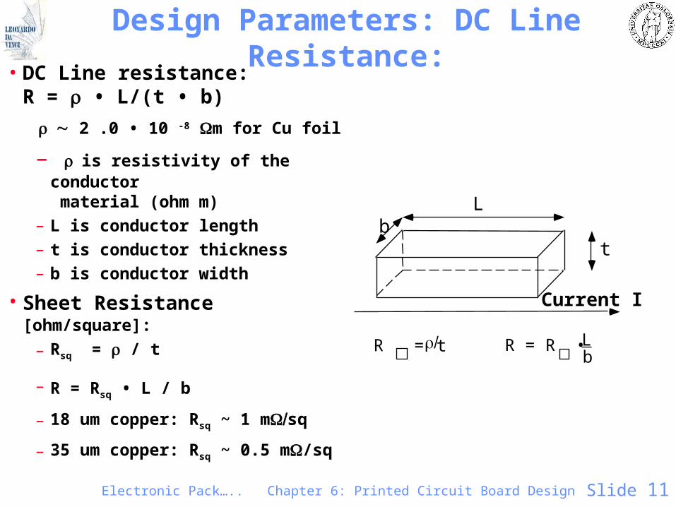
Design Parameters: DC Line Resistance:
• DC Line resistance:R = • L/(t • b)
2 .0 • 10 -8 m for Cu foil
– is resistivity of the conductor material (ohm m)
– L is conductor length
– t is conductor thickness
– b is conductor width
• Sheet Resistance [ohm/square]:
– Rsq = / t
– R = Rsq • L / b – 18 um copper: Rsq ~ 1 msq
– 35 um copper: Rsq ~ 0.5 m/sq
Lb
t
Current I
R = R •Lb
R = t
Electronic Pack….. Chapter 6: Printed Circuit Board Design Slide 12
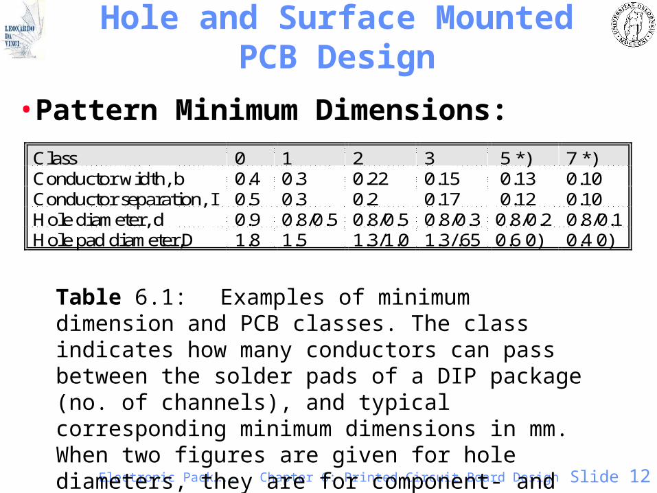
Hole and Surface Mounted PCB Design
• Pattern Minimum Dimensions:
Class 0 1 2 3 5 *) 7 *)Conductor width, b 0.4 0.3 0.22 0.15 0.13 0.10Conductor separation, I 0.5 0.3 0.2 0.17 0.12 0.10Hole diameter, d 0.9 0.8/0.5 0.8/0.5 0.8/0.3 0.8/0.2 0.8/0.1Hole pad diameter,D 1.8 1.5 1.3/1.0 1.3/.65 0.6 0) 0.4 0)
Table 6.1: Examples of minimum dimension and PCB classes. The class indicates how many conductors can pass between the solder pads of a DIP package (no. of channels), and typical corresponding minimum dimensions in mm. When two figures are given for hole diameters, they are for component- and via holes respectively.
Electronic Pack….. Chapter 6: Printed Circuit Board Design Slide 13
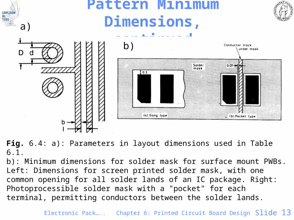
Pattern Minimum Dimensions,continued
Fig. 6.4: a): Parameters in layout dimensions used in Table 6.1. b): Minimum dimensions for solder mask for surface mount PWBs. Left: Dimensions for screen printed solder mask, with one common opening for all solder lands of an IC package. Right: Photoprocessible solder mask with a "pocket" for each terminal, permitting conductors between the solder lands.
b)
a)
Electronic Pack….. Chapter 6: Printed Circuit Board Design Slide 14
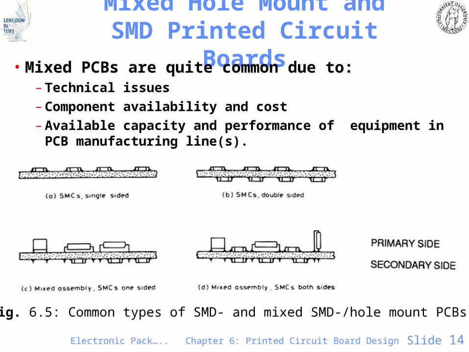
Mixed Hole Mount and SMD Printed Circuit Boards
• Mixed PCBs are quite common due to:– Technical issues– Component availability and cost– Available capacity and performance of equipment in PCB
manufacturing line(s).
Fig. 6.5: Common types of SMD- and mixed SMD-/hole mount PCBs.
Electronic Pack….. Chapter 6: Printed Circuit Board Design Slide 15
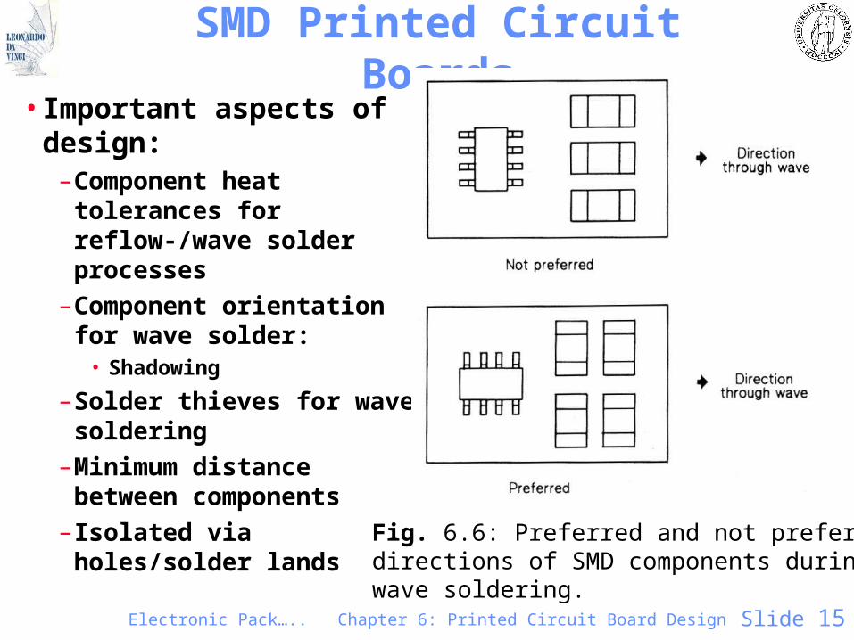
SMD Printed Circuit Boards• Important aspects of
design:–Component heat
tolerances for reflow-/wave solder processes
–Component orientation for wave solder:
• Shadowing
–Solder thieves for wave soldering
–Minimum distance between components
– Isolated via holes/solder lands
Fig. 6.6: Preferred and not preferred directions of SMD components during wave soldering.
Electronic Pack….. Chapter 6: Printed Circuit Board Design Slide 16
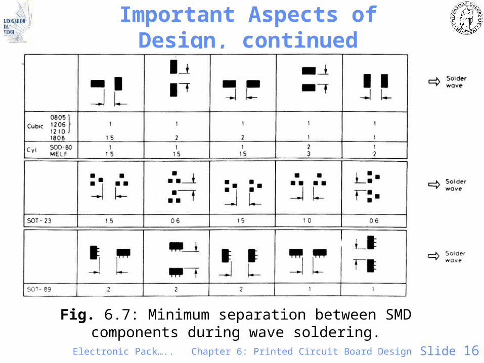
Important Aspects of Design, continued
Fig. 6.7: Minimum separation between SMD components during wave soldering.
Electronic Pack….. Chapter 6: Printed Circuit Board Design Slide 17
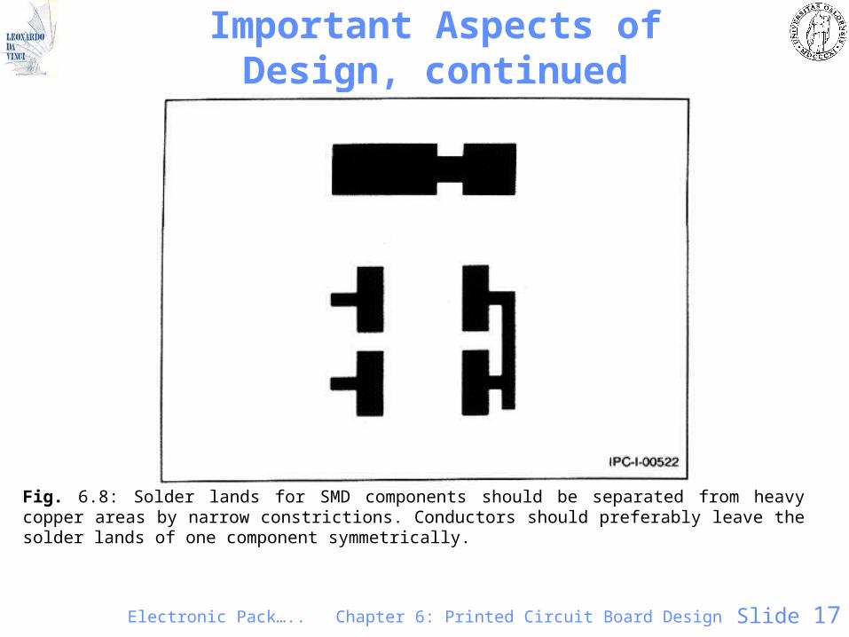
Important Aspects of Design, continued
Fig. 6.8: Solder lands for SMD components should be separated from heavy copper areas by narrow constrictions. Conductors should preferably leave the solder lands of one component symmetrically.
Electronic Pack….. Chapter 6: Printed Circuit Board Design Slide 18
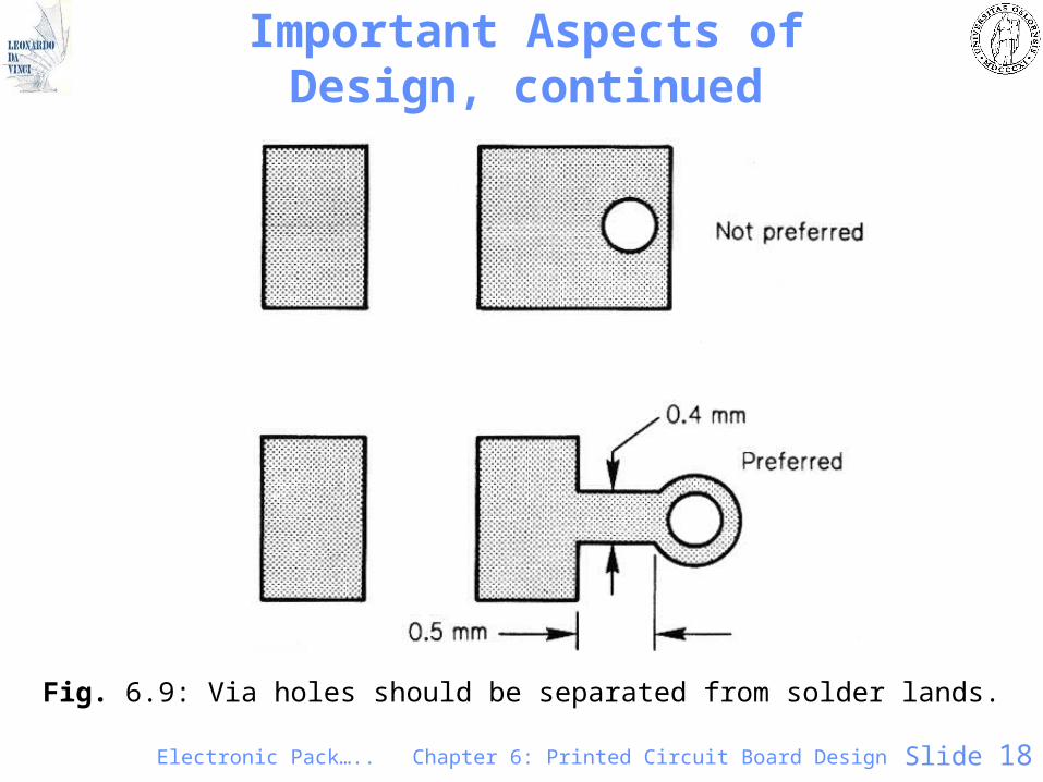
Important Aspects of Design, continued
Fig. 6.9: Via holes should be separated from solder lands.
Electronic Pack….. Chapter 6: Printed Circuit Board Design Slide 19
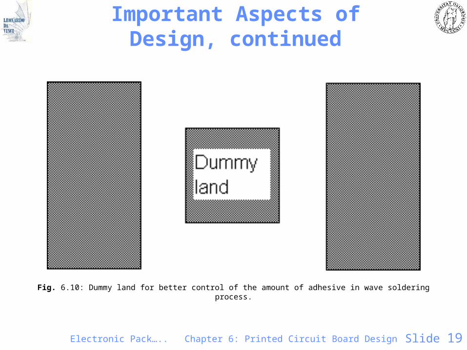
Important Aspects of Design, continued
Fig. 6.10: Dummy land for better control of the amount of adhesive in wave soldering process.
Electronic Pack….. Chapter 6: Printed Circuit Board Design Slide 20
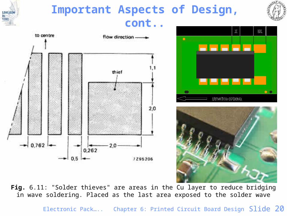
Important Aspects of Design, cont..
Fig. 6.11: "Solder thieves" are areas in the Cu layer to reduce bridging in wave soldering. Placed as the last area exposed to the solder wave
Electronic Pack….. Chapter 6: Printed Circuit Board Design Slide 21
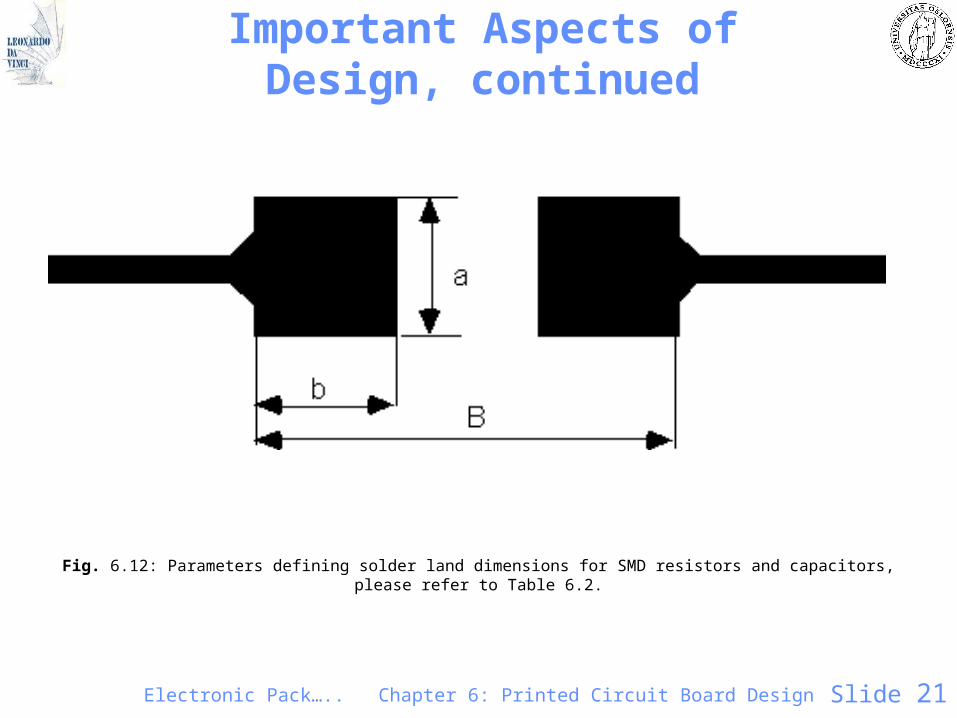
Important Aspects of Design, continued
Fig. 6.12: Parameters defining solder land dimensions for SMD resistors and capacitors, please refer to Table 6.2.
Electronic Pack….. Chapter 6: Printed Circuit Board Design Slide 22
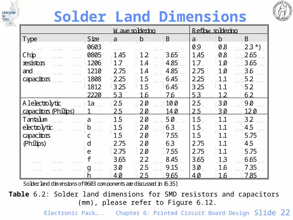
Solder Land Dimensions
Table 6.2: Solder land dimensions for SMD resistors and capacitors (mm), please refer to Figure 6.12.
Wave soldering Reflow solderingType Size a b B a b B
0603 0.9 0.8 2.3 *)Chip 0805 1.45 1.2 3.65 1.45 0.8 2.65resistors 1206 1.7 1.4 4.85 1.7 1.0 3.65and 1210 2.75 1.4 4.85 2.75 1.0 3.6capacitors 1808 2.25 1.5 6.45 2.25 1.1 5.2
1812 3.25 1.5 6.45 3.25 1.1 5.22220 5.3 1.6 7.6 5.3 1.2 6.2
Al electrolytic 1a 2.5 2.0 10.0 2.5 3.0 9.0capacitors (Philips) 1 2.5 2.0 14.0 2.5 3.0 12.0Tantalum a 1.5 2.0 5.0 1.5 1.1 3.2electrolytic b 1.5 2.0 6.3 1.5 1.1 4.5capacitors c 1.5 2.0 7.55 1.5 1.1 5.75(Philips) d 2.75 2.0 6.3 2.75 1.1 4.5
e 2.75 2.0 7.55 2.75 1.1 5.75f 3.65 2.2 8.45 3.65 1.3 6.65g 3.0 2.5 9.15 3.0 1.6 7.35h 4.0 2.5 9.65 4.0 1.6 7.85
Solder land dimensions of 0603 components are discussed in [6.35]
Electronic Pack….. Chapter 6: Printed Circuit Board Design Slide 23
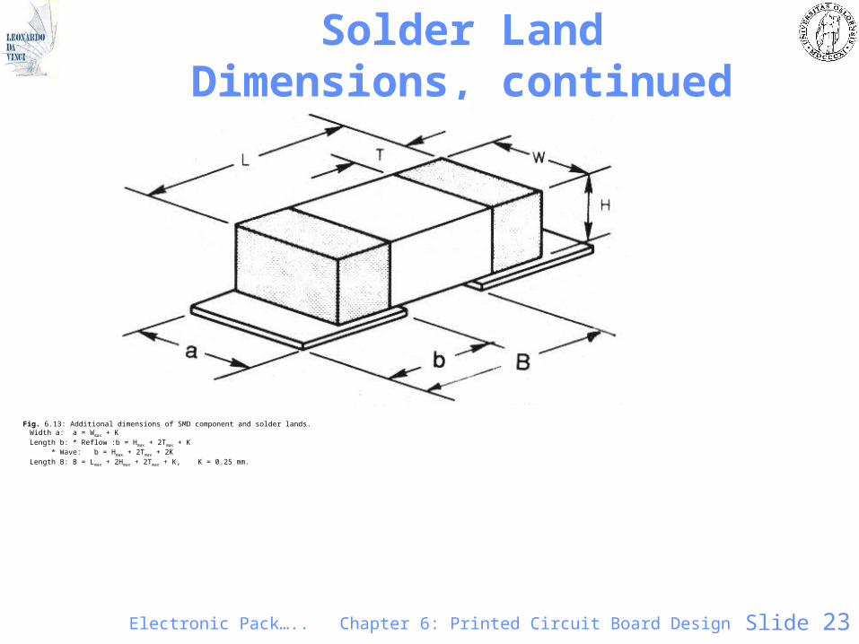
Solder Land Dimensions, continued
Fig. 6.13: Additional dimensions of SMD component and solder lands. Width a: a = Wmax + K Length b: * Reflow : b = Hmax + 2Tmax + K * Wave: b = Hmax + 2Tmax + 2K Length B: B = Lmax + 2Hmax + 2Tmax + K, K = 0.25 mm.
Electronic Pack….. Chapter 6: Printed Circuit Board Design Slide 24
Solder Land Dimensions, continued
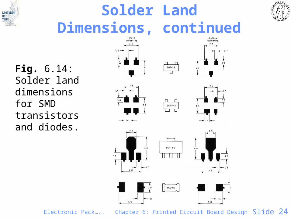
Fig. 6.14: Solder land dimensions for SMD transistors and diodes.
Electronic Pack….. Chapter 6: Printed Circuit Board Design Slide 25
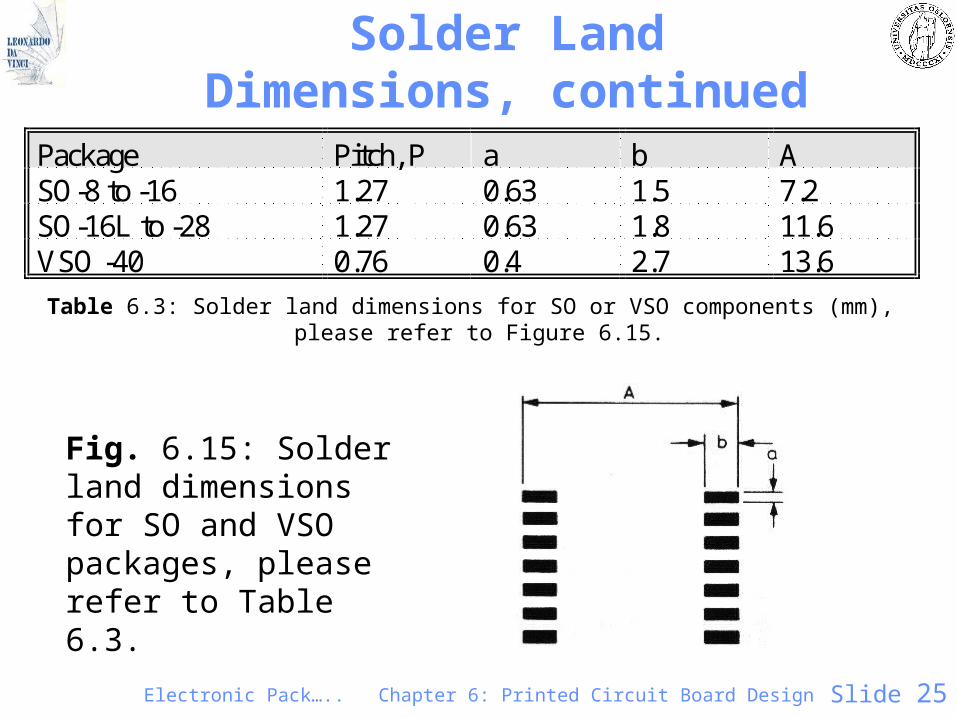
Solder Land Dimensions, continued
Table 6.3: Solder land dimensions for SO or VSO components (mm), please refer to Figure 6.15.
Package Pitch, P a b ASO-8 to -16 1.27 0.63 1.5 7.2SO-16L to -28 1.27 0.63 1.8 11.6VSO -40 0.76 0.4 2.7 13.6
Fig. 6.15: Solder land dimensions for SO and VSO packages, please refer to Table 6.3.
Electronic Pack….. Chapter 6: Printed Circuit Board Design Slide 26
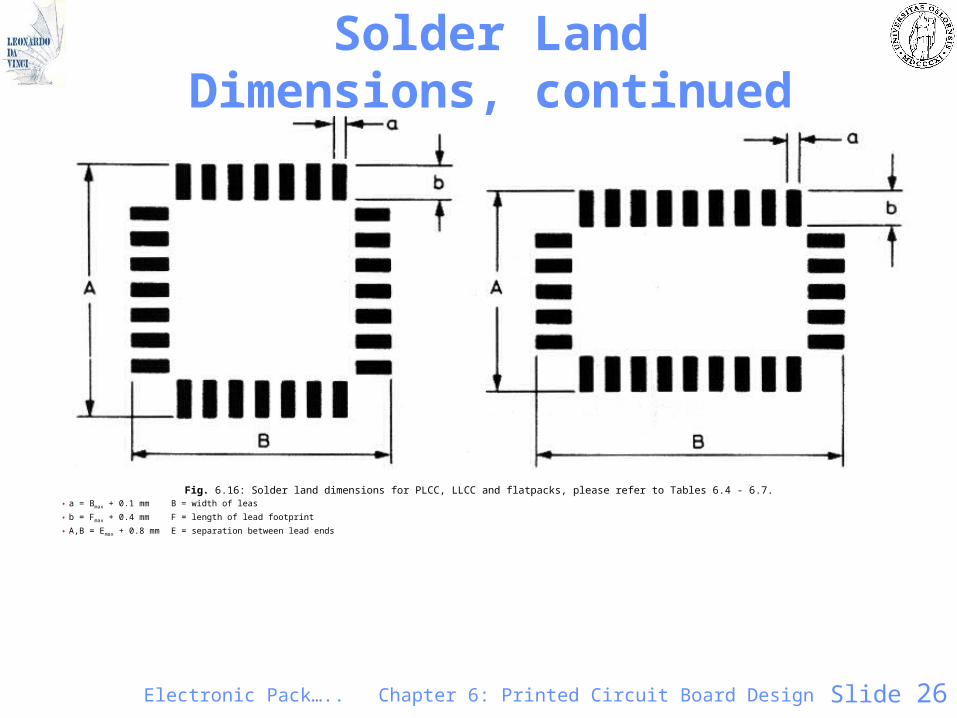
Solder Land Dimensions, continued
Fig. 6.16: Solder land dimensions for PLCC, LLCC and flatpacks, please refer to Tables 6.4 - 6.7.• a = Bmax + 0.1 mm B = width of leas
• b = Fmax + 0.4 mm F = length of lead footprint
• A,B = Emax + 0.8 mm E = separation between lead ends
Electronic Pack….. Chapter 6: Printed Circuit Board Design Slide 27
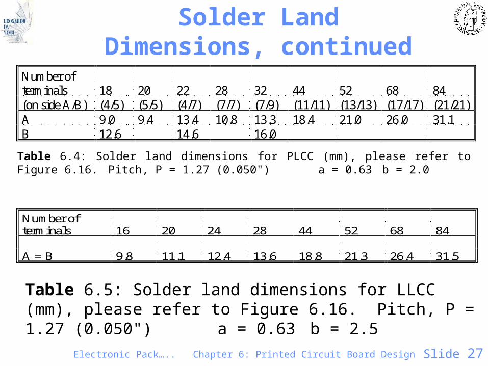
Solder Land Dimensions, continued
Table 6.4: Solder land dimensions for PLCC (mm), please refer to Figure 6.16. Pitch, P = 1.27 (0.050") a = 0.63 b = 2.0
Number ofterminals 18 20 22 28 32 44 52 68 84(on side A/B) (4/5) (5/5) (4/7) (7/7) (7/9) (11/11) (13/13) (17/17) (21/21)A 9.0 9.4 13.4 10.8 13.3 18.4 21.0 26.0 31.1B 12.6 14.6 16.0
Number ofterminals 16 20 24 28 44 52 68 84
A = B 9.8 11.1 12.4 13.6 18.8 21.3 26.4 31.5
Table 6.5: Solder land dimensions for LLCC (mm), please refer to Figure 6.16. Pitch, P = 1.27 (0.050") a = 0.63 b = 2.5
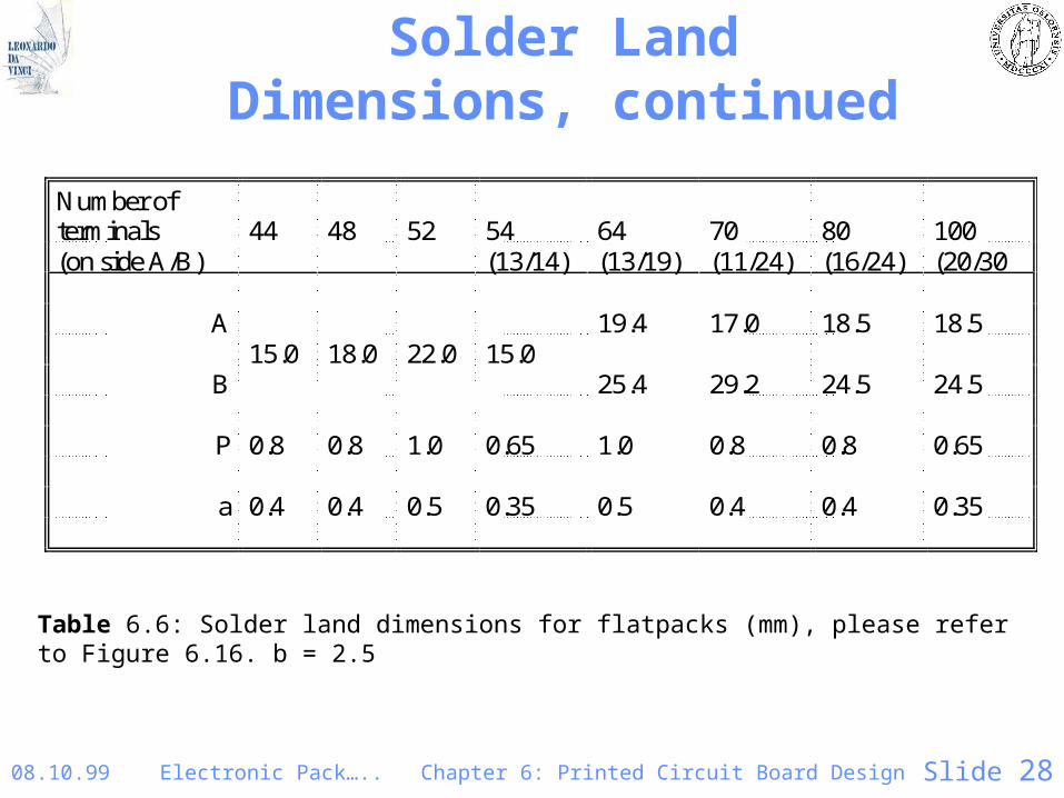
08.10.99 Electronic Pack….. Chapter 6: Printed Circuit Board Design Slide 28
Solder Land Dimensions, continued
Table 6.6: Solder land dimensions for flatpacks (mm), please refer to Figure 6.16. b = 2.5
Number ofterminals 44 48 52 54 64 70 80 100(on side A/B) (13/14) (13/19) (11/24) (16/24) (20/30
A 19.4 17.0 18.5 18.515.0 18.0 22.0 15.0
B 25.4 29.2 24.5 24.5
P 0.8 0.8 1.0 0.65 1.0 0.8 0.8 0.65
a 0.4 0.4 0.5 0.35 0.5 0.4 0.4 0.35
Electronic Pack….. Chapter 6: Printed Circuit Board Design Slide 29
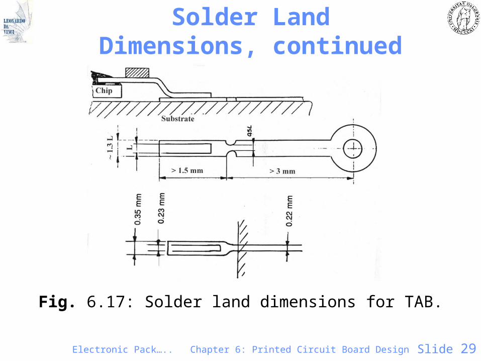
Solder Land Dimensions, continued
Fig. 6.17: Solder land dimensions for TAB.
Electronic Pack….. Chapter 6: Printed Circuit Board Design Slide 30
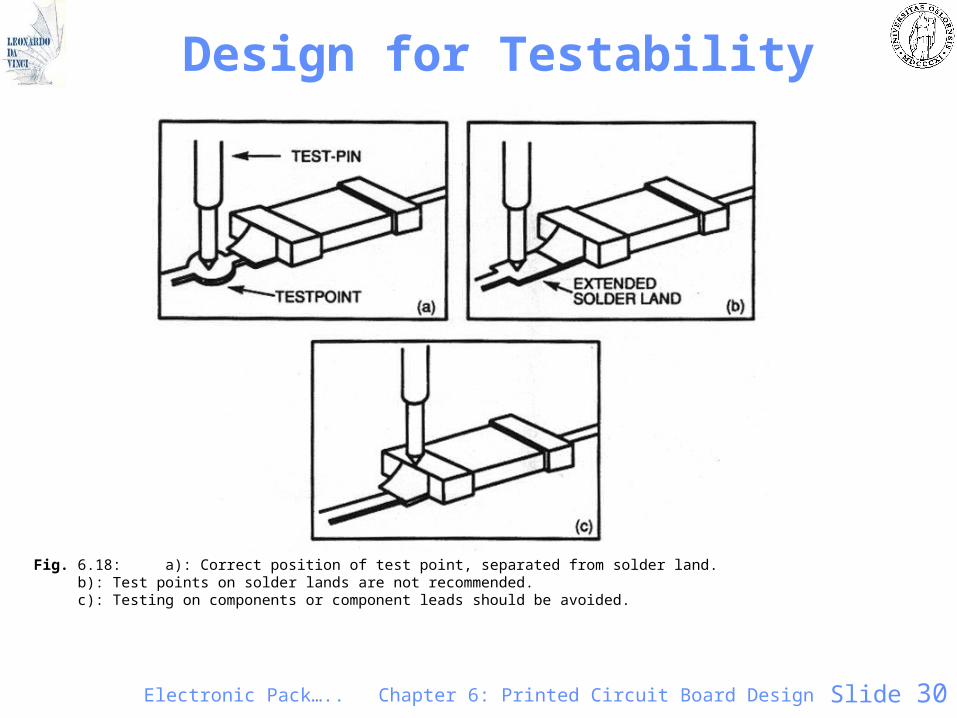
Design for Testability
Fig. 6.18: a): Correct position of test point, separated from solder land. b): Test points on solder lands are not recommended. c): Testing on components or component leads should be avoided.
Electronic Pack….. Chapter 6: Printed Circuit Board Design Slide 31
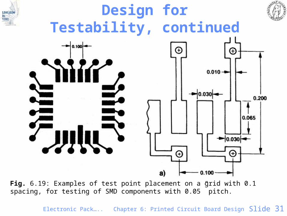
Design for Testability, continued
Fig. 6.19: Examples of test point placement on a grid with 0.1” spacing, for testing of SMD components with 0.05” pitch.

Electronic Pack….. Chapter 6: Printed Circuit Board Design Slide 32
Testability• Defect level:
• DL (ppm) = 1 - Y(1-T) x 106 • DL = defect level• Y = yield • T = fault coverage (One cannot test all failure modes)
• Test Methods– Functional test (Test the PCB in the system – PCB OK or not)– In-circuit test (Test at local test points – finds the exact fault)– Scan path (For logic circuits – digital output versus input)– Boundary scan (Scan path with separate test pins)– Built-in self test (Add test circuitry on the PCB)
Electronic Pack….. Chapter 6: Printed Circuit Board Design Slide 33
Test Principles• Guidelines for Test Strategy for In-circuit test
– Single sided (normally) - double sided test fixtures are expensive and less robust
– Separate test points - avoid using component leads or solder lands
– 0.1" grid (normally) - 0.05 ” test probes are fragile (0.1" is 2.5mm)
– Solder on test points for reliable contact– Watch out and consider possible problems with high
component– Modern equipment often uses flying probes:
Example on YouTube:http://www.youtube.com/watch?v=sj5yDyWw67w
Electronic Pack….. Chapter 6: Printed Circuit Board Design Slide 34
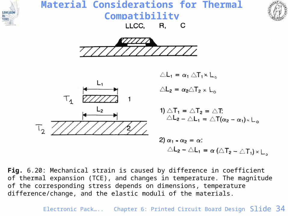
Material Considerations for Thermal Compatibility
Fig. 6.20: Mechanical strain is caused by difference in coefficient of thermal expansion (TCE), and changes in temperature. The magnitude of the corresponding stress depends on dimensions, temperature difference/change, and the elastic moduli of the materials.
Electronic Pack….. Chapter 6: Printed Circuit Board Design Slide 35
Thermal Design
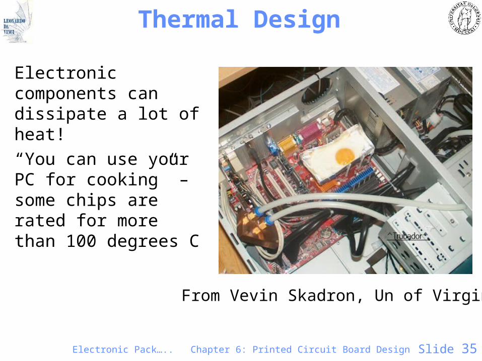
Electronic components can dissipate a lot of heat!
“You can use your PC for cooking” – some chips are rated for more than 100 degrees C
From Vevin Skadron, Un of Virginia
Electronic Pack….. Chapter 6: Printed Circuit Board Design Slide 36
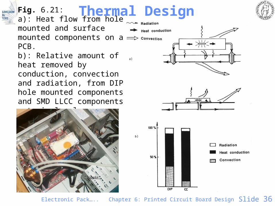
Thermal DesignFig. 6.21: a): Heat flow from hole mounted and surface mounted components on a PCB. b): Relative amount of heat removed by conduction, convection and radiation, from DIP hole mounted components and SMD LLCC components - typical values.
Electronic Pack….. Chapter 6: Printed Circuit Board Design Slide 37
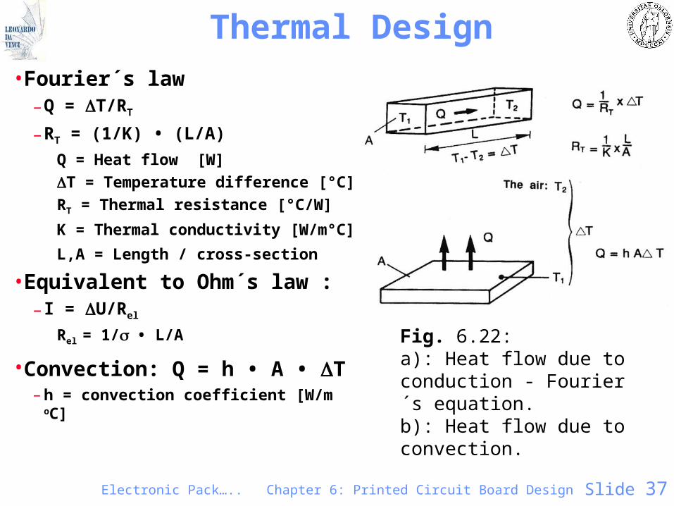
Thermal Design
•Fourier´s law–Q = T/RT
–RT = (1/K) • (L/A)
Q = Heat flow [W]
T = Temperature difference [°C]
RT = Thermal resistance [°C/W]
K = Thermal conductivity [W/m°C]
L,A = Length / cross-section
•Equivalent to Ohm´s law :– I = U/Rel
Rel = 1/• L/A
•Convection: Q = h • A • T – h = convection coefficient [W/m oC]
Fig. 6.22: a): Heat flow due to conduction - Fourier´s equation. b): Heat flow due to convection.
Electronic Pack….. Chapter 6: Printed Circuit Board Design Slide 38
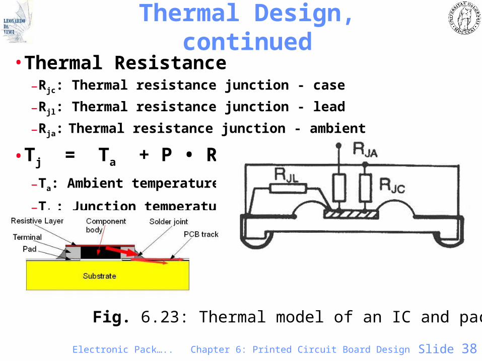
Thermal Design, continued•Thermal Resistance
–Rjc: Thermal resistance junction - case
–Rjl: Thermal resistance junction - lead
–Rja: Thermal resistance junction - ambient
•Tj = Ta + P • Rja
–Ta: Ambient temperature
–Tj : Junction temperature
Fig. 6.23: Thermal model of an IC and package.
Electronic Pack….. Chapter 6: Printed Circuit Board Design Slide 39
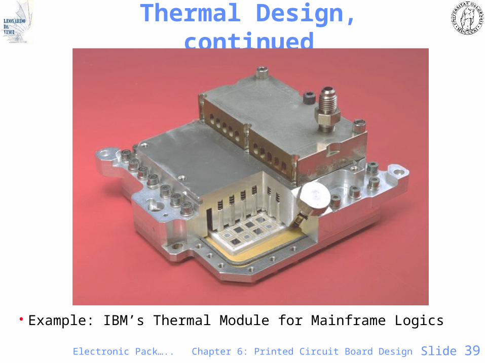
Thermal Design, continued
• Example: IBM’s Thermal Module for Mainframe Logics
Electronic Pack….. Chapter 6: Printed Circuit Board Design Slide 40
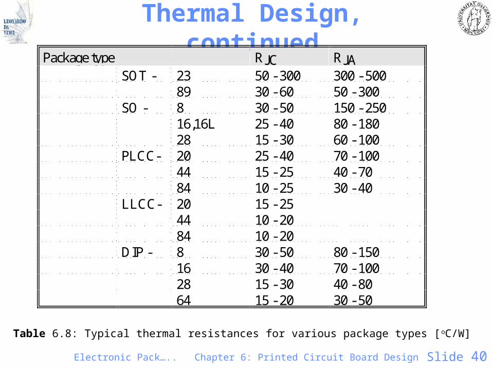
Thermal Design, continued
Table 6.8: Typical thermal resistances for various package types [oC/W]
Package type RJC RJASOT - 23 50 - 300 300 - 500
89 30 - 60 50 - 300SO - 8 30 - 50 150 - 250
16,16L 25 - 40 80 - 18028 15 - 30 60 - 100
PLCC- 20 25 - 40 70 - 10044 15 - 25 40 - 7084 10 - 25 30 - 40
LLCC- 20 15 - 2544 10 - 2084 10 - 20
DIP - 8 30 - 50 80 - 15016 30 - 40 70 - 10028 15 - 30 40 - 8064 15 - 20 30 - 50
Electronic Pack….. Chapter 6: Printed Circuit Board Design Slide 41
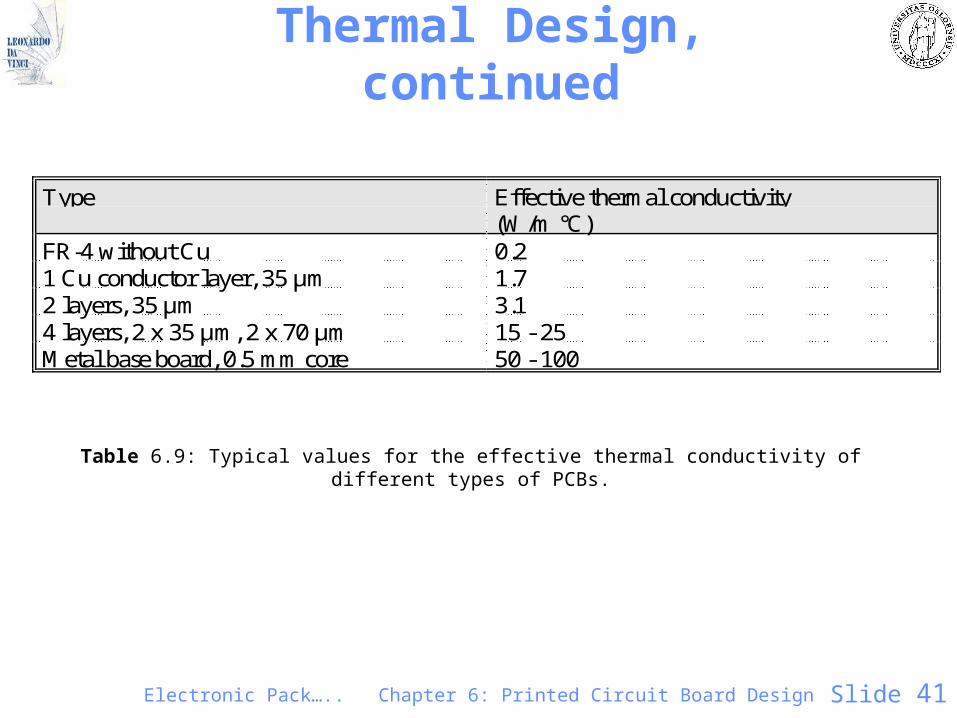
Thermal Design, continued
Table 6.9: Typical values for the effective thermal conductivity of different types of PCBs.
Type Effective thermal conductivity(W/m °C)
FR-4 without Cu 0.21 Cu conductor layer, 35 µm 1.72 layers, 35 µm 3.14 layers, 2 x 35 µm, 2 x 70 µm 15 - 25Metal base board, 0.5 mm core 50 - 100
Electronic Pack….. Chapter 6: Printed Circuit Board Design Slide 42
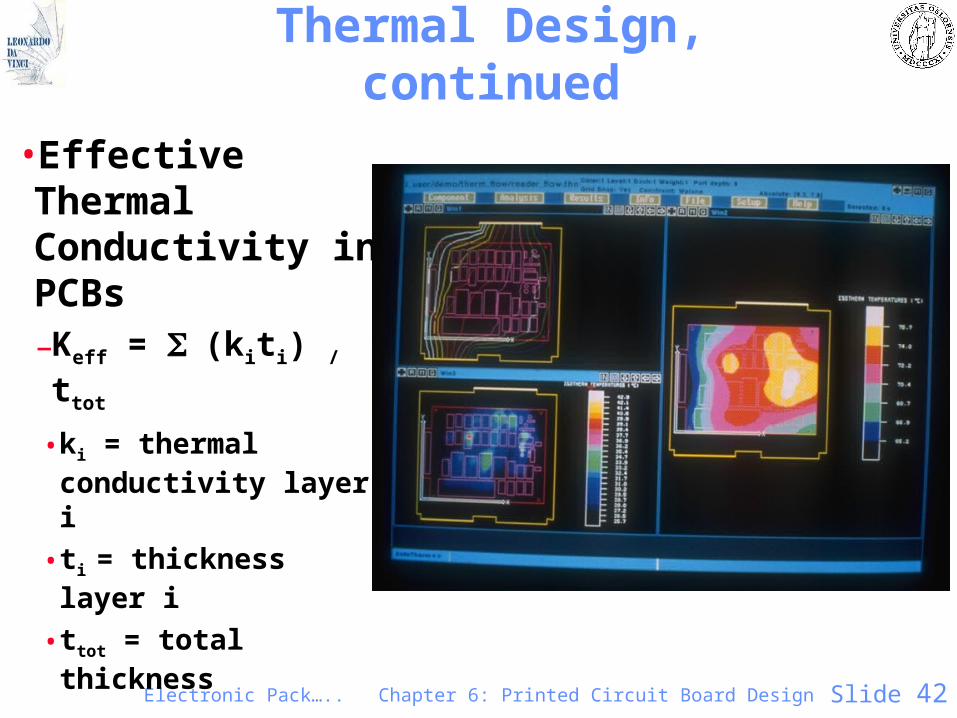
Thermal Design, continued
•Effective Thermal Conductivity in PCBs–Keff = (kiti) / ttot
• ki = thermal conductivity layer i
• ti = thickness layer i
• ttot = total thickness
Electronic Pack….. Chapter 6: Printed Circuit Board Design Slide 43
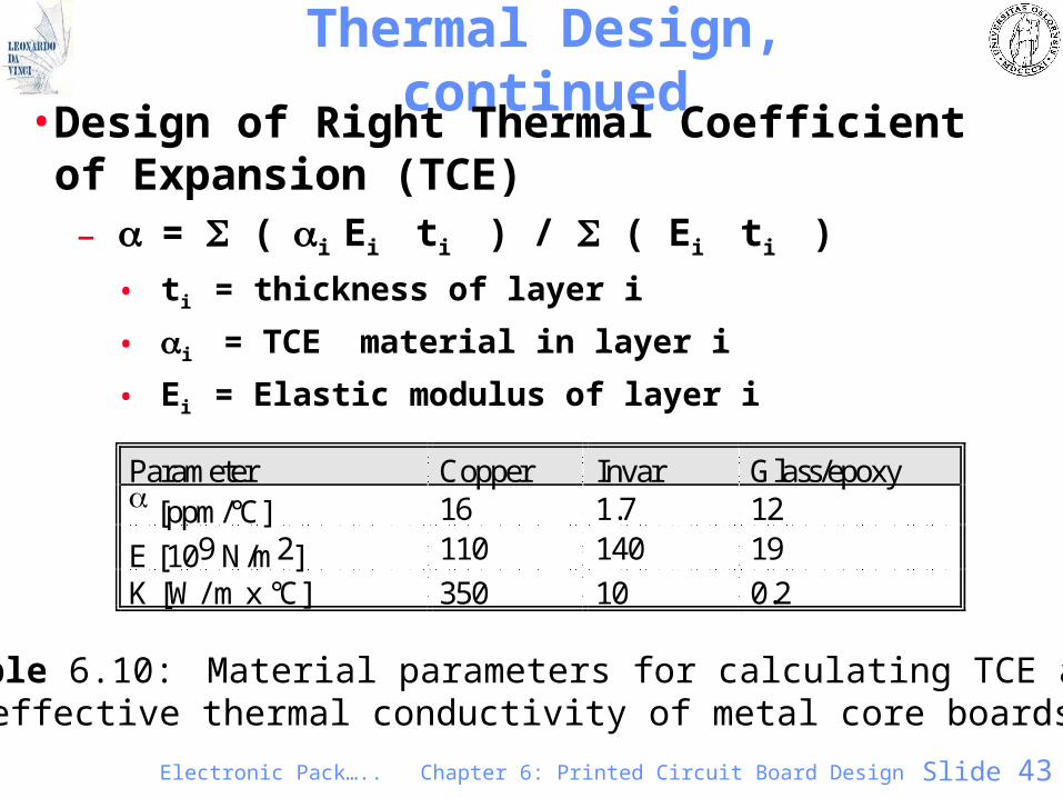
Thermal Design, continued• Design of Right Thermal Coefficient of
Expansion (TCE)– = (i Ei ti ) / ( Ei ti )
• ti = thickness of layer i
• i = TCE material in layer i
• Ei = Elastic modulus of layer i
Parameter Copper Invar Glass/epoxy [ppm/°C] 16 1.7 12
E [109 N/m2] 110 140 19
K [W/ m x °C] 350 10 0.2
Table 6.10: Material parameters for calculating TCE and effective thermal conductivity of metal core boards.
Electronic Pack….. Chapter 6: Printed Circuit Board Design Slide 44
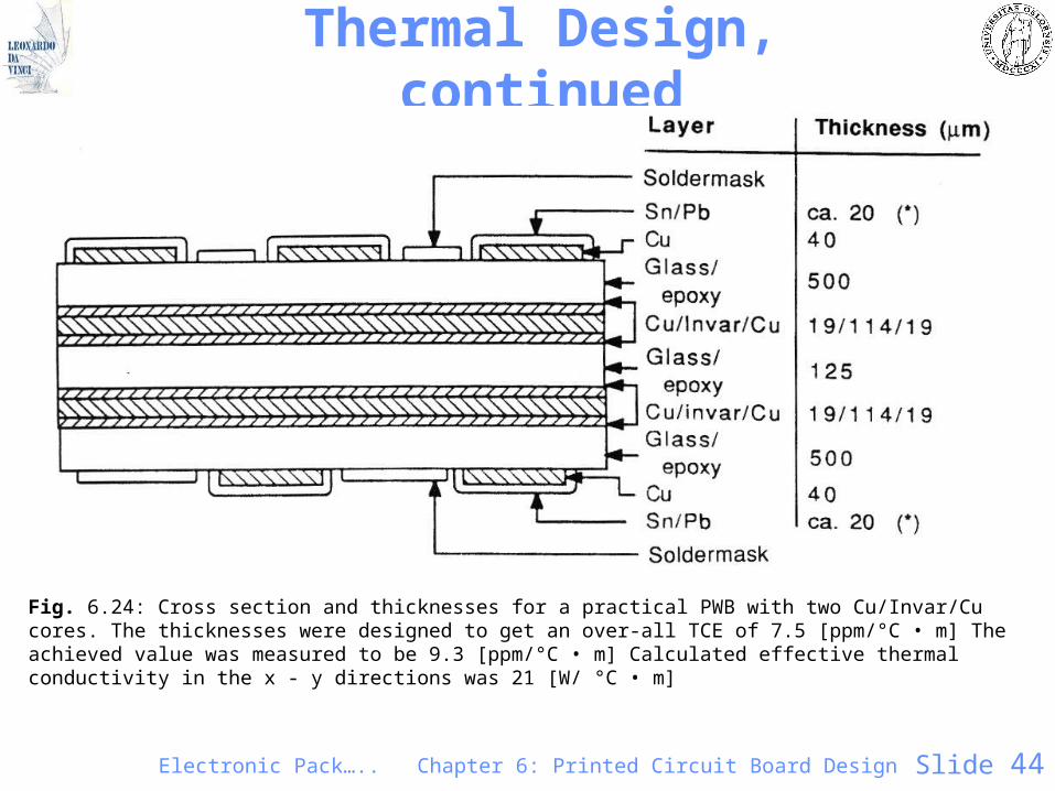
Thermal Design, continued
Fig. 6.24: Cross section and thicknesses for a practical PWB with two Cu/Invar/Cu cores. The thicknesses were designed to get an over-all TCE of 7.5 [ppm/°C • m] The achieved value was measured to be 9.3 [ppm/°C • m] Calculated effective thermal conductivity in the x - y directions was 21 [W/ °C • m]
Electronic Pack….. Chapter 6: Printed Circuit Board Design Slide 45
Thermal Design, continued
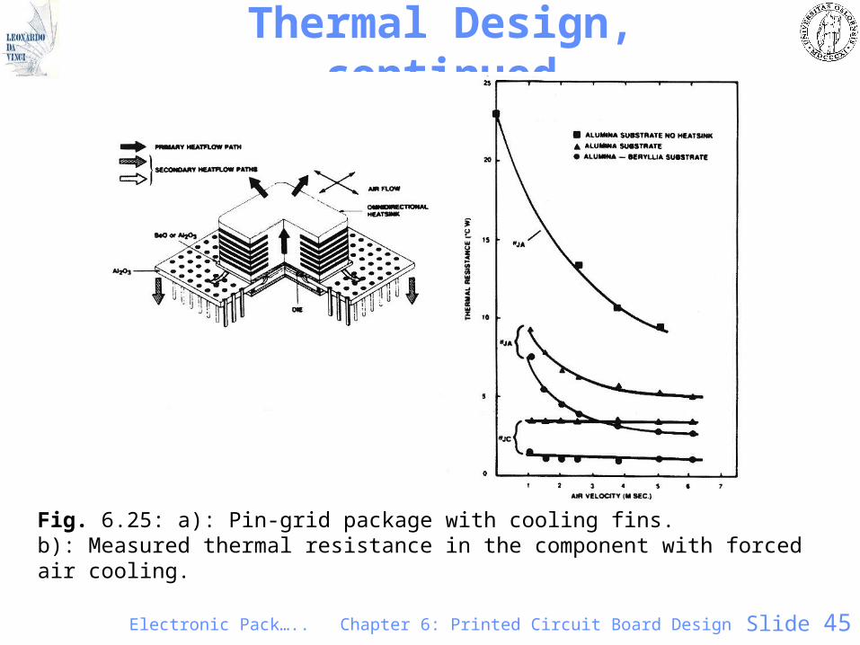
Fig. 6.25: a): Pin-grid package with cooling fins. b): Measured thermal resistance in the component with forced air cooling.
Electronic Pack….. Chapter 6: Printed Circuit Board Design Slide 46
Thermal Design, continued
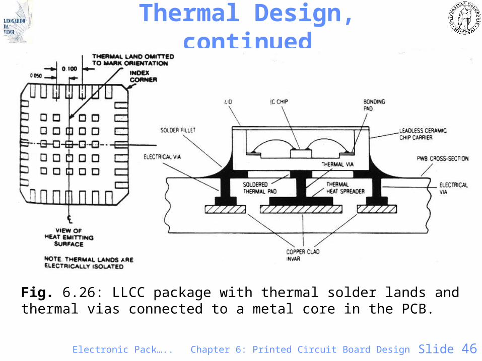
Fig. 6.26: LLCC package with thermal solder lands and thermal vias connected to a metal core in the PCB.
Electronic Pack….. Chapter 6: Printed Circuit Board Design Slide 47
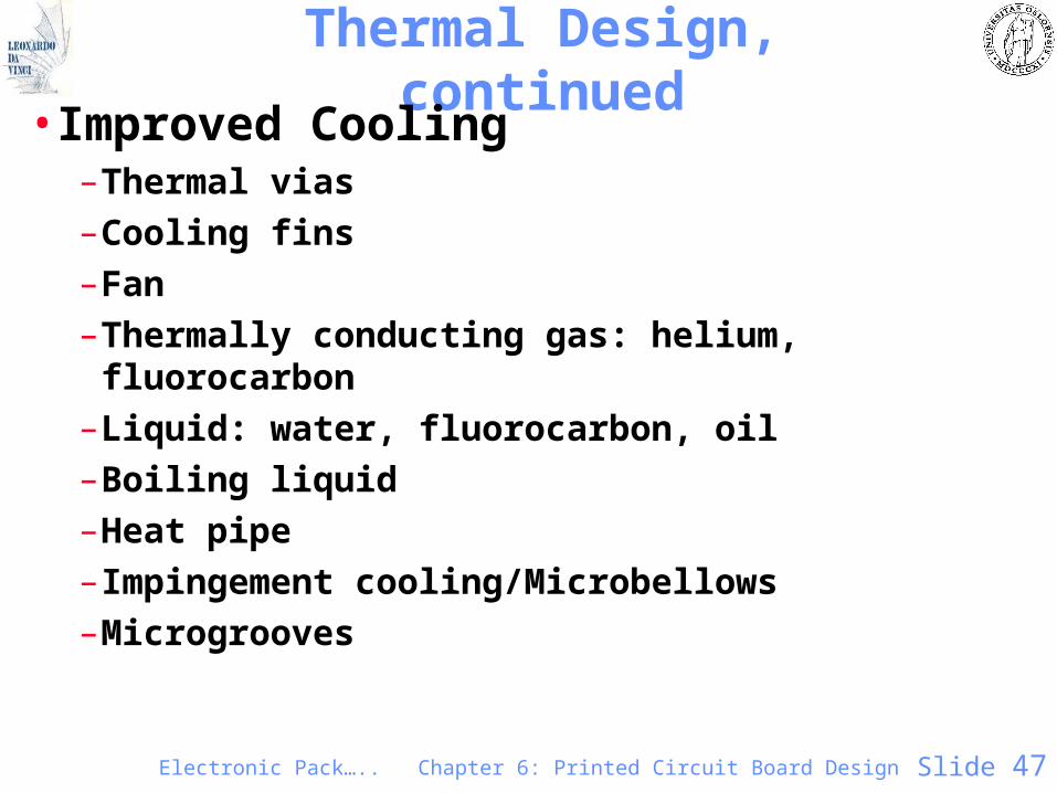
Thermal Design, continued• Improved Cooling
–Thermal vias–Cooling fins–Fan–Thermally conducting gas: helium, fluorocarbon–Liquid: water, fluorocarbon, oil–Boiling liquid–Heat pipe– Impingement cooling/Microbellows–Microgrooves
Electronic Pack….. Chapter 6: Printed Circuit Board Design Slide 48
Thermal Design, continued
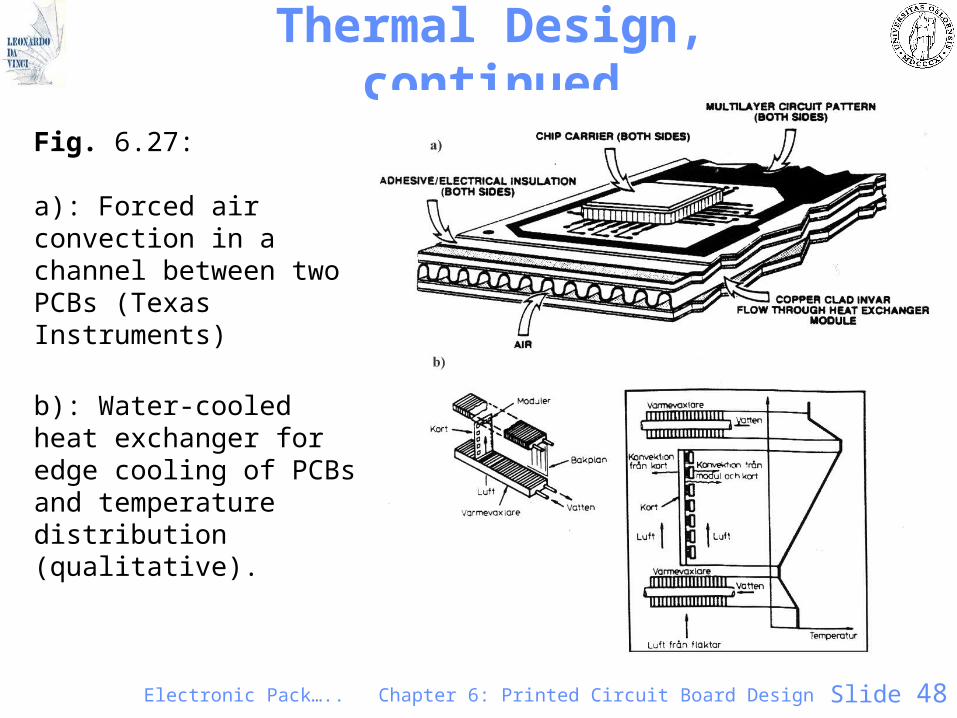
Fig. 6.27:
a): Forced air convection in a channel between two PCBs (Texas Instruments)
b): Water-cooled heat exchanger for edge cooling of PCBs and temperature distribution (qualitative).
Electronic Pack….. Chapter 6: Printed Circuit Board Design Slide 49
Thermal Design, continued
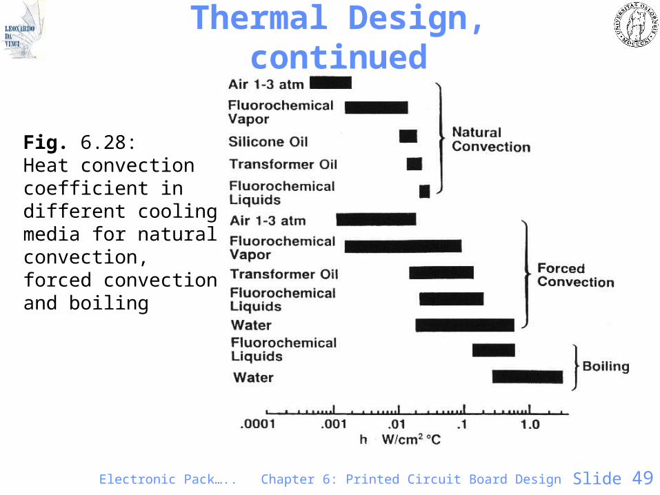
Fig. 6.28: Heat convection coefficient in different cooling media for natural convection, forced convection and boiling
Electronic Pack….. Chapter 6: Printed Circuit Board Design Slide 50
Thermal Design, continued
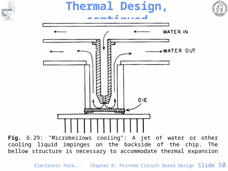
Fig. 6.29: "Microbellows cooling": A jet of water or other cooling liquid impinges on the backside of the chip. The bellow structure is necessary to accommodate thermal expansion
Electronic Pack….. Chapter 6: Printed Circuit Board Design Slide 51
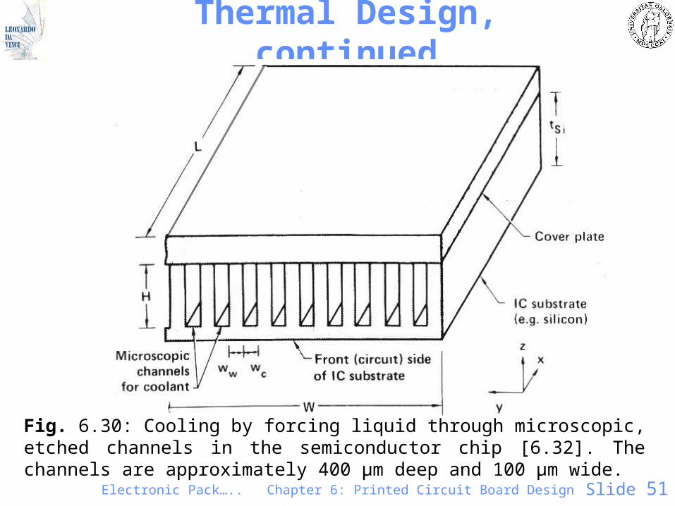
Thermal Design, continued
Fig. 6.30: Cooling by forcing liquid through microscopic, etched channels in the semiconductor chip [6.32]. The channels are approximately 400 µm deep and 100 µm wide.
Electronic Pack….. Chapter 6: Printed Circuit Board Design Slide 52
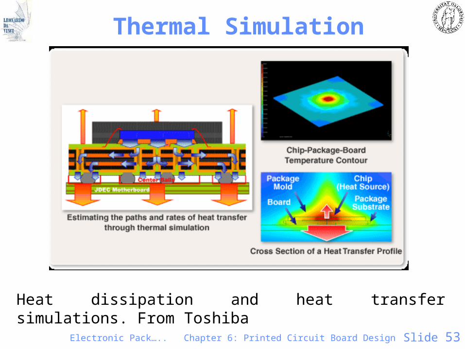
Thermal Simulation
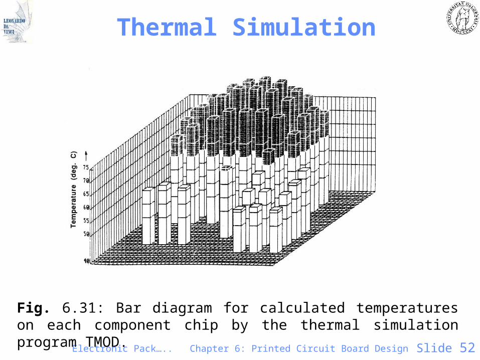
Fig. 6.31: Bar diagram for calculated temperatures on each component chip by the thermal simulation program TMOD.
Electronic Pack….. Chapter 6: Printed Circuit Board Design Slide 53
Thermal Simulation
Heat dissipation and heat transfer simulations. From Toshiba
Electronic Pack….. Chapter 6: Printed Circuit Board Design Slide 54
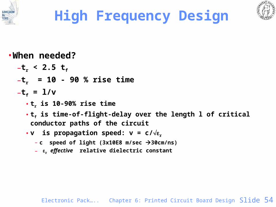
High Frequency Design
• When needed?–tr < 2.5 tf
–tr = 10 - 90 % rise time
–tf = l/v
• tr is 10-90% rise time
• tf is time-of-flight-delay over the length l of critical conductor paths of the circuit
• v is propagation speed: v = c/r
– c speed of light (3x10E8 m/sec 30cm/ns)
– r effective relative dielectric constant
55
56
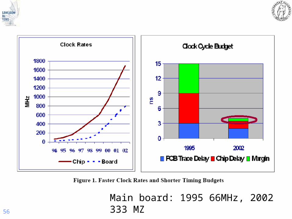
Main board: 1995 66MHz, 2002 333 MZ
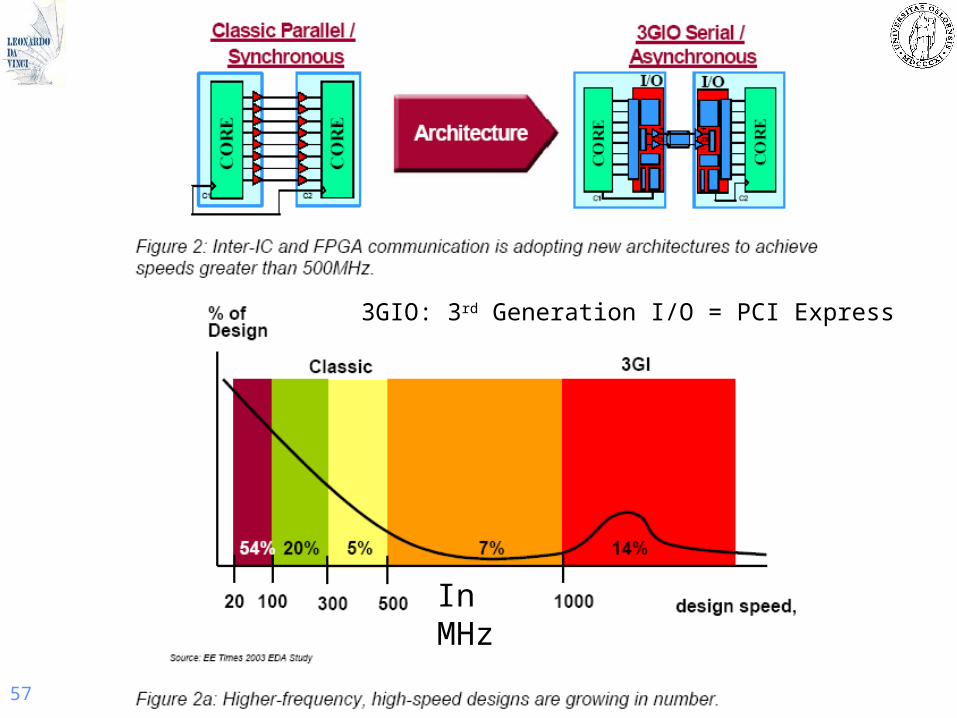
57
In MHz
3GIO: 3rd Generation I/O = PCI Express
Electronic Pack….. Chapter 6: Printed Circuit Board Design Slide 58
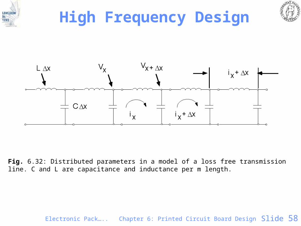
High Frequency Design
Fig. 6.32: Distributed parameters in a model of a loss free transmission line. C and L are capacitance and inductance per m length.
59
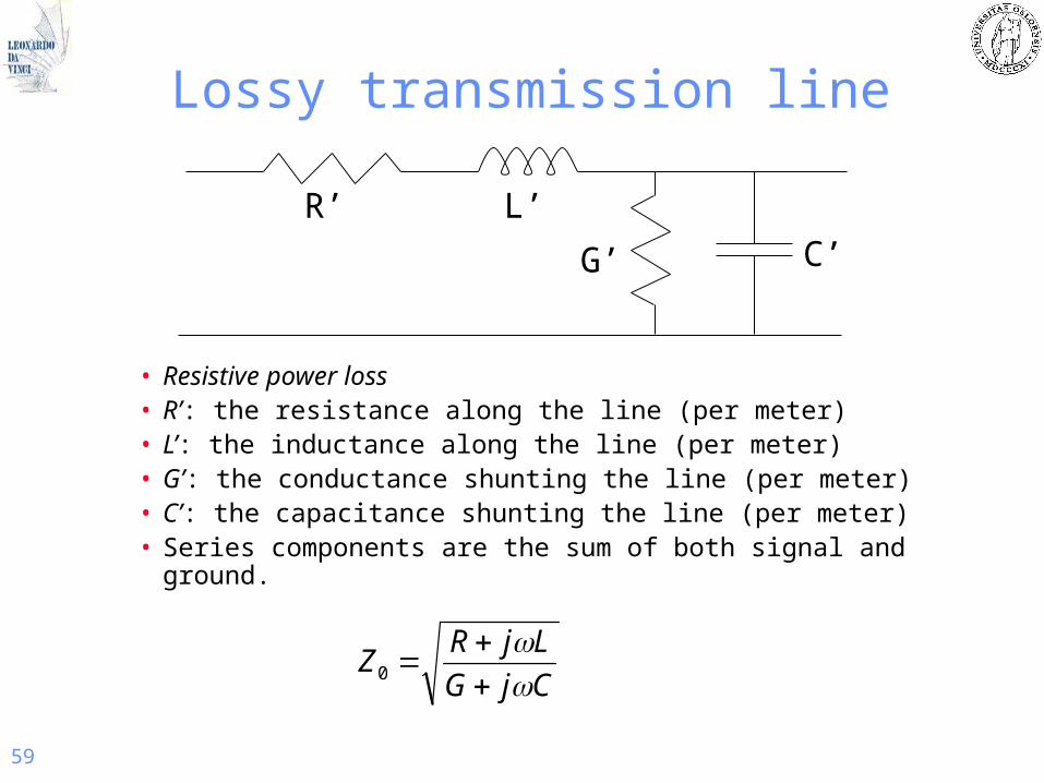
Lossy transmission line
• Resistive power loss• R’: the resistance along the line (per meter)• L’: the inductance along the line (per meter)• G’: the conductance shunting the line (per meter)• C’: the capacitance shunting the line (per meter)• Series components are the sum of both signal and ground.
R’ L’
G’ C’
CjG
LjRZ
0
Electronic Pack….. Chapter 6: Printed Circuit Board Design Slide 60
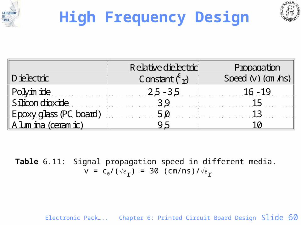
High Frequency Design
Table 6.11: Signal propagation speed in different media. v = c0/(r) = 30 (cm/ns)/r
DielectricRelative dielectric
Constant (r)Propagation
Speed (v) (cm/ns)
Polyimide 2,5 - 3,5 16 - 19Silicon dioxide 3,9 15Epoxy glass (PC board) 5,0 13Alumina (ceramic) 9,5 10
61
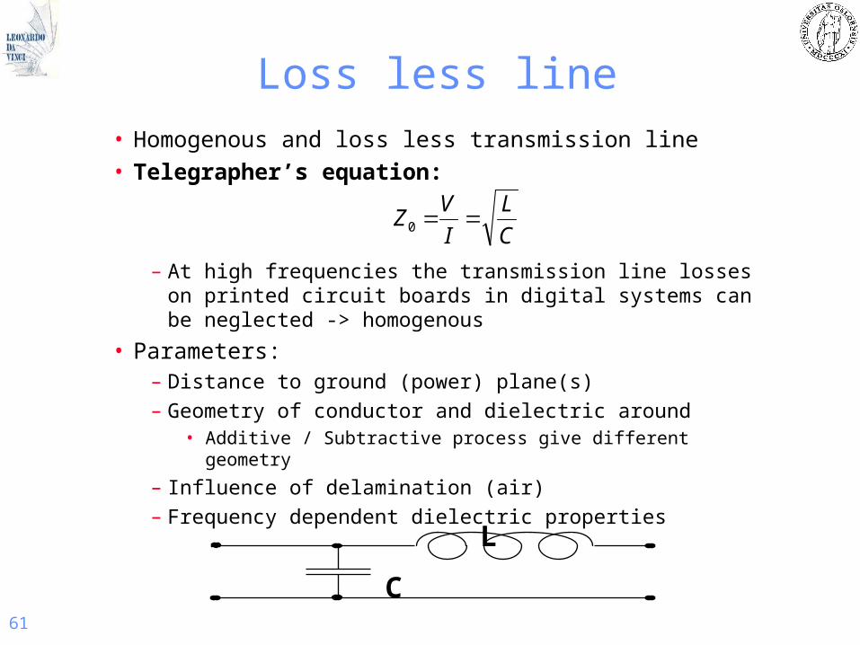
Loss less line• Homogenous and loss less transmission line
• Telegrapher’s equation:
– At high frequencies the transmission line losses on printed circuit boards in digital systems can be neglected -> homogenous
• Parameters:– Distance to ground (power) plane(s)
– Geometry of conductor and dielectric around• Additive / Subtractive process give different geometry
– Influence of delamination (air)
– Frequency dependent dielectric properties
C
L
C
L
I
VZ 0
Electronic Pack….. Chapter 6: Printed Circuit Board Design Slide 62
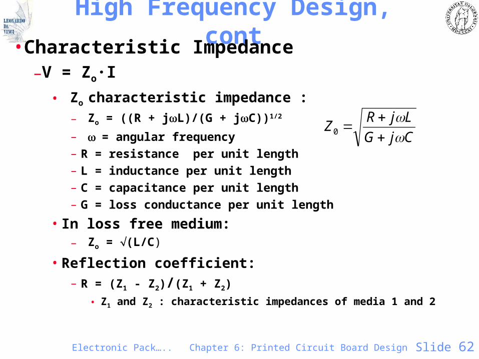
High Frequency Design, cont• Characteristic Impedance
–V = Zo·I
• Zo characteristic impedance :
– Zo = ((R + jL)/(G + jC))1/2
– = angular frequency– R = resistance per unit length– L = inductance per unit length– C = capacitance per unit length– G = loss conductance per unit length
• In loss free medium:– Zo = (L/C)
• Reflection coefficient:– R = (Z1 - Z2)/(Z1 + Z2)
• Z1 and Z2 : characteristic impedances of media 1 and 2
CjG
LjRZ
0
63
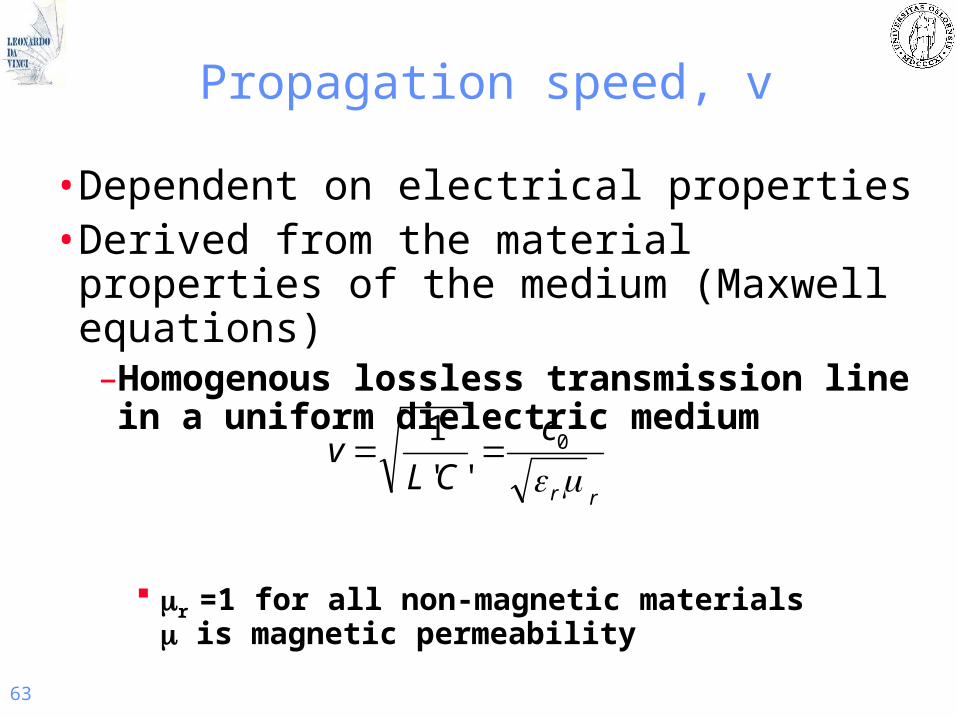
Propagation speed, v
• Dependent on electrical properties• Derived from the material properties of the
medium (Maxwell equations) –Homogenous lossless transmission line in a
uniform dielectric medium
r =1 for all non-magnetic materials is magnetic permeability
rr
c
CLv
0
''
1
64
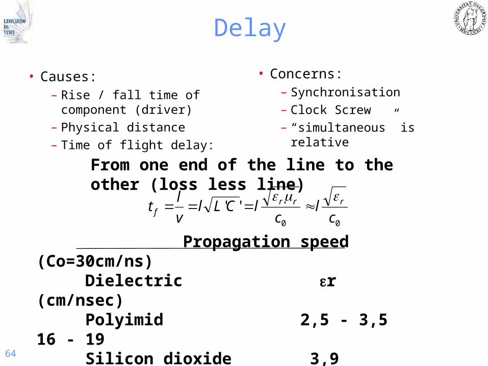
Delay
• Causes:– Rise / fall time of component
(driver)
– Physical distance
– Time of flight delay:
• Concerns:– Synchronisation
– Clock Screw
– “simultaneous” is relative
Propagation speed (Co=30cm/ns)Dielectric r (cm/nsec) Polyimid 2,5 - 3,5 16 - 19Silicon dioxide 3,9 15Epoxy glass (PCB) 4,2 - 5,0 13Alumina (ceramic) 9,5 10
00
''c
lc
lCLlv
lt rrr
f
From one end of the line to the other (loss less line)
65
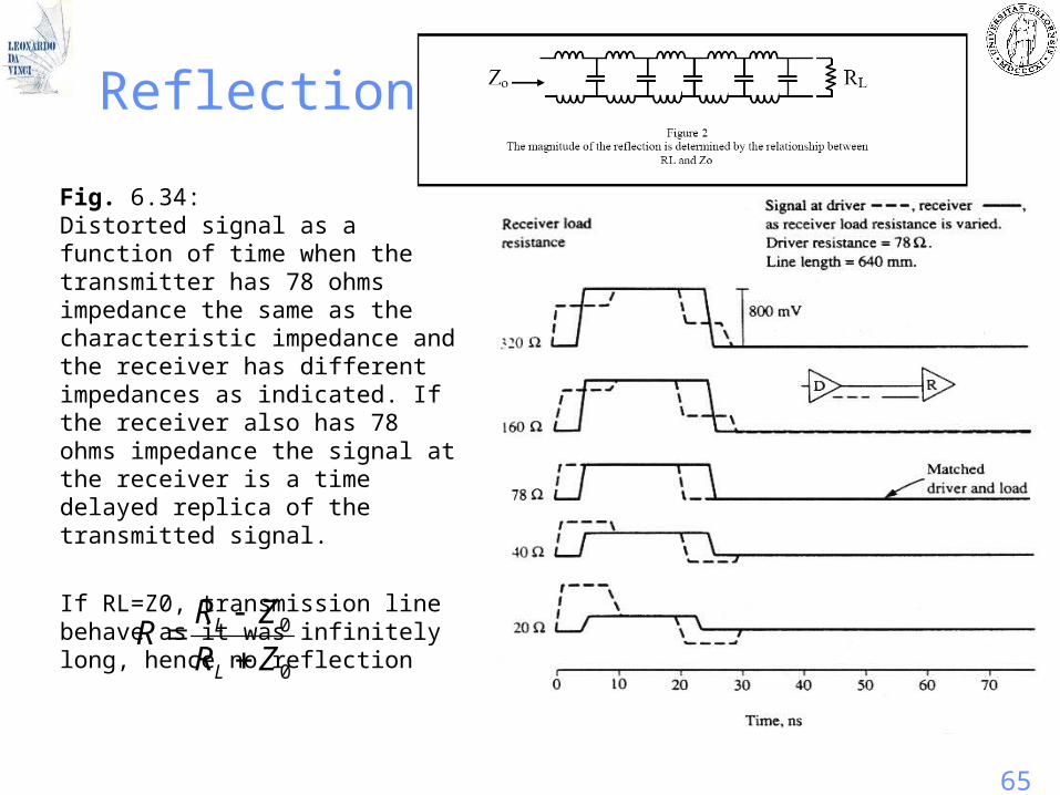
Reflections
Fig. 6.34:Distorted signal as a function of time when the transmitter has 78 ohms impedance the same as the characteristic impedance and the receiver has different impedances as indicated. If the receiver also has 78 ohms impedance the signal at the receiver is a time delayed replica of the transmitted signal.
If RL=Z0, transmission line behave as it was infinitely long, hence no reflection
0
0
ZR
ZRR
L
L
66
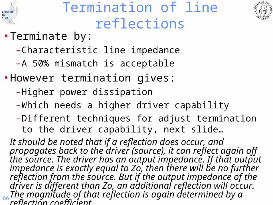
Termination of line reflections• Terminate by:
– Characteristic line impedance
– A 50% mismatch is acceptable
• However termination gives:– Higher power dissipation
– Which needs a higher driver capability
– Different techniques for adjust termination to the driver capability, next slide…
It should be noted that if a reflection does occur, and propagates back to the driver (source), it can reflect again off the source. The driver has an output impedance. If that output impedance is exactly equal to Zo, then there will be no further reflection from the source. But if the output impedance of the driver is different than Zo, an additional reflection will occur. The magnitude of that reflection is again determined by a reflection coefficient.
67
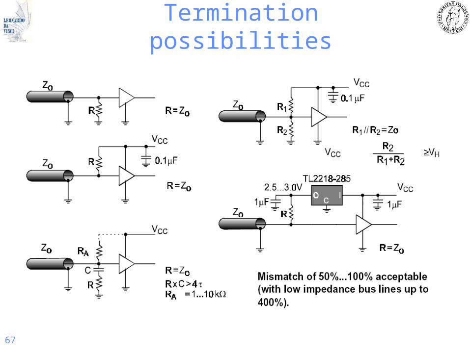
Termination possibilities
68
Reflections from other discontinuities
• In a typical PCB the characteristic impedance of the x and y wiring planes are not identical. (anisotrop media)
• Connection via forms a small inductive and capacitive discontinuity
• Other:– Connectors
– Corners and turns of the copper line• Do not use 90° turns
– Pins of IC packages
– Capacitors and terminating resistors
69
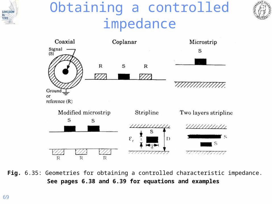
Obtaining a controlled impedance
Fig. 6.35: Geometries for obtaining a controlled characteristic impedance.
See pages 6.38 and 6.39 for equations and examples
Electronic Pack….. Chapter 6: Printed Circuit Board Design Slide 70
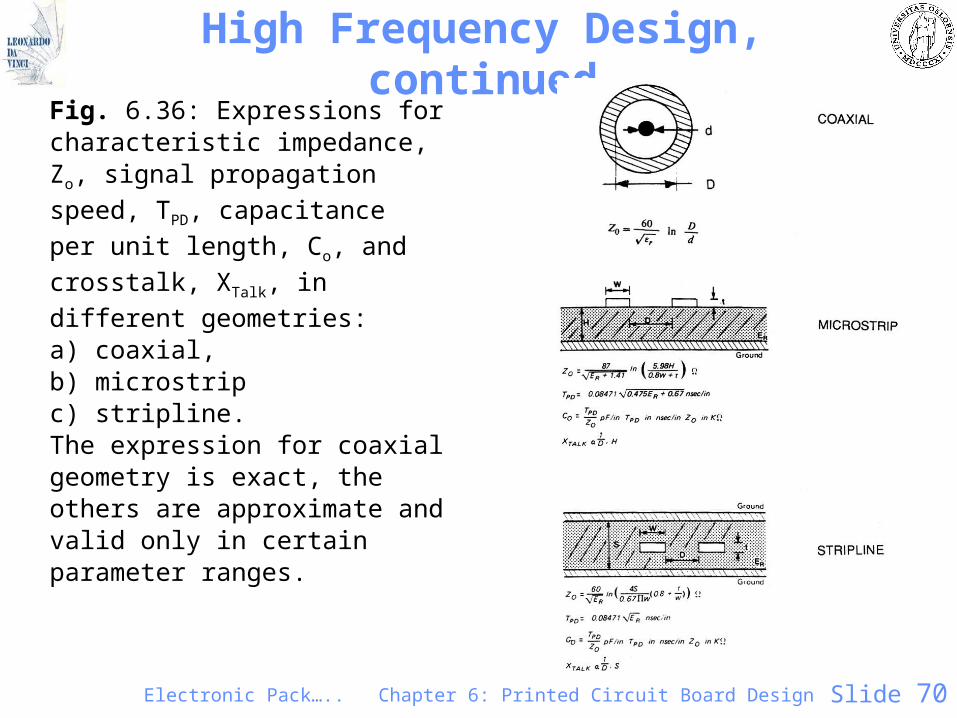
High Frequency Design, continuedFig. 6.36: Expressions for characteristic impedance, Zo,
signal propagation speed, TPD,
capacitance per unit length, Co,
and crosstalk, XTalk, in different
geometries: a) coaxial, b) microstrip c) stripline. The expression for coaxial geometry is exact, the others are approximate and valid only in certain parameter ranges.
Electronic Pack….. Chapter 6: Printed Circuit Board Design Slide 71
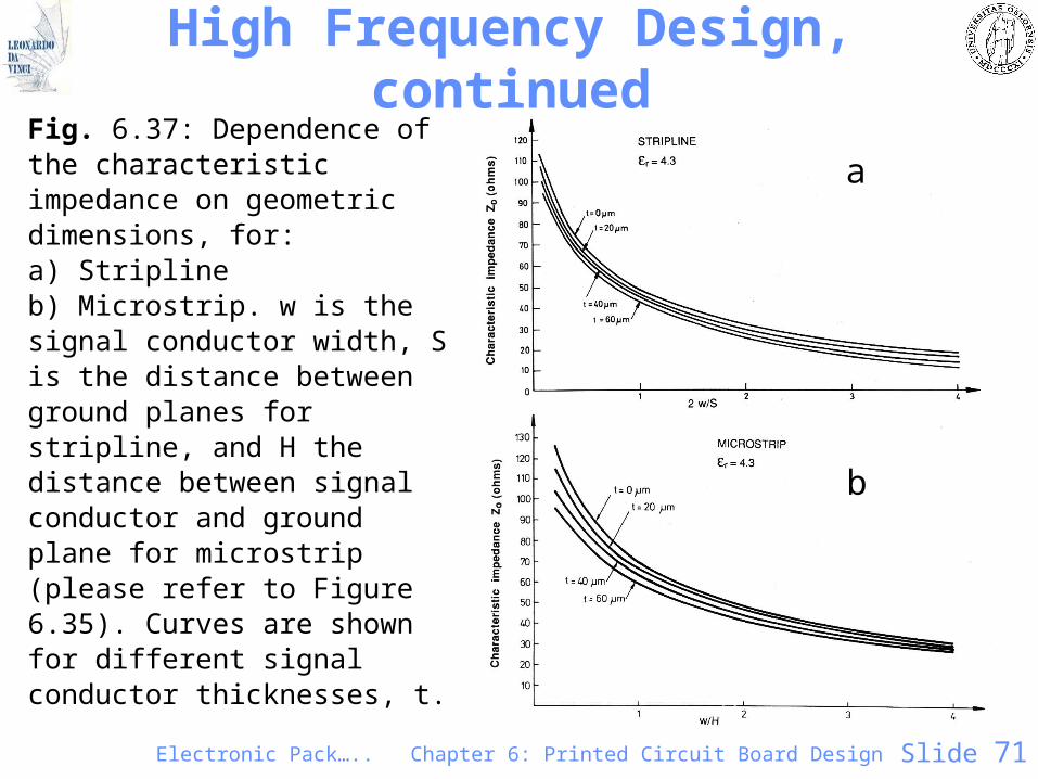
High Frequency Design, continued
Fig. 6.37: Dependence of the characteristic impedance on geometric dimensions, for: a) Striplineb) Microstrip. w is the signal conductor width, S is the distance between ground planes for stripline, and H the distance between signal conductor and ground plane for microstrip (please refer to Figure 6.35). Curves are shown for different signal conductor thicknesses, t.
a
b
72
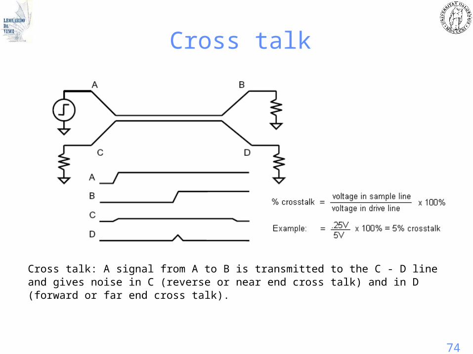
Cross talk
• Cross talk is the capacitive and inductive coupling of signals from one signal line to another
• Increases with board density and performance (frequency and current drive)– Distance to ground (power) plane– Smaller conductor spacing– Dielectric constant– Larger currents– Rise and fall times– Current drive
• Near End Crosstalk or reverse crosstalk If we measure the crosstalk in the sample line at the same end of the cable we inserted the signal, it is called near end or reverse/backward crosstalk.
• Far End Crosstalk or forward crosstalk If we measure the crosstalk in the sample line at the opposite end of the cable that we inserted the signal, it is called far end or forward crosstalk
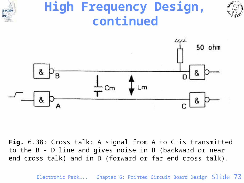
Electronic Pack….. Chapter 6: Printed Circuit Board Design Slide 73
High Frequency Design, continued
Fig. 6.38: Cross talk: A signal from A to C is transmitted to the B - D line and gives noise in B (backward or near end cross talk) and in D (forward or far end cross talk).
74
Cross talk
Cross talk: A signal from A to B is transmitted to the C - D line and gives noise in C (reverse or near end cross talk) and in D (forward or far end cross talk).
75
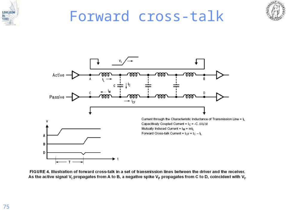
Forward cross-talk
76
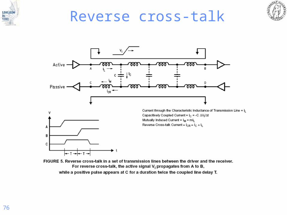
Reverse cross-talk
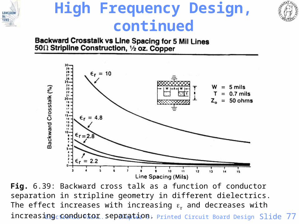
Electronic Pack….. Chapter 6: Printed Circuit Board Design Slide 77
High Frequency Design, continued
Fig. 6.39: Backward cross talk as a function of conductor separation in stripline geometry in different dielectrics. The effect increases with increasing r and
decreases with increasing conductor separation.
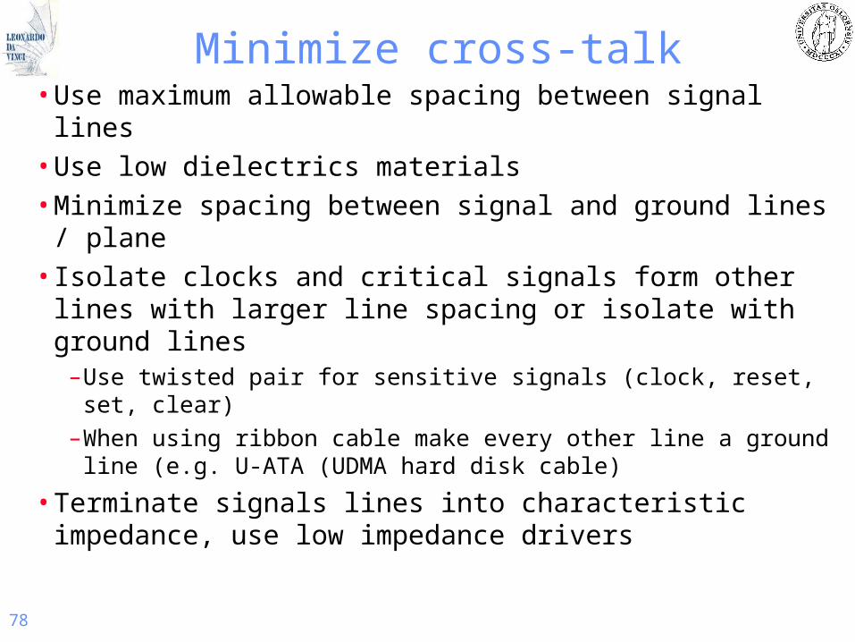
78
Minimize cross-talk• Use maximum allowable spacing between signal lines• Use low dielectrics materials• Minimize spacing between signal and ground lines /
plane• Isolate clocks and critical signals form other lines with
larger line spacing or isolate with ground lines– Use twisted pair for sensitive signals (clock, reset, set, clear)
– When using ribbon cable make every other line a ground line (e.g. U-ATA (UDMA hard disk cable)
• Terminate signals lines into characteristic impedance, use low impedance drivers
Electronic Pack….. Chapter 6: Printed Circuit Board Design Slide 79
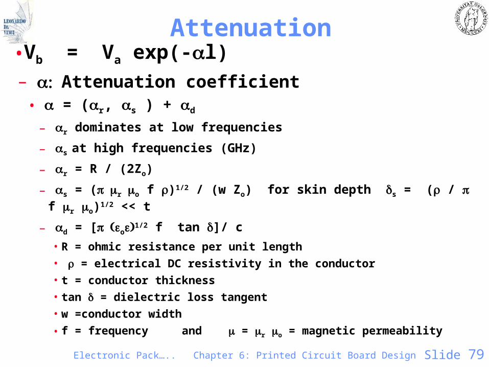
Attenuation•Vb = Va exp(-l)
– Attenuation coefficient• = (r, s ) + d
– r dominates at low frequencies
– s at high frequencies (GHz)
– r = R / (2Zo)
– s = (ro f )1/2 / (w Zo) for skin depth s = ( / f r o)1/2 << t
– d = [o1/2 f tan ]/ c
• R = ohmic resistance per unit length
• = electrical DC resistivity in the conductor
• t = conductor thickness
• tan = dielectric loss tangent
• w =conductor width
• f = frequency and = r o = magnetic permeability
80
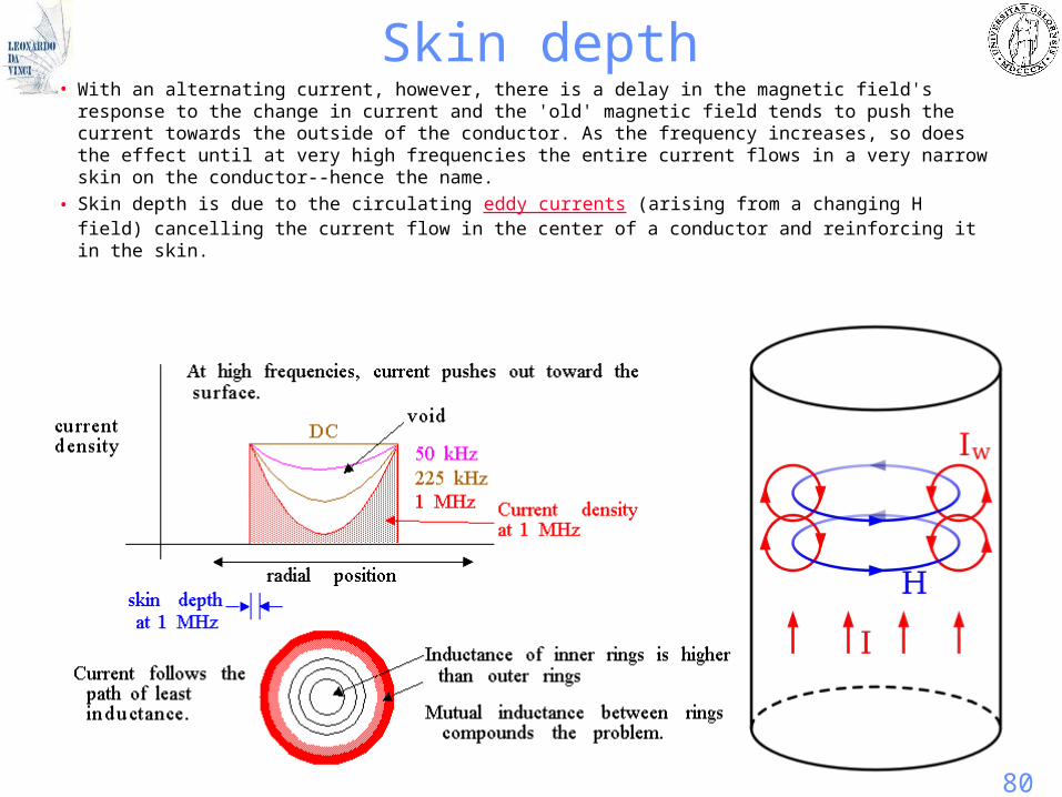
Skin depth• With an alternating current, however, there is a delay in the magnetic field's response to the
change in current and the 'old' magnetic field tends to push the current towards the outside of the conductor. As the frequency increases, so does the effect until at very high frequencies the entire current flows in a very narrow skin on the conductor--hence the name.
• Skin depth is due to the circulating eddy currents (arising from a changing H field) cancelling the current flow in the center of a conductor and reinforcing it in the skin.
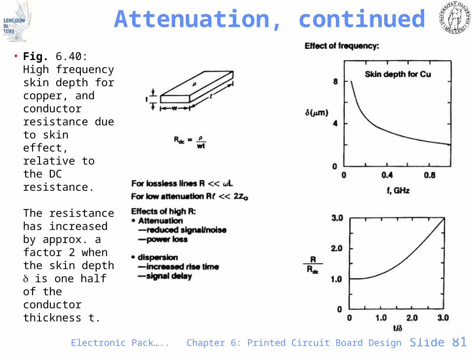
Electronic Pack….. Chapter 6: Printed Circuit Board Design Slide 81
Attenuation, continued
• Fig. 6.40: High frequency skin depth for copper, and conductor resistance due to skin effect, relative to the DC resistance.
The resistance has increased by approx. a factor 2 when the skin depth is one half of the conductor thickness t.
Electronic Pack….. Chapter 6: Printed Circuit Board Design Slide 82
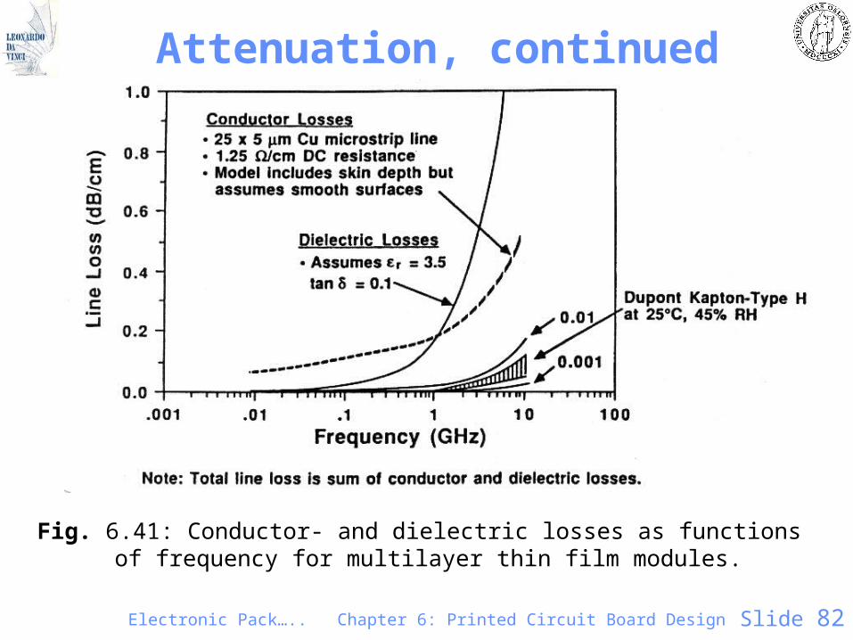
Attenuation, continued
Fig. 6.41: Conductor- and dielectric losses as functions of frequency for multilayer thin film modules.
83
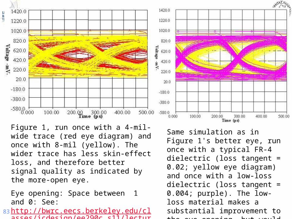
Same simulation as in Figure 1's better eye, run once with a typical FR-4 dielectric (loss tangent = 0.02; yellow eye diagram) and once with a low-loss dielectric (loss tangent = 0.004; purple). The low-loss material makes a substantial improvement to the eye opening, but would result in a much costlier PCB.
Figure 1, run once with a 4-mil-wide trace (red eye diagram) and once with 8-mil (yellow). The wider trace has less skin-effect loss, and therefore better signal quality as indicated by the more-open eye.
Eye opening: Space between 1 and 0: See: http://bwrc.eecs.berkeley.edu/classes/icdesign/ee290c_s11/lectures/Lecture02_Link_Over_Environ_6up.pdf
84
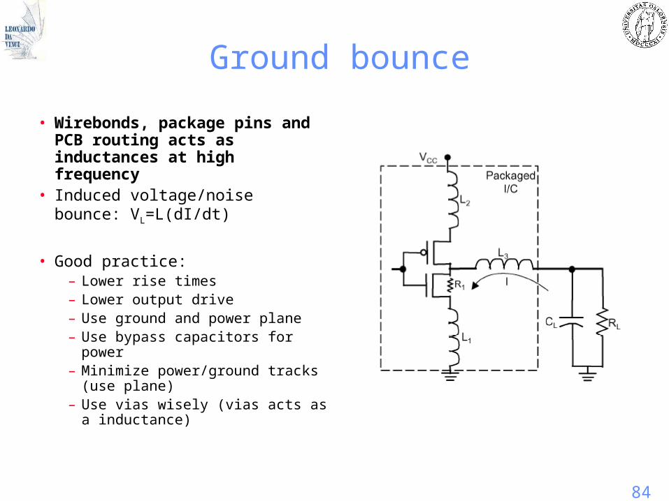
Ground bounce
• Wirebonds, package pins and PCB routing acts as inductances at high frequency
• Induced voltage/noise bounce: VL=L(dI/dt)
• Good practice:– Lower rise times– Lower output drive– Use ground and power plane– Use bypass capacitors for power– Minimize power/ground tracks (use
plane)– Use vias wisely (vias acts as a
inductance)
85
Power distribution
• Simultaneous switching gives large current spikes
• High capacitance Keeps stable voltage levels
• Low inductance makes L dI/dt switching noise low
• Power distribution is also modelled as transmission lines
• Reduced supply voltage reduced signal to noise
86
Practical • Use ground - power planes
– Reference planes for signal lines
– Better dynamic power distribution
• Time of flight– High packaging density
• Cross talk– Large separation between signal lines
• Want a high impedance from the driver circuit point of view: I= U/Z
• However: High impedance <=> Low packaging density
• Manufacturing tolerances
• Line width, homogeneity
87
EMC - Electromagnetic compliance
• International rules for:–Radiation of electromagnetic energy–Functionality of device in an electromagnetic field
(environment)
• Noise interference with other equipment
• Immunity against external radiation
• Design with respect to EMC/EMI from the start
88
EMC - Design of circuit
• Wires and current loops acts as antennas– Good PCB design– Ground and power planes
• Shielding• Basic design rules
– Ground plane– Compact design
• Reduced current loops• Minimum clock frequency
– Components with as long rise / fall time as possible– Decoupling capacitors– Shielding– Star topology– Metal case
LSots opening
89
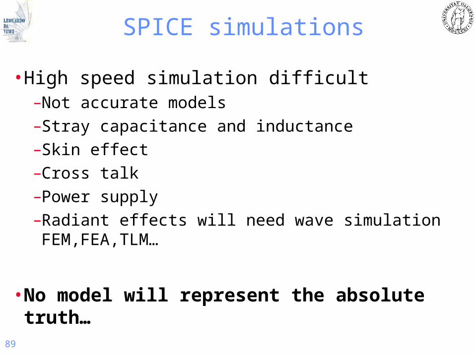
SPICE simulations
• High speed simulation difficult–Not accurate models–Stray capacitance and inductance–Skin effect–Cross talk–Power supply–Radiant effects will need wave simulation
FEM,FEA,TLM…
• No model will represent the absolute truth…

90
Software simulation at Ghz
• GREATER HIGH FREQUENCY CAUSE CONCERNS
• As Wave-lengths reduce to package pattern dimensions (@ 5 GHz , l/10 = 5 mm), each trace becomes a radiating antenna :
– Radiated energy = signal loss
– Radiated energy = interference on other electric conductors
– Radiated energy = increased EMC problems
– Radiated energy = damage to living organisms
• Alternative means of conduction will have to be used, when these factors become dangerous:
– Shielded conductors (conductor surrounded by Ground conductor)
– Wave-guides
– Light strands
• Full-wave Analysis becomes absolutely necessary
91
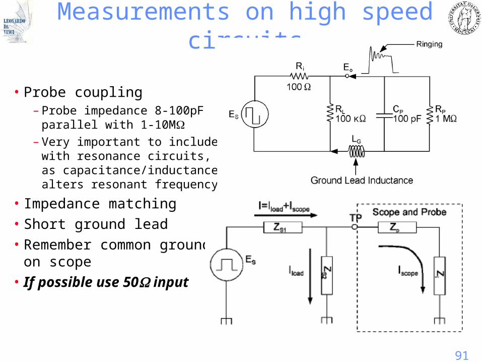
Measurements on high speed circuits
• Probe coupling– Probe impedance 8-100pF
parallel with 1-10M– Very important to include with
resonance circuits, as capacitance/inductance alters resonant frequency
• Impedance matching
• Short ground lead
• Remember common ground on scope
• If possible use 50 input
Electronic Pack….. Chapter 6: Printed Circuit Board Design Slide 92
Design of Flexible Printed Circuits
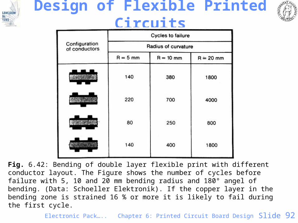
Fig. 6.42: Bending of double layer flexible print with different conductor layout. The Figure shows the number of cycles before failure with 5, 10 and 20 mm bending radius and 180° angel of bending. (Data: Schoeller Elektronik). If the copper layer in the bending zone is strained 16 % or more it is likely to fail during the first cycle.
Electronic Pack….. Chapter 6: Printed Circuit Board Design Slide 93
Design of Flexible Printed Circuits, continued
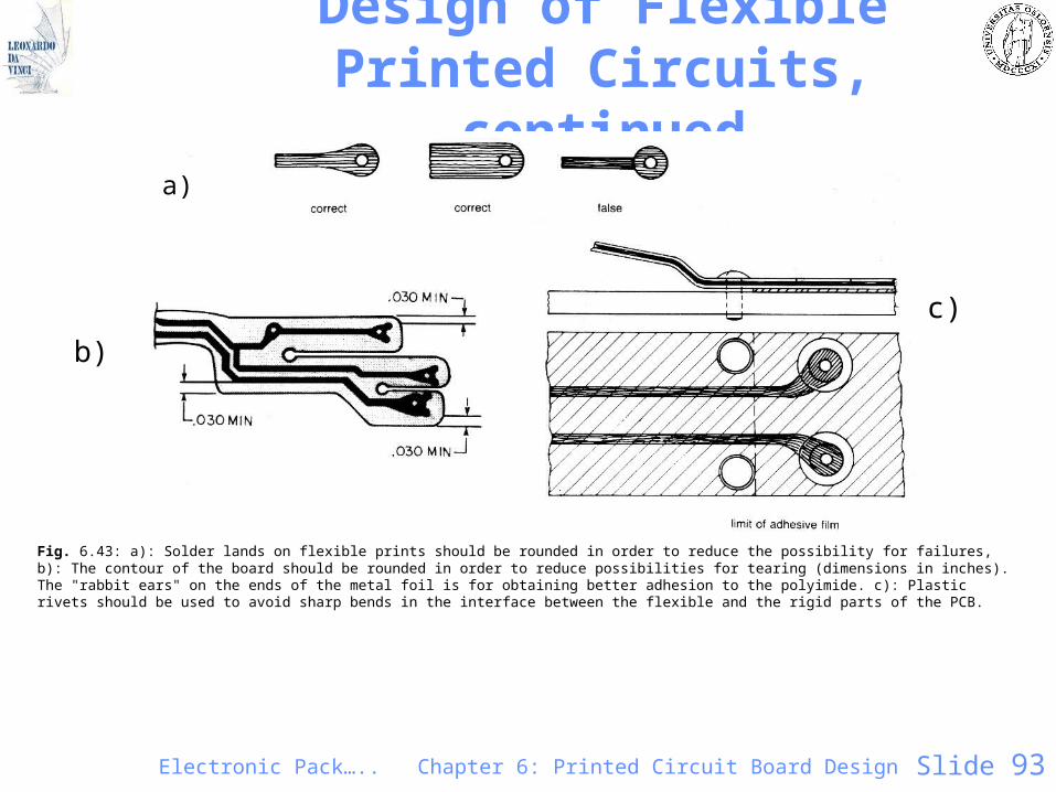
Fig. 6.43: a): Solder lands on flexible prints should be rounded in order to reduce the possibility for failures, b): The contour of the board should be rounded in order to reduce possibilities for tearing (dimensions in inches). The "rabbit ears" on the ends of the metal foil is for obtaining better adhesion to the polyimide. c): Plastic rivets should be used to avoid sharp bends in the interface between the flexible and the rigid parts of the PCB.
a)
b)
c)
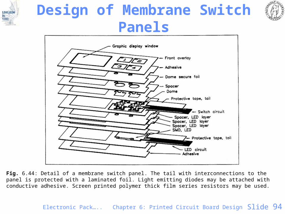
Electronic Pack….. Chapter 6: Printed Circuit Board Design Slide 94
Design of Membrane Switch Panels
Fig. 6.44: Detail of a membrane switch panel. The tail with interconnections to the panel is protected with a laminated foil. Light emitting diodes may be attached with conductive adhesive. Screen printed polymer thick film series resistors may be used.
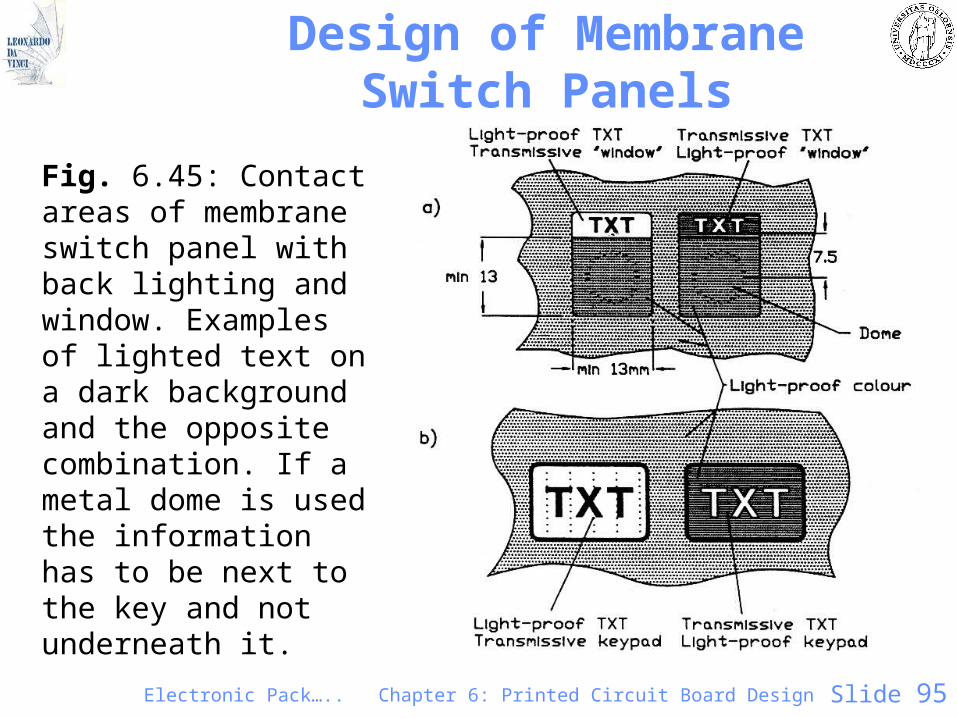
Electronic Pack….. Chapter 6: Printed Circuit Board Design Slide 95
Design of Membrane Switch Panels
Fig. 6.45: Contact areas of membrane switch panel with back lighting and window. Examples of lighted text on a dark background and the opposite combination. If a metal dome is used the information has to be next to the key and not underneath it.
Electronic Pack….. Chapter 6: Printed Circuit Board Design Slide 96
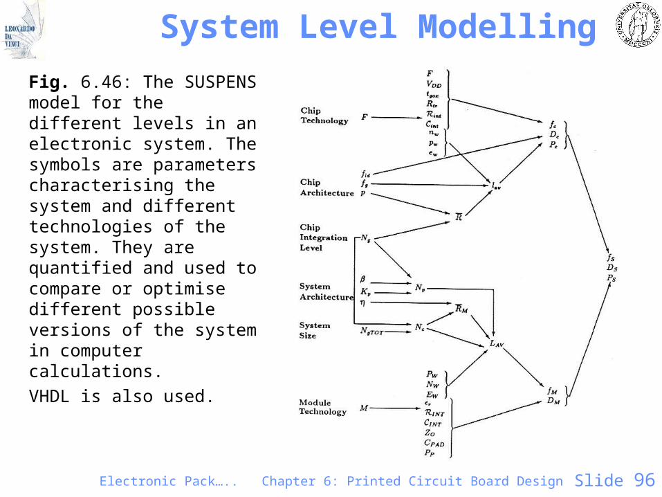
System Level Modelling
Fig. 6.46: The SUSPENS model for the different levels in an electronic system. The symbols are parameters characterising the system and different technologies of the system. They are quantified and used to compare or optimise different possible versions of the system in computer calculations.
VHDL is also used.
Electronic Pack….. Chapter 6: Printed Circuit Board Design Slide 97
End of Chapter 6: Printed Circuit Board Design
• Important issues:– When designing PCBs:
• Working with the right people including marketing and production people
• Working with the “best” tools– Use good Design Guidelines and do not violate
Design Parameters• Robust design to allow for process variations
– Use solder land dimension templates• Design for test• Specific design methods for applications with specific
requirements– High speed, high power etc.
• Questions and discussions?