Embed Size (px)
DESCRIPTION
Printed Circuit Board Design. Design Team 6 Alex Volinski Derek Brower Phil Jaworski Jung-Chung Lu Matt Affeldt. Introduction. Software Flow Routing / Board Layout Components/Assembly Electrical Considerations. Software Flow-Schematic. Software Packages Schematic Advantages - PowerPoint PPT Presentation
Citation preview
Printed Circuit Board Design
Design Team 6Alex Volinski
Derek BrowerPhil Jaworski
Jung-Chung LuMatt Affeldt
Software Flow Routing / Board Layout Components/Assembly Electrical Considerations
Introduction
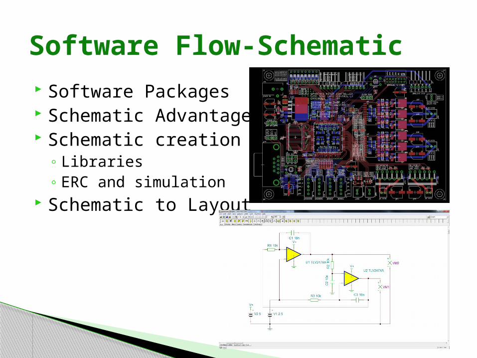
Software Packages Schematic Advantages Schematic creation
◦ Libraries◦ ERC and simulation
Schematic to Layout
Software Flow-Schematic
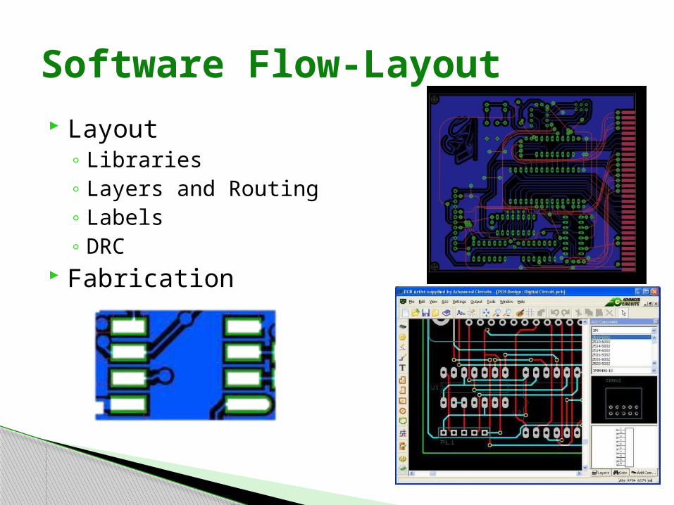
Layout◦ Libraries◦ Layers and Routing◦ Labels◦ DRC
Fabrication
Software Flow-Layout
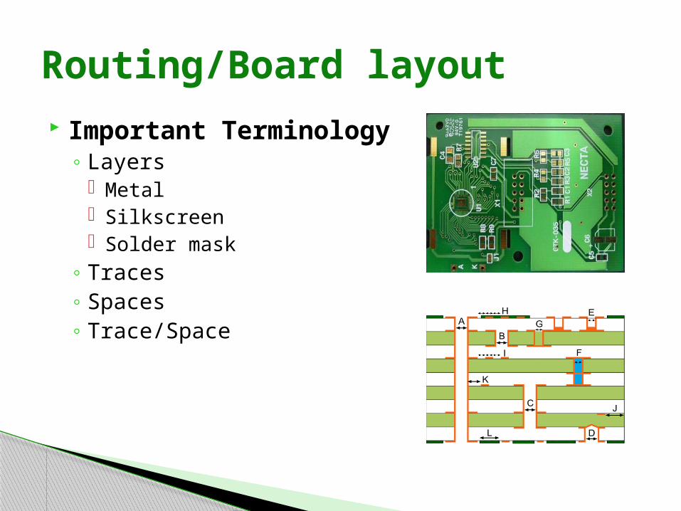
Important Terminology◦ Layers
Metal Silkscreen Solder mask
◦ Traces◦ Spaces◦ Trace/Space
Routing/Board layout
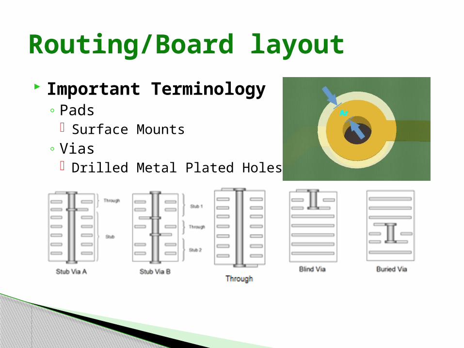
Important Terminology◦ Pads
Surface Mounts◦ Vias
Drilled Metal Plated Holes
Routing/Board layout
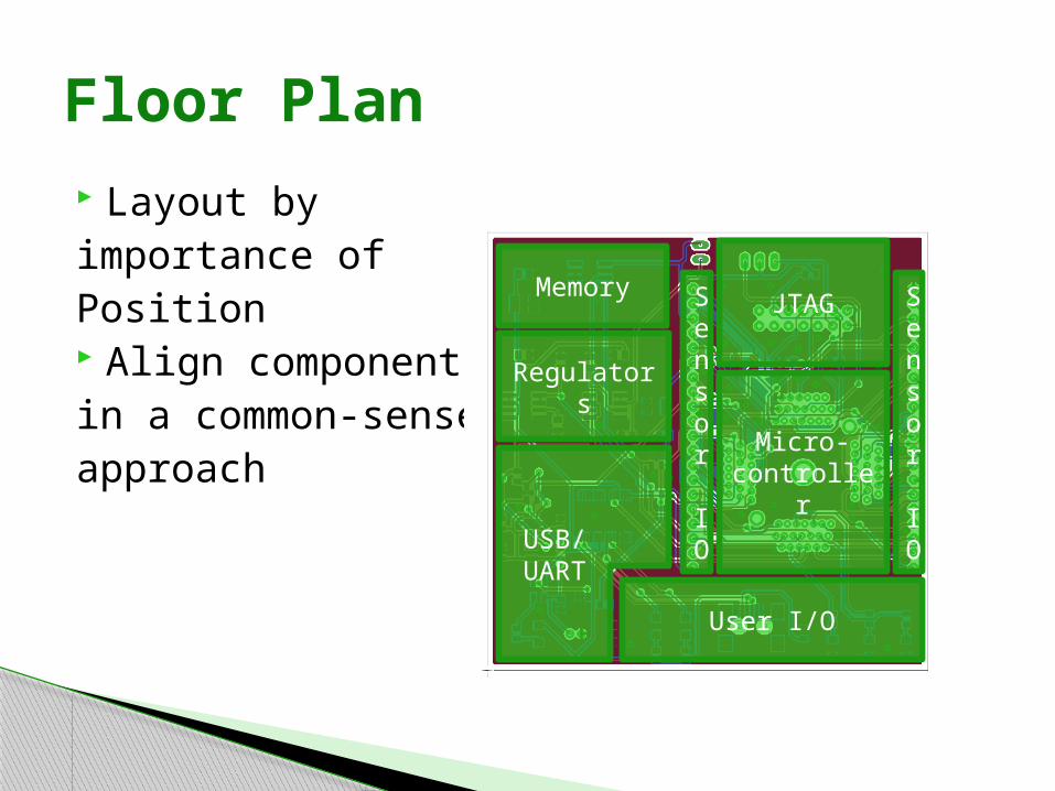
Layout by importance of Position Align componentsin a common-senseapproach
Floor Plan
Regulators
Sensor IO
Sensor IO
Memory
User I/O
Micro-controller
JTAG
USB/UART
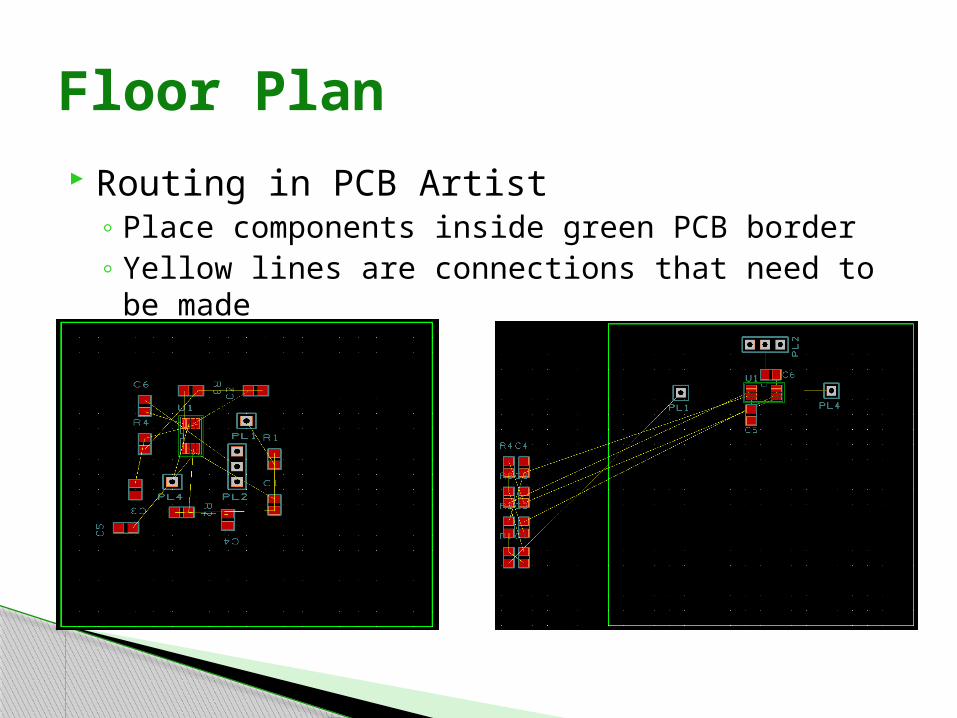
Routing in PCB Artist◦ Place components inside green PCB border◦ Yellow lines are connections that need to be made
Floor Plan
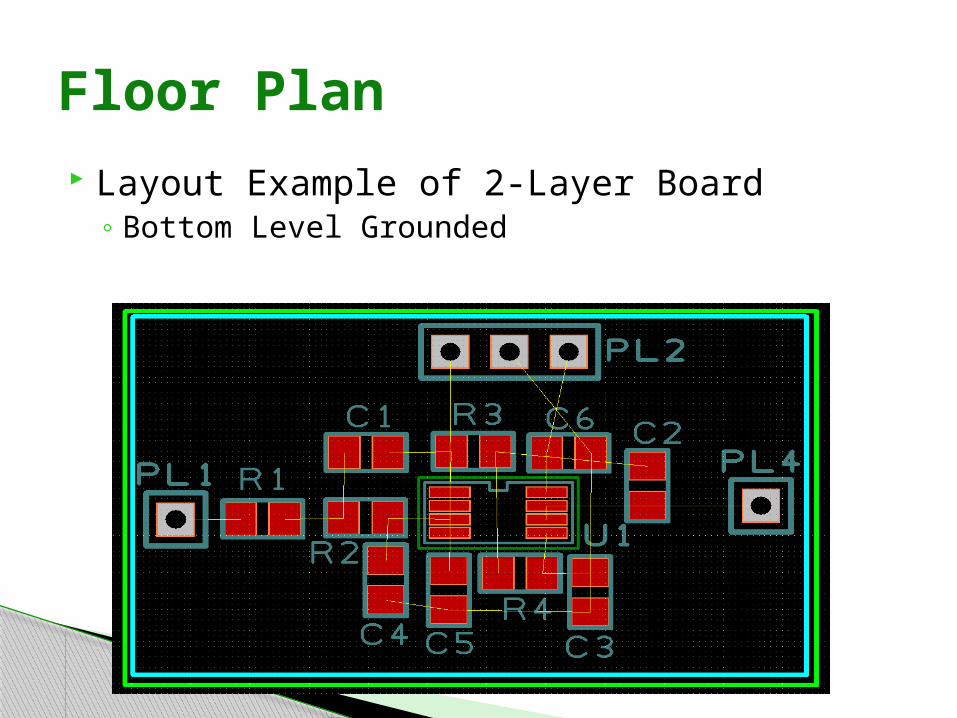
Floor Plan Layout Example of 2-Layer Board
◦ Bottom Level Grounded
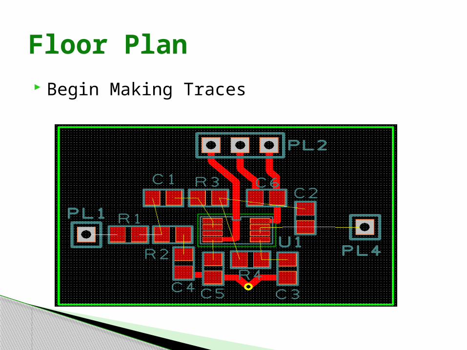
Floor Plan Begin Making Traces
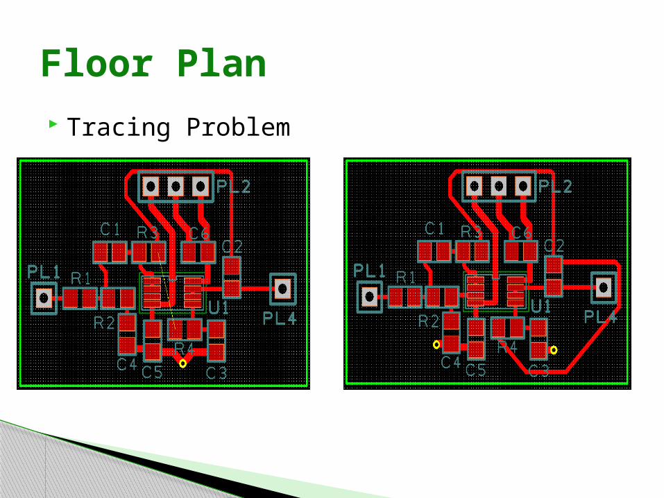
Tracing Problem
Floor Plan
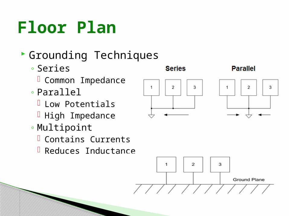
Grounding Techniques◦ Series
Common Impedance◦ Parallel
Low Potentials High Impedance
◦ Multipoint Contains Currents Reduces Inductance
Floor Plan
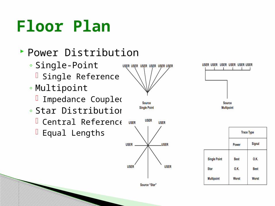
Power Distribution◦ Single-Point
Single Reference◦ Multipoint
Impedance Coupled◦ Star Distribution
Central Reference Equal Lengths
Floor Plan
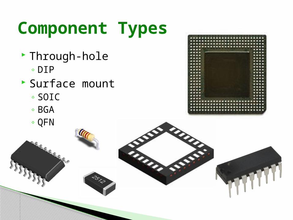
Through-hole◦ DIP
Surface mount◦ SOIC◦ BGA◦ QFN
Component Types
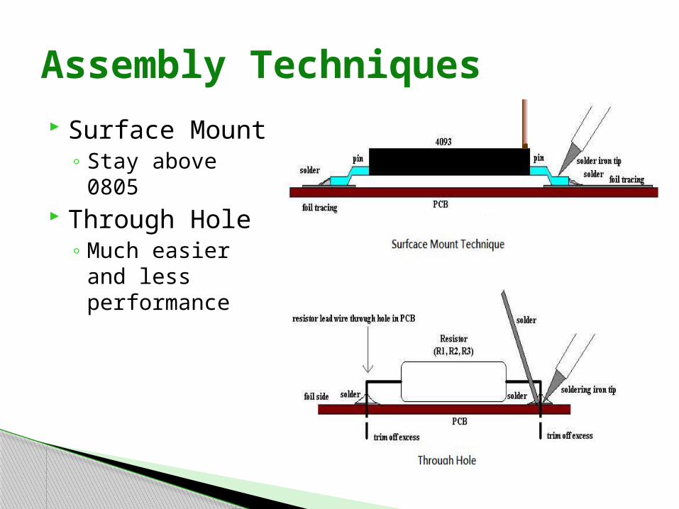
Surface Mount◦ Stay above 0805
Through Hole◦ Much easier and
less performance
Assembly Techniques
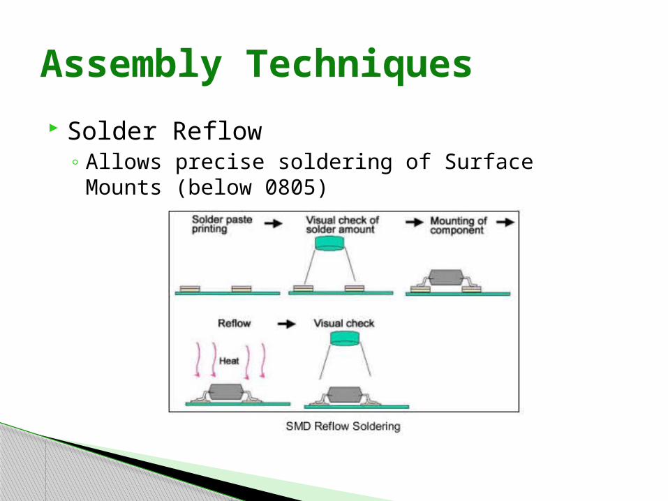
Solder Reflow◦ Allows precise soldering of Surface Mounts (below
0805)
Assembly Techniques
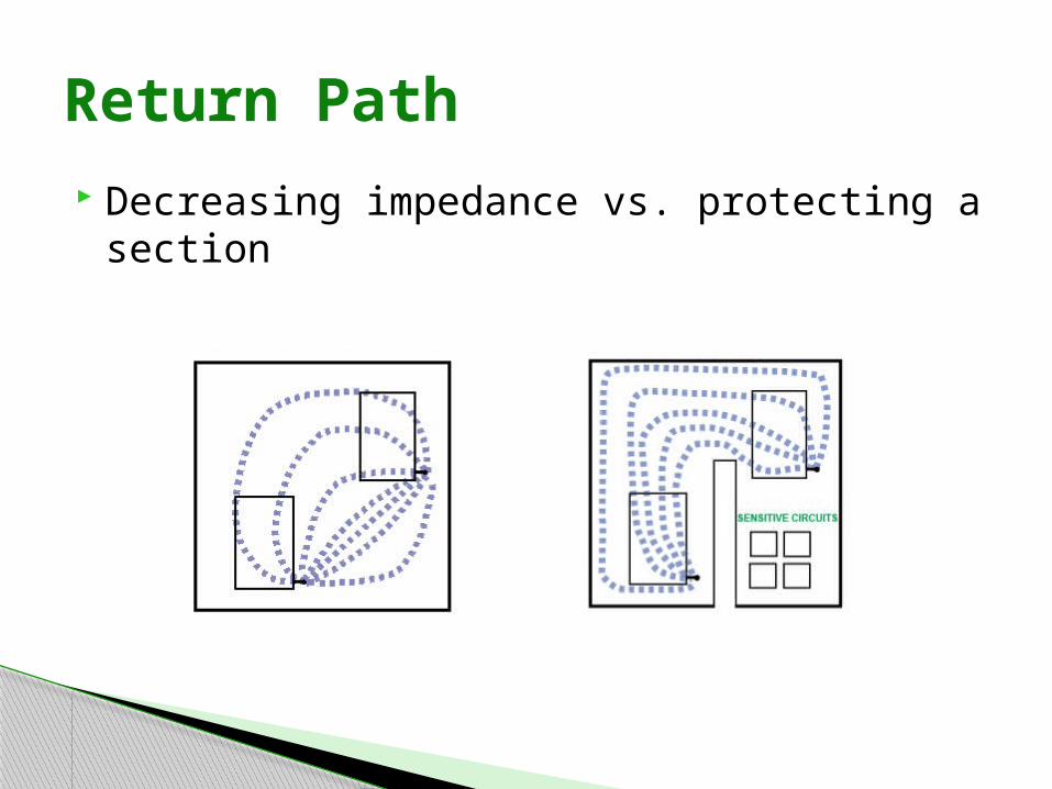
Decreasing impedance vs. protecting a section
Return Path
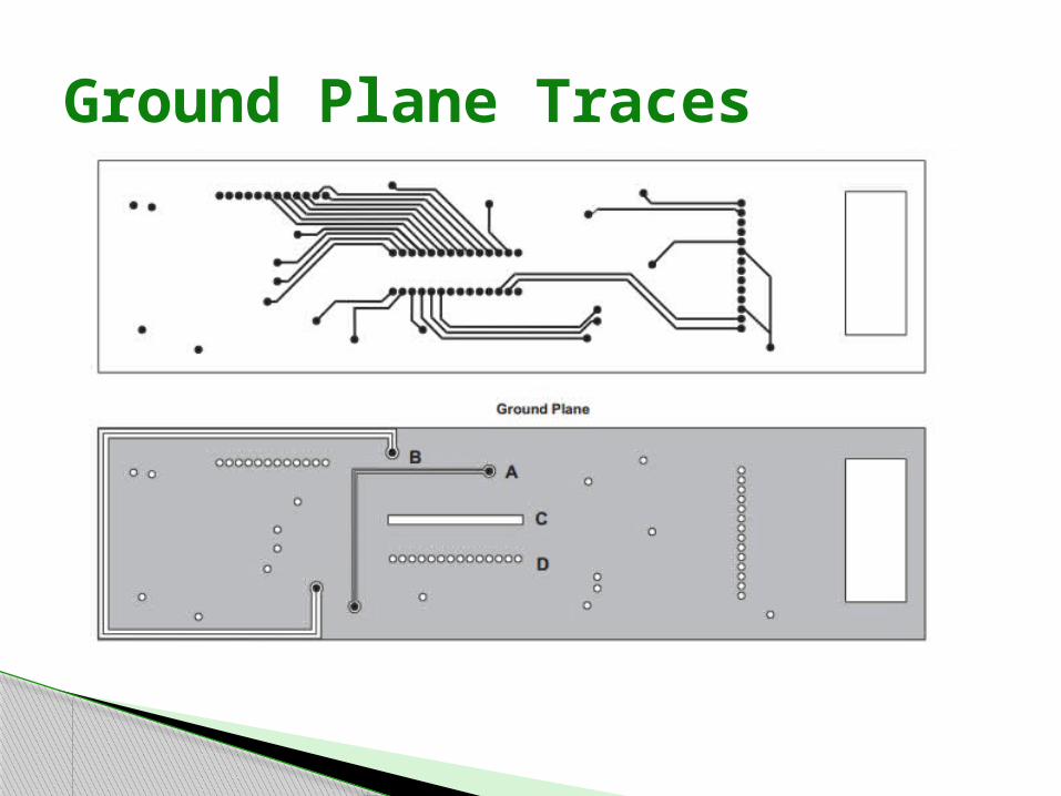
Ground Plane Traces
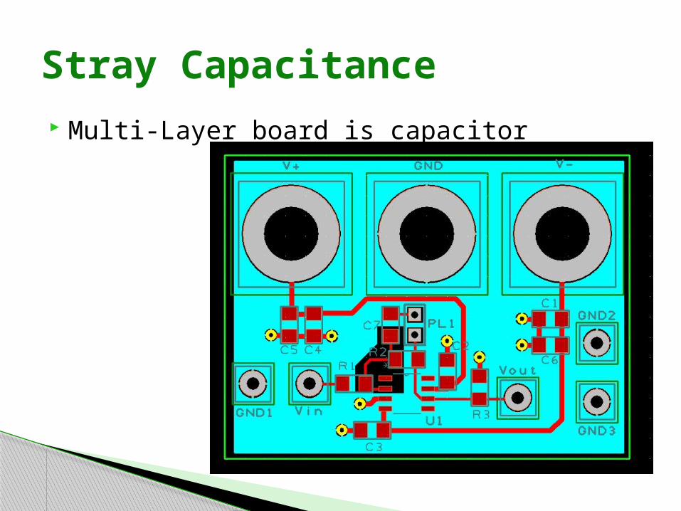
Multi-Layer board is capacitor
Stray Capacitance
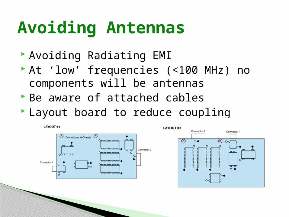
Avoiding Radiating EMI At ‘low’ frequencies (<100 MHz) no
components will be antennas Be aware of attached cables Layout board to reduce coupling
Avoiding Antennas
Software Flow◦ Advantage of making schematic◦ Layers, Libraries, Fabrication
Routing / Board Layout◦ Layers, Traces, Pads vs. Vias◦ Importance of position◦ Grounding Techniques, Power Distribution
Conclusion
Components/Assembly◦ Different types of components◦ Through Hole / Surface Mount◦ Weighing options for better performance
Electrical considerations◦ Stray Capacitance ◦ Ground Plane Traces◦ Antennas to avoid radiating EMI
Conclusion

Questions