Embed Size (px)
Citation preview

Efficiency Enhancement of Pico-cell Base Station Power Amplifier MMIC in GaN HFET Technology
Using the Doherty technique
Sashieka Seneviratne
A thesis presented to Ottawa Carleton Institute for Electrical and Computer Engineering
in partial fulfillment to the thesis requirement for the degree of
MASTER OF APPLIED SCIENCE
in
ELECTRICAL ENGINEERING
University of Ottawa
Ottawa, Ontario, Canada
June 2012
© Sashieka Seneviratne, Ottawa, Canada, 2012

Abstract 1
Abstract
With the growth of smart-phones, the demand for more broadband, data-centric tech-
nologies are being driven higher. As mobile operators worldwide plan and deploy 4th genera-
tion (4G) networks such as LTE to support the relentless growth in mobile data demand, the
need for strategically positioned pico-sized cellular base stations known as ‘pico-cells’ are
gaining traction. In addition to having to design a transceiver in a much compact footprint,
pico-cells must still face the technical challenges presented by the new 4G systems, such as
reduced power consumptions and linear amplification of the signals.
The RF power amplifier (PA) that amplifies the output signals of 4G pico-cell systems face
challenges to minimize size, achieve high average efficiencies and broader bandwidths while
maintaining linearity and operating at higher frequencies. 4G standards as LTE use non-
constant envelope modulation techniques with high peak to average ratios. Power amplifiers
implemented in such applications are forced to operate at a backed off region from satura-
tion. Therefore, in order to reduce power consumption, a design of a high efficiency PA that
can maintain the efficiency for a wider range of radio frequency signals is required.
The primary focus of this thesis is to enhance the efficiency of a compact RF amplifier suita-
ble for a 4G pico-cell base station. For this aim, an integrated two way Doherty amplifier de-
sign in a compact 10x11.5mm2 monolithic microwave integrated circuit using GaN device
technology is presented. Using non-linear GaN HFETs models, the design achieves high effi-
ciencies of over 50% at both back-off and peak power regions without compromising on the
stringent linearity requirements of 4G LTE standards. This demonstrates a 17% increase in
power added efficiency at 6 dB back off from peak power compared to conventional Class
AB amplifier performance. Performance optimization techniques to select between high effi-
ciency and high linearity operation are also presented.
Overall, this thesis demonstrates the feasibility of an integrated HFET Doherty amplifier for
LTE band 7 which entails the frequencies from 2.62-2.69GHz. The realization of the layout
and various issues related to the PA design is discussed and attempted to be solved.

Acknowledgment 2
Acknowledgment
This thesis would not have been possible without the support of a number of people. The au-
thor would like to take this opportunity to express her deep gratitude to them.
First and foremost, I would like to convey my gratitude to my parents Nandinie and Gamini
Seneviratne. Without their encouragement it would have been impossible to find the energies
to complete this endeavour.
I would also like to thank my husband. I cannot express in words my appreciation to him for
accepting my endeavours and whose dedication, love and persistent confidence in me, has
given me the strength to complete this research.
My deepest gratitude is also owed to my co-supervisor Dr. Rony Amaya for all his patience,
advice, supervision, crucial contributions and his eagerness to share his wealth of knowledge
with me.
Lastly, I would like to give special thanks to my supervisor, Dr. Mustapha Yagoub, for all his
for his supervision, advice, and guidance which was vital in the completion of the thesis.
Above all and the most needed, his unflinching encouragement and support in various ways
to inspire and enrich my growth as a researcher to complete this research.
I will always be indebted to all of these extraordinary people.

Table of Contents 3
Table of Contents
ABSTRACT ........................................................................................................................................................... 1
ACKNOWLEDGMENT ....................................................................................................................................... 2
TABLE OF CONTENTS ...................................................................................................................................... 3
LIST OF FIGURES ............................................................................................................................................... 5 LIST OF TABLES ................................................................................................................................................. 7
LIST OF ACRONYMS AND ABBREVIATIONS ............................................................................................. 8
CHAPTER 1 INTRODUCTION ....................................................................................................................... 9 1.1 MOTIVATIONS ................................................................................................................................................ 9 1.2 BACKGROUND: POWER AMPLIFIER DESIGN CHALLENGES FOR PICO-CELLS ................................................. 10
1.2.1 Addressing Linearity challenges ......................................................................................................... 11 1.2.2 Addressing average efficiency challenges .......................................................................................... 11 1.2.3 Addressing design space challenges ................................................................................................... 12
1.3 RESEARCH GOALS ....................................................................................................................................... 12 1.4 THESIS ORGANIZATION ................................................................................................................................ 13
CHAPTER 2 BASICS OF RF POWER AMPLIFIER DESIGN .................................................................. 14 2.1 CLASSES OF OPERATION IN RF POWER AMPLIFIERS .................................................................................... 14
2.1.1 Class A ................................................................................................................................................ 16 2.1.2 Class B ................................................................................................................................................ 17 2.1.3 Class AB ............................................................................................................................................. 18 2.1.4 Class C ................................................................................................................................................ 18 2.1.5 Additional power Classes .................................................................................................................... 19
2.2 POWER AMPLIFIER PERFORMANCE METRICS ............................................................................................... 19 2.2.1 Stability ............................................................................................................................................... 20 2.2.2 1 dB Compression point (P1dB) and Psat ............................................................................................. 21 2.2.3 Efficiency ............................................................................................................................................ 22 2.2.4 Linearity .............................................................................................................................................. 23
2.3 EFFICIENCY ENHANCEMENT TECHNIQUES ................................................................................................... 25 2.3.1 Envelope elimination and restoration (EER)....................................................................................... 26 2.3.2 Envelope tracking (ET) ....................................................................................................................... 27 2.3.3 Chireix Outphasing ............................................................................................................................. 28 2.3.4 Doherty Amplification Technique ...................................................................................................... 29
2.4 POWER AMPLIFIER TOPOLOGY SELECTION .................................................................................................. 33 2.5 DOHERTY OPERATION ................................................................................................................................. 35
2.5.1 Doherty load modulation technique .................................................................................................... 35 2.5.2 Doherty Amplifier Operation .............................................................................................................. 41
2.6 CONCLUSION ............................................................................................................................................... 47
CHAPTER 3 SEMICONDUCTOR TECHNOLOGY SELECTION AND GAN LARGE-SIGNAL MODEL EVALUATION .................................................................................................................................... 48
3.1 SEMICONDUCTOR TECHNOLOGY SELECTION................................................................................................ 48 3.1.1 GaN properties .................................................................................................................................... 49 3.1.2 GaN issues and limitations .................................................................................................................. 52

Table of Contents 4
3.1.3 GaN MMIC processs ........................................................................................................................... 53 3.2 CONCLUSION ............................................................................................................................................... 54 3.3 TRANSISTOR MODEL EVALUATION WITH A SINGLE STAGE GAN PA DESIGN USING CGH25120F ................ 55
3.3.1 DC analysis ......................................................................................................................................... 56 3.3.2 CGH25120F evaluation board matching network analysis ................................................................. 59 3.3.3 Comparison of Measured and Simulated Performance of CGH25120F ............................................. 65
CHAPTER 4 DOHERTY POWER AMPLIFIER DESIGN IMPLEMENTATION & RESULTS ........... 70 4.1 DOHERTY AMPLIFIER DESIGN FOR A 5W PICO-CELL BASE STATION ............................................................ 70
4.1.1 Design Specifications for LTE ............................................................................................................ 70 4.1.2 Design procedure ................................................................................................................................ 72 4.1.3 Device Sizing ...................................................................................................................................... 73 4.1.4 DC analysis ......................................................................................................................................... 74 4.1.5 Main and peaking amplifier design ..................................................................................................... 76 4.1.5.1 Optimum load selection ................................................................................................................... 76 4.1.5.2 Main and Peak amplifier matching network design and verification ............................................... 76 4.1.6 Bias network design ............................................................................................................................ 83 4.1.6.1 Quarter wave feed with a shunt RF resonant capacitor .................................................................... 83 4.1.6.2 Quarter wave feed with a radial stub ................................................................................................ 84 4.1.6.3 Lumped element bias network ......................................................................................................... 85 4.1.7 Doherty Combiner design ................................................................................................................... 85 4.1.8 Implementation ................................................................................................................................... 86 4.1.9 Layout design ...................................................................................................................................... 89 4.1.9.1 Passive Components ......................................................................................................................... 89 4.1.9.2 Bonding Pads ................................................................................................................................... 90 4.1.9.3 Bias circuit ....................................................................................................................................... 91 4.1.9.4 Layout input and output matching networks .................................................................................... 92 4.1.9.5 Doherty combiner layout .................................................................................................................. 95 4.1.9.6 Complete Doherty amplifier layout .................................................................................................. 97
4.2 DOHERTY AMPLIFIER PERFORMANCE EVALUATION..................................................................................... 98 4.2.1 Large signal single tone simulations ................................................................................................... 98 4.2.2 Large signal two tone simulations ..................................................................................................... 101 4.2.3 Thermal dissipation ........................................................................................................................... 103 4.2.4 Performance Optimization ................................................................................................................ 104 4.2.4.1 Main and peaking amplifier bias optimization ............................................................................... 104 4.2.5 Full LTE band-7 over frequency performance summary .................................................................. 108
CHAPTER 5 CONCLUSION AND FUTURE WORK ............................................................................... 111
5.1 SUMMARY .................................................................................................................................................. 111 5.2 CONCLUSION ............................................................................................................................................. 112 5.3 FUTURE WORK .......................................................................................................................................... 112
REFERENCES .................................................................................................................................................. 114
APPENDIX A: CGH25120F EVALUATION BOARD .................................................................................. 121
APPENDIX B: SIMULATION TEST BENCH AND RESULTS OF CGH25120F ..................................... 123
APPENDIX C: MEASUREMENT SETUP FOR CGH25120F ..................................................................... 126
List of Figures 5
List of Figures
Figure 1: Load lines of various power amplifier classes of operation ................................................... 14 Figure 2: (a), (b) Classes of operation of Power amplifiers and their standard definition [31] ............. 15 Figure 3: Class A transfer characteristic [32] ........................................................................................ 16 Figure 4: Class B transfer characteristic [32] ........................................................................................ 18 Figure 5: Class AB transfer characteristic [32] ..................................................................................... 19 Figure 6: 1 dB Compression point (P1dB) and Psat .............................................................................. 22 Figure 7: Frequency spectrum of a two-tone signal .............................................................................. 24 Figure 8: Second and third-order intercept points ................................................................................. 25 Figure 9: Envelope elimination and restoration (EER) system block diagram [35] .............................. 27 Figure 10: Envelope Tracking (ET) system block diagram................................................................... 28 Figure 11: Doherty amplifier block diagram ......................................................................................... 29 Figure 12: Efficiency of a conventional symmetrical Doherty PA compared to a class B PA [82]. ..... 31 Figure 13: Efficiency behavior of N-stage and asymmetric Doherty PA architectures compared to
Class B PA [39] ............................................................................................................................ 33 Figure 14: Theoretical efficiency behavior of various efficiency enhancement techniques [83]. ......... 35 Figure 15: Active load modulation technique ....................................................................................... 36 Figure 16: Operational diagram of the Doherty amplifier ..................................................................... 37 Figure 17: Main and peaking device currents Vs input voltage amplitude ........................................... 39 Figure 18: Doherty low power operation diagram ................................................................................ 43 Figure 19: Doherty amplifier efficiency Vs input drive level ............................................................... 43 Figure 20: Doherty medium power operation diagram ......................................................................... 44 Figure 21: Main and peaking device voltages Vs input voltage amplitude ........................................... 45 Figure 22: Doherty high power operation diagram ............................................................................... 46 Figure 23: Doherty amplifier efficiency Vs power back off ................................................................. 46 Figure 24: Comparison of highest reported ft and fmax for different RF device technologies [50] ..... 54 Figure 25: Comparison of RF power density for different RF device technologies [50] ...................... 55 Figure 26: CGH25120F large signal transistor model’s transfer characteristic .................................... 57 Figure 28: DC output characteristics of CGH25120F ........................................................................... 58 Figure 29: Test bench for DC analysis of Cree’s CGH25120F large signal transistor model .............. 58 Figure 30: ADS schematic of CGH25120F evaluation board matching networks ; (a) input matching
(b) output matching ....................................................................................................................... 61 Figure 31: Layout of CGH25120F evaluation board input matching network with bias feeds ............. 62 Figure 32: Layout of CGH25120F evaluation board output matching network with bias feeds ........... 62 Figure 33: Simulated efficiency and power delivered Load-pull contours at the load impedance from
the simulated momentum structures for CGH25120F evaluation board ...................................... 64 Figure 34: Simulated IMD3, efficiency and power delivered Load-pull contours from the simulated
momentum structures for CGH25120F evaluation board ............................................................. 65 Figure 35: Measurement setup of CGH25120F evaluation board ......................................................... 66 Figure 36: Measured and simulated compression curves for CGH25120F ........................................... 68 Figure 37: Measured and simulated gain over frequency for CGH25120F .......................................... 68 Figure 38: Measured and simulated drain efficiency over frequency for CGH25120F ........................ 69 Figure 39: Doherty Amplifier design blocks ......................................................................................... 73 Figure 40: Transfer characteristic for two 8 x 200µm HFETs at 20V drain voltage ............................. 75

List of Figures 6
Figure 41: I-V curves for two 8 x 200µm HFETs.................................................................................. 75 Figure 42: Power added efficiency and power delivered contours with Vds=20V and Vgs=-3.0V ...... 77 Figure 43: Simulated load impedances with Vds=20V and Vgs=-3.0V ................................................ 77 Figure 44: Quarter wave transmission line equivalent model ................................................................ 78 Figure 45: Input matching network with ideal components................................................................... 78 Figure 46: Output matching network with ideal components ................................................................ 79 Figure 47: Input and output matching networks with foundry schematic elements .............................. 80 Figure 48: Main amplifier single-tone simulations at Vdd =20V, Vgs= -3.0V, (a) Output power Vs
gain, (b) Output power Vs Power added efficiency .................................................................... 81 Figure 49: Peak amplifier single-tone simulations at Vdd =20V, Vgs= -4.9V, (a) Output power Vs
gain, (b) Output power Vs Power added efficiency ..................................................................... 82 Figure 50: Radian stub ........................................................................................................................... 84 Figure 51: Radial stub section ................................................................................................................ 84 Figure 52: Doherty Output combiner ..................................................................................................... 86 Figure 53: Schematic of the Doherty power amplifier ........................................................................... 88 Figure 54: MIM capacitor layout ........................................................................................................... 89 Figure 55: Spiral inductor layout ........................................................................................................... 90 Figure 56: RF bond pads ........................................................................................................................ 91 Figure 57: DC bond pads ....................................................................................................................... 91 Figure 58: Layout design of bias circuit ................................................................................................ 92 Figure 59: Tuned input matching equivalent circuit .............................................................................. 92 Figure 60: Schematic input and output matching networks ................................................................... 94 Figure 62: Doherty combiner layout ...................................................................................................... 95 Figure 63: Doherty combiner verification ............................................................................................. 96 Figure 64: Verification of layout design of the Doherty combiner ........................................................ 96 Figure 65: Layout of the designed MMIC Doherty amplifier ................................................................ 97 Figure 66: Simulated small signal transmission and reflection coefficients of the 5W Doherty
Amplifier ....................................................................................................................................... 99 Figure 67: Single tone simulations with Vdrain=20V, Vgs_main=-3.0V,Vgs_peak=-4.9V (a) Power
added efficiency of the Doherty amplifier (b) Gain of the Doherty amplifier (c) Comparison of Power added efficiencies of Class AB and Doherty amplifiers .................................................. 101
Figure 68: Two tone simulations with Vdrain=20V, Vgs_main=-3.0V,Vgs_peak=-4.9V (a) IMD3 Vs output power of the Doherty amplifier (b) IMD5 Vs output power of the Doherty amplifier ... 102
Figure 69: Doherty amplifier optimization with main amplifier bias variation (a) PAE response of Doherty amplifier with variation in main amplifier bias (b) Gain response of Doherty amplifier with variation in main amplifier bias .......................................................................................... 105
Figure 70: Doherty amplifier optimization with peaking stage bias variation (a)PAE response of Doherty amplifier with variation in peaking amplifier bias (b) Gain of the Doherty amplifier with variation in peaking amplifier bias (c) IMD3 response of Doherty am ............................. 107
Figure 71: Simulated over Frequency performance of the Doherty Amplifier with Vdrain=20V, Vgs_main=-3.0V,Vgs_peak=-4.9V (a) Over frequency PAE % of the designed MMIC Doherty Amplifier ..................................................................................................................................... 109
Figure 72: Tested CGH25120F evaluation board ................................................................................ 121 Figure 73: Datasheet image of CGH25120F evaluation board [54] .................................................... 122 Figure 74: CGH25120F evaluation board simulated gain compression curve at 2.650GHz ............... 123 Figure 75: CGH25120F evaluation board simulated current consumption Vs output power at
2.650GHz .................................................................................................................................... 124 Figure 76: CGH25120F evaluation board co- simulation test bench ................................................... 125 Figure 77: Measurement setup for CGH25120F .................................................................................. 126

List of Tables 7
List of Tables
Table 1: Semiconductor material properties and their relationship with power amplifier system performance [50]. ......................................................................................................................... 50
Table 2: Material Properties of GaN, Si and GaAs [50]........................................................................ 50 Table 3: Comparison of measured and simulated impedances of CGH25120F .................................... 63 Table 4: Measured and simulated performance data of the CGH25120F evaluation board .................. 66 Table 5: Design requirements ................................................................................................................ 71 Table 6: Main and peaking amplifier gate bias voltages for class AB and class C operation ............... 76 Table 7: Input matching components before and after tuning ............................................................... 93 Table 8: Output matching components after and before tuning ............................................................ 93 Table 9: Layout and schematic class AB performance summary .......................................................... 93 Table 10: Thermal dissipation and total current draw of the Doherty PA ........................................... 103 Table 11: Full LTE band-7 performance summary of the MMIC Doherty Amplifier ........................ 108 Table 12: Performance comparison of the designed Doherty PA to published MMIC PAs ............... 110

List of Acronyms and Abbreviations 8
List of Acronyms and Abbreviations
3GPP Third generation partnership project 4G Fourth Generation ACLR Adjacent Channel Leakage Ratio ACPR Adjacent Channel Power Ratio ADS Advanced Design System CAD Computer aided design CCDF Complementary Cumulative Distribution Function DC Direct current DPD Digital pre-distortion EER Envelope elimination and restoration ET Envelope tracking FET Field effect transistor GaN Gallium Nitride HEMT High electron Mobility transistor HFET Heterostructure field-effect transistor IC Integrated circuit IIP3 Third order input intercept point IMD Intermodulation distortion IMD3 Third order intermodulation distortion LDMOS Laterally Diffused Metal Oxide Semiconductor LINC Linear Amplification Using Non-linear Components LTE Long term evolution MMIC Monolithic Microwave Integrated Circuit NF Noise figure OFDMA Orthogonal frequency division multiple access OIP3 Third order output intercept point P1dB Output Power at 1 dB compression P3dB Output Power at 3 dB compression PA Power amplifier PAE Power added efficiency PAPR Peak-to-average power ratio Psat Saturated output power QAM Quadrature Amplitude Modulation QPSK Quadrature Phase Shift Keying RF Radio Frequency

Chapter 1 Introduction 9
Chapter 1 Introduction
1.1 Motivations
With the growth of smart-phones, the demand for more broadband, data-centric technologies
are being driven higher. As mobile operators worldwide plan and deploy 4th generation (4G)
networks such as LTE to support the relentless growth in mobile data demand, the need for
strategically positioned pico-sized cellular base stations known as ‘pico-cells’ are gaining
traction. Making capacity available to customers in densely populated areas during peak
hours with limited spectrum is one of the biggest challenges that all operators across the
world are faced with. Adding another macro-cell could be costly. In such cases, pico-cells
help maximize spectrum re-use, providing sufficient capacity for more bandwidth-intensive
activities.
In cellular wireless networks, the pico-cell base station is typically a low power, small unit
(i.e. the size of a ream A4 paper), that connects to a Base Station Controller [1]. Pico-cells
are typically used to extend coverage to indoor areas where outdoor signals do not reach well
or to add network capacity in areas with very dense phone usage such as shopping malls and
train stations. According to industry research firm In-Stat, the outdoor metropolitan pico-cell
market is forecast to top $5 Billion in 2014 [2].
In addition to having to design a transceiver in a much compact footprint, pico-cells must still
face the technical challenges presented by the new 4G systems, such as reduced power con-
sumptions and linear amplification of the signals.
Fourth generation (4G) wireless communication standards employ spectrum efficient modu-
lation techniques like phase shift keying (PSK) and quadrature amplitude modulations
(QAM) that result in signals with non-constant envelopes with high peak to average power
ratios (PAPR) and broad modulation bandwidths [3]. In order to avoid spectral spreading and
signal clipping, these signals are required to be amplified linearly [4, 5]. These techniques
that produce non-constant envelope signals with high PAPR, require the RF power amplifier

Chapter 1 Introduction 10
to also function at a backed off power level to operate over the full dynamic range of the sig-
nal. However, this drastically reduces the efficiency of the power amplifier since the most
efficient operation of a power amplifier is near compression. Thus, higher spectral efficiency
is achieved at the cost of power efficiency. This scenario requires strategic trade-offs be-
tween linearity and efficiency for RF power amplifier design. Consequently, analysis and de-
sign of highly linear power amplifiers with high efficiency at large power back off levels be-
comes more critical.
A summary of challenges faced in RF power amplifier design to meet these requirements will
be discussed in the following section 1.2.
1.2 Background: Power Amplifier Design Challenges for pico-
cells
The RF power amplifier (PA) that amplify the output signals of 4G pico-cell systems face
challenges to minimize the size, to achieve high average efficiency and broad bandwidths
while maintaining linearity and operating at higher frequencies. For instance 4G standards as
LTE has to support channel bandwidths up to 20MHz [6] and PAPRs of 6 to 10dB [4] for
frequencies up to 2.6GHz [7]. Hence, the RF power amplifiers need to be able to handle the-
se stringent requirements.
Amongst these many requirements of a base station amplifier, linearity and efficiency are the
most crucial. To meet the linearity requirements, power amplifiers can be operated at a back-
off power level from the peak output power in a linear and efficient class of operation, such
as class AB. But due to the high PAPR of the signal, this will lead to very low efficiency at
the signals average output power. On the other hand more efficient classes of operation such
as class B are extremely non-linear, even with linearization techniques such as digital pre-
distortion this would not be a suitable solution. Therefore, the design of power amplifiers
generally forces trade-offs between linearity and efficiency.
Thus, a 4G pico-cell base station power amplifier needs to be designed in a small real estate
area, also referred to as form factor, to operate at high frequencies while maintaining high
average efficiency, linearity and broad envelope and RF bandwidths. Following are a few
options that could be proposed to address these multiple challenges.
Chapter 1 Introduction 11
1.2.1 Addressing Linearity challenges
Several linearization techniques have been developed which facilitates the PA design to fo-
cus more on the efficiency aspect of the design by essentially minimizing linearity require-
ments from the design goals. Power amplifiers linearity can be improved by both system lev-
el and circuit level optimizations. Several system level linearization techniques such as Feed
Forward Linearization [8] [9], Cartesian Feedback [10, 11], LINC (Linear amplification us-
ing Nonlinear components) [12] and Digital pre distortion (DPD) [13 - 15] have been devel-
oped and implemented. Note that power amplifiers also possess memory effects that contrib-
ute to the distortion of the input signal when the signal has a broad envelope bandwidth. The
main outcome of memory effect is that it makes most standard linearization inefficient [16].
Although some Digital pre distortion (DPD) algorithms do correct for some memory effects
[13], it is fundamentally important to minimize the memory effects at the amplifier circuit
design level. One method is to increase the video bandwidth of the amplifier through im-
proved bias and matching circuit design methods [17] [18]. Linearity can also be optimized
at the device level through the use of improved device processes, such as the use of field
plated HEMT structures in GaN devices [19].
1.2.2 Addressing average efficiency challenges
Achieving high efficiency for a single power level can be attained through harmonic tuning
[20], switch mode amplifier designs [21] and single stage class B or class AB designs. The
problems with such techniques are that either they are extremely non-linear or they have poor
average efficiency when a non-constant envelope signal is being amplified. To address these
issues, several efficiency enhancement techniques such as Chireix Outphasing [22 - 24], En-
velope elimination and restoration (EER) [25-27], Doherty [28] and Envelope tracking (ET)
[29] have been suggested and studied to date. The strengths and limitations of each of these
efficiency enhancements techniques are discussed in Chapter 2. When such an efficiency en-
hancement technique is combined with a linearization method, a RF amplifier would be able
to handle some of its most stringent design requirements.

Chapter 1 Introduction 12
1.2.3 Addressing design space challenges
Since a pico-cell base station is a much smaller unit compared to a macro-cell, an additional
challenge is presented in implementing a highly efficient, highly linear power amplifier in a
compact design area. This is where new wide bandgap device technologies as GaN HFETs
present architectural benefits. Recent developments have shown that GaN fabrication has
made it possible to reach power densities up to 30W/mm [19]. This allows transistor sizes to
be much smaller and be able to achieve high power levels. GaN device technology shows
superior advantages beyond other materials such as GaAs, SiC and Si in terms of high power
and frequency operation range [21]. They also offer slightly higher efficiency and a much
wider bandwidth due to their lower parasitics [30]. The lower parasitics also allow the output
impedances to be much larger compared to technologies as Si-LDMOS, which makes match-
ing structures less complex to implement. This makes it possible to realize small-sized circuit
structures for the full power amplifier design. Therefore a power amplifier design for a 4G
network needs to consider all these aspects in order to satisfy requirements.
1.3 Research Goals
Among all the challenges discussed in section 1.2, that of efficiency and real-state will be
addressed in this thesis through a compact design achieving high efficiency at 6dB back-off
and peak power levels.
Therefore the primary focus of this thesis is to enhance the efficiency of a compact
RF amplifier that is suitable for a 4G pico-cell base station. For this objective, an integrated
two way Doherty amplifier design in a monolithic microwave integrated circuit (MMIC) us-
ing GaN device technology will be designed. Implementation of the design will be done us-
ing non-linear models of GaN HFETs. The design intends to achieve high efficiencies above
50% at both back off and peak power without compromising on the stringent linearity re-
quirements of 4G LTE standards .The thesis will demonstrate the feasibility of an integrated
HFET Doherty amplifier in a MMIC for LTE band 7. A complete realization of the layout
and various issues related to the RF power amplifier design will be discussed and attempted
to be solved.

Chapter 1 Introduction 13
1.4 Thesis Organization
The content of this thesis is divided into five chapters as follows:
Chapter 1 presents the motivation for this research and the objective of this thesis.
Chapter 2 presents a quick review of PA classes and the most common metrics used to assess
PA performance. Furthermore, efficiency enhancement techniques is discussed and com-
pared to show the advantages and limitations of each approach. Main techniques that are dis-
cussed are Envelope elimination and restoration, Envelope tracking, Chireix outphasing
technique and Doherty amplifier technique. Different state of the art variations of the
Doherty architecture is also reviewed and compared. A detailed explanation of the principle
of operation of Doherty architecture is presented. The chapter concludes with a detailed dis-
cussion on the selection of the most appropriate power amplifier architecture for this thesis.
Chapter 3 presents a brief outline of material properties of GaN highlighting the advantages
of GaN for efficient and linear power amplifier design at high frequencies. An analysis of the
use GaN compared to GaAs, SiC MESFT and LDMOS is also presented. A brief overview of
the GaN MMIC process is discussed. A design and implementation of a classical printed cir-
cuit board (PCB) design of a single stage class AB amplifier using Cree’s CGH25120F GaN
HEMT transistor is also presented in this chapter. A comparative analysis of the performance
between a simulated design using a non-linear model of CGH25120F and measured data of
CGH25120F is provided. This experiment is performed to validate the GaN non-linear model
by comparing the measured and simulated behaviour of the transistor.
Chapter 4 provides the design and implementation of the integrated two way MMIC Doherty
amplifier using GaN HFETs. The full layout of the design is presented. Simulated results of
the implementation are provided to ensure the performance of the design in overcoming the
low-efficiency problems at average power of the non-constant envelope signal. Performance
optimization techniques to select between high efficiency and high linearity operation are
also described in this chapter.
Chapter 5 summarizes the contributions of this thesis and provides ideas for future research
in this area.
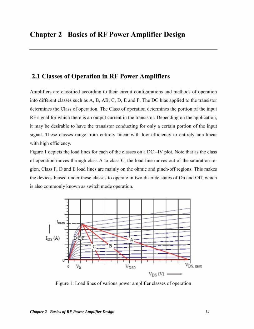
Chapter 2 Basics of RF Power Amplifier Design 14
Chapter 2 Basics of RF Power Amplifier Design
2.1 Classes of Operation in RF Power Amplifiers
Amplifiers are classified according to their circuit configurations and methods of operation
into different classes such as A, B, AB, C, D, E and F. The DC bias applied to the transistor
determines the Class of operation. The Class of operation determines the portion of the input
RF signal for which there is an output current in the transistor. Depending on the application,
it may be desirable to have the transistor conducting for only a certain portion of the input
signal. These classes range from entirely linear with low efficiency to entirely non-linear
with high efficiency.
Figure 1 depicts the load lines for each of the classes on a DC –IV plot. Note that as the class
of operation moves through class A to class C, the load line moves out of the saturation re-
gion. Class F, D and E load lines are mainly on the ohmic and pinch-off regions. This makes
the devices biased under these classes to operate in two discrete states of On and Off, which
is also commonly known as switch mode operation.
Figure 1: Load lines of various power amplifier classes of operation

Chapter 2 Basics of RF Power Amplifier Design 15
This chapter analyzes four classes (A, B, AB, and C) of power amplifier operation, which are
mainly associated with Doherty power amplifier operation. Figure 2 shows a summary of
these four power classes based on their transistor transfer characteristics and their classical
definitions.
(a)
(b)
Figure 2: (a), (b) Classes of operation of Power amplifiers and their standard definition [31]

Chapter 2 Basics of RF Power Amplifier Design 16
2.1.1 Class A
Class-A is the most linear of all amplifier class types. It can be defined, as an amplifier that is
biased such that the output current flows at all times and the input signal drive level is kept
small enough to avoid driving the transistor in to cut-off. In a Class A operation, the transis-
tor conducts for the full cycle of the input signal, meaning that the conduction angle of the
transistor is 360o. As seen in Figure 3, the bias point is set in the active region which is closer
to the center of the transistor’s range of operation.
Although class A amplifiers are highly linear, since the device is conducting at all times and
is constantly carrying current, consequently there is a continuous loss of power in the device,
which results in poor efficiency. The maximum efficiency of an ideal Class-A PA is 50 % at
peak envelope power. Due its linear nature, IMD and harmonic levels of a class A amplifier
decreases or increases monotonically with the input signal level. The low levels of harmonics
in the amplification process allows Class-A to be used at frequencies close to the maximum
capability (fmax) of the transistor. With good linearity but low efficiency, Class-A PAs are
suitable for applications requiring low power, high linearity, high gain and broadband opera-
tion.
Figure 3: Class A transfer characteristic [32]

Chapter 2 Basics of RF Power Amplifier Design 17
The DC power consumption of a class A amplifier can be calculated as:
dqdddc IVP ×= (2.1)
The maximum output power is:
dqddout_max IV
21P ××=
(2.2)
where Vdd= drain voltage and Idq= Quiescent current. Note that maximum ac output current
is equal to Idq.
2.1.2 Class B
This is an amplifier where the transistor conducts only half of the time either on positive or
negative half cycle of the input signal. The conduction angle for the transistor is approxi-
mately 180o. The class-B amplifier operates ideally at zero quiescent current. This is
achieved by biasing the transistor at its cut off voltage and any current through the device
goes directly to the load.
Compared to a class A amplifier the efficiency of a class B amplifier is higher. For an ideal
class B PA the maximum efficiency can reach up to 78.5 % at peak envelope power. Howev-
er, the trade-off is linearity. A typical Class-B amplifier will produce considerable amounts
of harmonic distortion that must be filtered from the amplified signal.
Class B power amplifiers are often implemented using push-pull configuration, which uses
two transistors in parallel [32]. In this configuration one transistor conducts during positive
half cycles of the input signal and the second transistor conducts during the negative half cy-
cle. This method ensures that the entire input signal is reproduced at the output. The DC
power consumption of a class B amplifier can be calculated as:
ac_maxdddc IV2P ××=
π (2.3)
where Vdd = drain voltage, Iac_max = maximum ac output current. Figure 4 shows how the
class-B amplifier operates.

Chapter 2 Basics of RF Power Amplifier Design 18
Figure 4: Class B transfer characteristic [32]
2.1.3 Class AB
In terms of linearity and efficiency, Class AB amplifiers are a balance between Class A and
Class B amplifiers. The dc operating point of the class AB operation is in the region between
the cut-off point and the Class A bias point. This would lead to a quiescent current of 10% -
15% percent of Idss. The conduction angle in Class-AB is between 180o and 360 o which
would have the transistor on for more than half a cycle, but less than a full cycle of the input
signal. The linearity of a class AB power amplifier is closer to Class A operation and its max-
imum efficiency is between 50% -78.5%.
2.1.4 Class C
In class C operation the conduction angle for the transistor is significantly less than 180o. It is
biased so that the output current is zero for more than one half cycle of the input signal. Lin-
earity of the Class-C amplifier is the poorest of the four classes of amplifiers discussed in this
chapter. The maximum Efficiency of Class-C can approach as high as 85 %.

Chapter 2 Basics of RF Power Amplifier Design 19
Figure 5: Class AB transfer characteristic [32]
2.1.5 Additional power Classes
There are additional power classes such as F, D, E, G, H, and S. All these classes are catered
for power amplifiers that target high-efficiency performance. Each of these classes uses a va-
riety of techniques to reduce the average drain power to achieve high efficiency. For in-
stance, Class F uses harmonic resonators in the output network to shape the drain waveforms
to achieve high efficiency. Classes D, E, and S use switching techniques. Classes G and H
use resonators and multiple power-supply voltages to reduce the drain current-voltage prod-
uct.
Classes S, D, E, F, G, and H are widely used for narrowband tuned amplifiers that require
higher efficiency but do not require linear amplification, such as amplification of CW, FM or
PM that have constant envelopes.
2.2 Power Amplifier Performance Metrics
Power amplifiers are available in various form factors ranging from miniature ICs to high
power transistors on printed circuit boards. Depending on the various system requirements,

Chapter 2 Basics of RF Power Amplifier Design 20
the specific requirements of a given power amplifier will also vary considerably. However,
there are common metrics, such as linearity, efficiency, gain flatness, noise figure and stabil-
ity that are used to assess the performance of any type of PA. Often design trade-offs are re-
quired to optimize one parameter over another and necessitates performance compromises.
In this section, a few common amplifier performance metrics are discussed.
2.2.1 Stability
Stability refers to an amplifier's resistance to causing spurious oscillations. Means of feed-
back and gain are the fundamental conditions for oscillation. Ensuring stability of an amplifi-
er with considerable gain over a large bandwidth would require that all conducted and radiat-
ed feedback paths are sufficiently attenuated. A conducted feedback path could be through a
bias feedback and a radiated feedback path could be in the form of a waveguide cavity in
which active elements are shielded with.
Although it is expected for an amplifier to be stable, often it is difficult to determine if this is
the case in RF power amplifier applications. For instance, while it may appear that there are
no obvious oscillations generated from the amplifier, it can be such that the oscillation fre-
quency is low enough that the DC blocking capacitors attenuate the signal sufficiently to
make it very difficult to measure. Or there may appear an unexplained spurious signal at high
frequencies in the output spectrum that is the mixing product of the desired signal and an os-
cillation tone that is out of band of the measuring receiver.
A formal set of conditions for unconditional stability can be expressed in a set of formulas by
the Rollett's stability factor (K factor):
(2.4)
along with one of the following auxiliary conditions: B1 = 1 + |S11|2 − |S22|2 − |∆|2 > 0
B2 = 1 + |S22|2 − |S11|2 − |∆|2 > 0
β1 = 1 − |S22|2 − |S12S21| > 0
Chapter 2 Basics of RF Power Amplifier Design 21
β2 = 1 − |S11|2 − |S12S21| >0
The above conditions only apply when source and load reflection coefficients have a magni-
tude of less than one (Γin< 1 and Γout < 1).
2.2.2 1 dB Compression point (P1dB) and Psat
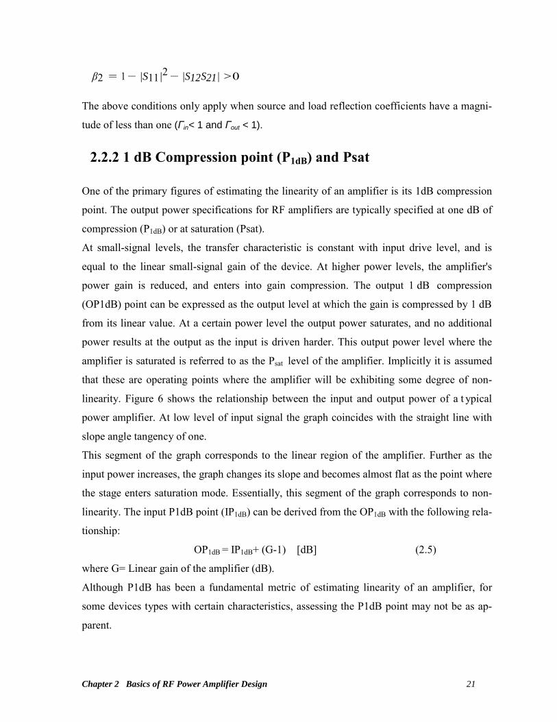
One of the primary figures of estimating the linearity of an amplifier is its 1dB compression
point. The output power specifications for RF amplifiers are typically specified at one dB of
compression (P1dB) or at saturation (Psat).
At small-signal levels, the transfer characteristic is constant with input drive level, and is
equal to the linear small-signal gain of the device. At higher power levels, the amplifier's
power gain is reduced, and enters into gain compression. The output 1 dB compression
(OP1dB) point can be expressed as the output level at which the gain is compressed by 1 dB
from its linear value. At a certain power level the output power saturates, and no additional
power results at the output as the input is driven harder. This output power level where the
amplifier is saturated is referred to as the Psat level of the amplifier. Implicitly it is assumed
that these are operating points where the amplifier will be exhibiting some degree of non-
linearity. Figure 6 shows the relationship between the input and output power of a t ypical
power amplifier. At low level of input signal the graph coincides with the straight line with
slope angle tangency of one.
This segment of the graph corresponds to the linear region of the amplifier. Further as the
input power increases, the graph changes its slope and becomes almost flat as the point where
the stage enters saturation mode. Essentially, this segment of the graph corresponds to non-
linearity. The input P1dB point (IP1dB) can be derived from the OP1dB with the following rela-
tionship:
OP1dB = IP1dB+ (G-1) [dB] (2.5)
where G= Linear gain of the amplifier (dB).
Although P1dB has been a fundamental metric of estimating linearity of an amplifier, for
some devices types with certain characteristics, assessing the P1dB point may not be as ap-
parent.

Chapter 2 Basics of RF Power Amplifier Design 22
For instance, due to the smooth transition from the linear to the saturation region, GaN am-
plifiers typically define their output power at the 3dB compression point.
Figure 6: 1 dB Compression point (P1dB) and Psat
2.2.3 Efficiency
Efficiency is a measure of a device’s ability to convert one energy source to another. In pow-
er amplifier design, efficiency indicates the Power Amplifier’s ability to convert the DC
power of the supply into the signal power delivered to the load. Power that is not converted
to useful signal is dissipated as heat. Therefore Power Amplifiers that has low efficiency
have high levels of heat dissipation. To obtain the maximum efficiency of a RF power ampli-
fier, one has to consider multiple aspects of the design as frequency, temperature, input drive
level, load impedance, bias point, device geometry, and intrinsic device characteristics. In
typical microwave designs, efficiency is presented in three forms:
• Drain efficiency: Drain efficiency is the ratio of output RF power to input DC power.
DCDC
RFout
DC
RFout
IVP
P P
×==η (2.9)
In this unit of measure the incident input RF power that goes into the device is disregarded.
• Power added efficiency (PAE): Power added efficiency takes into account the input RF
power to the device in its calculation of efficiency.

Chapter 2 Basics of RF Power Amplifier Design 23
DCDC
RFinRFout
DC
RFinRFout
IVP -P
PP - P
×==PAE (2.10)
A theoretical amplifier with infinite linear gain will have the same efficiency value with the
drain efficiency and PAE calculations. In practical amplifiers PAE will always be less than
drain efficiency. Although for amplifiers with high gain the two calculations would yield
very close results, since the input power levels are only a fraction of the output power.
• Total efficiency: Total efficiency gives a complete sense of the ratio of output power to
both types of DC and RF input power.
RFinDCDC
RFout
RFinDC
RFouttotal
P )I(VP
PP P
+×==
+P (2.11)
2.2.4 Linearity
All RF microwave circuits generate signal distortion as a result of non-linear behavior .In a
RF power amplifier, it is inevitable that non-linear behavior exists which is attributed mainly
to gain compression. It is characterized by various techniques depending upon s pecific
modulation and application. Harmonics, Inter-modulation distortion and intercept points are
few of the most commonly used figures for quantifying linearity.
• Intermodulation distortion (IMD): When multiple signals are injected to an amplifier
simultaneously, the sum and difference products of each of the fundamental input signals
and their associated harmonics create distortion products, which are referred to as inter-
modulation distortion (IMD). IMD products are more difficult to deal with compared to
harmonic distortion. Harmonics can be filtered from the output spectrum but IMD prod-
ucts, especially third order IMD products occur close to the desired signal.
Also lower frequency second-order IMD products can interfere with the DC bias of the tran-
sistor, increasing the non-linearity and decreasing efficiency. When two signals at frequen-
cies f1 and f2 are input to any nonlinear amplifier, the following output components will re-
sult as in Figure 7.
Note that odd order intermodulation products (2f1-f2, 2f2-f1, 3f1-2f2, 3f2-2f1) are close to
the two fundamental tone frequencies f1 and f2.

Chapter 2 Basics of RF Power Amplifier Design 24
The magnitude of Intermodulation distortion can be given by:
IMD (dBc) = Pout1dB – PoutIMD (2.12)
Figure 7: Frequency spectrum of a two-tone signal
where PoutIMD represents the output power of the third order intermodulation product. IMD
magnitudes can increase with carrier spacing and can distort the output signal significantly as
wider bandwidths are explored. Therefore, it is important to minimize IMD products as much
as possible when designing RF amplifiers for wide bandwidths.
• Intercept point: As the input power to a power amplifier is increased, the slope of the
amplitude of the harmonics at the output increases more swiftly with respect to the fun-
damental tone. If the amplitude of the fundamental and higher order products are plotted
on a log scale with their respective slopes, the intercept point is where their linear exten-
sion intersects with the linear extension of the 1:1 slope of the fundamental slope. Figure
8 represents the second and third order intercept points (IP2 and IP3) in a plot of input
power versus the output power. Third order intercept point (IP3) in particular plays a
significant role in assessing a power amplifiers performance. Higher the IP3, lower is the
distortion at higher power levels. The magnitude of the third order output intercept
(OIP3) point and the third order input intercept point (IIP3) can be calculated as follows:
2
3 , IMDoutout
PPOIP += (2.13)
GainOIPIIP −= 33 (2.14)

Chapter 2 Basics of RF Power Amplifier Design 25
Figure 8: Second and third-order intercept points
2.3 Efficiency Enhancement Techniques
With wireless communication systems evolving, standards such as LTE use more efficient
modulation schemes as orthogonal frequency division multiple access (OFDMA) to achieve
higher data rates and better spectral efficiency. The non-constant envelope signals of these
systems have large peak-to-average power ratios (PAPRs) of around 6-10dB [33]. The RF
power amplifier (PA) that amplifies the output signals of these systems faces challenges to
achieve increased bandwidth, to minimize the size, to achieve high efficiency while main-
taining linearity.
Power amplification of amplitude-modulated signals with fluctuating envelopes used in these
systems face challenges where the modulated signal gets distorted when the power amplifier
is used at its full rated RF power level. An apparent solution is to operate the power amplifier
in the linear region where the average output power is much smaller than the amplifier’s sat-
uration power. But this increases cost and reduces efficiency, since the most efficient opera-
tion of a power amplifier is near compression. In addition to non-linearity, power amplifiers
also possess memory effects that contribute to the distortion of the input signal when the sig-
nal has a broad envelope or video bandwidth. Memory effect could be explained as a time lag
between AM-AM (amplitude dependent gain) and AM-PM (amplitude dependent phase
shift) response of the amplifier by changes in the modulation frequency [16]. The most
Chapter 2 Basics of RF Power Amplifier Design 26
common outcome of memory effects in an amplifier is the variation of IMD3 sidebands with
tone spacing and asymmetry between the lower and upper band IMD3 [16, 34].One approach
to reduce nonlinear distortion is the linearization of the power amplifier. Several linearization
techniques such as Feed Forward Linearization [8-9], Cartesian Feedback [10-11], LINC
(Linear amplification using Nonlinear components) [12] and Digital pre distortion (DPD)
[13-15] have been developed. Note that one of the main consequences of memory effect is
that it makes most standard linearization in efficient [16]. Even though there are a number of
Digital pre distortion (DPD) algorithms that do correct for some memory effects [13], it is
fundamentally important to minimize the memory effects at the amplifier design level. Alt-
hough these linearization techniques fulfill the linearity requirements, it ma y contribute to
overall efficiency degradation due to additional circuitry involved in the linearization pro-
cess.
Another challenge is to achieve high efficiency at two power levels for non-constant enve-
lope signal amplification. Maximum efficiency is attained only at one single power level,
usually closer to the maximum rated power of the device. For a signal with a 6-10dB PAPR,
efficiency would be degraded in the back-off power level. An implementation of efficiency
enhancement technique that results in high efficiency in the back-off power level of opera-
tion of the power amplifier would be the solution for this issue. Several efficiency enhance-
ment techniques have such as Chireix Outphasing [22 - 24], Envelope elimination and resto-
ration (EER) [25-27], Doherty [28] and Envelope tracking (ET) [29] have been suggested
and studied to date.
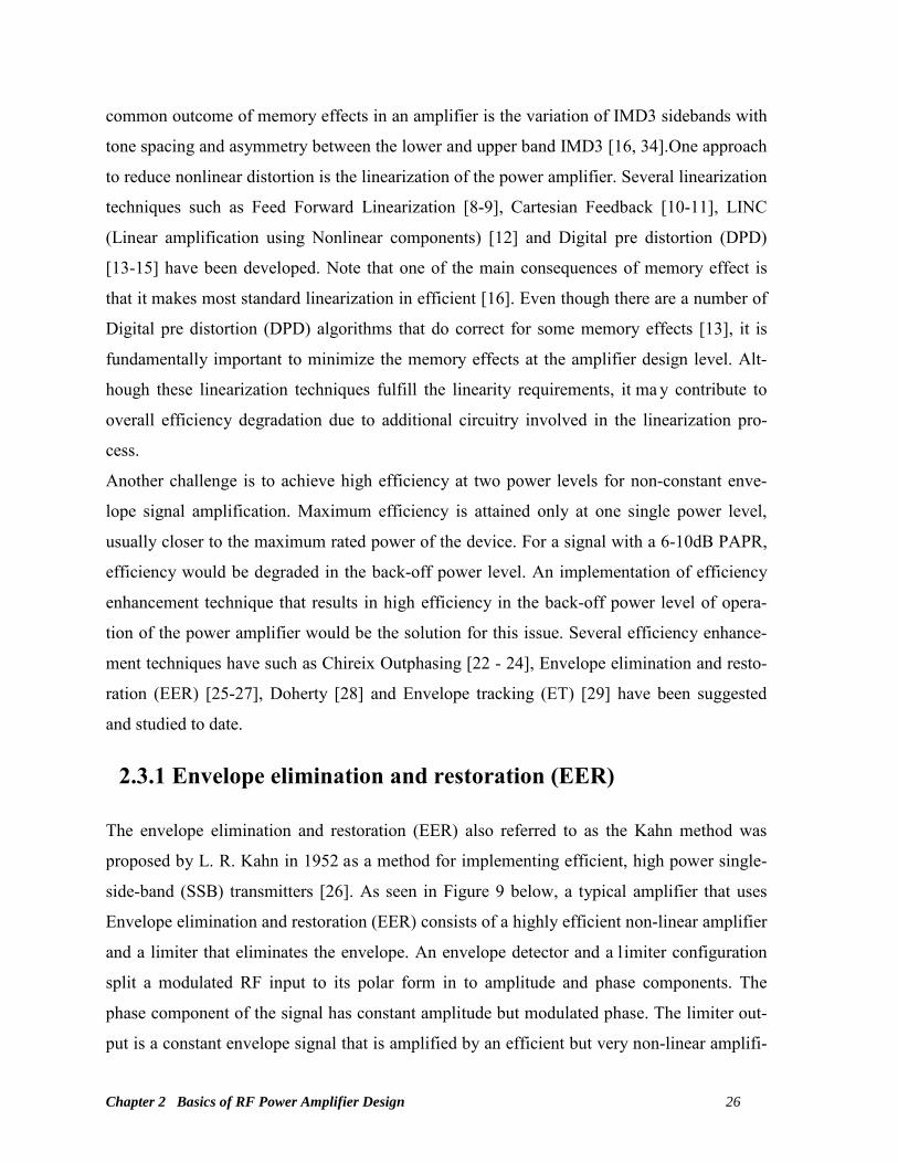
2.3.1 Envelope elimination and restoration (EER)
The envelope elimination and restoration (EER) also referred to as the Kahn method was
proposed by L. R. Kahn in 1952 as a method for implementing efficient, high power single-
side-band (SSB) transmitters [26]. As seen in Figure 9 below, a typical amplifier that uses
Envelope elimination and restoration (EER) consists of a highly efficient non-linear amplifier
and a limiter that eliminates the envelope. An envelope detector and a limiter configuration
split a modulated RF input to its polar form in to amplitude and phase components. The
phase component of the signal has constant amplitude but modulated phase. The limiter out-
put is a constant envelope signal that is amplified by an efficient but very non-linear amplifi-

Chapter 2 Basics of RF Power Amplifier Design 27
er. A constant envelope enables the non-linear amplifier to operate near compression without
any distortion, enhancing its efficiency. The envelope information is restored at the output by
modulating the supply voltage (Vdd) of the amplifier, where the modulating signal is derived
from the envelope detector.
There are various issues that need to be resolved when implementing this method. There
could be phase and gain mismatch between the RF and envelope paths due to different cir-
cuits that are operated at different frequencies. Correcting for this type of mismatch could be
complex. The dc controller’s efficiency and bandwidth would add further limitations as well.
The association between the PA and drain modulator is a complex and costly implementation
as well.
Figure 9: Envelope elimination and restoration (EER) system block diagram [35]
2.3.2 Envelope tracking (ET)
Envelope tracking is a method similar to the EER technique; however the limiter circuit is
not required as shown in Figure 10. It superimposes the envelope signal at the drain by dy-
namically varying supply voltage that conserves power while allowing the PA to operate in
linear mode. The difference between this technique and EER is the input signal that contains
both amplitude and phase information. It maximizes PA efficiency by keeping RF transistor
closer to saturation for all envelope amplitudes. Though the performance of envelope track-

Chapter 2 Basics of RF Power Amplifier Design 28
ing is better than a linear amplifier, it is not as good as the EER technique. This is due to the
increased flexibility of the supply voltage control, compared to the EER technique. On an ET
system the drain modulator does not have to perfectly match with the input envelope which
allows more errors and design relaxation, compared to EER.
The design of a highly efficient dc modulator with high output voltage and current is the big-
gest challenge of implementing this technique. Although ET yields lower efficiency com-
pared to EER, it is more attractive and has already been implemented in several RF applica-
tions today [29, 36] because of its simplicity and practicality compared to EER.
Figure 10: Envelope Tracking (ET) system block diagram
2.3.3 Chireix Outphasing
Chireix outphasing power amplifier system was first introduced by Henri Chireix in 1930s
[22]. Chireix Power combining system uses two nonlinear amplifiers to amplify two input
signals with different phases, which are finally combined at the output to regain amplitude
and phase modulated signal. Firstly, a single input signal containing both amplitude and
phase modulation is divided into two constant envelope input signals by an AM-PM modula-
tor where the input signal amplitude is transformed into phase deviation [17]. Conventional
power combining at the output could result in severe losses when the phases of the two signal
paths vary. A Chireix combiner has resolved this issue by a reactance compensation load de-
sign technique that further results in improved efficiency in the back-off region. At two pre-

Chapter 2 Basics of RF Power Amplifier Design 29
defined phase offset values, the generator sees a purely resistive load impedance resulting in
maximum power combining efficiency. Thorough explanation of the principle and in depth
details of the load design and other practical issues are available in [17, 37, 38].
2.3.4 Doherty Amplification Technique
William H. Doherty first introduced the Doherty technique in 1936 [28] which was originally
designed using vacuum tubes. This is one of the most implemented techniques today for im-
proving efficiency at back-off output power levels. Doherty technique involves the imple-
mentation of efficiency enhancement on a power amplifier circuit that requires linear ampli-
fication. Linear amplification is required when the signal contains AM (Amplitude Modula-
tion) or a combination of both, Amplitude and Phase Modulation (SSB, QPSK, QAM,
OFDM).
The most conventional configuration of a Doherty circuit is shown in Figure 11. It consists of
two amplifiers, namely the main and the peaking. The peaking amplifier is also known as the
“auxiliary” amplifier. The amplifiers are connected in parallel with their outputs joined by a
quarter-wave transmission line, which performs impedance transformation.
Figure 11: Doherty amplifier block diagram

Chapter 2 Basics of RF Power Amplifier Design 30
Each amplifier is biased into different bias conditions. The main amplifier is typically biased
in Class AB and the peaking amplifier in class C. It is designed to have different load termi-
nations at multiple power levels, so it has the optimized performed for each power level. The
conventional Doherty amplifier design uses two amplifiers to compromise between efficien-
cy and linearity in low power and high power regions.
The peaking amplifier is used to control the load of the main amplifier for a particular range
of input power level. The main amplifier is designed such that it w ill saturate at a certain
backed off power level from the power amplifiers nominal output power level. This is per-
formed by presenting a higher impedance at that particular backed off power level. Note that
only the main amplifier operates at this backed off power level. As the main amplifier satu-
rates, the peaking amplifier starts to deliver current, reducing the impedance seen at the out-
put of the main amplifier. For instance, for a conventional symmetrical Doherty operation
where the main and peaking amplifiers have the same device sizing, at a 6dB backed off
power level the main amplifier would be presented with two times its optimum impedance.
When the main amplifier saturates, the peaking amplifier will start to operate and modulate
the main amplifier load from twice the optimum impedance to its optimum impedance. The
peaking amplifier is turned on only during the peaks of the input signal. This is achieved by
biasing the device in class C where the bias point is below its pinch-off voltage. Consequent-
ly, the peaking amplifier gets turned on when the main amplifier reaches a level closer to sat-
uration. Since the main amplifier remains closer to saturation for a range of 6 dB backed off
from the maximum input power, the total efficiency of the system remains high over the full
dynamic range.
The Design principles of the conventional Doherty amplifier will be further discussed in de-
tail in section 2.5. In order to optimize the Doherty PA architecture for various signal condi-
tions, the standard Doherty Architecture can be further branched out to various sub catego-
ries. There can be several variations of the standard Doherty amplifier architecture. The ma-
jority of these variations can be subdivided into three basic categories: symmetrical, asym-
metrical, and N-stage Doherty.
• Symmetrical Doherty architecture: This is the most conventional and commonly used
Doherty amplifier architecture, which was discussed in section 2.3.4. The main benefit of
using this architecture is its simplicity. Since the main and peaking amplifiers use the

Chapter 2 Basics of RF Power Amplifier Design 31
same device sizing (same peak power capability), the same matching networks can be uti-
lized with a relatively simple 3 dB power splitting at the input, usually implemented with
a 90 degree hybrid. The downside of this architecture is that its only optimum for signals
with a 6dB peak to average ratio (PAR). This is due to the fact that the second efficiency
peak of a symmetrical Doherty design falls at an output power range that is 6dB backed
off from its peak power. Therefore for a signal with a higher than 6dB peak to average ra-
tio (PAR), the full efficiency benefit introduced by a symmetrical Doherty would not be
properly utilized. Figure 12 shows an efficiency plot of a symmetrical Doherty PA com-
pared to a class B PA.
• Asymmetrical Doherty Architecture: The main difference of an asymmetrical Doherty in
comparison with a symmetrical Doherty is the use of devices with different peak power
capabilities for main and peaking amplifiers. The power ratio between the peak and main
amplifier is dependent on the design requirement of where the second efficiency peak
needs to be at.
Figure 12: Efficiency of a conventional symmetrical Doherty PA compared to a class B PA
[82].

Chapter 2 Basics of RF Power Amplifier Design 32
The advantage of the asymmetric Doherty architecture is that the main-peak power ratio can
be selected such that the optimum back off efficiency point can be achieved for signals with
PARs in the range of 6-10dB, whereas with a symmetrical Doherty architecture the optimum
back off efficiency is limited to only 6dB. The theory and implementation of asymmetric
Doherty architecture is well described in [39].
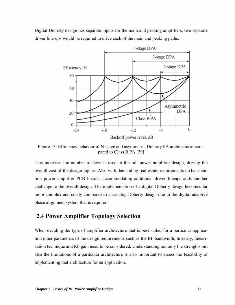
• N-stage Doherty Architecture: The N-stage Doherty implies the use of “N” number of
peaking amplifiers (biased in class C or B) rather than a single peaking amplifier as in
the asymmetrical/symmetrical amplifier architecture. At higher drive levels, all of the
peaking amplifiers will be engaged and will be contributing to the overall output-
combined signal level. At low drive levels only the main amplifier would be turned on.
The output power versus efficiency curve of a N-stage Doherty design would consist of
N number of efficiency peaks, offering the capability of presenting a high efficiency
response at multiple back off power levels. Theory and implementation of N Doherty
architecture is well described in [40, 41]. Figure 13 summarizes the efficiency behav-
iour of the above described Doherty architectures.
• Digital Doherty: Although the concept of Doherty architecture has been around for
several years, the various enhancements and extensions of this architecture have mostly
been based on the standard analog Doherty. The concept of digital Doherty was intro-
duced and explored more in recent years. The basic architecture of a d igital Doherty
consists of separate dual-inputs for the main and peaking amplifiers that is digitally
driven. By using digital adaptive phase alignment techniques the performance degrada-
tion that is caused by the bias and power dependent phase misalignment between the
main and peaking branches is compensated.
Although research has demonstrated, that in comparison with the conventional analog
Doherty PA, a digital Doherty PA can achieve a 10% improvement in PAE over the same
back off output power range [42], there are some drawbacks of implementing digital
Doherty. For an analog Doherty design, a single input signal is split to drive the main and
peaking amplifiers. Therefore, only a single line-up of driver amplifiers is required. Since a
Chapter 2 Basics of RF Power Amplifier Design 33
Digital Doherty design has separate inputs for the main and peaking amplifiers, two separate
driver line-ups would be required to drive each of the main and peaking paths.
Figure 13: Efficiency behavior of N-stage and asymmetric Doherty PA architectures com-
pared to Class B PA [39]
This increases the number of devices used in the full power amplifier design, driving the
overall cost of the design higher. Also with demanding real estate requirements on base sta-
tion power amplifier PCB boards, accommodating additional driver lineups adds another
challenge to the overall design. The implementation of a digital Doherty design becomes far
more complex and costly compared to an analog Doherty design due to the digital adaptive
phase alignment system that is required.
2.4 Power Amplifier Topology Selection
When deciding the type of amplifier architecture that is best suited for a particular applica-
tion other parameters of the design requirements such as the RF bandwidth, linearity, lineari-
zation technique and RF gain need to be considered. Understanding not only the strengths but
also the limitations of a particular architecture is also important to assess the feasibility of
implementing that architecture for an application.

Chapter 2 Basics of RF Power Amplifier Design 34
Figure 14 represents the theoretical efficiency plots of some of the efficiency enhancement
techniques discussed above. Doherty being a well understood and mature technique has
many advantages over other efficiency enhancement techniques. Although efficiency enhanc-
ing techniques like Envelope Elimination and Restoration and Envelope tracking may pro-
vide greater performance than Doherty, their corresponding architectures are far more com-
plex, costly to implement and as discussed previously, have various issues involved in im-
plementation. The Doherty PA can accomplish high efficiency without adding any extra cir-
cuitry such as complex envelope control circuits used in Envelope elimination and restoration
and Envelope tracking .Due to the simplicity of the Doherty configuration, conventional lin-
earization methods like feed-forward and digital pr e-distortion can be easily implemented
with the Doherty amplifier. Compared to EER, ET and Chierex out phasing, Doherty tech-
nique also has much larger video bandwidth [41] which also helps to minimize memory ef-
fects. The main limiting factor of the Doherty technique is the quarter wave transformer. This
makes this method limited to only narrow band designs. Since modern wireless communica-
tion spectrums utilize narrow bandwidths, this is not a severe drawback.
Another shortcoming is the gain degradation caused due to the peaking amplifier. The typical
degradation for a s ymmetric Doherty design is around 2dB. As long as this degradation is
considered at an early design stage in the link budget, appropriate driver amplifiers can be
selected to compensate for this. This degradation can be also kept low with a higher gain
main amplifier at low power levels. Another familiar issue that can be seen from the configu-
ration of a Doherty system is resistive load matching. Techniques such as using offset lines to
load modulate reactive termination have been studied [41] and been implemented in designs.
Achieving high efficiency for a p ico-cell base station power amplifier would be tackled in
this thesis. One of the main challenges of a pico-cell base station is the limited real estate.
Since a Doherty PA can accomplish high efficiency at back- off power levels without adding
any extra circuitry, this technique can be implemented on an integrated circuit (IC).Which
makes this technique an ideal candidate for a pico cell application. Since the peak to average
ratio of the signal of the targeted 4G standard would be around 6dB, a symmetrical Doherty
design was selected for this design.

Chapter 2 Basics of RF Power Amplifier Design 35
Figure 14: Theoretical efficiency behavior of various efficiency enhancement techniques [83].
2.5 Doherty Operation
The fundamental principle of operation of the Doherty architecture was briefly discussed in
section 2.3.4. In this section an in-depth analysis of its operating principle is presented.
2.5.1 Doherty load modulation technique
As discussed in section 2.3, the most conventional configuration of a Doherty circuit consists
of two amplifiers, namely the main and the peaking amplifiers. The peaking amplifier is also
known as the “auxiliary” amplifier. The amplifiers are connected in parallel with their out-
puts joined by an impedance inverting quarter-wave transmission line. Each amplifier is bi-
ased into different bias conditions. The main amplifier is typically biased in Class AB and the
peaking amplifier in class C. It is designed to have different load terminations at multiple
power levels, so it has the optimized performed for each power level. Although the final out-
put power is the combined output power of both main and peaking amplifiers, as the input
drive level is reduced to a level typically 6dB below the maximum output power, the peaking
amplifier is turned off. Therefore below the 6dB back off position, the number of active de-
vices has been reduced by half, improving the efficiency at lower power levels significantly.

Chapter 2 Basics of RF Power Amplifier Design 36
One of the key elements of the Doherty architecture is the active pulling or modulation of the
main amplifier load impedance by the activity of the peaking amplifier. The active load pull
technique is based on the principle that applying current from a second source can vary the
resistance or reactance of a RF load. This concept is presented by Cripps in [17] as follows:
Figure 15: Active load modulation technique
Basic circuit theory suggests that when the supply current I2 of generator 2 i s set to zero,
generator 1 would see a load resistance of RL. If generator 2 starts to supply current along
with generator 1 (I1 and I2 > 0), the voltage appearing across the load resistor RL would
change along with the resistance seen by generator 1 and generator 2.This concept can be ex-
tended to ac circuits by using complex notation for representing the magnitude and the phase
of the currents and voltages and the resistive and reactive components.
Therefore the impedance seen by generator 1 and generator 2 when both generators are sup-
plying current can be represented as:
+=
1
21 1
IIRZ L (4.1)
+=
2
12 1
IIRZ L (4.2)
If I2 is in phase with I1, the impedance Z1 seen by generator 1 can be transformed to higher
value. If I2 is out of phase with I1, Z1 can be transformed to a smaller value. A key point to
illustrate in the Doherty operation is the impedance inversion performed by the λ/4 wave
transformer. A few derivations according to [17] are presented in order to illustrate the rela-
tionship between the voltages, currents and the impedances of the main and peaking amplifi-
ers. Figure 16 shows an operational diagram to analyze the Doherty amplifier circuit.
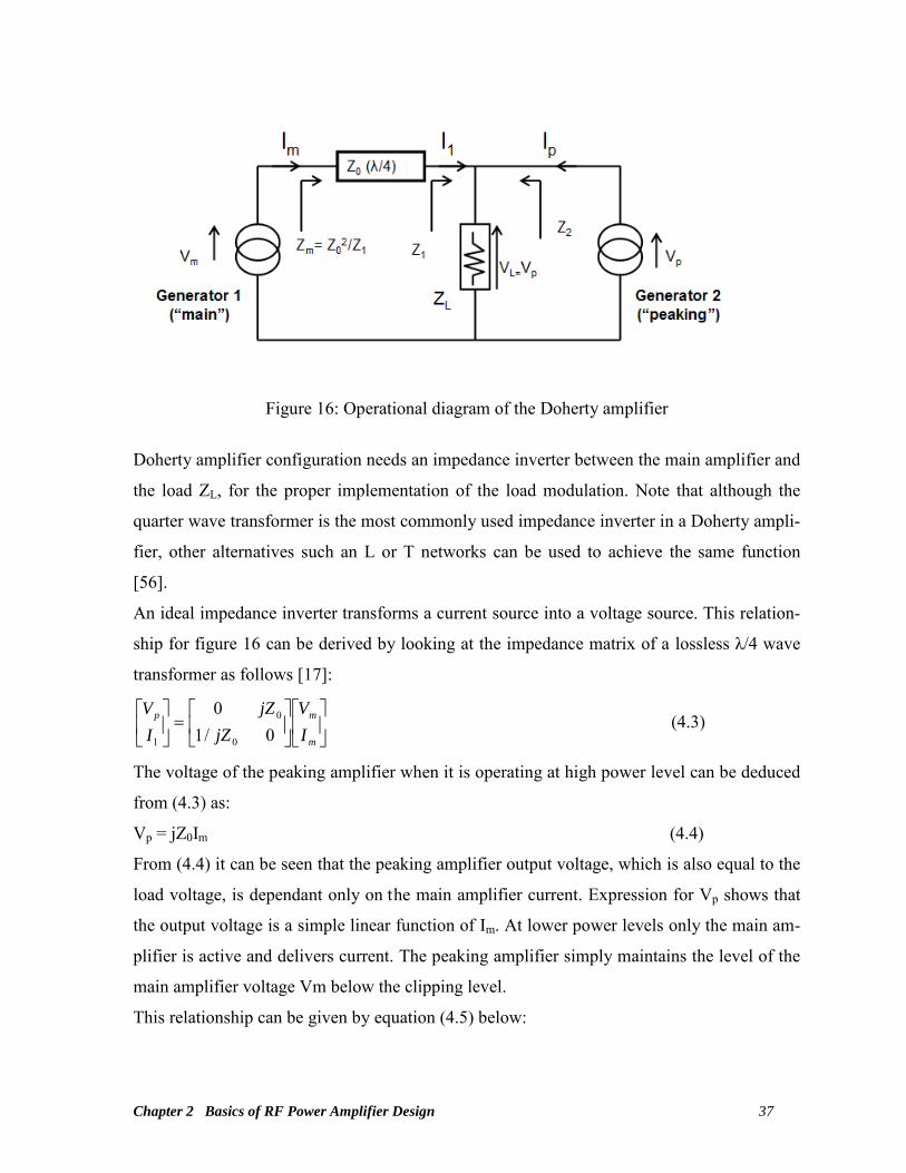
Chapter 2 Basics of RF Power Amplifier Design 37
Figure 16: Operational diagram of the Doherty amplifier
Doherty amplifier configuration needs an impedance inverter between the main amplifier and
the load ZL, for the proper implementation of the load modulation. Note that although the
quarter wave transformer is the most commonly used impedance inverter in a Doherty ampli-
fier, other alternatives such an L or T networks can be used to achieve the same function
[56].
An ideal impedance inverter transforms a current source into a voltage source. This relation-
ship for figure 16 can be derived by looking at the impedance matrix of a lossless λ/4 wave
transformer as follows [17]:
=
m
mp
IV
jZjZ
IV
0/10
0
0
1
(4.3)
The voltage of the peaking amplifier when it is operating at high power level can be deduced
from (4.3) as:
Vp = jZ0Im (4.4)
From (4.4) it can be seen that the peaking amplifier output voltage, which is also equal to the
load voltage, is dependant only on the main amplifier current. Expression for Vp shows that
the output voltage is a simple linear function of Im. At lower power levels only the main am-
plifier is active and delivers current. The peaking amplifier simply maintains the level of the
main amplifier voltage Vm below the clipping level.
This relationship can be given by equation (4.5) below:
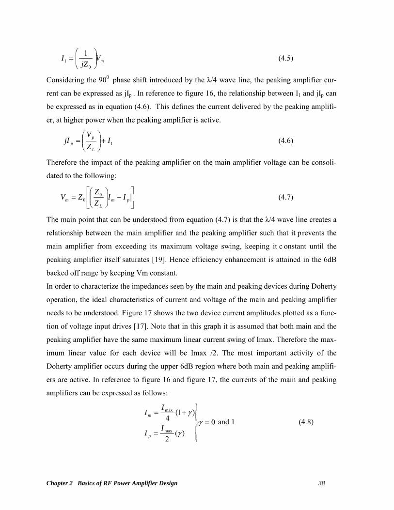
Chapter 2 Basics of RF Power Amplifier Design 38
mVjZ
I
=
01
1 (4.5)
Considering the 900 phase shift introduced by the λ/4 wave line, the peaking amplifier cur-
rent can be expressed as jIp . In reference to figure 16, the relationship between I1 and jIp can
be expressed as in equation (4.6). This defines the current delivered by the peaking amplifi-
er, at higher power when the peaking amplifier is active.
1IZV
jIL
pp +
= (4.6)
Therefore the impact of the peaking amplifier on the main amplifier voltage can be consoli-
dated to the following:
−
= pm
Lm II
ZZ
ZV 00 (4.7)
The main point that can be understood from equation (4.7) is that the λ/4 wave line creates a
relationship between the main amplifier and the peaking amplifier such that it prevents the
main amplifier from exceeding its maximum voltage swing, keeping it c onstant until the
peaking amplifier itself saturates [19]. Hence efficiency enhancement is attained in the 6dB
backed off range by keeping Vm constant.
In order to characterize the impedances seen by the main and peaking devices during Doherty
operation, the ideal characteristics of current and voltage of the main and peaking amplifier
needs to be understood. Figure 17 shows the two device current amplitudes plotted as a func-
tion of voltage input drives [17]. Note that in this graph it is assumed that both main and the
peaking amplifier have the same maximum linear current swing of Imax. Therefore the max-
imum linear value for each device will be Imax /2. The most important activity of the
Doherty amplifier occurs during the upper 6dB region where both main and peaking amplifi-
ers are active. In reference to figure 16 and figure 17, the currents of the main and peaking
amplifiers can be expressed as follows:
0)(
2
)1(4
max
max
=
=
+=γ
γ
γ
II
II
p
m
and 1 (4.8)

Chapter 2 Basics of RF Power Amplifier Design 39
Figure 17: Main and peaking device currents Vs input voltage amplitude where γ = 0 corresponds to the 6dB back off point and γ = 1 to the maximum power point.
Now we can proceed to derive how the λ/4 wave transformer, causes the impedance seen by
the main amplifier to reduce as the peaking amplifier current Ip increases. If the load modula-
tion equation (4.1) and (4.2) is applied to Figure 16, the impedances on each side of the load
impedance ZL can be gives as:
+=
11 1
II
ZZ pL (4.9)
+=
pL I
IZZ 12 1 (4.10)
The relationships between the input and output voltages and currents of the λ/4 wave
transformer can be defined as follows:
I1Vp = ImVm (4.11)
since
12
0 ZZZ m= (4.12)

Chapter 2 Basics of RF Power Amplifier Design 40
and
=
1
20 I
VIV
Z p
m
m (4.13)
From (4.13) and (4.11):
0
1 ZV
I m= (4.14)
Substituting I1 in the expression for Z1 in (4.9) would give:
+=
m
pL V
ZIZZ 0
1 1 (4.15)
Substituting (4.15) in (4.12) gives the output impedance seen by the main device:
+
=
m
pL
m
VZI
Z
ZZ
0
20
1 (4.16)
where Vm = ImZm. By using the relationship defined in (4.8) and (4.16), Vm (which is the am-
plitude of the RF voltage swing at the output of the main device) can be re-written as the fol-
lowing:
+
+
=
mL
m
V
ZI
Z
IZ
V
0max
max20
)(21
)1(4
γ
γ (4.17)
(4.17) can be re-written as:
( ))2(22 00max0
LL
m ZZZI
ZZ
V −+
= γ (4.18)
Earlier it was stated that the λ/4 wave line creates a relationship between the main amplifier
and the peaking amplifier such that it prevents the main amplifier from exceeding its maxi-
mum voltage swing, keeping it constant until the peaking amplifier itself saturates. Therefore
efficiency enhancement in the 6dB backed off range is attained when Vm remained constant.

Chapter 2 Basics of RF Power Amplifier Design 41
By examining equation (4.18) it can be seen that the main device voltage becomes independ-
ent of γ and Vm remains constant only if Z0 = 2ZL .Therefore, by having the characteristic
impedance of the λ/4 wave line twice the resistive load, the main amplifier sees twice the
output impedance and reaches the maximum voltage when the current is only half the maxi-
mum value at back off power levels.
2.5.2 Doherty Amplifier Operation
The Doherty amplifier operation can be described based on three operating regions related to
the input power levels, namely low, medium and high power regions. Depending on the input
drive level, the load impedances seen by the main and peaking amplifier will change based
on the technique described in section 2.5.1.
Based on figure 16, the load impedances of main and peaking amplifiers for the operating
regions can be summarized as follows by equation (4.19) and (4.20) [17]:
+
=
m
pmL
L
m
III
Z
Z
ZZ
Z2
0
20
maxmax
max
2
20
ininin
inin
VVV
VV
<<
<<
(4.19)
+
∞=
p
pmL I
IIZ
Z 2
maxmax
max
2
20
ininin
inin
VVV
VV
<<
<<
(4.20)

Chapter 2 Basics of RF Power Amplifier Design 42
• Low power region of operation:
In the low-power region (2
0 maxinin
VV << ), the peaking amplifier is turned off and in refer-
ence to figure 18, the main amplifier sees the load Z1 inverted to Zm by the λ/4 line. The
peaking amplifier sees very large impedance (theoretically an open circuit) and facilitates the
load impedance of the main amplifier to be two times larger than that of the optimum re-
sistance required to deliver maximum power. Therefore, the high output impedance seen by
the main amplifier forces it to saturate prematurely. At this point, at an input voltage
of2maxinV , the maximum fundamental current swing is half and the voltage swing reaches Vdc
which is the ideal maximum voltage swing [17]. As a consequence of this, half of the main
amplifier’s allowable power level (a quarter of the total maximum power or 6 dB down from
the total maximum power) is presented, while the efficiency is equal to the maximum effi-
ciency of the main amplifier. This is shown in figure 19 below. Note that, 78.5% theoretical
maximum efficiency illustrated in figure 19 is based on a class B operation of the main am-
plifier. In conclusion, at low input drive levels the main amplifier is presented with a high
efficiency load and the since peaking amplifier is off the efficiency is maximized.
• Medium power region of operation:
In the medium power range ( maxmax
2 ininin VVV
<< ), the peaking amplifier is turned on and
starts to generate current while the main amplifier is saturated. By inspecting the equation
(4.19), it is evident that the peaking amplifier current contributes in modulating the load im-
pedance seen by the main amplifier.

Chapter 2 Basics of RF Power Amplifier Design 43
Figure 18: Doherty low power operation diagram
Figure 19: Doherty amplifier efficiency Vs input drive level
Implementing the load modulation technique described in section 2.5.1, i t can be seen that
the as the peaking amplifier current increases, the impedance Z1 shown in figure 20 would be
increased.
With the λ/4 line, this would be transformed to a reduced Zm seen by the main amplifier. This
will prevent the main amplifier from exceeding its maximum voltage swing, keeping the out-

Chapter 2 Basics of RF Power Amplifier Design 44
put voltage constant while still generating output current. The output power of the Doherty
system increases since the peaking amplifier is starting to deliver power to the load and the
main amplifier is able to contribute more power due to the increased output current. As the
input level increases, the output impedance of the peaking amplifier keeps decreasing and
that of the main amplifier with the quarter wave transmission line keeps increasing. Figure 21
summarizes the behavior of voltage amplitudes of the main and peaking amplifiers over the
full power range [17]. The output voltage of the main amplifier increases linearly with the
input voltage, with a forced saturation up to the maximum voltage point. Once it reaches sat-
uration, it remains constant for the upper 6dB range of operation. Since the voltage amplitude
is remained constant closer to saturation at an ideal maximum level, the efficiency stays close
to the maximum.
Figure 20: Doherty medium power operation diagram

Chapter 2 Basics of RF Power Amplifier Design 45
Figure 21: Main and peaking device voltages Vs input voltage amplitude
• High power region of operation:
With the increased input level, the load impedance Z2 seen by the peaking amplifier in figure
22 is altered until the peaking amplifier is saturated. At this point both main and peaking am-
plifiers are both presented with the maximum power load Ropt. Therefore in this power re-
gion, with high input drive levels both amplifiers are saturated and deliver equal power to the
load.
The maximum output power of the Doherty amplifier is achieved at this point. Overall drain
efficiency of the full Doherty system is derived by Cripps in [17] as:
132
max
2
max
−
=
VVVV
in
in
πη (4.21)
where Vin=Vmax would be the maximum power condition and Vin=Vmax/2 would be the 6dB
back off condition. This theoretical overall efficiency for a symmetrical two way Doherty
system has been plotted as a function of power back off in figure 23. Note that, 78.5% theo-
retical maximum efficiency illustrated in figure 23 is based on a class B operation of the
main amplifier.
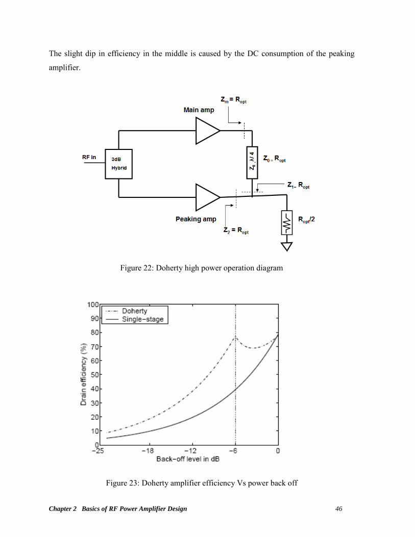
Chapter 2 Basics of RF Power Amplifier Design 46
The slight dip in efficiency in the middle is caused by the DC consumption of the peaking
amplifier.
Figure 22: Doherty high power operation diagram
Figure 23: Doherty amplifier efficiency Vs power back off

Chapter 2 Basics of RF Power Amplifier Design 47
2.6 Conclusion
The Doherty technique has already been implemented using a variety of device technologies,
predominantly using LDMOS and GaAs. With these technologies, the reported efficiency
numbers have been lower than the theoretical efficiencies, especially at frequencies higher
than 2.5GHz.Emerging device technologies such as the GaN technology presents an attrac-
tive option for Doherty design due its low output capacitance and high output impedance.
This aspect of GaN devices simplify the matching networks significantly, which makes it a
more favorable option when implementing a PA design on a very small design real estate of
an IC. Therefore, in this thesis GaN power cells are used to implement the Doherty design.
Detailed discussion on the GaN HFET technology would be discussed in Chapter 3.

Chapter 3 Semiconductor Technology Selection and GaN Large-Signal Model Evaluation 48
Chapter 3 Semiconductor Technology Selection and GaN
Large-Signal Model Evaluation
3.1 Semiconductor Technology selection
The RF power amplifier, a key module of a base station, can be designed using transistors
from a wide variety of semiconductor technologies. Apart from the performance specifica-
tions as output power, efficiency, and linearity, there are additional requirements that a power
amplifier transistor needs to consider, such as supply voltage, ruggedness, physical size, reli-
ability, and cost. Depending on the modulation format of the wireless system, the transistors
for the power amplifier may have different specifications. An excellent study comparing the
performance of RF output devices from various device technologies such as InGaP HBT,
EpHEMT, Si BJT, SiGe HBT, and Si LDMOS technologies for GSM, CDMA, and WCDMA
applications is presented in [43, 44].
A broad range of semiconductor technologies, such as Si LDMOS FET, Si BJT, GaN HFET,
GaAs MESFET, GaAs HEMT, and GaAs HBT have been used to design RF power amplifi-
ers. The type of semiconductor technology plays a critical role in the RF power amplifier per-
formance. Each of the technologies has its strengths and limitations. For instance, if GaAs
HBT, GaAs FET and LDMOS FET are compared, following can be observed; GaAs HBT's
have the highest power density which leads to the smallest amplifier die size, GaAs FET's
have lower RF power density but has higher power gain and PAE. Even though Si LDMOS
FETs have the lowest power densities leading to the largest die sizes they are the lowest in
cost [45]. In general, Si LDMOS FET’s are much more rugged as well [45]. Ruggedness of
an amplifier is its ability to survive large load mismatches, while delivering the rated output
power.
Another requirement that has been growing in demand is the thermal stability of high power
RF devices. Most common power devices that are currently used are Si LDMOS FETs and

Chapter 3 Semiconductor Technology Selection and GaN Large-Signal Model Evaluation 49
GaAS MESFETs. These device technologies are reaching their maximum capabilities. Hence
more emphasis has been placed on research and material processing technologies for device
technologies like SiC MESFET and GaN HEMT [46] [47]. Among these, GaN devices pro-
duce higher output power and power efficiency [47]. GaN device technology has greater ad-
vantages beyond other materials such as GaAs, SiC and Si, not only in terms of high power
but also the range of frequency operation [30]. The wide bandwidth is achieved in GaN due
to higher input and output impedances. Higher power is achieved due to the high charge den-
sity of the material.
The Doherty power amplifier architecture on MMICs has been implemented using various
device technologies, predominantly using Si-LDMOS [48] and GaAs [49] devices. But the
efficiencies achieved at frequencies, especially higher than 2.1GHz has been lower than theo-
retical efficiencies. Hence, newer device technologies like GaN should be further analyzed to
achieve maximum possible efficiency. The GaN technology presents an attractive option for
MMIC Doherty design, due to its high power density, higher efficiencies at high frequencies,
and high output impedance which can simplify the matching network significantly.
The next section of this chapter will present an overview of GaN material properties. A com-
parison of GaN properties to some other semiconductors as Si and GaAs will also be dis-
cussed. Some commonly known limitations and issues with the GaN technology will be pro-
vided in section 3.1.2
3.1.1 GaN properties
The most important properties of a semiconductor material that influences the power amplifi-
er performance are the breakdown field, thermal conductivity, energy band-gap, and electron
velocity [50]. Table 1 is a quick summary of how each of these material properties can influ-
ence the power amplifier system performance. As seen in that table, there is a direct relation-
ship between the material properties, device characteristics and power amplifier system per-
formance. Therefore, it is critical to select the appropriate device technology to meet the
power amplifier design requirements. Several of these material properties of common semi-
conductor materials as Si, GaAs, and GaN are summarized in table 2.

Chapter 3 Semiconductor Technology Selection and GaN Large-Signal Model Evaluation 50
Table 1: Semiconductor material properties and their relationship with power amplifier sys-tem performance [50].
Material property
Device characteristics
Improved device metrics System Advantages
High breakdown
field
High voltage
High
doping
Power density Gain
Efficiency
Larger output impedance
levels
The higher power density will reduce the number of die used
Improved output impedance characteris-tics with lead to increased bandwidth Higher efficiency will lead to lower
total energy usage
Wide Band-gap
High
Thermal Conductivity
High temperature
Smaller die size
More power
per die
High Thermal conductivity will allow the possibility of smaller packages and will reduce the system cooling require-
ments. The band-gap determines the upper
temperature limit of device operation. Hence, wider band gap devices are able to withstand higher channel and ambi-
ent temperatures, which will also reduce the system cooling requirements
High Electron Velocity
High Frequency
High ft
High fmax
High electron velocities will contribute to a very high speed device which re-
sults in high system frequencies
Table 2: Material Properties of GaN, Si and GaAs [50]
Property GaN Si GaAs
Band-gap (eV) 3.4 1.11 1.43 Breakdown field (V/cm) 35 x 105 7 x 10⁵ 7x 10⁵
Saturation velocity (cm/sec) 1.5 x 10⁷ 1x 10⁷ 1x 10⁷ Saturation field (V/cm) 15 x 103 8 x 10³ 3 x 10³
Thermal conductivity (W/cm-K) 1.7/substrate* 1.5 0.46 Electron mobility (Cm2/V-sec) 1000 1350 6000
Hole mobility (Cm2/V-sec) 300 450 330
*Refer to section 3.1.1 for details on GaN substrate materials
Chapter 3 Semiconductor Technology Selection and GaN Large-Signal Model Evaluation 51
From the table above, it can be seen that GaN has material properties that would be suitable
for high power implementations. For instance GaN has breakdown fields five times that of Si
or GaAs. Breakdown field determines the highest operating voltage of a transistor for a given
device design and channel doping [50]. Higher operating voltage results in higher power
handling capabilities and higher power density in the device. Due to this GaN devices can be
operated with high drain voltages since its break down voltages are greater than 70V [19].
GaN also has a large band-gap of 3.4 e V compared to Si, GaAs .This gives GaN an ad-
vantage in high temperature performance over Si and GaAs, since the band-gap determines
the upper temperature limit of device operation. For this reason, GaN devices would be able
to withstand higher ambient and channel temperatures. GaN can operate at higher channel
temperatures up to 300 0C [19].
GaN has a saturated electron velocity of 1.5 x 107cm/second, which is still higher than that of
Si or GaAs. The saturated electron velocity of device determines the frequency performance,
in particular, ft of a device [50]. Due to this high cut off frequency, GaN is able to operate at
frequencies much higher than Si and GaAs.
Note that GaN have electron and hole mobilities much less than Si and GaAs. Low mobility
results in increased parasitic resistance, increased losses, and reduced gain [50]. These prob-
lems are worsened as operating frequency is increased. Therefore when using a GaN device
for a power amplifier design, it is important to keep in mind the lower gain of the amplifier
path, so driver amplifiers may be included in the link budget to compensate for the low gain.
GaN devices have been grown on a number of different substrates such as Silicon (Si), Sili-
con carbide (SiC) and Sapphire. Compared to other available substrate choices, Sapphire is
relatively cheap and is offered in large diameter (4″ to 6″) wafers [50]. At microwave fre-
quencies it works great as a low-loss substrate. However due its low thermal conductivity of
0.46 W/cmK Sapphire will severely limit the power density and total power performance of
devices fabricated on it [50].SiC on the other hand has a thermal conductivity of 4.9 W/cm-K
that is three times that of Si and ten times that of Sapphire. This gives a tremendous ad-
vantage for SiC-based devices. SiC also have much better microwave performance than de-
vices fabricated on highly doped silicon substrates [50].The best GaN performance has been
from devices utilizing semi-insulating SiC substrates [50]. Although GaN-on-Si platform
Chapter 3 Semiconductor Technology Selection and GaN Large-Signal Model Evaluation 52
technology is not as mature, efforts are now focused on continual evolution of this technolo-
gy.
The resulting GaN-on-Si device technology offers high power performance at high levels of
reliability and is ideally suited for large area RF circuits. Compared to SiC, it is also less
costly and is in high volume production today and readily available [30].The cost of a high
resistivity silicon substrates is a fraction of the cost of 2” high resistivity SiC substrates
which are limited in quality, volume and availability [30].Based on the reliability results of
GaN-on-Si, it has been shown that that GaN-on-Si offers superior reliability to other sub-
strates [30].
3.1.2 GaN issues and limitations
Despite all the great characteristics of GaN devices, this device technology is still not mature
and has various issues that are still being addressed. The main reported problems of GaN de-
vices are current collapse, drain current compression and frequency dispersion of transcon-
ductance and capacitances [50 - 53]. These issues of GaN devices have been attributed pri-
marily due to the trapping effects. Trapping effects can be described as the surface trapping-
detrapping of electrons at the various surface states or trap states in the GaN structure [50,
53]. Trap states refer to the deep level states in the band-gap [19]. Detailed discussion of the
GaN device trapping and de-trapping process is presented in [51].These trap states induce
power loss, degrade power handling capability and causes voltage delays in device operation
[51]. Current collapse or current dispersion can be described as discrepancy between the DC
predicted and RF measured performance [53]. This phenomena leads to changes in the max-
imum drain current and knee voltage. These result in a change of load line and reduced pow-
er and gain. Any type of DC-to-RF dispersion causes device degradation and makes circuit
design very difficult. Various solutions to minimize some these problems have been pro-
posed. An overview of these proposals can be found in [53].
Despite these limitations of GaN, outstanding device performance (i.e reported fmax = 139
GHz and power densities of 30 W/mm [50]), can be seen from this relatively immature tech-
nology. Any performance limiting effects will have to be eliminated for these devices to
move from research to mass production.

Chapter 3 Semiconductor Technology Selection and GaN Large-Signal Model Evaluation 53
3.1.3 GaN MMIC process
The technology being explored in this project is Gallium Nitride (GaN)-based Heterostruc-
ture field-effect transistor (HFET) technology offered by the Canadian Photonics Fabrication
Centre (CPFC) of National Research Council (NRC). It is fabricated on 3-inch diameter Sili-
con Carbide (SiC) wafer. This MMIC circuit process of the HFET involves a total of nine
mask steps. The overall process includes a standard GaN device process. Thorough explana-
tion of process details can be found in [78]. The layer numbers in the foundry is used to de-
fine the mask levels used at the various steps of the process. In total there are 9 layers [78]:
• Layer 1-Mesa
• Layer 2-Ohmic
• Layer 3-Gate
• Layer 4-Via1
• Layer 5-Nichrome
• Layer 6-1Me
• Layer 7-Via2
• Layer 8-Bridge
• Layer 9-2Me
The process sequence steps applied to the HFET is described in the GaN foundry user manu-
al as follows [78]:
1. In the fundamental stage in the processing of the device, the Ohmic contact is defined
using the Ohmic mask and the contacts are deposited.
2. The second step in the process is the definition of the active area of the devices using
the Mesa mask, and etching the area outside it down to the buffer layer.
3. In the third step the gate metal in the channel area is deposited using the Gate mask.
4. The wafers are then passivated using a thin layer of dielectric. This is a critical layer
since it modifies the electrical properties of the surface of the AlGaN layer and pro-
vides added isolation between the substrate and metal layers after. Via1 mask is used
to define openings in a resist layer to etch the needed openings into the dielectric.
5. Next a thin layer of Nichrome is deposited where resistors are required.

Chapter 3 Semiconductor Technology Selection and GaN Large-Signal Model Evaluation 54
6. 1μm of gold is used as the first level on interconnect metal. It is deposited using the
1Me mask. The 1Me has contacts to the gate pads, the nichrome layer and the ohmic
metal.
7. Then a thin layer of dielectric is deposited to be used as the insulator in the MIM ca-
pacitors. The Via2 mask is used to define the vias for the openings in this layer.
8. In the next step, a second level of interconnect is introduced to bridge over other lay-
ers. It is defined in a temporary layer of a special resist using the Bridge mask.
9. In this step, another layer of interconnect is defined using the 2Me mask. This layer is
usually 1 μm of gold. 2Me is used to make the top layer of the MIM capacitors.
3.2 Conclusion
In conclusion, Gallium Nitride (GaN) is a new device technology that shows greater ad-
vantages beyond other materials such as GaAs and Si LDMOS for RF power amplifier de-
sign. Silicon LDMOS performance drops off as the frequency of operation increases to
>2.5GHz while GaAs suffers from low power even though it has potential to operate at high
frequency. This can be seen by the comparisons shown in figure 24 and figure 25. The mate-
rial properties of GaN produce devices that have high breakdown voltages and high power
densities that can operate at higher frequencies. This results in low parasitic capacitance and
high input and output impedances. High impedance levels and low output capacitance plays
an essential role in designing broadband amplifiers that are highly linear and efficient.
Figure 24: Comparison of highest reported ft and fmax for different RF device technologies
[50]

Chapter 3 Semiconductor Technology Selection and GaN Large-Signal Model Evaluation 55
Figure 25: Comparison of RF power density for different RF device technologies [50]
3.3 Transistor model evaluation with a Single stage GaN PA de-
sign using CGH25120F
Power amplifier design is a multi-step design procedure that is complex. Through the use of
accurate and reliable large-signal device models, the design process can be carried out from
start to end and the designer can have a reasonable idea of what to expect when the design is
fabricated.
The performance of the GaN MMIC Doherty amplifier designed in this thesis is assessed
based on the simulated performance using large-signal models. Hence, it was essential to as-
sess the accuracy and reliability of large-signal models for a new device technology as GaN
.It was crucial to perform an experiment to validate the large-signal models for GaN devices
by comparing the measured and simulated behavior of a GaN power amplifier design. There-
fore, in this section an analysis of a classical printed circuit board (PCB) design of a single
stage class AB amplifier using Cree’s CGH25120F GaN HEMT transistor will be presented.
A comparative analysis of the performance between the simulated data using the large signal
model of CGH25120F and measured data of the CGH25120F will be discussed.
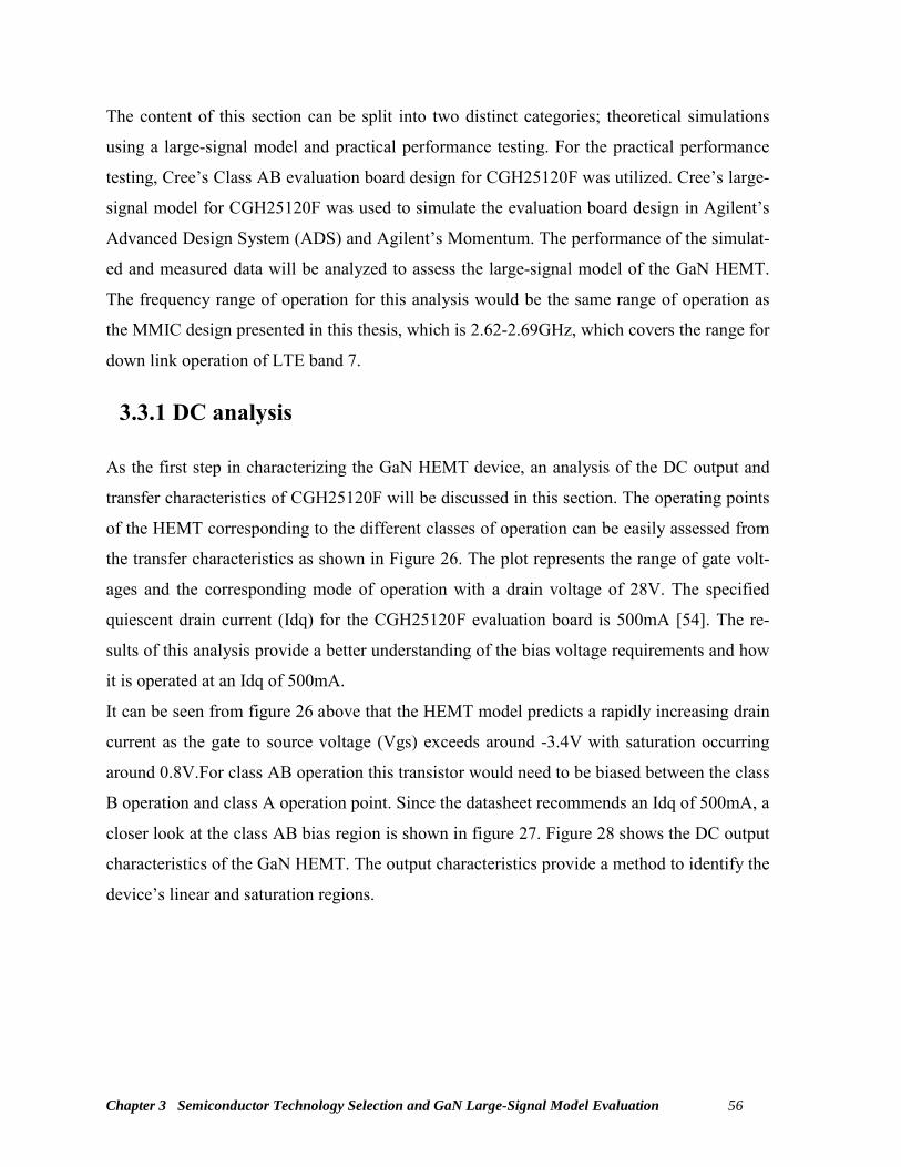
Chapter 3 Semiconductor Technology Selection and GaN Large-Signal Model Evaluation 56
The content of this section can be split into two distinct categories; theoretical simulations
using a large-signal model and practical performance testing. For the practical performance
testing, Cree’s Class AB evaluation board design for CGH25120F was utilized. Cree’s large-
signal model for CGH25120F was used to simulate the evaluation board design in Agilent’s
Advanced Design System (ADS) and Agilent’s Momentum. The performance of the simulat-
ed and measured data will be analyzed to assess the large-signal model of the GaN HEMT.
The frequency range of operation for this analysis would be the same range of operation as
the MMIC design presented in this thesis, which is 2.62-2.69GHz, which covers the range for
down link operation of LTE band 7.
3.3.1 DC analysis
As the first step in characterizing the GaN HEMT device, an analysis of the DC output and
transfer characteristics of CGH25120F will be discussed in this section. The operating points
of the HEMT corresponding to the different classes of operation can be easily assessed from
the transfer characteristics as shown in Figure 26. The plot represents the range of gate volt-
ages and the corresponding mode of operation with a drain voltage of 28V. The specified
quiescent drain current (Idq) for the CGH25120F evaluation board is 500mA [54]. The re-
sults of this analysis provide a better understanding of the bias voltage requirements and how
it is operated at an Idq of 500mA.
It can be seen from figure 26 above that the HEMT model predicts a rapidly increasing drain
current as the gate to source voltage (Vgs) exceeds around -3.4V with saturation occurring
around 0.8V.For class AB operation this transistor would need to be biased between the class
B operation and class A operation point. Since the datasheet recommends an Idq of 500mA, a
closer look at the class AB bias region is shown in figure 27. Figure 28 shows the DC output
characteristics of the GaN HEMT. The output characteristics provide a method to identify the
device’s linear and saturation regions.
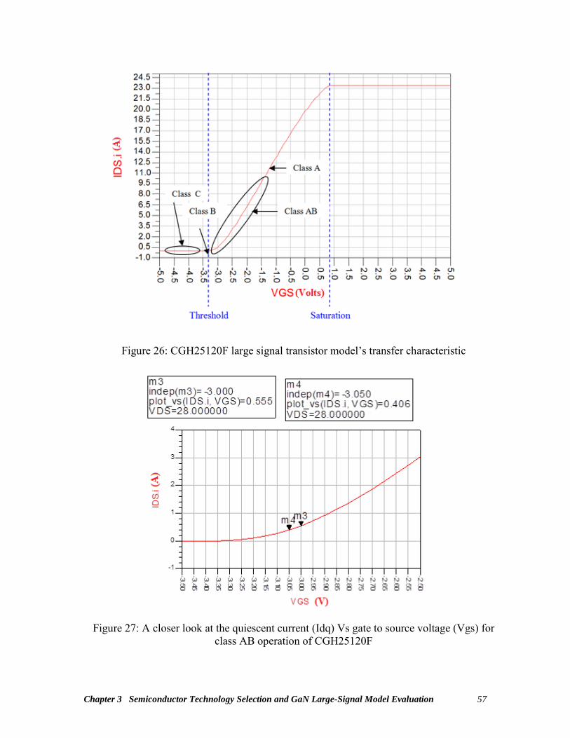
Chapter 3 Semiconductor Technology Selection and GaN Large-Signal Model Evaluation 57
Figure 26: CGH25120F large signal transistor model’s transfer characteristic
Figure 27: A closer look at the quiescent current (Idq) Vs gate to source voltage (Vgs) for
class AB operation of CGH25120F

Chapter 3 Semiconductor Technology Selection and GaN Large-Signal Model Evaluation 58
Figure 28: DC output characteristics of CGH25120F
Figure 29: Test bench for DC analysis of Cree’s CGH25120F large signal transistor model
The above graphs clearly indicate that the required Vgs to achieve an Idq of 500mA is
around -3.02V.Such an operating point will allow for class AB operation of the CGH25120F
GaN transistor. Note that during the practical measurements in the lab, a Vgs of -3.26V
needed be applied to achieve 500mA for a 28V supply voltage.
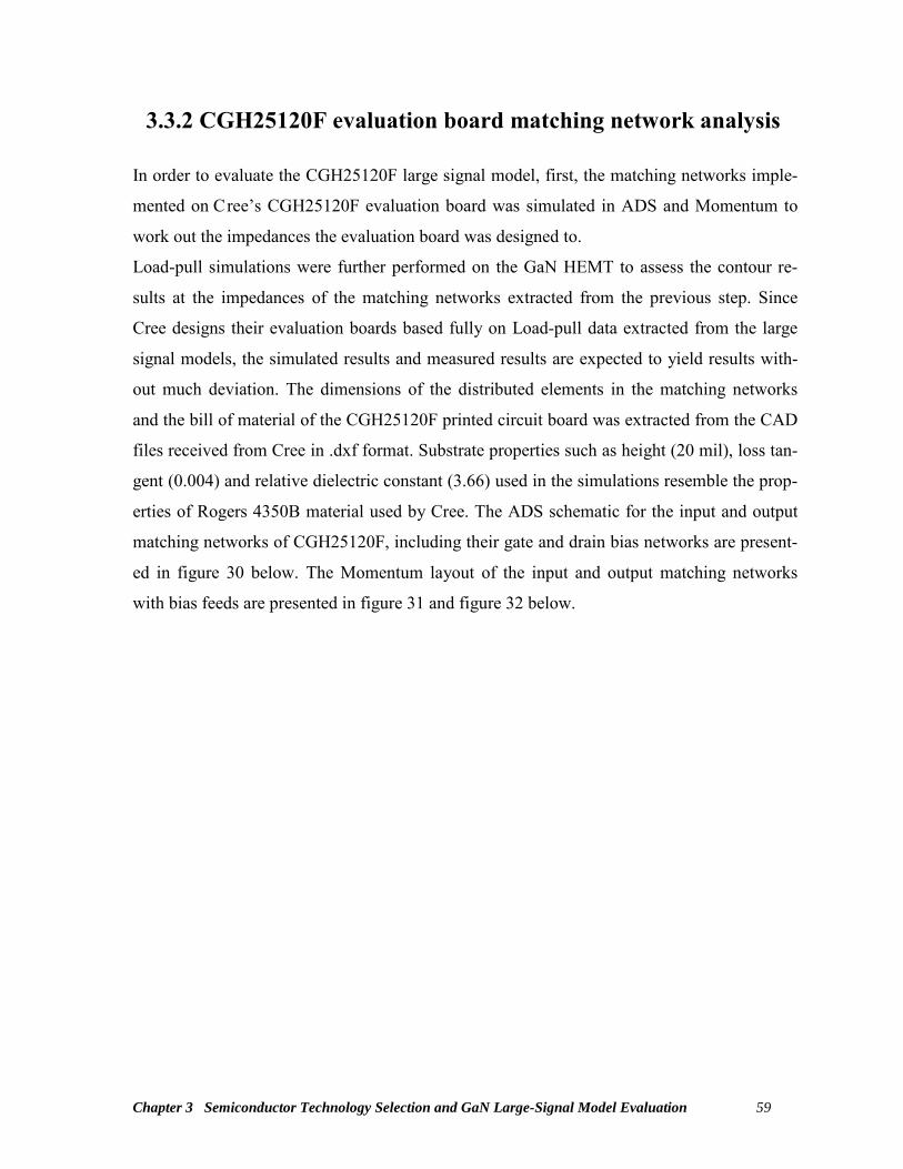
Chapter 3 Semiconductor Technology Selection and GaN Large-Signal Model Evaluation 59
3.3.2 CGH25120F evaluation board matching network analysis
In order to evaluate the CGH25120F large signal model, first, the matching networks imple-
mented on Cree’s CGH25120F evaluation board was simulated in ADS and Momentum to
work out the impedances the evaluation board was designed to.
Load-pull simulations were further performed on the GaN HEMT to assess the contour re-
sults at the impedances of the matching networks extracted from the previous step. Since
Cree designs their evaluation boards based fully on Load-pull data extracted from the large
signal models, the simulated results and measured results are expected to yield results with-
out much deviation. The dimensions of the distributed elements in the matching networks
and the bill of material of the CGH25120F printed circuit board was extracted from the CAD
files received from Cree in .dxf format. Substrate properties such as height (20 mil), loss tan-
gent (0.004) and relative dielectric constant (3.66) used in the simulations resemble the prop-
erties of Rogers 4350B material used by Cree. The ADS schematic for the input and output
matching networks of CGH25120F, including their gate and drain bias networks are present-
ed in figure 30 below. The Momentum layout of the input and output matching networks
with bias feeds are presented in figure 31 and figure 32 below.

Chapter 3 Semiconductor Technology Selection and GaN Large-Signal Model Evaluation 60
(a)
Impedance seen by the gate
vgbias
INP
UT
Do not delete
this port.
\"Lower\"
Bias
Port
InputP
ortM
LOC
TL20
L=50 m
ilW
=100 m
ilS
ubst="M
Sub1"
MLO
CT
L14
L=39.2 m
ilW
=125 m
ilS
ubst="M
Sub1"
sc_spr_595D_B
016_X9_19960828
C5
PA
RT
_NU
M=
595D106X
9016B7 10uF
MLIN
TL35
L=110 m
ilW
=167 m
ilS
ubst="M
Sub1"
MLIN
TL34
L=441 m
ilW
=100 m
ilS
ubst="M
Sub1"
MC
OR
NC
orn3
W=
50 mil
Subst=
"MS
ub1"
Port
vgbiasN
um=
4M
LINT
L36
L=10 m
ilW
=50 m
ilS
ubst="M
Sub1"
MT
EE
_AD
ST
ee9
W3=
167 mil
W2=
50 mil
W1=
50 mil
Subst=
"MS
ub1"
MLIN
TL9
L=70 m
ilW
=50 m
ilS
ubst="M
Sub1"
MLIN
TL10
L=282 m
ilW
=50 m
ilS
ubst="M
Sub1"
MC
OR
NC
orn1
W=
50 mil
Subst=
"MS
ub1"M
LINT
L11
L=255 m
ilW
=50 m
ilS
ubst="M
Sub1"
MT
EE
_AD
ST
ee5
W3=
50 mil
W2=
50 mil
W1=
50 mil
Subst=
"MS
ub1"
MLIN
TL25
L=10 m
ilW
=50 m
ilS
ubst="M
Sub1"
RR2
R=
5.1 Ohm
MLIN
TL27
L=24 m
ilW
=50 m
ilS
ubst="M
Sub1"
MT
EE
_AD
ST
ee6
W3=
50 mil
W2=
50 mil
W1=
50 mil
Subst=
"MS
ub1"
MLIN
TL26
L=10 m
ilW
=50 m
ilS
ubst="M
Sub1"
MT
EE
_AD
ST
ee7
W3=
50 mil
W2=
50 mil
W1=
50 mil
Subst=
"MS
ub1"
MLIN
TL29
L=10 m
ilW
=50 m
ilS
ubst="M
Sub1" M
LINT
L28
L=375.5 m
ilW
=50 m
ilS
ubst="M
Sub1"
MLIN
TL31
L=18 m
ilW
=50 m
ilS
ubst="M
Sub1"
MT
EE
_AD
ST
ee8
W3=
50 mil
W2=
50 mil
W1=
50 mil
Subst=
"MS
ub1"
MLIN
TL32
L=262 m
ilW
=50 m
ilS
ubst="M
Sub1"
MC
OR
NC
orn2
W=
50 mil
Subst=
"MS
ub1"
sc_kmt_X
7R_06035_J_19960828
C3
Tem
perature=25
Vtest=
1 P
AR
T_N
UM
=C
0603C471J5R
470pF
MLIN
TL33
L=47 m
ilW
=50 m
ilS
ubst="M
Sub1"
MLIN
TL30
L=10 m
ilW
=50 m
ilS
ubst="M
Sub1"
sc_kmt_X
7R_08055_J_19960828
C4
Tem
perature=25
Vtest=
1 P
AR
T_N
UM
=C
0805C333J5R
33nF
SR
LCS
RLC
3
C=
8.2 pFL=
0.15 nHR
=0.127 O
hmS
RLC
SR
LC5
C=
82 pFL=
0.12 nHR
=0.119 O
hm
MLIN
TL37
L=40 m
ilW
=42.5 m
ilS
ubst="M
Sub1"
MLIN
TL19
L=40 m
ilW
=42.5 m
ilS
ubst="M
Sub1"
Port
INP
UT
Num
=1
MLIN
TL23
L=37 m
ilW
=530 m
ilS
ubst="M
Sub1"
MLIN
TL17
L=30 m
ilW
=10 m
ilS
ubst="M
Sub1"
MLIN
TL16
L=30 m
ilW
=10 m
ilS
ubst="M
Sub1"
RR1
R=
150 Ohm
SR
LCS
RLC
2
C=
27 pFL=
0.14 nHR
=0.135 O
hm
SR
LCS
RLC
1
C=
6.8 pFL=
0.16 nHR
=0.13 O
hm
MLIN
TL8
L=480 m
ilW
=42.5 m
ilS
ubst="M
Sub1"
MLO
CT
L21
L=40 m
ilW
=125 m
ilS
ubst="M
Sub1"
MC
RO
SO
Cros1
W4=
125 mil
W3=
42.5 mil
W2=
125 mil
W1=
42.5 mil
Subst=
"MS
ub1"
MLIN
TL7
L=69 m
ilW
=42.5 m
ilS
ubst="M
Sub1"
MLIN
TL6
L=70 m
ilW
=42 m
ilS
ubst="M
Sub1"
MT
EE
_AD
ST
ee4
W3=
100 mil
W2=
42 mil
W1=
42 mil
Subst=
"MS
ub1"
MLIN
TL5
L=462 m
ilW
=42 m
ilS
ubst="M
Sub1"
MT
EE
_AD
ST
ee2
W3=
10 mil
W2=
42 mil
W1=
42 mil
Subst=
"MS
ub1"
MLIN
TL24
L=32.5 m
ilW
=42 m
ilS
ubst="M
Sub1"
MLIN
TL2
L=32.5 m
ilW
=42 m
ilS
ubst="M
Sub1"
MT
EE
_AD
ST
ee1
W3=
10 mil
W2=
42 mil
W1=
42 mil
Subst=
"MS
ub1"
MLIN
TL1
L=145 m
ilW
=42 m
ilS
ubst="M
Sub1"
MT
EE
_AD
ST
ee3
W3=
50 mil
W2=
530 mil
W1=
530 mil
Subst=
"MS
ub1"
MLIN
TL22
L=113 m
ilW
=530 m
ilS
ubst="M
Sub1"
MS
TE
PS
tep1
W2=
530 mil
W1=
42.5 mil
Subst=
"MS
ub1"
CG
H25120F
_r6_CG
H25_r6
X1
crth=1.5
tcase=25
Cree C
GH
25120F

Chapter 3 Semiconductor Technology Selection and GaN Large-Signal Model Evaluation 61
(b)
Figure 30: ADS schematic of CGH25120F evaluation board matching networks ; (a)
input matching (b) output matching
Impedance seen by the drain
vdbias
Do not delete
this port.
OU
TP
UT
Do not delete
this port.
Port
vdbiasN
um=
3
sc_spr_293D_B
025_X9_19960828
C24
PA
RT
_NU
M=
293D105X
9025B2 1.0uF
MLIN
TL96
L=10 m
ilW
=120 m
ilS
ubst="M
Sub1"
sc_kmt_X
7R_06035_J_19960828
C23
Tem
perature=25
Vtest=
1 P
AR
T_N
UM
=C
0603C471J5R
470pF
MLIN
TL95
L=37 m
ilW
=530 m
ilS
ubst="M
Sub1"
MC
RO
SO
Cros4
W4=
50 mil
W3=
530 mil
W2=
50 mil
W1=
530 mil
Subst=
"MS
ub1"
MLIN
TL122
L=335 m
ilW
=530 m
ilS
ubst="M
Sub1"
MS
TE
PS
tep6
W2=
100 mil
W1=
530 mil
Subst=
"MS
ub1"
MC
OR
NC
orn9
W=
50 mil
Subst=
"MS
ub1"
MLIN
TL112
L=430 m
ilW
=50 m
ilS
ubst="M
Sub1"
MLIN
TL104
L=608 m
ilW
=100 m
ilS
ubst="M
Sub1"
SR
LCS
RLC
23
C=
24 pFL=
0.17 nHR
=0.037 O
hm
MLIN
TL108
L=51 m
ilW
=60 m
ilS
ubst="M
Sub1"
MLIN
TL109
L=51 m
ilW
=60 m
ilS
ubst="M
Sub1"
MS
TE
PS
tep5
W2=
42 mil
W1=
100 mil
Subst=
"MS
ub1"
MLIN
TL120
L=328 m
ilW
=42 m
ilS
ubst="M
Sub1"
MLIN
TL121
L=321 m
ilW
=42 m
ilS
ubst="M
Sub1"
sc_spr_293D_B
025_X9_19960828
C25
PA
RT
_NU
M=
293D105X
9025B2 1.0uF
sc_kmt_X
7R_08055_J_19960828
C26
Tem
perature=25
Vtest=
1 P
AR
T_N
UM
=C
0805C333J5R
33nF
SR
LCS
RLC
22
C=
8.2 pFL=
0.15 nHR
=0.127 O
hm
MLIN
TL101
L=10 m
ilW
=120 m
ilS
ubst="M
Sub1"
MLIN
TL102
L=10 m
ilW
=71 m
ilS
ubst="M
Sub1"
MLIN
TL103
L=10 m
ilW
=51 m
ilS
ubst="M
Sub1"
MT
EE
_AD
ST
ee28
W3=
120 mil
W2=
50 mil
W1=
50 mil
Subst=
"MS
ub1"
MT
EE
_AD
ST
ee29
W3=
71 mil
W2=
50 mil
W1=
50 mil
Subst=
"MS
ub1"
MLIN
TL110
L=24 m
ilW
=50 m
ilS
ubst="M
Sub1"
MT
EE
_AD
ST
ee30
W3=
51 mil
W2=
50 mil
W1=
50 mil
Subst=
"MS
ub1"
MLIN
TL111
L=24 m
ilW
=50 m
ilS
ubst="M
Sub1"
Port
OU
TP
UT
Num
=2
MLIN
TL119
L=24 m
ilW
=50 m
ilS
ubst="M
Sub1"
MC
OR
NC
orn10
W=
50 mil
Subst=
"MS
ub1"
MLIN
TL118
L=330 m
ilW
=50 m
ilS
ubst="M
Sub1"
MLIN
TL117
L=315 m
ilW
=50 m
ilS
ubst="M
Sub1"
MT
EE
_AD
ST
ee35
W3=
51 mil
W2=
50 mil
W1=
50 mil
Subst=
"MS
ub1"
MT
EE
_AD
ST
ee34
W3=
51 mil
W2=
50 mil
W1=
50 mil
Subst=
"MS
ub1"
MLIN
TL116
L=24 m
ilW
=50 m
ilS
ubst="M
Sub1"
MT
EE
_AD
ST
ee33
W3=
51 mil
W2=
50 mil
W1=
50 mil
Subst=
"MS
ub1"
MLIN
TL115
L=24 m
ilW
=50 m
ilS
ubst="M
Sub1"
MT
EE
_AD
ST
ee32
W3=
69 mil
W2=
50 mil
W1=
50 mil
Subst=
"MS
ub1"
MLIN
TL113
L=28 m
ilW
=120 m
ilS
ubst="M
Sub1"
MT
EE
_AD
ST
ee31
W3=
120 mil
W2=
120 mil
W1=
120 mil
Subst=
"MS
ub1"
MLIN
TL100
L=10 m
ilW
=51 m
ilS
ubst="M
Sub1"
MLIN
TL99
L=10 m
ilW
=51 m
ilS
ubst="M
Sub1"
MLIN
TL98
L=10 m
ilW
=51 m
ilS
ubst="M
Sub1"
MLIN
TL97
L=10 m
ilW
=69 m
ilS
ubst="M
Sub1"
SR
LCS
RLC
21
C=
8.2 pFL=
0.15 nHR
=0.127 O
hm
sc_kmt_X
7R_08055_J_19960828
C22
Tem
perature=25
Vtest=
1 P
AR
T_N
UM
=C
0805C333J5R
33nFS
RLC
SR
LC20
C=
82 pFL=
0.12 nHR
=0.119 O
hm
CG
H25120F
_r6_CG
H25_r6
X1
crth=1.5
tcase=25
Cree C
GH
25120F

Chapter 3 Semiconductor Technology Selection and GaN Large-Signal Model Evaluation 62
Figure 31: Layout of CGH25120F evaluation board input matching network with bias feeds
Figure 32: Layout of CGH25120F evaluation board output matching network with bias feeds Table 3 summarizes the measured and simulated gate and drain impedances achieved at
2.650GHz.

Chapter 3 Semiconductor Technology Selection and GaN Large-Signal Model Evaluation 63
Table 3: Comparison of measured and simulated impedances of CGH25120F
Datasheet measured impedance of the
evaluation board at 2.650GHz
Impedance of the simulated structure with Momentum
at 2.650GHz
Impedance of the simulated structure
with ADS at 2.650GHz
Impedance seen by the device gate 4.39-10.3j 4.32-10.9j 4.04-12.8j
Impedance seen by the device drain 3.98-1.37j 3.35-2.87j 4.22-2.53j
From this table, it can be been that both momentum and ADS simulations provide close im-
pedances to the measured impedances stated on the datasheet [54] for the CGH25120F eval-
uation board. Since momentum simulations would provide the closest estimation of the actu-
al effects of the copper structures, for further assessment of the CGH25120F large signal
model, the evaluation was carried out in co-simulation using momentum structures. The dif-
ferences in the datasheet stated impedances versus the simulated impedances could be due to
several reasons. If the output matching structure of the datasheet is compared to the output
structure of the evaluation board , it can be seen that the datasheet output structure is slightly
different; it has an additional open stub in the matching network (refer to figure 73 and figure
73 in Appendix A) which would change the impedance seen by the device. The lumped com-
ponent models may not model all parasitic effects which would also alter the impedances.
Load-pull simulations are an important step to understand the behavior of a large signal mod-
el. The optimum impedance of a device can be extracted through non-linear simulations if
accurate large signal models are available. Agilent’s ADS Load-pull simulations show the
performance of the large signal model under different load conditions using harmonic bal-
ance (HB) analysis.
Load-pull simulations performed on C ree’s CGH25120F large signal model are shown in
figure 33 and figure 34. Single tone simulations were performed with fundamental source
(Zs) impedance of 4.32-10.9j, drain voltage of 28V and gate voltage of -3.02V to achieve an
Idq of 500mA at 2.650GHz. At the given bias point, input power and frequency, output pow-
er contours elliptically in a 0.6dB step and power added efficiency in a 5% step.

Chapter 3 Semiconductor Technology Selection and GaN Large-Signal Model Evaluation 64
Figure 33: Simulated efficiency and power delivered Load-pull contours at the load imped-ance from the simulated momentum structures for CGH25120F evaluation board
Figure 33 shows the simulated contour lines for Power added efficiency (PAE) and power
delivered to the load (Pdel).Although the highest achievable efficiency for this device is
55.97%, the evaluation board has been designed at an impedance of 3.35-2.87j where t he
efficiency is around 40% at an output power of 46dBm. This indicates that the impedance has
been selected to have a good compromise between linearity and efficiency. This assumption
can be further established by observing the IMD3 contours extracted from the two-tone
Load-pull simulations. From figure 34 it can be seen that, although the PAE and Pdel con-
tours rotate in the same direction, the IMD3 contours rotate differently. This indicates that a
higher efficiency impedance point could yield lower linearity.

Chapter 3 Semiconductor Technology Selection and GaN Large-Signal Model Evaluation 65
Figure 34: Simulated IMD3, efficiency and power delivered Load-pull contours from the simulated momentum structures for CGH25120F evaluation board
3.3.3 Comparison of Measured and Simulated Performance of
CGH25120F
In order to determine the performance of the CGH25120F large signal model, gain, drain ef-
ficiency and compression points have been characterized with the measured and simulated
test setups. The simple measurement setup for such characterization includes a power meter,
signal generator and power supplies as shown in figure 35. The measurement setup has been
fully calibrated to accurately determine the large signal performance. An image of the actual
setup can be found in appendix C. Table 4 summarizes the simulated and measured data col-
lected at the centre band of 2.65GHz.
Table 4: Measured and simulated performance data of the CGH25120F evaluation board
P3 dB (dBm)
Gain(dB) at 2.65GHz for Pout of 46dBm
Drain efficiency at 2.65GHz for Pout of 46dBm
Simulated 50.4 14.03 39.9 % Measured 51.2 13.68 45.03 %

Chapter 3 Semiconductor Technology Selection and GaN Large-Signal Model Evaluation 66
Figure 35: Measurement setup of CGH25120F evaluation board

Chapter 3 Semiconductor Technology Selection and GaN Large-Signal Model Evaluation 67
Analysis of the 3dB compression points and gain suggests that the simulated design provides
very close results to the measured results. Figure 36 depicts the compressions points of the
simulated and measured CGH25120F design. Measurements were performed with a pulsed
CW signal with a 12% duty cycle from the signal generator. Simulated performance has been
done using a single tone source. Note that although P1dB is the fundamental metric of esti-
mating linearity of an amplifier, for some devices types with certain characteristics, assessing
the P1dB point may not be as apparent. For instance, due to the smooth transition from the
linear to the saturation region, GaN amplifiers typically define their output power at the 3dB
compression point. This can be clearly seen by the measured data in figure 36. The measured
and simulated 3dB compression points for the CGH25120F design only deviate by 0.8 dB.
Even though the simulated P3dB point is very close to the measured data, the large signal
model does not seem to model the true transition characteristics from the linear to the satura-
tion region of the device. The measured gain data depicted in figure 37 has been done using a
10MHz LTE signal with a 7dB PAR at 0.01% probability on CCDF. As revealed in figure
37, measured and simulated gain differs only by 0.4dB at the band centre (2.65GHz). Alt-
hough, the simulated gain predicts a flat response for the full band of 2.62-2.69GHz, the
measured gain shows a roll off around 0.5dB at the band edges.
Again, the large signal model fails to fully predict the over frequency response of the
CGH25120F design. In figure 38, the measured and simulated drain efficiency is shown to be
different by approximately 5%, where the measured data shows the higher efficiency of 45%.
Overall, the large signal simulations predicted the gain and P3dB performance quite well.
Although the simulated efficiency results were 5% less than the actual measurements, the
large signal model does give a good indication of the expected measured performance. What
the large signal model seem to lack is to accurately predict the over frequency and over pow-
er performance of the device. Other factors can also contribute to the difference in the meas-
ured over frequency response, that may not be captured in the simulated environment accu-
rately, such as coupling effects, parasitic effects of the lumped elements, SMA connector im-
pacts and so on.

Chapter 3 Semiconductor Technology Selection and GaN Large-Signal Model Evaluation 68
10
11
12
13
14
15
16
40 41 42 43 44 45 46 47 48 49 50 51 52 53 54 55
Pout (dBm)
Gai
n (d
B) Measured @ 2.62GHz
Measured @ 2.65GHzMeasured @ 2.69GHzSimulated @ 2.65GHz
P3 dB for measured
P3 dB for simulated
CGH25120F measured and simulated gain compression curves
Figure 36: Measured and simulated compression curves for CGH25120F
CGH25120F measured and simulated gain over frequency
10
11
12
13
14
15
2.61 2.62 2.63 2.64 2.65 2.66 2.67 2.68 2.69 2.7
Freq (GHz)
Gai
n (d
B)
43dBm_measured46dBm_measured43dBm_simulated46dBm_simulated
Figure 37: Measured and simulated gain over frequency for CGH25120F
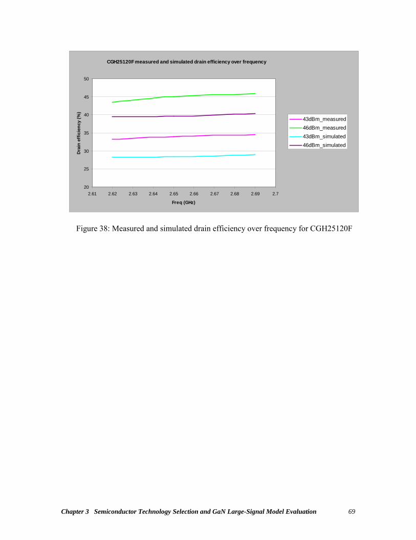
Chapter 3 Semiconductor Technology Selection and GaN Large-Signal Model Evaluation 69
CGH25120F measured and simulated drain efficiency over frequency
20
25
30
35
40
45
50
2.61 2.62 2.63 2.64 2.65 2.66 2.67 2.68 2.69 2.7
Freq (GHz)
Dra
in e
ffic
ienc
y (%
)
43dBm_measured46dBm_measured43dBm_simulated46dBm_simulated
Figure 38: Measured and simulated drain efficiency over frequency for CGH25120F

Chapter 4 Doherty Power Amplifier Design Implementation & Results 70
Chapter 4 Doherty Power Amplifier Design Implementa-
tion & Results
4.1 Doherty Amplifier Design for a 5W pico-cell base station
In this section a MMIC design of a Doherty power amplifier in Gallium Nitride (GaN) tran-
sistor technology will be provided. This entails a detailed design procedure of a two way
symmetrical Doherty amplifier for a 5W base station and its performance evaluation in LTE
band 7. A concise summary of the design procedure will be followed by the design, simula-
tion and characterization of the amplifier. It features a link budget analysis along with device
characterization, DC simulation, load pull characterization, design and optimization of bias
networks and matching circuits. Two 8 x 200µm GaN HFETs will be utilized for each main
and peaking amplifiers in Doherty configuration on a 10mm x 11.5mm chip. The design of a
Doherty amplifier is an intricate procedure that involves the design of several sub circuits
such as the main and peaking amplifiers, power combiner and divider networks. This section
will present the design of each sub circuit in detail and finally an analysis of the final
Doherty amplifier performance. Section 4.1.9 will present a discussion on the layout design
of the two-way Doherty amplifier. Results of the designed PA will be provided in section 4.2.
4.1.1 Design Specifications for LTE
The foremost step in designing a power amplifier is to specify the system requirements.
Since the goal of this thesis is to realize a Doherty power amplifier for LTE applications, the
specifications would be based on s tandards developed by the third generation partnership
project (3GPP).
LTE was introduced in 3GPP Rel8. Its radio access is referred to as Evolved UMTS terrestri-
al radio access network (E-UTRAN). LTE can use QPSK, 16QAM or 64QAM modulation
schemes, and can be either frequency division duplex (FDD) or time division duplex (TDD).

Chapter 4 Doherty Power Amplifier Design Implementation & Results 71
It can support up-to six different channel bandwidths of 1.4MHz, 3MHz, 5MHz, 10MHz,
15MHz, and 20MHz, which provides more deployment flexibility than previous systems.
According to 3GPP specifications, LTE can provide more than 100Mbps of maximum down-
link speed [6]. Although the traditional pico-cell base station output powers typically range
from around 200mW-1W [79], recently developed pico-cell base stations announced by ven-
dors such as Nokia Siemens Networks and Huawei are fairly large devices, with transmit
powers of 2 X 5W (2 X 37dBm)[84]. Hence, this project will focus on a power amplifier de-
sign that is suitable for a pico-cell base station with an output power of 5W.
Another important design parameter is the crest factor or the peak to average power ratio of
the signal (PAPR). The PAPR depends on the number of data channels being used. Therefore
higher data rates results in very high peak to average ratios. LTE offers variable data rates of
more than 100Mbps which result in large peak to average ratios of 6dB and higher at 0.01
clipping probability [80].
ACLR is another important design specification. There are two ACLR measurements in LTE,
E-UTRA ACLR and UTRA ACLR. E-UTRA uses LTE to LTE adjacent signal, and UTRA
ACLR uses LTE to WCDMA adjacent signal. The frequently used the limit for UTRA
ACLR is -36dBc and -33dBc for E-UTRA ACLR [81]. Often base station power amplifier
ACLR is measured on a system with a linearization technique such as digital pre-distortion,
where typical minimum correction is around 25dB. Hence, if the intent is to use the PA de-
sign with a linearization technique such as digital pre-distortion, less emphasis can be placed
on linearity during the design of the PA and trade-offs can be made to place more emphasis
on efficiency or gain. Design requirements for the pico-cell baste station power amplifier de-
signed in this project can be summarized in Table 5.
Table 5: Design requirements
Parameter Design specifications Operating Frequency (LTE Downlink operating band 7) [6] 2.62-2.69GHz
Base station average output power (Pout) 5W Power Amplifier average output power (PA Pout)* 40dBm
Gain at PA output >10dB Average power added efficiency (PAE) >35%
* Refer to section 4.1.3 for detailed calculations

Chapter 4 Doherty Power Amplifier Design Implementation & Results 72
4.1.2 Design procedure
Following design procedure was followed to realize the Doherty amplifier:
1. Determine the GaN HFET sizing (number of FETs, number of fingers, unity gate
width) to achieve the power required
2. Determine the bias point for the main and peaking amplifier to achieve the desired
operation in Doherty topology.
3. Design DC bias circuit.
4. Set the selected input impedance as the source impedance and load pull the device.
From the contours, determine output impedances required for low and high power re-
gions of operation. The load seen from the main amplifier at the low power region
when the peaking amplifier is still off should ensure maximum efficiency at a saturat-
ed output power 3dB less than the maximum PA output power as per Doherty opera-
tion discussed in chapter 2. The second main amplifier load for the high power region
should ideally assure maximum output power with roughly the same efficiency.
5. Once the desired loads have been found, design the output matching networks
6. Design input matching networks.
7. Design the Doherty combiner. Doherty output combiner consists of a quarter- wave
transmission line with the characteristic impedance of Ropt and a quarter-wave trans-
mission line that transforms from Ropt/2 to 50 Ohm, which is the required system out-
put impedance.
8. Complete Doherty PA design
a. Utilizing the designed input/output matching structures, combine the Class
AB and Class C biased amps with the Doherty combiner.
b. Adjust the main and peaking amplifier offset lines to optimize the perfor-
mance. Due to die and package parasitics and external matching circuits, the
required 2 Ropt interface at the main amplifier device plain in the low power
regime may not necessarily result in a purely resistive translation at the load
line, therefore phase compensation will typically be required to rotate the load
line impedance back to the real axis for the desired resistive load. Same ap-
plies for the peaking amplifier, which would also require an offset line. Note

Chapter 4 Doherty Power Amplifier Design Implementation & Results 73
that the offset lines will not affect the overall matching condition and load
modulation because they are matched to the characteristic impedance of 50
Ohm.
9. Verify out power, efficiency gain and other requirements of complete power amplifier
over frequency once layout components are realized in the design. Figure 39 below
summarizes the sub blocks required for the Doherty design procedure discussed
above.
Figure 39: Doherty Amplifier design blocks
4.1.3 Device Sizing
The required FET size (number of fingers x gate width) is dependent on the required power
amplifier output power, peak-to-average power ratio (PAPR) of the signal and the power
density of the device. The peak to average ratio depends on the number of data channels be-
ing used in a specific standard. LTE offers variable data rates which would result in peak to
average ratios of 6dB and higher .Therefore 6dB PAPR was selected to the estimate the re-
quirements for this project. Following calculations were performed to assess the device size.
Primary step is to assess the losses between the power amplifier and the base station antenna
to calculate the required output power from the Doherty amplifier. Typical worst case back
end losses at 2.6GHz would include microstrip losses (0.1dB) + directional coupler (used to
couple the output signal for linearization) insertion loss (0.3dB) + output circulator insertion

Chapter 4 Doherty Power Amplifier Design Implementation & Results 74
loss (0.3dB) + output connector loss (0.2dB) + duplexor filter insertion loss (2.1dB), which
would total to around 3.0 dB of losses. Hence to have an output power of 5W (37dBm) at the
pico-cell base station, the power amplifier average output power needs to be 37dBm + 3.0dB
= 40 dBm. Therefore the assumed average PA output power (Pavg) = 40 dBm and PAPR =
6dB. Typically amplifier devices are sized such that P1dB (dB) = Pavg + PAR = 40 + 6dBm
= 46dBm (40W). Therefore the total required device size would be 40W.
In a two way Doherty configuration each device size would be 40W /2 = 20W per
main/peaking amplifier. The Device power density can be calculated using the following:
Device power density = 2222
dssbreakdown IV× (4.22)
From the I-V curves of the GaN MMIC design foundry manual [78]: Vbreakdown = 100 V, Idss =
0.55A. Applying this to equation (4.22), would give a device power density of 6.875 W/mm.
Since the devices would be operating at a lower current than Idss, 6.5W/mm was used for the
estimation.
The required gate width would be = 20W / 6.5W = 3.08 mm
The largest gate fingers available in foundry = 8 x 200µm = 1.6 mm
Therefore the minimum number of 8 x 200µm cells required = 3.08 mm / 1.6mm = 1.92.
Thus, two 8 x 200µm cells per main and peaking amplifier were used. All simulations will be
performed using the ADS GaN MMIC design foundry provided by NRC.
4.1.4 DC analysis
The Doherty configuration requires two different biasing for the main and peaking stages
.Both main and peaking amplifiers are designed to deliver maximum power with optimum
efficiency at a specified load. Analysis of different classes of power amplifier shows that the
required performance of the main amplifier can be very closely achieved by biasing the tran-
sistor in Class AB or B mode of operation. The peak amplifier is made active only during the
peaks of the input signal and hence is designed to only amplify signals that cross a minimum
threshold. This is achieved by biasing the device below its pinch-off voltage for operation
similar to class C. For this project, the main amplifier was chosen to be biased in class AB
and the peaking in class C. The transfer characteristics and IV curves of the GaN HFET un-
der consideration is shown in figure 40 and figure 41 below.

Chapter 4 Doherty Power Amplifier Design Implementation & Results 75
-5.5-5.0-4.5-4.0-3.5-3.0-2.5-2.0-1.5-1.0-0.50.00.51.01.52.02.53.03.54.04.5
-6.0
5.0
0.4
0.8
1.2
1.6
2.0
2.4
2.8
3.2
0.0
3.6
VGS
IDS.
i
m2
m2indep(m2)=plot_vs(IDS.i, VGS)=0.156VDS=20.000000
-3.250
Figure 40: Transfer characteristic for two 8 x 200µm HFETs at 20V drain voltage
Figure 41: I-V curves for two 8 x 200µm HFETs
The operating points of the device corresponding to the different classes of operation can be
easily judged from the transfer characteristics .The IV curves and the transfer characteristics
of the two 8 x 200µm GaN HFETs show that Vgs = -3.0V achieves Ids of approximately
0.303mA (~15% Idss) at Vds =20V for class AB operation of the main amp. Pinch-off volt-
age seems to occur around Vgs = -3.8V. Therefore for class C operation, the peaking amp
would need to be biased below Vgs = -3.8 V at Vds =20V. The plot represents the range of
gate voltages and the corresponding mode of operation. Table 6 summarizes the biasing for
the main and peaking stages.

Chapter 4 Doherty Power Amplifier Design Implementation & Results 76
Table 6: Main and peaking amplifier gate bias voltages for class AB and class C operation
Class of operation Drain Voltage Gate Voltage
AB (main amp) 20V -3.0V
C (peaking amp) 20V Less than -3.8V
4.1.5 Main and peaking amplifier design
As any standard power amplifier design, matching networks at the input and the output are
required to transform the input and output impedances of the device to a desired standard real
load impedance .Therefore, to start with, the optimum input and output impedance of the de-
vice needs to be determined. For a standard symmetrical two-way Doherty design, the main
and peaking amplifiers would have the same matching network designs.
4.1.5.1 Optimum load selection Load pull simulations provide a means to determine the optimum complex impedance that
needs to be seen by a device to achieve a certain performance. Impedances acquired from
load pull will assure the compensation of the device output reactance, since other calculated
estimations of optimum impedances would not account for the parasitics of the device.
Note that the source impedance was set to the conjugate of the impedance looking into the
device input. According to simulation results of the load pull analysis presented in Figure 42
and 43, the load impedance that would enable the transistor to operate at maximum output
power and efficiency is 21.6+3.7j. This selected impedance would be the impedance seen by
the main amplifier at the high power region of operation.
4.1.5.2 Main and Peak amplifier matching network design and verification The input matching network of the main amplifier has been designed to fulfill the complex
conjugate matching conditions. The simulated input impedance was 1.36 - 4.0j. The imagi-
nary part of this input impedance at the desired frequency needs to be cancelled. This ensures
that the source is resistive and the entire input signal at the fundamental frequency is con-
verted into real power.

Chapter 4 Doherty Power Amplifier Design Implementation & Results 77
Figure 42: Power added efficiency and power delivered contours with Vds=20V and Vgs=-
3.0V
Figure 43: Simulated load impedances with Vds=20V and Vgs=-3.0V
The simplest way to cancel the imaginary part is to create a series inductor to negate the reac-
tance of the series capacitance. Hence, the input was matched with a series inductor of
0.243nH in order to make the output impedance real. This will also facilitate the impedance

Chapter 4 Doherty Power Amplifier Design Implementation & Results 78
transformation with the quarter wave line. The characteristic impedance of the input quarter
wave line was calculated to be 8.3Ω. With the substrate parameters defined in the Gallium
Nitride MMIC Foundry Design Manual used in this project [78], the required width and
length of the quaterwave transformer would be W = 5079.6 µm, L = 9730.9 µm.
Since this large W and L would take up too much layout area, the equivalent circuit of the
quarter wavelength line was calculated using basic microwave theory as follows:
Figure 44: Quarter wave transmission line equivalent model
where L = Z0/ (2Пf) and C = 1/ Z0 (2Пf) .By using Z0= 8.3 Ω and f= 2.655GHz we obtain:
L1 = 0.496nH and C2 and C3 = 7.23pF. The complete input matching network with ideal
components is presented in figure 45 below:
Figure 45: Input matching network with ideal components

Chapter 4 Doherty Power Amplifier Design Implementation & Results 79
The results of the load pull analysis from section 4.1.5.1 show that the device needs to see an
output impedance of 21.6+3.7j for its optimum high power performance. Several options
were available to achieve this match from the output load impedance of Zout to 50Ω, but tak-
ing layout area constraints in to consideration, a lumped element match was the selected as
the optimum match. ADS’s Smith tool was used to calculate the required shunt inductance
and series capacitance. The match presented in figure 46 below, sits well within a Q=1 circle
to ensure a low Q match to maximize the bandwidth.
Figure 46: Output matching network with ideal components In order to verify the selected impedance points for the main peaking amplifiers, the HFET
was operated in class AB mode and class C mode with GaN foundry elements in ADS. Ini-
tially ideal components were used to realize the matching .Secondly the components were
replaced by foundry elements and tuned to achieve the optimum performance. Figure 47
shows the input and output matching networks with GaN foundry schematic elements.
The simulated main amplifier performance characterization with foundry schematic elements
is shown in figure 48 below. The main amplifier has a saturated output power approximately
6dB below the estimated peak power as required in a Doherty operation.

Chapter 4 Doherty Power Amplifier Design Implementation & Results 80
Figure 47: Input and output matching networks with foundry schematic elements
GaN
800_mrindsbr
MR
IND
SB
R21
Be=
30.0 umA
b=90
Wb=
10.0 umS
=3.0 um
W=
8 umLn=
28.0 umL3=
150.0 umL2=
150.0 umL1=
4.0 umN
s=18 t
Type=
Type1
GaN
800_tfcT
FC
11
Wc=
10 umL=
83 umW
=83 um
GaN
800_tfcT
FC
9
Wc=
W2 um
L=L1 um
tW
=W
1 um t
VA
RV
AR
3
W1=
110 tL1=
110 tW
2=10 t
Eqn
Var
GaN
800_tfcT
FC
8
Wc=
W2 um
L=L1 um
W=
W1 um

Chapter 4 Doherty Power Amplifier Design Implementation & Results 81
(a)
(b)
Figure 48: Main amplifier single-tone simulations at Vdd =20V, Vgs= -3.0V, (a) Output power Vs gain, (b) Output power Vs Power added efficiency
The peaking amplifier is designed to operate to reach the device maximum output current for
a class C operation. For a symmetrical 2-way Doherty design, the peaking amplifier would
utilize the same output and input matching networks. The key point is to select the suitable
bias point to ensure proper turn on conditions. Hence the peaking amplifier bias is set so that
it enters its active region at the 6dB back-off with respect to the total Doherty maximum out-
put power. The peaking amplifier simulated performance is shown in figure 49.

Chapter 4 Doherty Power Amplifier Design Implementation & Results 82
(a)
(b)
Figure 49: Peak amplifier single-tone simulations at Vdd =20V, Vgs= -4.9V, (a) Output power Vs gain, (b) Output power Vs Power added efficiency
Looking at the gain and efficiency of the amplifier under class C bias conditions, it can be
seen that the peaking amplifier has around 51% power added efficiency (PAE) at 46 dBm
output power. It is interesting to note the expected non-linear gain of class C operation
properly being predicted by the GaN model. It is also important to note from the gain plot,
that the peaking amplifier turns on ( non-zero gain) around 6dB backed off from the peak
output power .This ensures that the peaking amplifier will turn on at the expected level when
working with the main amplifier.

Chapter 4 Doherty Power Amplifier Design Implementation & Results 83
4.1.6 Bias network design
Like in any PA design, the DC biasing circuitry had to be properly designed to isolate the DC
signal from the RF signal through the use of RF chokes and blocking capacitors. The RF
chokes are designed to have high impedance only over the vicinity of the design frequency.
Several options were considered for the bias networks for this project:
4.1.6.1 Quarter wave feed with a shunt RF resonant capacitor The goal of this circuitry is to isolate RF signals from DC that is sent to the transistor from a
power supply for biasing. In any RF design, capacitors act as RF bypass or DC block filters.
A DC block is a series capacitor that has low reactance for the RF frequency of interest (an
RF short), but blocks DC because it is an open circuit at zero hertz. A RF bypass is a shunt
element that acts like a short circuit to microwave signals .Therefore, in a gate/drain biasing
network ,there could be a configuration of a quarter wave transmission line and a shunt RF
resonant (at the fundamental operating frequency) capacitor at the end of it. T his RF cap
would present an open circuit at RF frequency to isolate RF from DC. With a quarter wave
length transmission line, if started with an open circuit, one quarter wavelength away it will
see a short circuit. If it s tarted from a short circuit, one quarter wave away it will have an
open circuit. The quarter wave length concept can also be implemented such that dual bias
feeds of half of quarter wave lengths (λ/8) are used on either side of the drain or the gate. For
this project this type of bias network was selected for the device drain side. The characteristic
impedance of the bias feed for this project was selected to be 100Ω, which would result in a
line length of 5825um for λ/8. A 27pF was be utilized as a resonant capacitor. Additional de-
coupling capacitors could also be added to the bias network to present low impedance at
baseband frequencies to minimize memory effects of the amplifier. The baseband capacitors
tend to be in the order of 10uF, 100nF, 10nF. These should not have an impact on the match-
ing structures in RF frequencies.

Chapter 4 Doherty Power Amplifier Design Implementation & Results 84
4.1.6.2 Quarter wave feed with a radial stub One of the limitations of the bias network described in 4.1.6.1 is the RF bandwidth limitation
due to the parasitic effects of the shunt resonant capacitor. To resolve this problem a radial
stub can be used to provide the RF short instead of the resonant capacitor. Radial stubs would
serve the same purpose as the previous option but with an added advantage: they provide bet-
ter bandwidth. The length and angle of the radial stub can be calculated as follows:
Figure 50: Radian stub
In order for a radial stub to work well, α needs to be 90< α <120 and the radius b-a = λ/6.
If α = 90, using the Pythagoras theorem the length “a” can be calculated as follows:
Figure 51: Radial stub section
The height W is the width of the microstrip which is calculated to be 390 um for a 50 Ω line
with the substrate definitions in [78].
mmWa µµα
3.68545cos
390cos
===∴
With the following:

Chapter 4 Doherty Power Amplifier Design Implementation & Results 85
,
The calculated radius “b” would need to be around 19.7mm. The main disadvantage of the
radial stubs is the circuit size. For this project as seen above, at the fundamental operating
frequency the radial stubs proved to be too large to be implemented.
4.1.6.3 Lumped element bias network The drain and gate bias networks could also be replaced by a lumped element network. Typi-
cally an inductor, with high impedance at the fundamental frequency would be used in series
with a resistor that would be used to ensure stability on the gate side of the device. The series
resistor would be placed as close as possible to the date to ensure stability of the device. An
approximate value of resistance can be estimated by 400/Psat [19], where Psat is the saturat-
ed power of the device. With the requirements of this project, the resistance would be 32Ω
and inductance would be 33nH.
The intent was to use lumped circuits for the gate bias network, employing large inductors
and resistors, while a semi-lumped structure with a λ/8 line and a resonant capacitor was in-
tended for the drain bias networks. Yet, the final implementation was done using the semi-
lumped structure with a λ/8 line and a resonant capacitor for both drain and gate bias net-
works.
4.1.7 Doherty Combiner design
As shown in figure 52 below, the Doherty combiner consists of two quarter wave lines. The
first λ/4 wave line with Z0 = 50Ω is required for load modulation. The second λ/4 wave is re-
quired to combine the main and peaking amplifier and to transform Z0/2 to the desired sys-
tem impedance of 50Ω.

Chapter 4 Doherty Power Amplifier Design Implementation & Results 86
Figure 52: Doherty Output combiner The characteristic impedance of the transformer ZT has been calculated as ZT = √ (
Zload x Z0/2) = √ (50x 25) = 35.35 Ω. The initial design has been implemented using ideal
transmission lines, which was later replaced with meandered transmission lines, which will
be discussed in section 4.1.9.
4.1.8 Implementation
With all sub circuits in place, the complete Doherty design can now be assembled as parallel
blocks. Identical GaN HFETs are used as main and peaking amplifiers with both output
matched to 50 Ω to have a load impedance of 21.6+3.7j. A 50 Ω quarter wave line is utilized
for load modulation and a 35.35 Ω quarter wave line is used to transform the impedance at
the combiner node to the required system impedance of 50 Ω. The input signal is split into
two quadrature components having a 90 degrees phase difference by the hybrid divider. The
split input signals are applied to two stages, the main and peaking, which are identical except
for their gate bias levels. The main is connected to the in-phase port of the hybrid with 0 de-
grees output and the peaking is connected to the quadrature port of the hybrid with 90 de-
grees output. This compensates for the phase mismatch caused by the quarter-wave line at
the output of the main stage used for load modulation.
Additional offset lines were added at the output of both the main and peaking amplifier after
the output matching networks to optimize Doherty performance. The reason for this is, due to
die and package parasitics and external matching circuits; the required 2Ropt interface at the

Chapter 4 Doherty Power Amplifier Design Implementation & Results 87
main amplifier device plain in the low power regime may not necessarily result in a purely
resistive translation at the load line. Therefore phase compensation will typically be required
to rotate the load line impedance back to the real axis for the desired resistive load. The peak-
ing amplifier would also require an offset line. Typically the transistors suited for the peaking
stage of the Doherty power amplifiers have large shunt and feedback capacitances, which
render strongly to reactive output impedances with low resistance. Therefore at the low pow-
er regime the peaking amplifier would not be a perfect open at the transition point which will
cause improper load modulation. This causes power leakage from the main amplifier to the
peaking amplifier which degrades the efficiency performance. The complex output imped-
ance of the peaking stage due to the parasitic feedback and shunt capacitance makes pure re-
sistive load modulation harder to achieve. Therefore offset lines for the peaking amplifiers
are required in order to transform its output impedance closer to an open circuit. Note that the
offset lines will not affect the overall matching condition and load modulation because they
are matched to the characteristic impedance of 50 Ohm.
The following procedure was used to tune the offset lines for the main and peaking amplifi-
ers:
1. Disable the peaking amp and adjust the length of the delay transmission line at the
output until 2xRopt impedance is purely real as seen by the main amp at the input of
the quarter wave transformer.
2. Disable the peaking amp and tune the delay at the input to maximize the efficiency of
the main amp. This effectively removes the imaginary component of the load line at
the die reference plane and establishes the correct slope.
3. Bias the peaking amp in class AB and adjust the output delay line so the main amp
and the peaking amp load impedances are purely real.
4. Decrease the peaking amp gate bias until the Doherty amp performs as desired.
5. Figure 53 shows the schematic diagram of the complete Doherty amplifier with the
parallel combination of main and peaking amplifier blocks with all sub circuits.

Chapter 4 Doherty Power Amplifier Design Implementation & Results 88
Figure 53: Schematic of the Doherty power amplifier
GaN
800_mlin
MLIN
6
L=(peak_delay_tune- m
ain_input_tune) umW
=w
1 umLayer=
1ME
GaN
800_mlin
MLIN
3
L=(peak_delay_tune+
x) umW
=w
1 umLayer=
1ME
-90 0INIS
O
21
Ref
GaN
800_mrindsbr
MR
IND
SB
R24
Be=
30.0 umA
b=90
Wb=
10.0 umS
=3.0 um
W=
8 umLn=
28.0 umL3=
150.0 umL2=
150.0 umL1=
4.0 umN
s=18 t
Type=
Type1
GaN
800_tfcT
FC
12
Wc=
W2 um
L=L1 um
W=
W1 um
GaN
800_tfcT
FC
13
Wc=
W2 um
L=L1 um
tW
=W
1 um t
GaN
800_mlin
MLIN
8
L=50 um
tW
=w
1 umLayer=
1ME
GaN
800_mlin
MLIN
10
L=L_m
ain_90 um t
W=
w1 um
Layer=1M
E
GaN
800_tfcT
FC
9
Wc=
W2 um
L=L1 um
tW
=W
1 um t
GaN
800_tfcT
FC
8
Wc=
W2 um
L=L1 um
W=
W1 um
21
Ref
21
Ref
GaN
800_mrindsbr
MR
IND
SB
R21
Be=
30.0 umA
b=90
Wb=
10.0 umS
=3.0 um
W=
8 umLn=
28.0 umL3=
150.0 umL2=
150.0 umL1=
4.0 umN
s=18 t
Type=
Type1
GaN
800_mlin
MLIN
2
L=(11115+
y) umW
=w
2 umLayer=
1ME
GaN
800_mtee
MT
EE
1
W3=
w1 um
W2=
w2 um
W1=
w1 um
Layer=1M
E

Chapter 4 Doherty Power Amplifier Design Implementation & Results 89
4.1.9 Layout design
The layout aspect of the design comprises the conversion of the schematic design into some-
thing that is able to be fabricated by the foundry. Due to coupling and parasitic effects that is
not accurately modeled in the schematic, the both lumped and distributed elements had to be
tuned in the layout design. The approach for the layout is to perform EM simulations and ad-
justments after each individual addition to the layout. This will allow more control over the
coupling effects and will increase the likelihood of the layout yielding results close to the
fabricated design.
4.1.9.1 Passive Components This section would discuss the passive components implemented in the layout design of the
Doherty PA. At LTE b and 7 frequencies, the design kit passives are all within their self-
resonance frequency. Therefore MIM capacitors and spiral inductors provided in the design
kit were used.
Capacitors
The capacitors required for this project are implemented using Metal-insulator-metal (MIM)
capacitors. A MIM structure is used to fabricate capacitors in a two-metal-layer process. The
MIM capacitors used in this project are formed by layer 2Me on top of layer1Me. A thin
layer of silicon nitride is used as the dielectric layer. The capacitance of the MIM structure is
0.58 fF/sq.μm. The connection to the top plate is by Air Bridge. The top plate of the capaci-
tors in the design kit is limited to 150μm x 150μm. This limits the maximum capacitance to
13.5pF. The figure 54 below shows the layout of the input matching capacitor.
Figure 54: MIM capacitor layout

Chapter 4 Doherty Power Amplifier Design Implementation & Results 90
Inductors
The inductors required for this project are implemented using Spiral inductors provided in
the GaN design kit. Inductors are wound round a central empty area, with a recommended
minimum size of 50x50μm. Various inductor parameters such as the line width, line spacing,
inner dimension and number of turns for each were altered to achieve the required induct-
ance. Note that a smaller inner dimension resulted in a higher self-resonance, larger line
width and line spacing resulted in a higher Q and increased number of turns decreased the
maximum useful operating frequency of the inductor. The figure 55 below shows the layout
of an inductor from the output matching network.
Figure 55: Spiral inductor layout
4.1.9.2 Bonding Pads The bonding pads provide an interface between the IC and the external circuit. Two types of
bond pads were used in this project. One type is for RF connections and the other is for DC
connections. For the first type of bond pad, the characteristic impedance plays an important
role. They are designed to be 50 Ω from the probing location all the way to the transmission
line. The pitch between the pads is 250 μm to ensure proper probing. The bond pads used for
DC interconnections are much simpler since the characteristic impedance would not be of
relevance. The only design criteria would be to make them dense to conserve layout form
factor. Figure 57 below shows the DC supply bond pads used in the design. The pitch be-
tween the pads is 150 μm to ensure proper probing.
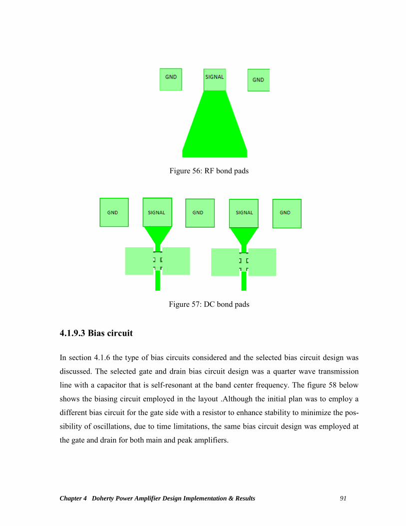
Chapter 4 Doherty Power Amplifier Design Implementation & Results 91
Figure 56: RF bond pads
Figure 57: DC bond pads
4.1.9.3 Bias circuit In section 4.1.6 the type of bias circuits considered and the selected bias circuit design was
discussed. The selected gate and drain bias circuit design was a quarter wave transmission
line with a capacitor that is self-resonant at the band center frequency. The figure 58 below
shows the biasing circuit employed in the layout .Although the initial plan was to employ a
different bias circuit for the gate side with a resistor to enhance stability to minimize the pos-
sibility of oscillations, due to time limitations, the same bias circuit design was employed at
the gate and drain for both main and peak amplifiers.

Chapter 4 Doherty Power Amplifier Design Implementation & Results 92
Figure 58: Layout design of bias circuit
4.1.9.4 Layout input and output matching networks In section 4.1.5.2 schematic components were used to realize the matching. Then the compo-
nents were replaced by layout foundry elements and additional transmission lines were in-
cluded to realize the layout. In order to null the ESR and ESL effects of the lumped elements
of the foundry and to take into account capacitances and inductances of the added distributed
elements, matching component values needed to be tuned to achieve the optimum impedanc-
es. Figure 60 and figure 61 depicts the schematic and layout designs of the matching net-
works. In reference to the following elements in figure 59, input matching components were
tuned as follows:
Figure 59: Tuned input matching equivalent circuit

Chapter 4 Doherty Power Amplifier Design Implementation & Results 93
Table 7: Input matching components before and after tuning
Component Original match
Tuned match
L1 0.4nH 0.8nH L2 n∕a 0.3nH L3 0.24nH 0.24nH C2 7.2pF 0.9pF C3 7.2pF 3.8pF
Output matching L and C values were changed as follows after tuning:
Table 8: Output matching components after and before tuning
Component Original match
Tuned match
L 2.6nH 3.6nH C 2.8pF 3.8pF
Following table summarizes the simulated verification results of the tuned layout match:
Table 9: Layout and schematic class AB performance summary
Parameter Class AB performance @
2.655GHz in schematic de-sign
Class AB performance @ 2.655GHz in layout design
Compressed Pout 39.7 dBm 40.23dBm Efficiency at compressed Pout 52.6% 49.98% Gain at compressed Pout 9dB 10dB

Chapter 4 Doherty Power Amplifier Design Implementation & Results 94
Figure 60: Schematic input and output matching networks
Figure 61: Layout input and output matching networks.

Chapter 4 Doherty Power Amplifier Design Implementation & Results 95
4.1.9.5 Doherty combiner layout In order to fit the full design in a 10mm x 11.5mm layout area, the Doherty combiner had to
be meandered as shown in figure 62 below:
Figure 62: Doherty combiner layout To verify the Doherty combiner design structure, a secondary set of impedances can be de-
fined as per figure 63 at nodes A, B and C with 50Ω load terminations.
If all three nodes (A, B and C) in figure 63 were terminated with 50Ohm, the impedances
looking into each node of the combiner would be:
A= 150Ω= (Zo2 / impedance 17 Ω at node B)
B = 17 Ω = (50 Ω parallel with 25 Ω)
C= 50 Ω
The simulated designed combiner impedances are reported in Figure 64.

Chapter 4 Doherty Power Amplifier Design Implementation & Results 96
Figure 63: Doherty combiner verification
Figure 64: Verification of layout design of the Doherty combiner As seen in figure 64, the designed combiner provides impedances close to the targeted im-
pedances at each node.

Chapter 4 Doherty Power Amplifier Design Implementation & Results 97
4.1.9.6 Complete Doherty amplifier layout Figure 65 below depicts the complete layout of the designed MMIC Doherty amplifier.
Figure 65: Layout of the designed MMIC Doherty amplifier

Chapter 4 Doherty Power Amplifier Design Implementation & Results 98
4.2 Doherty amplifier Performance Evaluation
This section of the report provides the single and dual tone simulation results of the designed
Doherty Power Amplifier. This segment also discusses various optimization methods to tune
the design for either optimum efficiency or linearity. Finally a literature study is presented to
compare the designed MMIC Doherty amplifier performance to previously published MMIC
amplifiers. The performance analysis of the designed Doherty topology was executed in co-
simulation of Agilent’s Advanced Design System 2009. B efore proceeding with the large
signal performance evaluation, a small-signal S-parameter characterization was performed on
the Doherty amplifier under a fixed drain bias of 20V and gate bias voltages of -3.0V and -
4.9V for the main and peaking amplifiers respectively.
The simulated small signal parameters S11 and S21 are shown in figure 66 below. It can be
observed that the Doherty amplifier provides a return loss of -14dB over the bandwidth of
2.62 to 2.69GHz.However, a frequency shift in the return loss can be observed. A flat small
signal gain of approximately 11.0dB has been measured over the frequency range of 2.62 to
2.69GHz.This accounts for the required bandwidth of the LTE band 7 base station applica-
tions.
4.2.1 Large signal single tone simulations
In order to assess the large-signal performance of the Doherty amplifier single-tone and two-
tone large signal simulations have been performed with a fixed drain bias of 20V. Figure 67
(a) and (c) show the single-tone power added efficiency response of the Doherty amplifier
along with that of a conventional class AB power amplifier. The figure clearly depicts that
the Doherty power amplifier has higher efficiency over a wider range of output power com-
pared to a Class AB power amplifier of the same power sizing. The key point to note is the
17% increase in efficiency at the back off power level of the Doherty power amplifier. Alt-
hough a relatively constant efficiency is expected in the full 6dB back off range, a slight dip
in the PAE between the two peak points can be noticed. This is due to the lower gain of the
peaking amplifier from Class C operation. This situation could be overcome by having an
unequal power division at the input, delivering higher power to the peaking amplifier than
the main amplifier [49].

Chapter 4 Doherty Power Amplifier Design Implementation & Results 99
Figure 66: Simulated small signal S-parameters of the Doherty Amplifier Figure 67 (b) shows the gain vs output power of the Doherty amplifier. Note the reduced gain
in Doherty mode in the upper 6dB range. This caused by the class C bias of the peaking am-
plifier. With this class C bias, it is typically difficult to match the gain of the full Doherty
amplifier to be greater than the main amplifier. Also note that, as per theory, the saturated
output power of the Doherty topology is approximately 6dB higher than the main amplifier
saturated output power which was shown in figure 48.
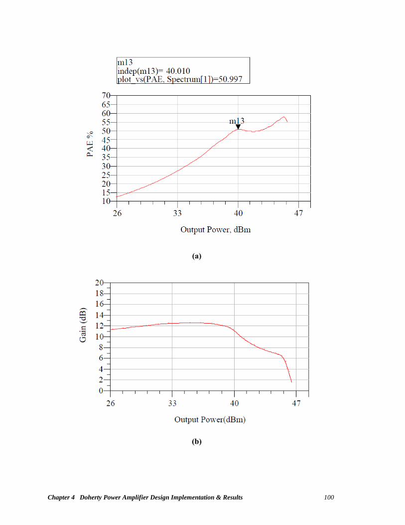
Chapter 4 Doherty Power Amplifier Design Implementation & Results 100
(a)
(b)

Chapter 4 Doherty Power Amplifier Design Implementation & Results 101
(c)
Figure 67: Single tone simulations with Vdrain=20V, Vgs_main=-3.0V,Vgs_peak=-4.9V (a) Power added efficiency of the Doherty amplifier (b) Gain of the Doherty amplifier (c) Com-
parison of Power added efficiencies of Class AB and Doherty amplifiers
4.2.2 Large signal two tone simulations
Two tone simulations were performed to qualitatively analyze the linearity of the Doherty
amplifier. Figure 68 shows the simulated third and fifth order intermodulation products
(IMD3 and IMD5) of the Doherty amplifier at its nominal bias points for main and peaking
amplifiers (Vdrain=20V, Vgs_main=-3.0V, Vgs_peak=-4.9V) at 2.655GHz with tone spac-
ing of 1MHz. Due to the distortion caused by the low biasing of the peaking amplifier the
intermodulation distortion of the Doherty amplifier looks to be poor. By altering the bias
conditions of the peaking amplifier, proper turn on c haracteristics can be achieved to sup-
press these distortion levels. This would be further discussed during Doherty topology opti-
mization in section 4.2.4. Also, since the base station power amplifiers are typically operated
with a linearization system, the observed IMD levels should be sufficient for a base station
application.
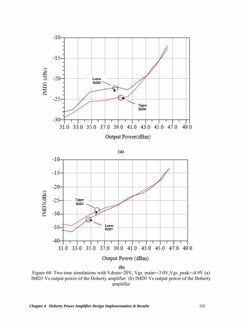
Chapter 4 Doherty Power Amplifier Design Implementation & Results 102
(a)
(b)
Figure 68: Two tone simulations with Vdrain=20V, Vgs_main=-3.0V,Vgs_peak=-4.9V (a) IMD3 Vs output power of the Doherty amplifier (b) IMD5 Vs output power of the Doherty
amplifier

Chapter 4 Doherty Power Amplifier Design Implementation & Results 103
4.2.3 Thermal dissipation
Following Table 10 shows the current draw and the thermal dissipation of the designed
Doherty MMIC.
Table 10: Thermal dissipation and total current draw of the Doherty PA
As seen by the data in the table, the thermal dissipation for this design is quite low. When
working with GaN it is critical to pay attention to thermal dissipation. While the RF power
densities of GaN scale up to values of 30 w/mm unit-gate width but quantities such as ther-
mal conductivities of the substrate and packaging materials, maximum system temperatures,
and allowable dissipated power per area do not scale accordingly. Therefore, thermal man-
agement is crucial in order to utilize at least a fraction of the maximum potential of GaN in
packaged devices and mounted MMICs . A commercial GaN vendor Cree states the follow-
ing “Reports of high total RF power from both SiC and GaN over a wide frequency range are
beginning to validate the very high power densities that have been demonstrated on s mall
periphery devices for several years. These high power densities in terms of W/mm also pre-
sent an extreme power dissipation demand on t he substrate. Fortunately, the high thermal
conductivity of the SiC substrates, >3.3 W/cm-K, allows these higher power densities to be
efficiently dissipated, preventing the extreme channel temperatures due to self-heating that
are likely with low thermal conductivity substrates such as sapphire and silicon.” [54].
Chapter 4 Doherty Power Amplifier Design Implementation & Results 104
There are number of methods that can be implemented to ease this high thermal dissipation
such as flip-chip mounting, cluster matching (a way of distributing the signal among a num-
ber of smaller devices in order to spread the head over a wider area) and bath-tub via pro-
cessing (substrate is thinned only under the power devices since a thinner substrate would
provide good heat dissipation).
4.2.4 Performance Optimization
In this section of the report, performance optimization of the Doherty amplifier is executed
by altering the biasing of the main and peaking amplifier. An analysis of the impact of vari-
ous biasing on the main and peaking amplifier of the Doherty amplifier is discussed showing
the trade-offs between gain and efficiency of the full Doherty amplifier. The choice of opera-
tion of the amplifier depends mainly on the requirement of the application; therefore a suita-
ble biasing scheme needs to be selected depending on the application.
4.2.4.1 Main and peaking amplifier bias optimization This section discusses the impact on the full Doherty amplifier with various biasing of the
main and peaking stages of the amplifier. As the primary intent of the Doherty technique is
to provide high efficiency, the common approach is to bias the main amplifier for class AB
or B operation .In this optimization step, the peaking amplifier was biased at a constant class
C (Vgs= -4.9V) and the main amplifier gate voltage was adjusted from -0.5V to -3.5V to
vary the class of operation from class A to deep class AB to class AB. Figure 69 summarizes
the outcome of this experiment.
By observing Figure 69 (a), it can be seen that there is a drop in efficiency, as the gate volt-
age is increased closer to class A operation of the main amplifier. The effect of the increased
gate voltage can be seen especially at the back off power level. The gain response of the am-
plifier in Figure 69 (b) indicates a reduction in gain with reduced bias of the main amplifier.

Chapter 4 Doherty Power Amplifier Design Implementation & Results 105
(a)
(b)
Figure 69: Doherty amplifier optimization with main amplifier bias variation (a) PAE re-sponse of Doherty amplifier with variation in main amplifier bias (b) Gain response of Doherty amplifier with variation in main amplifier bias
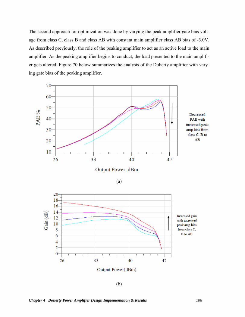
Chapter 4 Doherty Power Amplifier Design Implementation & Results 106
The second approach for optimization was done by varying the peak amplifier gate bias volt-
age from class C, class B and class AB with constant main amplifier class AB bias of -3.0V.
As described previously, the role of the peaking amplifier to act as an active load to the main
amplifier. As the peaking amplifier begins to conduct, the load presented to the main amplifi-
er gets altered. Figure 70 below summarizes the analysis of the Doherty amplifier with vary-
ing gate bias of the peaking amplifier.
(a)
(b)

Chapter 4 Doherty Power Amplifier Design Implementation & Results 107
(c)
Figure 70: Doherty amplifier optimization with peaking stage bias variation (a) PAE re-sponse of Doherty amplifier with variation in peaking amplifier bias (b) Gain of the Doherty amplifier with variation in peaking amplifier bias (c) IMD3 response of Doherty amplifier
By observing the PAE response in figure 70 (a), the corresponding reduction in the back off
efficiency can be observed with Class B and AB bias of the peaking amplifier. The maximum
efficiency at back off reached when the peaking amplifier is biased in class C. Figure 70
(b),exhibits that maximum output power can be varied with variation in gain by adjusting the
class of peaking amplifier bias. There is also degradation in linearity with peaking amplifier
bias closer to class C mode which is indicated by the IMD3 plots in figure 70(c). With the
above results, the following can be concluded:
• When main amplifier is biased higher, the overall gain of the Doherty amplifier re-
duced.
• When peaking amplifier is operated at higher bias levels, the overall Doherty amplifi-
er exhibits better linearity with higher gain but reduces the back off efficiency of the
Doherty amplifier as a result of reduced load modulation range.
• When peaking amplifier is operated at lower bias levels as class C, efficiency at back
off is increased but with reduced linearity.

Chapter 4 Doherty Power Amplifier Design Implementation & Results 108
Thus, the operating point of the Doherty amplifier has to be decided based on t he system
considerations of the full base station to decide the proper trade-offs between efficiency and
linearity. For instance if the power amplifier is intended to be implemented with a lineariza-
tion technique as digital pre distortion, more emphasis can be placed on the efficiency aspect
of linearization.
4.2.5 Full LTE band-7 over frequency performance summary
A summary of full LTE band-7 over frequency performance of the designed MMIC Doherty
Amplifier is given in Table 11.
Table 11: Full LTE band-7 performance summary of the MMIC Doherty Amplifier
Parameter 2.62 GHz 2.655GHz 2.69GHz Gain (dB) 11.19 11.10 11.09
PAE at back off power (%) 51.29% 51.09% 50.52%
PAE at peak power (%) 53.31% 56.27% 59.89%
IMD3 (dBc) -19.95 -20.2 -21.45
(a)

Chapter 4 Doherty Power Amplifier Design Implementation & Results 109
(b)
Figure 71: Simulated over Frequency performance of the Doherty Amplifier with Vdrain=20V, Vgs_main=-3.0V,Vgs_peak=-4.9V (a) Over frequency PAE % of the designed
MMIC Doherty Amplifier

Chapter 4 Doherty Power Amplifier Design Implementation & Results 110
The designed MMIC Doherty amplifier performance can be compared to published MMIC
amplifier performances as follows:
Table 12: Performance comparison of the designed Doherty PA to published MMIC PAs.
Ref Year published
Frequency (GHz)
Device Technology
Peak power (W)
PAE at peak power (%)
PAE at back off
power (%)
This thesis 2.65 GaN 40 56.3% 3 51.1% 3
[69] 2011 3.5 GaN 31 45% 2 15% 2
[70] 2010 7.0 GaN 2.5 51% 3 31% 3
[71] 2010 2.6 GaAs 0.5 34% 1 23% 1
[72] 2009 2.0 GaN 2 35% 18%
[73] 2009 2.0 GaN 10 42.2 % 33%
[74] 2008 3.1 GaN 38 37% 2 18% 2
[75] 2008 3.0 GaN 5 32.5 % 18 %
[76] 2008 4.0 GaN 10 45 % 35%
[77] 2006 1.9GHz GaAs 1 38% 1 35% 1
1 Measured Doherty results 2 Simulated results with other architectures 3 Simulated Doherty results
Chapter 5 Conclusion and Future Work 111
Chapter 5 Conclusion and Future Work
5.1 Summary
In this research efficiency enhancement of a GaN based power amplifier is explored. This is
implemented through the design of a MMIC two-way Doherty power amplifier for a pico-
cell base station that would meet requirements of LTE standards. The intent was to realize a
Doherty topology suitable for a base station by improving its characteristics compared to ex-
isting conventional power amplifiers and other efficiency enhancement techniques while
meeting the stringent form factor requirements of a pico-cell. Demonstrative design and im-
plementation have been provided based on t he emerging GaN device technology. Specific
advantages of GaN such as low output capacitance, high output impedance and higher power
density have been utilized at various stages of the thesis.
During this research, the most common conventional PAs such as class A, B, AB and C were
reviewed. An overview of currently available power amplifier efficiency enhancing methods
such as Envelope Elimination and restoration, Envelope tracking and Chireix Outphasing is
also presented. A detailed discussion on t he theory of the Doherty topology was provided
along with an overview of GaN semiconductor technology. It is illustrated how a GaN based
Doherty architecture is the optimum selection for the application considered.
The Doherty amplifier design approach presented in this dissertation relies on reliable accu-
rate CAD tools for analysis and optimization. Therefore in order to assess the accuracy and
reliability of large-signal models for a new device technology as GaN, experiments were per-
formed on a commercial GaN design to validate the large-signal models by comparing the
measured and simulated behavior of a printed circuit board (PCB) based class AB GaN pow-
er amplifier design.
Based on the Doherty concept, a design of a MMIC power amplifier was implemented for
LTE band 7 which entails the frequency band from 2.62-2.69GHz. . The design was simulat-
ed and the results were compared with that of the theoretical Doherty amplifier as well as a

Chapter 5 Conclusion and Future Work 112
corresponding conventional class AB power amplifier. The full layout of the design is pre-
sented comprising the conversion of the schematic design into something that is able to be
fabricated by the foundry. The impact of the main and peaking stage biasing on the overall
performance was also analyzed and options to optimize linearity with the least amount of re-
duction in the improved efficiency is presented to cater various system requirements.
5.2 Conclusion
The MMIC Doherty amplifier design, reported in this thesis has demonstrated the feasibility
of achieving high efficiency at the back off power levels while maintaining reasonable linear-
ity compared to conventional PA designs. Although the linearity reported in this design does
not directly satisfy LTE requirements, additional linearization can be applied to achieve the
required correction. It is essential to note the efficiency achieved in this thesis is the highest
at back off power levels compared to published MMIC PA designs. The most significant
contribution of this thesis is the detailed design and implementation of a two way MMIC
Doherty amplifier for LTE standards that is applicable for a pico-cell base station. It demon-
strates a PAE of 50.5% in the 6dB back off power from a peak power of 46dBm, for the full
LTE band 7 which entails the frequency band from 2.62-2.69GHz.Additional contribution is
offered through the bias optimization technique presented for the main and peaking amplifi-
ers to shift between a highly linear or highly efficient performance of the same design.
5.3 Future Work
Improving efficiency of power amplifiers at high back off levels while sustaining linearity
will remain an essential aspect of future work. With the growing trend towards the usage of
pico-cell base stations, fully integrated MMIC designs of power amplifiers will also gain
more traction. 4G standards as LTE could utilize signals with PAPRs up to 10dB with broad
instantaneous bandwidths (IBWs) of up to 60MHz.The following recommendations can be
considered to further expand the direction of research:
• MMIC Doherty amplifier presented in this thesis can be further analyzed by imple-
menting a linearization technique such as digital pre-distortion. This would add fur-

Chapter 5 Conclusion and Future Work 113
ther value to the design by retrieving the degraded linearity that was compromised for
higher efficiency.
• In order to support PAPRs of higher than 6dB, the back-off region can be extended by
implementing the MMIC design in an asymmetrical or a multi-stage Doherty archi-
tecture. An asymmetric topology would consist of main and peaking amplifiers of dif-
ferent sizing and N-stage design would consist of multiple peaking amplifiers.
• In order to support higher IBWs, the MMIC Doherty amplifier design can be further
optimized to have broad video bandwidths. Implementation of multi section λ∕4 bias
feeds, multiple radial stubs and addition of selected decoupling capacitors with reso-
nance frequencies distributed over the entire video bandwidth are a few methods that
can be implemented.

114
References
[1] Wikipedia (2012). "Picocell". Retrieved from http://en.wikipedia.org/wiki/Picocell.
[2] BelAir Networks (2011). "BelAir networks new small cell base station combines LTE
and Wi-Fi to address ongoing mobile data demand". Retrieved from
http://www.belairnetworks.com/news/press-releases/belair-networks-new-small-cell-
base-station-combines-lte-and-wi-fi-address
[3] M. Steer, “Beyond 3G,” IEEE Microwave Magazine, IEEE, 2007, Vol. 8, pp. 76-82
[4] M. Feng, S. Shyh-Chiang, D.C. Caruth, J.-J. Huang, “Device technologies for RF front-
end circuits in next-generation wireless communications,” Proc. IEEE, 2004, Vol. 92,
pp. 354-375
[5] F.H. Raab, P. Asbeck, S. Cripps, P.B. Kenington, Z.B. Popovic, N. Pothecary, J.F. Se-
vic, N.O. Sokal, “Power amplifiers and transmitters for RF and microwave,” IEEE
Trans. Microwave Theory Tech., 2002, Vol. 50, pp. 814-826
[6] 3GPP-LTE (2012). "LTE keywords and acronyms". Retrieved from
http://www.3gpp.org/LTE
[7] S. Sesia, I. Toufik, M. Baker, LTE-The UMTS long term evolution-from theory to
practice, John Wiley & Sons, 2011
[8] M.K. Nezami, “Feedforward power amplifier linearization for 4G base station,” IEEE
9th Malaysia Int. Conf. on Communications, 2009, pp. 880-884.
[9] A.M.A. Hemmatyar, F. Farzaneh, “Estimation of practical inter-modulation rejection
values in a multi-loop feed-forward microwave power amplifier using Monte-Carlo
method,” Sharif Univ. of Technol., Tehran, 2007, pp. 632-637.
[10] K.K. Mohammed, R.B. Mohammed, “Linearization of power amplifier class AB using
Cartesian feedback,” Int. Multi-Conf. on Systems Signals and Devices, 2010, pp. 1-6.
[11] J.L. Dawson, T.H. Lee, “Cartesian feedback for RF power amplifier linearization,”
American Control Conf., 2004
115
[12] P. Garcia, A. Ortega, J. de Mingo, A. Valdovinos, “Nonlinear distortion cancellation in
OFDM systems using an adaptive LINC structure,” 15th IEEE Int. Symp. on Personal,
Indoor and Mobile Radio Communications, 2004, pp. 1506-1510.
[13] R. Sperlich, J.A. Sills, J.S. Kenney, “Power amplifier linearization with memory effects
using digital pre-distortion and genetic algorithms,” Radio and Wireless Conf., 2004,
pp. 355-358
[14] R. Sperlich, Y. Park, G. Copeland, J.S. Kenney, “Power amplifier linearization with
digital pre-distortion and crest factor reduction,” IEEE MTT-S Int. Microwave Symp.,
2004, pp. 669-672
[15] J.A. Sills, R. Sperlich, “Adaptive power amplifier linearization by digital pre-distortion
using genetic algorithms,” Radio and Wireless Conf., 2002, pp. 229-232
[16] J. Vuolevi, T. Rahkonen, J. Manninen, “Measurement technique for characterizing
memory effects in RF power amplifiers,” Meeting Dept. of Electr. Eng., Oulu Univ.,
pp. 195 – 198, 2000.
[17] S.C. Cripps, RF Power Amplifers for Wireless Communications. Norwood, MA: Ar-
tech House, 1999.
[18] H.H. Ladhani, J.K. Jones, G. Bouisse, “Improvements in the instantaneous-bandwidth
capability of RF Power Transistors using in-package high-k capacitors,” IEEE MTT-S
Int. Microwave Symp., 2011, pp. 1-4
[19] A.Z. Markos, “Efficiency enhancement of linear GaN RF power amplifiers using the
Doherty technique,” University of Kassel, Germany, 2008
[20] B. Kopp, D.D. Heston, “High-efficiency 5-watt power amplifier with harmonic tun-
ing,” IEEE MTT-S Int. Microwave Symp., 1988, pp. 839-842
[21] R. Meshkin, A. Saberkari, M. Niaboli-Guilani, “A novel 2.4 GHz CMOS class-E pow-
er amplifier with efficient power control for wireless communications,” 17th IEEE Int.
Conf. on Electronics, Circuits, and Systems, 2010, pp. 599-602
[22] H. Chireix, “High power outphasing modulation,” Proc. IRE, Vol. 23, pp. 1370-1392,
1935.
[23] W. Gerhard, R. Knoechel, “Improvement of power amplifier efficiency by reactive
Chireix combining, power back-off and differential phase adjustment,” IEEE MTT-S
Int. Microwave Symp., 2006, pp. 1887-1890
116
[24] E. Napieralska, M. Zannoth, G. Kraut, W. Bakalski, E. Biebl, K. Kitlinski, Q. Neubib-
erg, “Outphasing power amplifier design investigations for 2.5G and 3G standards,”
European Microwave Conf., 2007, pp. 1181-1184
[25] S. Hong, Y.Y. Woo, I. Kim, J. Kim, J. Moon, H.S. Kim, J.S. Lee, B. Kim, “High effi-
ciency GaN HEMT power amplifier optimized for OFDM EER transmitter,” IEEE
MTT-S Int. Microwave Symp., 2007, pp. 1247-1250
[26] L.R. Kahn, “Single-sideband transmission by envelope elimination and restoration,”
Proc. IRE, Vol. 40, 1952, pp. 803-806.
[27] F.H. Raab, E.B. Sigmon, G.R. Myers, M.R. Jackson, “L-band transmitter using Kahn
EER technique,” IEEE Trans. Microwave Theory Tech., 1998, Vol. 46, pp. 2220-2225.
[28] W.H. Doherty, “A new high efficiency power amplifier for modulated waves,” Proc.
IRE, Vol. 24, 1936, pp-1163-1182
[29] H. Harju, T. Rautio, S. Hietakangas, T. Rahkonen, “Envelope tracking power ampli-
fier with static predistortion linearization,” 18th European Conf. on Circuit Theory and
Design, 2007, pp. 388-391
[30] Nitronex, AN-011: Substrates for GaN RF Devices, Nitronex Corporation, 2008.
[31] I. Rosu, “RF Power Amplifiers”. Retrieved from http://www.qsl.net/va3iul
[32] V. Viswanathan, “Efficiency enhancement of base station power amplifiers using
Doherty technique,” M.A.Sc thesis, Virginia Polytechnic Institute and State University,
2004
[33] M. Feng, S. Shyh-Chiang, D.C. Caruth, J.-J. Huang, “Device technologies for RF front-
end circuits in next-generation wireless communications,” Proceedings of the IEEE,
Feb 2004, Vol. 92, pp. 354 - 375
[34] N. Le Gallou, J.M. Nebus, E. Ngoya, H. Buret, “Analysis of low frequency memory
and influence on s olid state HPA intermodulation characteristics,” IEEE MTT-S Int.
Microwave Symp., 2001, pp. 979-982.
[35] T. Nesimoglu, “Linearity and efficiency performance of a modified envelope elimina-
tion and restoration transmitter architecture,” East Technical University, Turkey.
[36] F. Wang, A.H. Yang, D.F. Kimball , L.E. Larson, PM. Asbeck, “Design of wide-
bandwidth envelope-tracking power amplifiers for OFDM applications” IEEE Trans.
Microwave Theory Tech., Vol. 53, 2005.
117
[37] I. Hakala1, L. Gharavi, R. Kaunisto, “Chireix power combining with saturated class-B
power amplifiers” 12th GaAs Symp., pp 379-382, 2004
[38] F.H. Raab, “Efficiency of outphasing RF power amplifer systems,” IEEE Trans. Com-
mun., Vol. 33, pp. 1094-1099, 1985.
[39] A. Grebennikovic, “A_High-efficiency 100-W four-stage Doherty GaN HEMT power
amplifier module for WCDMA systems,” Bell Labs, Alcatel-Lucent, Ireland, 2011.
[40] M.J. Pelk, W.C. Edmund Neo, J.R. Gajadharsing, R.S. Pengelly, L.C.N. de Vreede. “A
high-efficiency 100-W GaN three-way Doherty,” IEEE MTT-S Int. Microwave Symp.,
2008.
[41] Y. Yang, J. Cha, B. Shin, B. Kim, “Optimum design for linearity and efficiency of a
microwave Doherty amplifier using a new load matching technique,” Microwave J.,
2003.
[42] R. Darraji, F.M. Ghannouchi, O. Hammi, “A dual-input digitally driven Doherty am-
plifier architecture for performance enhancement of Doherty transmitters,” IEEE Trans.
Microwave Theory Tech., 2011, Vol. 59, pp. 1284-1293
[43] S. Chalermwisutkul, “Large signal modeling of GaN HEMTs for UMTS base station
power amplifier design taking into account memory effects,” Aachen University, 2007.
[44] C.E. Weitzel, “RF power devices for wireless communications,” IEEE RFIC Symp.,
2002, pp.369-372.
[45] C.E. Weitzel, “ RF power amplifers for wireless communications,” 2002 IEEE GaAs
Symp., pp 127-130
[46] R.S Pengelly “Improving the linearity and Efficiency of RF power amplifiers,” High
Frequency Electronics, 2002,Vo. l1, pp 26-34
[47] R. Borges, “Gallium nitride electronic devices for high power wireless applications”
RF design, 2001, pp-72-82
[48] I.I. Blednov, J. Van Der Zanden, “High power LDMOS integrated Doherty amplifier
for W-CDMA,” IEEE Radio Frequency Integrated Circuits Symp., 2006.
[49] D. Kang, J. Choi, D. Kim, D. Yu, K. Min, B. Kim, “30.3% PAE HBT Doherty power
amplifier for 2.5∼2.7 GHz mobile WiMAX,” IEEE MTT-S Int. Microwave Symp.,
2010, pp. 796-799.
[50] J.M Golio, RF and microwave semiconductor device handbook, CRC Press, 2003

118
[51] S.C. Binari, K. Ikossi, J.A. Roussos, W. Kruppa, D. Park, H.B. Dietrich, D.D. Koleske,
A.E. Wickenden, R.L. Henry, “Trapping effects and microwave power performance in
AlGaN/GaN HEMTs,” IEEE Trans. Elect. Devices, Vol. 48, 2001.
[52] S. Chalermwisutkul, “Large signal modeling of GaN HEMTs for UMTS base station
power amplifier design taking into account memory effects,” Aachen University, 2007.
[53] D. Pavlidis, P. Valizadeh, S.H. Hsu, “AlGaN/GaN high electron mobility transistor
(HEMT) reliability” 13th GAAS Symp., 2005, pp. 265-268
[54] Cree, Inc. (2012) “CGH25120F Datasheet”. Retrieved from
http://www.cree.com/products/pdf/CGH25120F.pdf
[55] J. Moon, Y.Y. Woo, B. Kim, “A Highly efficient Doherty power amplifier employing
optimized carrier cell,” Pohang University of Science and Technology, Gyeongbuk,
Republic of Korea.
[56] F.H. Raab, “Efficiency of Doherty RF Power-amplifier systems,” IEEE Transactions
On Broadcasting, Vol. Bc-33, No. 3, September 1987.
[57] J. Brinkhoff, A.E. Parker, “Effect of baseband impedance on FET intermodulation,”
IEEE Trans. Microwave Theory Tech., Vol. 51, 2003, pp. 1045-1051.
[58] N. Borges de Carvalho, J.C. Pedro, “A comprehensive explanation of distortion side-
band asymmetries,” IEEE Trans. Microwave Theory Tech., Vol. 50, 2002, pp. 2090-
2101.
[59] L. Pelletier. (2010). “Doherty amps and the three amigos”. Retrieved from
http://www.eetimes.com/design/industrial-control/4019101/Doherty-Amps-and-the-
Three-Amigos
[60] J.H. Qureshi, L. Nan, E. Neo, F.V. Rijs, I. Blednov, L. de Vreede, “A wide-band 20W
LDMOS Doherty power amplifier,” IEEE MTT-S Int. Microwave Symp., 2010
[61] R.J. Trew, “Wide band-gap semiconductor transistors for microwave power amplifi-
ers,” IEEE Microwave Magazine, 2000, Vol. 1, pp. 46-54
[62] G. Norris, et al., “Application of digital adaptive pre-distortion to mobile wireless de-
vices,” IEEE RFIC Symp., 2007, pp. 247-250.
[63] A. Afsahi, et al., “Fully integrated dual-band power amplifiers with on-chip baluns in
65nm CMOS for an 802.11n MIMO WLAN SoC’’, IEEE RFIC Symp., 2009, pp. 368-
365.

119
[65] M. Venkataramani, “Efficiency improvement of WCDMA base station transmitters us-
ing Class-F power amplifiers,” University of Virginia, 2004.
[66] J.F. Sevic, J. Staudinger, “Simulation of power amplifier adjacent-channel power ratio
for digital wireless communication systems,” IEEE 47th Vehicular Technology Conf.,
1997, pp. 681-685.
[67] H.L. Krauss, C.W. Bostain, F.H. Raab, Solid State Radio Engineering. New York, NY:
John Wiley & Sons, 1980.
[68] U.K. Mishra, P. Parikh, Y.-F. Wu, “AlGaN/GaN HEMTs-An overview of device oper-
ation and applications,” Proc. IEEE, Vol. 90, 2002.
[69] O. Cengiz, O. Kelekçi1, G.O Arıcan, E. Özbay, O. Palamutçuoğulları, “Design of High
Power S-Band GaN MMIC Power Amplifiers for WiMAX Applications,” IEEE Gen-
eral Assembly and Scientific Symp., 2011, pp.1-4
[70] R. Quaglia, , V. Camarchia, M. Pirola, S. Donati Guerrieri , “7 GHz GaN MMIC Pow-
er Amplifier for Microwave Radio links with 45% Drain Efficiency in a Wide Power
Range,” IEEE Integrated Nonlinear Microwave and Millimeter-Wave Circuits
(INMMIC) Conf., 2010, pp. 160 - 163
[71] D.Kang, J.Choi, D.Kim, D.Yu, K.Min, B.Kim, “30.3% PAE HBT Doherty Power Am-
plifier for 2.5-2.7 GHz Mobile WiMAX,” IEEE Microwave Symposium Digest (MTT)
Conf., 2010., pp. 796 – 799.
[72] K.W. Kobayashi, Y.C Chen, I. Smorchkov , B. Heying, W. Luo, M. Wojtowicz, A.Oki
, “A Cool, Sub-0.2 Db Noise Figure Gan Hemt Power Amplifier With 2-Watt Output
Power ” IEEE Solid-State Circuits J., Vol. 44, No. 10, 2009, pp.2648-2654
[73] K. Krishnamurthy, D. Green, R. Vetury, M. Poulton, J. Martin, “0.5–2.5 GHz, 10W
MMIC Power Amplifier in GaN HEMT Technology,” IEEE Compound Semiconduc-
tor Integrated Circuit Symp., 2009, pp.1-4
[74] M.V Heijningen, J. Würfl , G.C. Visser , F.E. van Vliet, “S-Band AlGaN/GaN Power
Amplifier MMIC with over 20 Watt Output Power,” IEEE European Microwave Inte-
grated Circuits Conf.,2008, pp. 79-82.
[75] E.M Sujiker, M.Sudow, M.Fagerlind, N.Rorsman, F.E Vanvliet , “GaN MMIC Power
Amplifiers for S-band and Xband , ” IEEE European Microwave Conf., 2008, pp. 297-
300

120
[76] M.A Gonzalez, J. Grajal, P. Cubilla, A. Cetronio , “2-6 GHz GaN MMIC power ampli-
fiers for electronic warfare applications,” IEEE European Microwave Integrated Cir-
cuits Conf, 2008, pp. 83-86
[77] T.Kato, K. Yamaguchi, Y. Kuriyama, “A Doherty power amplifier module for mobile
terminals with variable linearity function,” IEEE Asia-Pacific Microwave Conf., 2006,
pp. 1881 - 1884
[78] National Research Council Canada Canadian Photonics Fabrication Centre “NRC-
CPFC Gallium Nitride MMIC Foundry Design Manual, GaN500 Version 1.0” Revi-
sion date: January 27, 2011
[79] A.Dow, “Evolution to Femto cells for Radio access,” Alcatel-Lucent, 2008
[80] H.Tarn, E.Hemphill, D. Hawke, “3GPP LTE digital front end reference design,” Xil-
inx, XAPP1123, 2008.
[81] Y.Li , R .Zhu, D. Prikhodko,Y.Tkachenko, “LTE power amplifier module design: challenges
and trends,” Skyworks Solutions, 2010.
[82] H.D Bui, “A Doherty power amplifier with collector current and voltage controls”,
M.S.Eng Thesis, University of Massachusetts – Lowell, 2008.
[83] J. Gajadharsing, “3 Way Doherty amplifier design”, NXP, 2011.
[84] J.Brown (2011). “Will LTE Picocells and Wi-Fi Steal Femtocells Momentum?”, Re-
trieved from http://jackbrowntelecomprofessional.wordpress.com/2011/08/04/will-lte-
picocells-and-wi-fi-steal-femtocells-momentum/
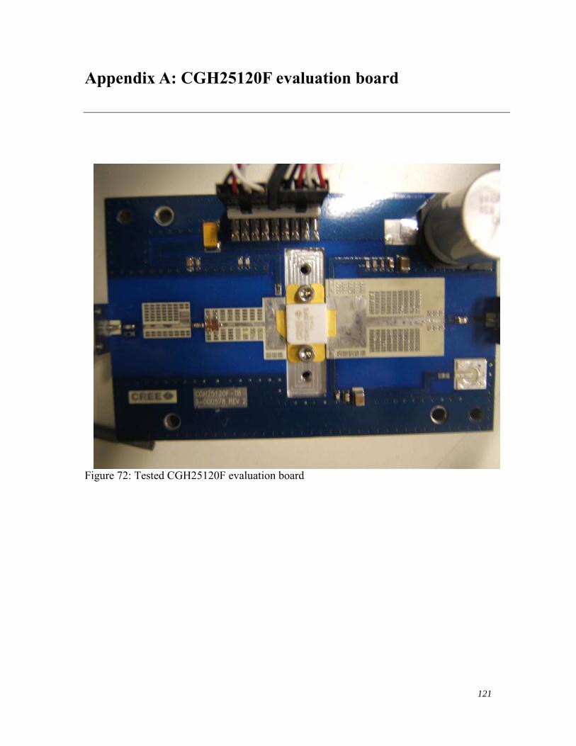
121
Appendix A: CGH25120F evaluation board
Figure 72: Tested CGH25120F evaluation board

122
Figure 73: Datasheet image of CGH25120F evaluation board [54]
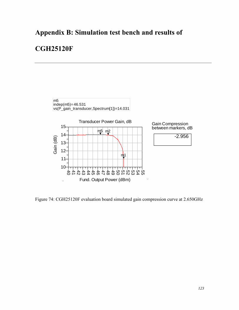
123
Appendix B: Simulation test bench and results of
CGH25120F
-2.956
41 42 43 44 45 46 47 48 49 50 51 52 53 5440 55
11
12
13
14
10
15
Fund. Output Power (dBm)
G
ain
(dB
)
m2
m1
m5
Transducer Power Gain, dB
m5indep(m5)=vs(P_gain_transducer,Spectrum[1])=14.031
46.531
Gain Compressionbetween markers, dB
Figure 74: CGH25120F evaluation board simulated gain compression curve at 2.650GHz
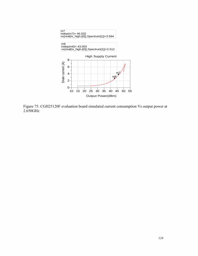
124
15 20 25 30 35 40 45 5010 55
2
4
6
0
8
Output Power(dBm)
D
rain
curre
nt (A
)
m6m7
High Supply Current
m6indep(m6)=vs(real(Is_high.i[0]),Spectrum[1])=2.512
43.003
m7indep(m7)=vs(real(Is_high.i[0]),Spectrum[1])=3.594
46.032
Figure 75: CGH25120F evaluation board simulated current consumption Vs output power at 2.650GHz
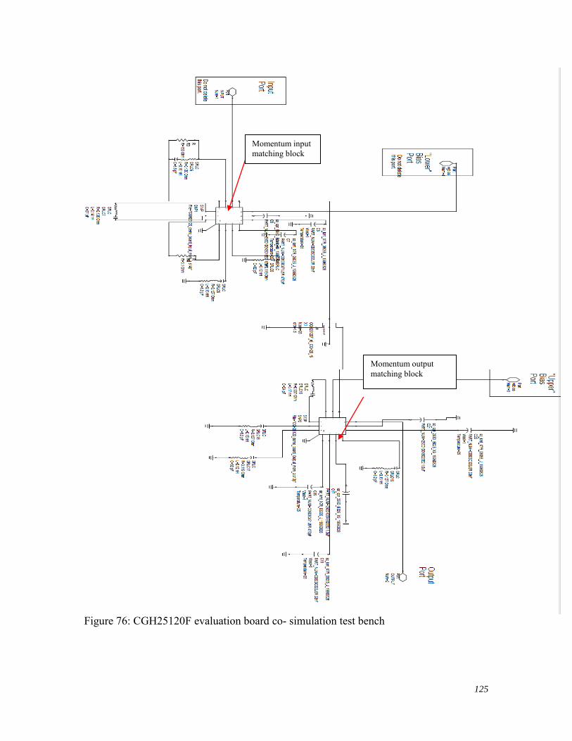
125
Figure 76: CGH25120F evaluation board co- simulation test bench
Momentum input matching block
Momentum output matching block

126
Appendix C: Measurement setup for CGH25120F
Figure 77: Measurement setup for CGH25120F