Embed Size (px)
Citation preview
EFFICIENCY ENHANCEMENT OF BASE STATION POWER AMPLIFIERS USING DOHERTY TECHNIQUE
Vani Viswanathan
Thesis submitted to the faculty of the
Virginia Polytechnic Institute and State University
in partial fulfillment of the requirements for the degree of
Master of Science
In
Electrical Engineering
Charles W. Bostian, Chair
Sanjay Raman
Alex Q. Huang
February 3, 2004
Blacksburg, Virginia
Keywords: Doherty power amplifier, LDMOS,
WCDMA, efficiency enhancement
Copyright 2004, Vani Viswanathan
EFFICIENCY ENHANCEMENT OF BASE STATION POWER
AMPLIFIERS USING DOHERTY TECHNIQUE
By
Vani Viswanathan
ABSTRACT The power amplifiers are typically the most power-consuming block in wireless communication
systems. Spectrum is expensive, and newer technologies demand transmission of maximum
amount of data with minimum spectrum usage. This requires sophisticated modulation
techniques, leading to wide, dynamic signals that require linear amplification. Although linear
amplification is achievable, it always comes at the expense of efficiency. Most of the modern
wireless applications such as WCDMA use non-constant envelope modulation techniques with a
high peak to average ratio. Linearity being a critical issue, power amplifiers implemented in such
applications are forced to operate at a backed off region from saturation. Therefore, in order to
overcome the battery lifetime limitation, a design of a high efficiency power amplifier that can
maintain the efficiency for a wider range of radio frequency input signal is the obvious solution.
A new technique that improves the drain efficiency of a linear power amplifier such as Class A
or AB, for a wider range of output power, has been investigated in this research. The Doherty
technique consists of two amplifiers in parallel; in such a way that the combination enhances the
power added efficiency of the main amplifier at 6dB back off from the maximum output power.

The classes of operation of power amplifier (A, AB,B, C etc), and the design techniques are
presented. Design of a 2.14 GHz Doherty power amplifier has been provided in chapter 4. This
technique shows a 15% increase in power added efficiency at 6 dB back off from the
compression point. This PA can be implemented in WCDMA base station transmitter.
iii

Acknowledgements I wish to express my most sincere gratitude and appreciation to my advisor, Dr. Charles W. Bostian,
for an outstanding experience here at Virginia Tech. It has been a great experience working with
him, and the lessons I have learned will stay with me throughout my career. I would like to thank
him for the constant inspiration and encouragement throughout my Masters program.
I would also like to thank my committee members Dr. Sanjay Raman and Dr. Alex Q.Huang for
their review of my thesis and helpful comments. Special thanks to Dr. Cedric Cassan and
Mr. Robert Kesseler of Motorola for help with the ADS design kits and reference materials.
I wish to acknowledge and give my appreciation to all the people of the Center for Wireless
Telecommunications, Virginia Tech, without whom, this work as it stands, would not have been
possible.
Lastly, I would like to thank my parents, Viswanathan and Shobhana and my sister, Vidhya for their
patience, support, guidance and acceptance of my endeavors.
iv

Table of Contents
Abstract…………………………………………………………………………. ii
Acknowledgements……………………………………………………………... iv
Table of Contents………………………………………………………………. v
List of Figures…………………………………………………………………... viii
List of Tables……………………………………………………………………. xi
Glossary of Acronyms………………………………………………………….. xii
1 INTRODUCTION…………………………………………………………… 1
1.1 Background……………………………………………………………….. 1
1.2 Research Goals…………………………………………………………… 2
1.3 Report Organization………………………………………………………. 3
2 RF POWER AMPLIFIERS…………………………………………………. 4
2.1 Classes of PA operation…………………………………………………… 4
2.1.1 Class A………………………………………………………………. 5
2.1.2 Class B………………………………………………………………. 6
2.1.3 Class AB…………………………………………………………….. 7
2.1.4 Class C………………………………………………………………. 8
2.2 Characteristics of power amplifiers……………………………………….. 8
2.2.1 Linearity…………………………………………………………….. 8
2.2.2 Measurement of Linearity…………………………………………… 8
2.2.2.1 1 dB Compression point…………………………………… 9
2.2.2.2 Intermodulation Distortion………………………………….. 10
2.2.2.3 Third order Intercept point………………………………….. 11
2.2.3 Efficiency…………………………………………………………… 12
v

2.2.4 Noise………………………………………………………………… 12
2.3 LDMOS Power Transistors………………………………………………... 13
2.4 Conclusion…………………………………………………………………. 14
3 DOHERTY POWER AMPLIFIERS………………………………………... 15
3.1 Introduction………………………………………………………………… 15
3.2 History of Doherty power amplifier……………………………………….. 17
3.3 Conventional DPA using vaccum tubes…………………………………… 18
3.4 The Modern Doherty power amplifier……………………………………... 19
3.5 The Active load-pull technique…………………………………………… 20
3.6 Quarter wave transformer…………………………………………………. 22
3.7 Characteristic impedance calculation……………………………………… 23
3.8 Working Principle…………………………………………………………. 27
3.8.1 Stage I (Low level output signals)…………………………………... 28
3.8.2 Stage II (Medium level output signals)……………………………... 29
3.8.3 Stage III (High level output signals)………………………………… 30
3.9 Performance of Doherty configuration…………………………………….. 31
3.10 Advantages and Disadvantages…………………………………………… 32
3.11 Conclusion………………………………………………………………… 33
4 DESIGN AND IMPLEMENTATION……………………………………….
34
4.1 Introduction………………………………………………………………… 34
4.2 WCDMA specifications……………………………………………………. 34
4.3 Design Architecture………………………………………………………... 35
4.4 Choice of class of operation……………………………………………….. 36
4.5 Design Process……………………………………………………………...
4.5.1 Design of amplifier block…………………………………………….
37
37
4.5.2 DC Analysis………………………………………………….……… 37
4.5.3 Determination of optimum load resistance………………………….. 39
vi
4.5.4 Input and Output matching…………………………………………..
40
4.5.5 Biasing………………………………………………………………. 41
4.5.6 Design of output combiner…………………………………………... 42
4.6 Implementation……………………………………………………………. 45
4.7 Conclusion…………………………………………………………………. 45
5 SIMULATION AND RESULTS…………………………………………….
46
5.1 Introduction………………………………………………………………… 46
5.2 Doherty Amplifier I………………………………………………………... 46
5.2.1 Single tone simulations………………………………………………. 47
5.2.2 Two tone simulations………………………………………………… 51
5.3 Doherty Amplifier II……………………………………………………….. 53
5.4 Comparison of Doherty topologies……………………………………….... 57
5.5 Significance of load modulation…………………………………………… 58
5.6 Effect of main stage biasing on DPA……………………………………… 61
5.7 Effect of auxiliary stage biasing on DPA………………………………….. 63
5.8 Conclusion…………………………………………………………………. 67
6 SUMMARY AND CONCLUSION………………………………………….
68
6.1 Summary…………………………………………………………………… 68
6.2 Conclusion………………………………………………………………….
6.3 Future Directions…………………………………………………………...
69
69
References………………………………………………………………………. 70
vii
List of Figures
Figure 2.1 Classes of operation of power amplifier……………………………….. 5
Figure 2.2 Class A Transfer characteristics, Adapted from [1]……………………. 5
Figure 2.3 Class B Transfer characteristics, Adapted from [1]……………………. 6
Figure 2.4 Class AB Transfer characteristics, Adapted from [1]………………….. 7
Figure 2.5 1 dB Compression point………………………………………………... 9
Figure 2.6 Frequency spectrum of a two-tone signal. …………………………….. 10
Figure 2.7 Third order intercept point……………………………………………... 11
Figure 2.8 Performance comparisons of LDMOS (Solid line) and BJT…………... 13
Figure 3.1 Performance analyses of efficiency enhancement techniques………………... 17
Figure 3.2 Doherty amplifier circuit using vaccum tubes, Adapted from [12]……. 18
Figure 3.3 High efficiency configuration using Vaccum tubes…………………………... 19
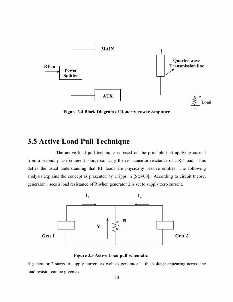
Figure 3.4 Block diagram of Doherty power amplifier……………………………. 20
Figure 3.5 Active load-pull schematic……………………………………………... 20
Figure 3.6 Two way Doherty Schematic…………………………………………... 22
Figure 3.7 Doherty Amplifier Circuit……………………………………………… 25
Figure 3.8 Block Diagram DPA…………………………………………………… 27
Figure 3.9 Current and voltage characteristics of DPA……………………………. 28
Figure 3.10 Stage I – Operation of Doherty power Amplifier……………………………. 29
Figure 3.11 Stage II– Operation of Doherty power Amplifier…………………………… 30
Figure 3.12 Stage III– Operation of Doherty power Amplifier………………………….. 30
Figure 3.13 Ideal Efficiency plot of Doherty power amplifier…………………….. 32
Figure 4.1 Architecture of the Doherty amplifier………………………………….. 35
Figure 4.2 Current and voltage characteristics of DPA……………………………
Figure 4.3 Input and output matching of Main and Auxiliary amplifier…………………
36
37
viii
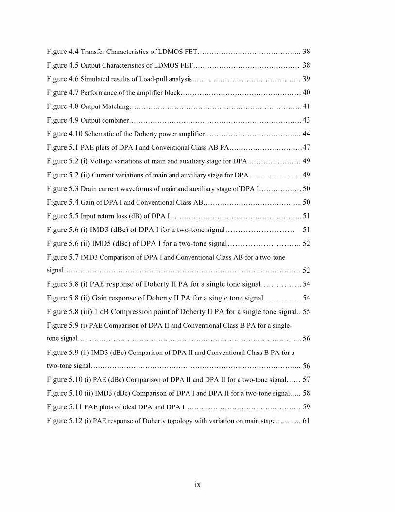
Figure 4.4 Transfer Characteristics of LDMOS FET…………………………………….. 38
Figure 4.5 Output Characteristics of LDMOS FET……………………………………… 38
Figure 4.6 Simulated results of Load-pull analysis………………………………………. 39
Figure 4.7 Performance of the amplifier block…………………………………………… 40
Figure 4.8 Output Matching………………………………………………………………. 41
Figure 4.9 Output combiner………………………………………………………………. 43
Figure 4.10 Schematic of the Doherty power amplifier………………………………….. 44
Figure 5.1 PAE plots of DPA I and Conventional Class AB PA…………………………. 47
Figure 5.2 (i) Voltage variations of main and auxiliary stage for DPA …………………. 49
Figure 5.2 (ii) Current variations of main and auxiliary stage for DPA ………………… 49
Figure 5.3 Drain current waveforms of main and auxiliary stage of DPA I……………… 50
Figure 5.4 Gain of DPA I and Conventional Class AB…………………………………... 50
Figure 5.5 Input return loss (dB) of DPA I……………………………………………….. 51
Figure 5.6 (i) IMD3 (dBc) of DPA I for a two-tone signal……………………… 51
Figure 5.6 (ii) IMD5 (dBc) of DPA I for a two-tone signal……………………….. 52
Figure 5.7 IMD3 Comparison of DPA I and Conventional Class AB for a two-tone
signal……………………………………………………………………………………….
52
Figure 5.8 (i) PAE response of Doherty II PA for a single tone signal……………. 54
Figure 5.8 (ii) Gain response of Doherty II PA for a single tone signal…………… 54
Figure 5.8 (iii) 1 dB Compression point of Doherty II PA for a single tone signal.. 55
Figure 5.9 (i) PAE Comparison of DPA II and Conventional Class B PA for a single-
tone signal…………………………………………………………………………………..
56
Figure 5.9 (ii) IMD3 (dBc) Comparison of DPA II and Conventional Class B PA for a
two-tone signal……………………………………………………………………………..
56
Figure 5.10 (i) PAE (dBc) Comparison of DPA II and DPA II for a two-tone signal…… 57
Figure 5.10 (ii) IMD3 (dBc) Comparison of DPA I and DPA II for a two-tone signal….. 58
Figure 5.11 PAE plots of ideal DPA and DPA I…………………………………………. 59
Figure 5.12 (i) PAE response of Doherty topology with variation on main stage……….. 61
ix

Figure 5.12 (iii) Gain response of Doherty topology with variation of main stage bias….
63
Figure 5.13 (i) PAE response of DPA for a single-tone signal…………………………..
64
Figure 5.13 (ii) Gain response of DPA for a single-tone signal………………………….
65
Figure 5.13 (iii) PAE response of Doherty topology with variation on main stage bias…
66
Figure 5.13 (iv) IMD3 response of DPA for two-tone signal………………………
66
x

List of Tables Table 4.1 Gate bias Voltages corresponding to different classes of Operation…………... 41 Table 5.1 Doherty amplifier I Bias points………………………………………………… 47 Table 5.2 RF Performances of DPA I with variation in input power…………………….. 48 Table 5.3 RF responses of DPA I and Class AB power amplifier………………… 53 Table 5.4 Doherty amplifier II Bias points………………………………………………. 53 Table 5.5 Output impedance of the main & auxiliary stages with variation in i/p power... 60 Table 5.6 Biasing Voltage range corresponding to each class of operation………………. 61
xi
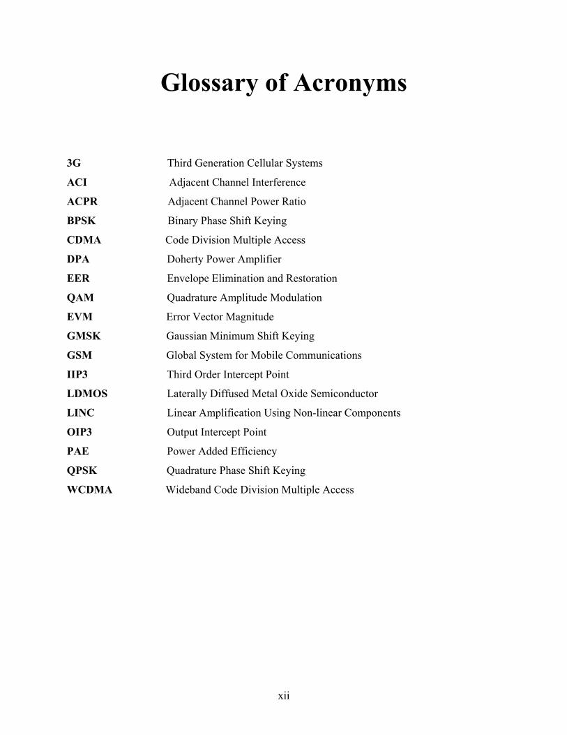
Glossary of Acronyms
3G Third Generation Cellular Systems
ACI Adjacent Channel Interference
ACPR Adjacent Channel Power Ratio
BPSK Binary Phase Shift Keying
CDMA Code Division Multiple Access
DPA Doherty Power Amplifier
EER Envelope Elimination and Restoration
QAM Quadrature Amplitude Modulation
EVM Error Vector Magnitude
GMSK Gaussian Minimum Shift Keying
GSM Global System for Mobile Communications
IIP3 Third Order Intercept Point
LDMOS Laterally Diffused Metal Oxide Semiconductor
LINC Linear Amplification Using Non-linear Components
OIP3 Output Intercept Point
PAE Power Added Efficiency
QPSK Quadrature Phase Shift Keying
WCDMA Wideband Code Division Multiple Access
xii
1
Chapter 1
Introduction
1.1 Background High efficiency and good linearity are among the very important characteristics of a
base station power amplifier used in majority of the modern applications such as IS-95, CDMA-
2000 and WCDMA. Both the characteristics have always been conflicting requirements
demanding innovative power amplifier design techniques. Maintaining the high efficiency
attained, over a wide range of the power amplifier operation is an added requirement in these
applications making power amplifier design a challenging task.
Spectrum is expensive, and newer technologies demand transmission of maximum
amount of data using the minimum amount of spectrum. This requires sophisticated modulation
techniques, leading to wide, dynamic signals that require linear amplification. Although linear
amplification is achievable, it always comes at the expense of efficiency.
2
The modern wireless communication standards employ non-constant envelope
modulation techniques such as quadrature phase shift keying (QPSK) for attaining high data
rates and spectral efficiency. The RF power amplifiers implemented in such systems are ‘backed
off’ from its saturation into their linear operating region in order to obtain a satisfactory linearity
over the transmitter’s dynamic range. This drastically reduces the efficiency of the power
amplifier decreasing the battery life of the handset. At present, a more routine approach to this
issue is to design a high efficiency amplifier with a non-linear mode combined with a more
complex linearity improvement technique.
1.2 Research Goals In this research project, the different possible implementations of high efficiency power
amplifiers using the Doherty topology are investigated without compromising on the stringent
linearity requirement of the 3G WCDMA standards. The main goals of the research are listed
here:
• Detailed analysis of the possible implementation techniques of modern Doherty
amplifiers using solid state devices in comparison to the conventional design built using
vaccum tubes
• A detailed methodology for the design of a two stage Doherty power amplifier using
Motorola HV4_FET transistors
• Design and simulation of two different realizations of the Doherty power amplifier for
WCDMA band with a center frequency of 2.14 GHz and bandwidth of 5 MHz using
Motorola LDMOS transistors developed with HV4 process technology.
• Analysis of the effect of biasing of the main and auxiliary stages of the Doherty power
amplifier on efficiency and linearity
• Literature review of implementation of techniques like derivative superposition on
Doherty power amplifier for enhancement of linearity
3
1.3 Report Organization This report has two major goals: first, to provide the reader with an introduction on the
principle of a two stage Doherty power amplifier; and second, to discuss its performance in
comparison with a classical power amplifier design. The format of this report will therefore
follow the goals.
Chapter 2 discusses the common topologies used in Power Amplifier design, as well as
briefly explains some common design parameters involved in the design of a power amplifier.
Chapter 2 also mentions some of the important properties of an LDMOS transistor.
Chapter 3 contains the principle of Doherty technique with brief review on the history
of Doherty power amplifiers built using vaccum tubes. A discussion on the working of an ideal
Doherty power amplifier has also been provided.
Chapter 4 explains in detail the design and implementation of a two stage Doherty
amplifier using LDMOS FETs.
Chapter 5 will discuss the simulation results that were obtained from two different
realizations of the Doherty design. A comparative analysis on the performance of the proposed
designs with the corresponding classical power amplifier design has also been provided. Finally,
conclusions from this work will be presented in Chapter 6.
4
Chapter 2
RF Power Amplifiers 2.1 Classes of PA Operation LDMOS power amplifiers used in transceiver circuits exhibits varying degrees of
nonlinearity, depending on its class of operation. The output current’s harmonic content varies
with the DC bias at the gate of the LDMOS device, while maintaining a constant RF input signal.
In certain applications, it may be desirable to have the transistor conducting for only a certain
portion of the input signal. The portion of the input RF signal for which there is an output current
determines the class of operation of a power amplifier. This chapter discusses four classes of
power amplifier operation, which are predominantly used in Doherty power amplifiers. Figure
2.1 shows the typical classes based on the transistor transfer characteristics.
C AB
B
A
Figure 2.1 Classes of operation of Power amplifier based on transfer characteristics
2.1.1 Class A Class A amplifiers are biased such that the variations in input signal occur within
the limits of cutoff and saturation [a]. The collector current flows during the complete cycle (360
degrees) of the input signal.
.
Figure 2.2 Class A Transfer characteristics [Grig00]
5
As shown in Figure 2.1, the bias point is set closer to the center of the transistor’s range of
operation also called as the active region. Class A operation provides the maximum linearity in
comparison to any other class of operation
2.1.2 Class B The collector (drain) current flowing during one-half of the RF input signal
signifies the class B operation. The dc operating point is set so that the base (gate) current is zero
with no RF input signal. This is achieved by biasing the transistor at its cut-off voltage and any
current through the device goes directly to the load. Precisely, the conduction angle of the class
B amplifier operation remains 180 degrees, or one half the input cycle. Class B power amplifiers
are often implemented using push-pull configuration, which uses two transistors in parallel; each
amplifying one half of the RF input signal.
Figure 2.3 Class B Transfer characteristics [Grig00]
6
As a result, the efficiency of the class B amplifier is almost double than its
equivalent class A amplifier. Although this architecture greatly improves the efficiency, it is
normally used in applications with less stringent linearity requirements. Usually, the current
waveforms are heavily distorted and a large Q tank circuit is required to recover the sinusoid.
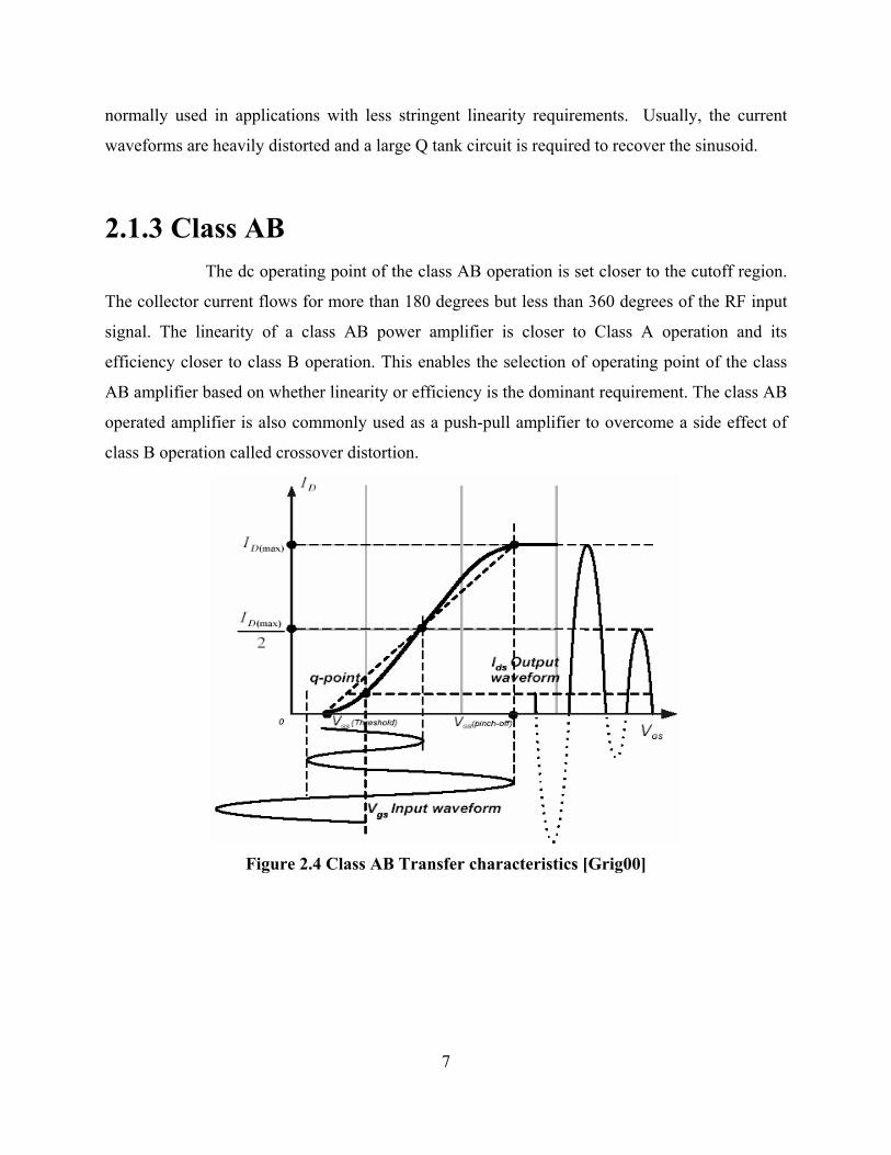
2.1.3 Class AB The dc operating point of the class AB operation is set closer to the cutoff region.
The collector current flows for more than 180 degrees but less than 360 degrees of the RF input
signal. The linearity of a class AB power amplifier is closer to Class A operation and its
efficiency closer to class B operation. This enables the selection of operating point of the class
AB amplifier based on whether linearity or efficiency is the dominant requirement. The class AB
operated amplifier is also commonly used as a push-pull amplifier to overcome a side effect of
class B operation called crossover distortion.
Figure 2.4 Class AB Transfer characteristics [Grig00]
7

8
2.1.4 Class C In class C operation, drain current flows for less than one half cycle of the input
signal. The Class C operation is achieved by setting the dc operating point below cutoff and
thereby, allowing conduction on only the portion of the input signal that overcomes the reverse
bias of the source gate junction. Although linearity is the worst, the efficiency of class C is the
highest of the four classes of amplifier operations discussed.
2.1.5 Other High Efficiency classes There are other high efficiency classes of operation such as Class D, E and F. These
classes of operation are more suited for applications using constant envelope modulation
techniques with linearity being a less stringent requirement. Doherty technique involves the
implementation of an efficiency enhancement on a linear power amplifier circuit such as Class A
or AB.
2.2 Characteristics of Power Amplifiers 2.2.1 Linearity The RF power amplifiers are inherently non-linear and are the main contributors for
distortion products in a transceiver chain. Power amplifiers effect the utilization of the spectrum
through nonlinear performance. Non-linearity is typically caused due to the compression
behavior of the power amplifier, which occurs when the RF transistor operates in its saturation
region due to a certain high input level.
2.2.2 Measurement of Linearity The non-linearity of a power amplifier can be attributed mainly to gain compression
and harmonic distortions resulting in imperfect reproduction of the amplified signal. It is
characterized by various techniques depending upon specific modulation and application. Some
of the widely used figures for quantifying linearity are the
• 1 dB compression point
• Third order intermodulation distortion
• Third order intercept point (IIP3)
• Adjacent channel power ratio (ACPR)
• Error vector Magnitude (EVM)
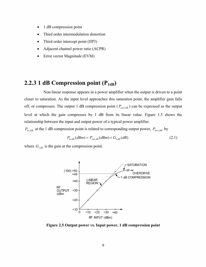
2.2.3 1 dB Compression point (P1dB) Non-linear response appears in a power amplifier when the output is driven to a point
closer to saturation. As the input level approaches this saturation point, the amplifier gain falls
off, or compresses. The output 1 dB compression point ( ) can be expressed as the output
level at which the gain compresses by 1 dB from its linear value. Figure 1.5 shows the
relationship between the input and output power of a typical power amplifier.
dBoutP 1,
dBinP 1, at the 1 dB compression point is related to corresponding output power, by dBoutP 1,
)()()( ,1,, dBGdBmPdBmP dBdBoutdBin += (2.1)
where is the gain at the compression point. dBG ,1
Figure 2.5 Output power vs. Input power, 1 dB compression point
9
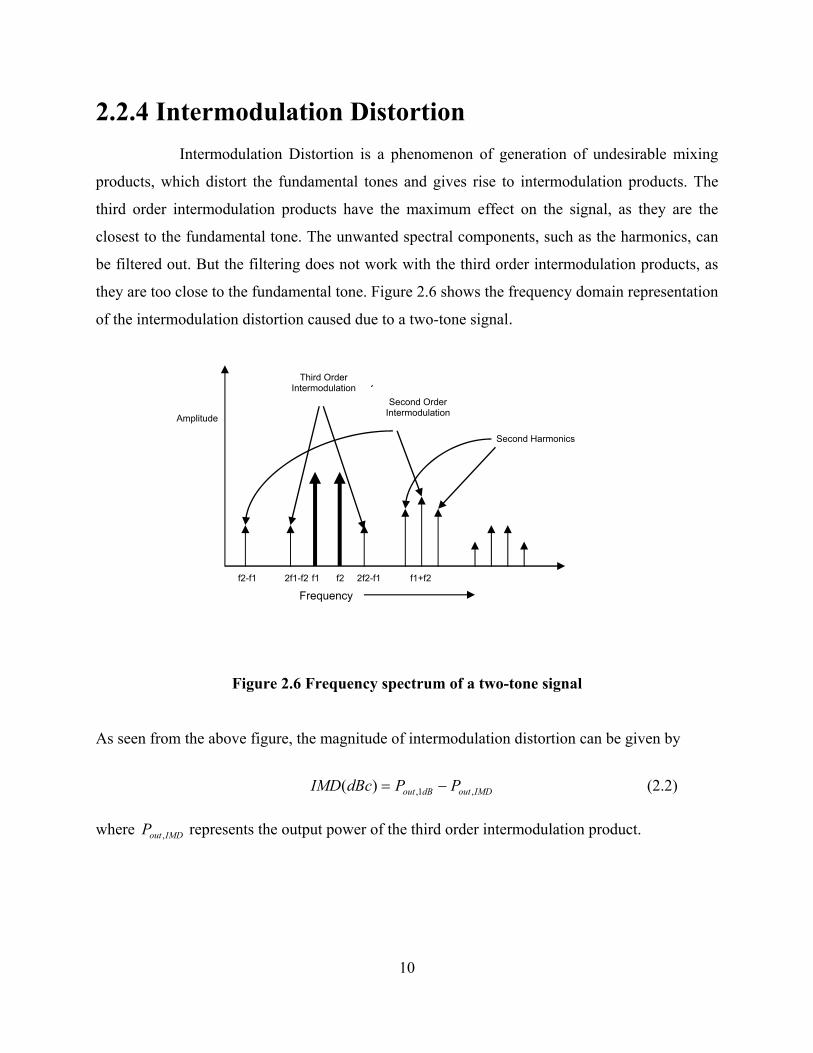
2.2.4 Intermodulation Distortion Intermodulation Distortion is a phenomenon of generation of undesirable mixing
products, which distort the fundamental tones and gives rise to intermodulation products. The
third order intermodulation products have the maximum effect on the signal, as they are the
closest to the fundamental tone. The unwanted spectral components, such as the harmonics, can
be filtered out. But the filtering does not work with the third order intermodulation products, as
they are too close to the fundamental tone. Figure 2.6 shows the frequency domain representation
of the intermodulation distortion caused due to a two-tone signal.
Third Order Intermodulation
`
Second Order IntermodulationAmplitude
Second Harmonics
10
Figure 2.6 Frequency spectrum of a two-tone signal
As seen from the above figure, the magnitude of intermodulation distortion can be given by
IMDoutdBout PPdBcIMD ,1,)( −= (2.2)
where represents the output power of the third order intermodulation product. IMDoutP ,
Frequency f1 f22f1-f2 2f2-f1f2-f1 f1+f2
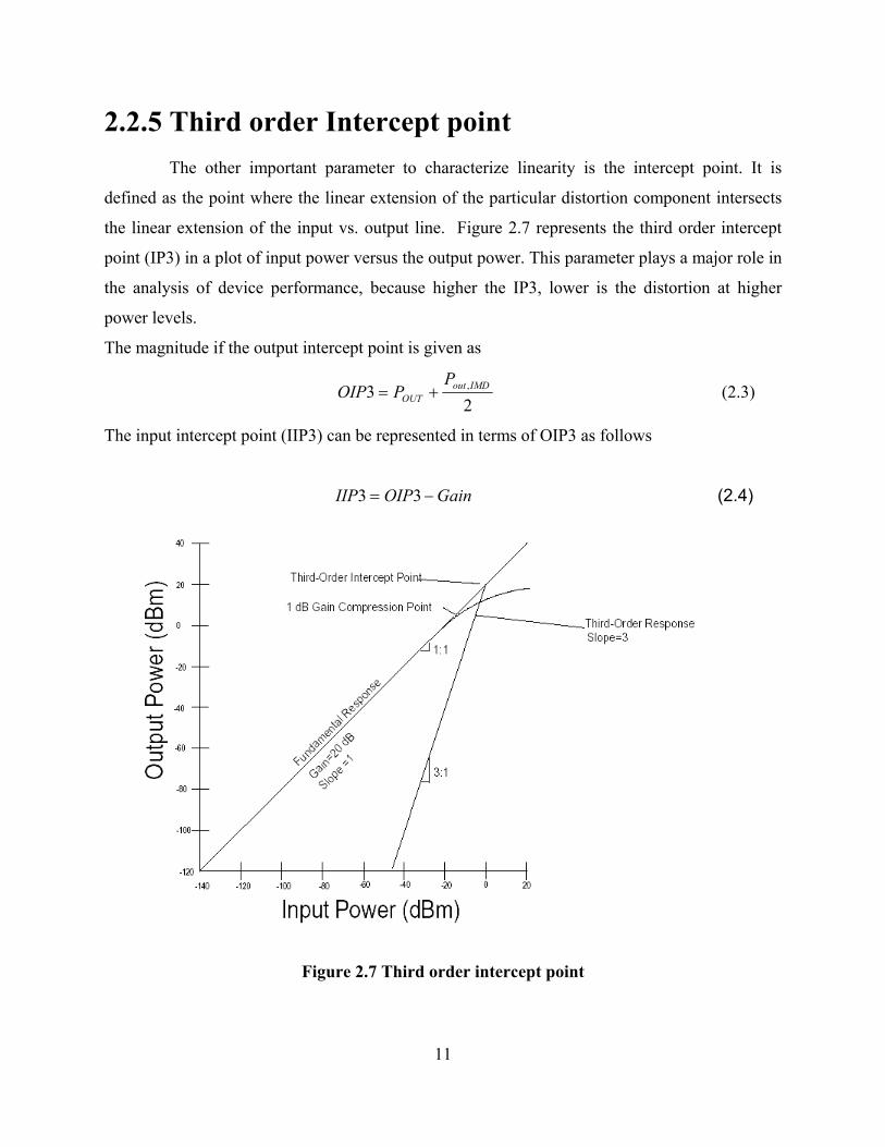
2.2.5 Third order Intercept point The other important parameter to characterize linearity is the intercept point. It is
defined as the point where the linear extension of the particular distortion component intersects
the linear extension of the input vs. output line. Figure 2.7 represents the third order intercept
point (IP3) in a plot of input power versus the output power. This parameter plays a major role in
the analysis of device performance, because higher the IP3, lower is the distortion at higher
power levels.
The magnitude if the output intercept point is given as
2
3 ,IMDoutOUT
PPOIP += (2.3)
The input intercept point (IIP3) can be represented in terms of OIP3 as follows
GainOIPIIP −= 33 (2.4)
Figure 2.7 Third order intercept point 11
2.2.6 Efficiency Efficiency in power amplifiers is expressed as the part of the dc power that is
converted to RF power, and there are three definitions of efficiency that are commonly used.
Drain efficiency is the ratio of the RF-output power to the dc input power.
dc
OUT
PP
=η (2.5)
Power-added efficiency (PAE), however, takes the power of the input signal into account and
can be expressed by
dc
INOUT
PPPPAE −
=
PAE is generally used for analyzing PA performance when the gain is high. Finally, the overall
efficiency is represented as
INdc
OUToverall PP
PP
+= (2.7)
and this form of efficiency is usable for all kinds of performance evaluations.
2.2.7 Noise Noise is of very little importance in design of power amplifiers. The formula for
the noise factor of a cascaded system is given by
IN
Ntot GGG
FGG
FG
FFF
−
−++
−+
−+=
...1
...11
2121
3
1
21 (2.8)
As can be seen from the above formula, the noise factor basically depends on the first few stages.
The power amplifier usually being the last component of the transmitter chain has very little
impact on the overall noise figure.
12
2.3 LDMOS Power Transistors Laterally Diffused Metal-Oxide-Semiconductor (LDMOS) devices are
enhancement mode Nchannel MOSFETs. The device cross section is designed for high voltage
operation with low parasitic capacitance to enable high frequency operation. The length of the
channel usually determines the high frequency properties of the LDMOS transistors. The shorter
channel length improves the linearity. LDMOS technology is intended to replace bipolar
transistors in many high-power telecommunication applications. It had been engineered to
achieve better gain, lower third order intermodulation distortion and higher operating efficiencies
over a large dynamic range. These features of the LDMOS device enable fewer gain stages in RF
power amplifiers and better efficiency. Figure 2.8 provides a performance comparison between
the LDMOS and Bipolar transistors [Phil00].
Figure 2.8 Performance comparisons of LDMOS (Solid line) and BJT (dotted line)
(Gain and linearity plots of a class AB PA) [Phil00]
13
14
The exceptional linearity of the LDMOS transistors makes them the best fit to
meet the stringent linearity requirements of the 3G standards. LDMOS devices significantly
reduce power consumption and thermal issues in state-of-the-art 3G base stations achieving a
50% higher power density, a 6-8% higher WCDMA efficiency and a 2dB higher power gain than
previous 0.8um technologies [Phil00].
2.4 Conclusion The performance of a transceiver in mobile communications depends primarily
on the performance of the power amplifier. High gain, high linearity, stability and high
efficiency are the characteristics of a well-designed power amplifier. The objective of this
research, as stated earlier, is to design a highly efficient power amplifier for the WCDMA (2.11
– 2.17 GHz) band using the Doherty topology without compromising on the linearity
requirements. The following chapters will provide a detailed analysis of the Doherty technique,
with the simulated designs and results.
15
Chapter 3
Doherty Power Amplifiers
3.1 Introduction The most efficient operation of a power amplifier is near compression. This is
one of the well-known advantages of standards like GSM, which employs constant envelope
modulation technique like GMSK. Such modulation techniques ensure that the envelope of the
transmitted signal is constant. This enables the power amplifier of the mobile system to operate
near saturation without distortion. On the other hand, modern standards like EDGE with more
efficient data rates use modulation techniques like BPSK, QPSK, and QAM. These techniques
produce non-constant envelope signals, which require the power amplifier to operate in the linear
region, 3 to 6 dB backed off from compression. This prevents spectrum splatter of sideband
components that might cause Adjacent Channel Interference (ACI), thereby making high
efficiency hard to achieve.
Power amplification of amplitude-modulated signals has two main drawbacks.
Firstly, the modulating signal gets distorted when the power amplifier is used at its full rated RF
power level. Secondly, maximum efficiency is attained only at one single power level, usually
closer to the maximum rated power of the device. An implementation of efficiency enhancement
16
technique that results in a very high efficiency in the linear region of operation of the power
amplifier is the solution for the both the above issues.
Several efficiency enhancement techniques have been suggested to date. The
Doherty power amplifier is considered the best choice because other efficiency enhancing
techniques like Kahn (Envelope Elimination and Restoration), dynamic envelope tracking, or the
Linear amplification using Non linear components (LINC) Technique degrade linearity, raise
cost and provide narrow bandwidth.
Envelope elimination and restoration (EER) techniques use a combination of
highly efficient envelope amplifier and a non-linear amplifier to provide a highly efficient and
linear power amplifier. Such an amplifier typically consists of a limiter that eliminates the
envelope and a highly efficient non-linear PA like Class C or Class D for the amplification of the
resulting constant amplitude phase modulated carrier. A constant envelope enables the non-linear
amplifier to operate near compression without any distortion, enhancing its efficiency. Finally,
amplitude modulation of a highly linear PA restores the envelope of the phase-modulated signal.
Envelope tracking is a method similar to the EER technique. It uses a dynamically varying
supply voltage that conserves power while allowing the PA to operate in linear mode. The RF
drive power contains both amplitude and phase information, and the burden of linearity lies
entirely on the final power amplifier. Though the performance of envelope tracking is better than
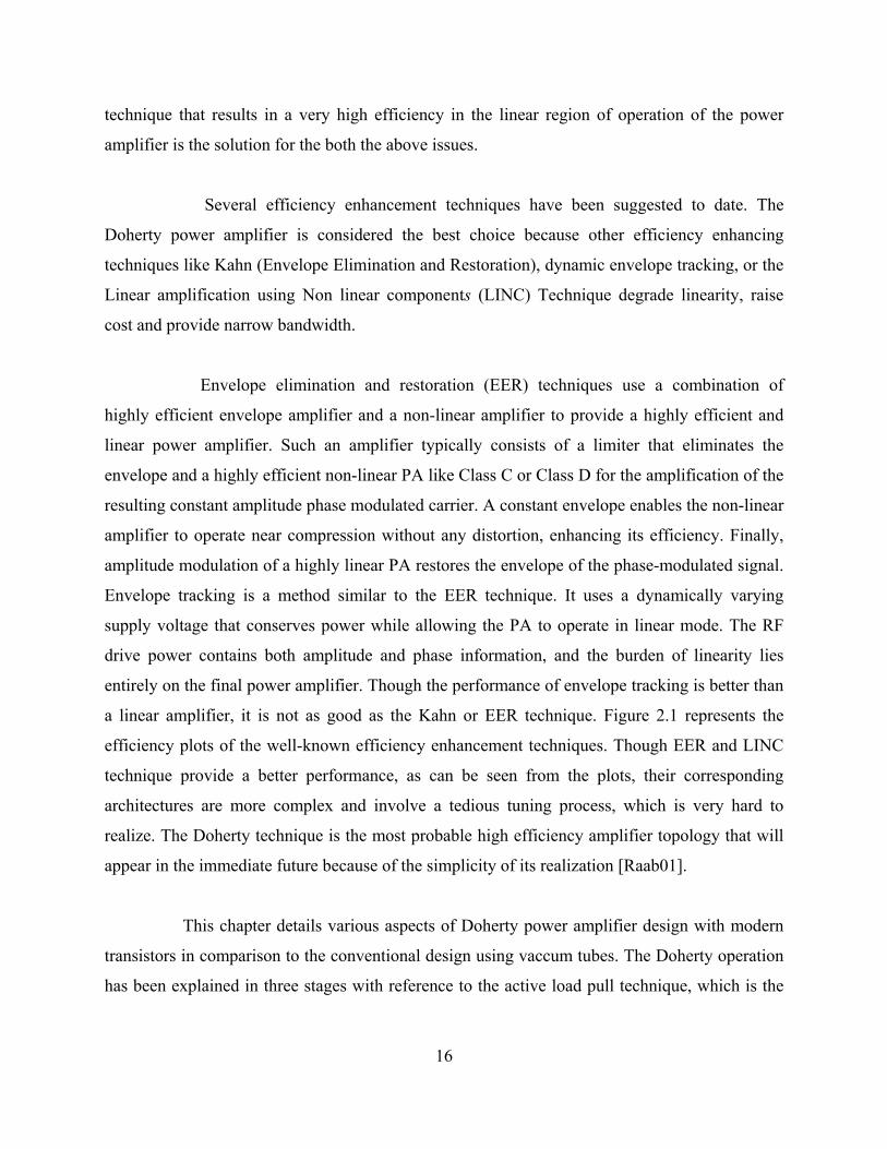
a linear amplifier, it is not as good as the Kahn or EER technique. Figure 2.1 represents the
efficiency plots of the well-known efficiency enhancement techniques. Though EER and LINC
technique provide a better performance, as can be seen from the plots, their corresponding
architectures are more complex and involve a tedious tuning process, which is very hard to
realize. The Doherty technique is the most probable high efficiency amplifier topology that will
appear in the immediate future because of the simplicity of its realization [Raab01].
This chapter details various aspects of Doherty power amplifier design with modern
transistors in comparison to the conventional design using vaccum tubes. The Doherty operation
has been explained in three stages with reference to the active load pull technique, which is the
underlying principle of Doherty power amplifiers. For better understanding, all the derivations in
this chapter correspond to ideal behavior of Doherty technique.
17
Figure 3.1 Performance analyses of efficiency enhancement techniques
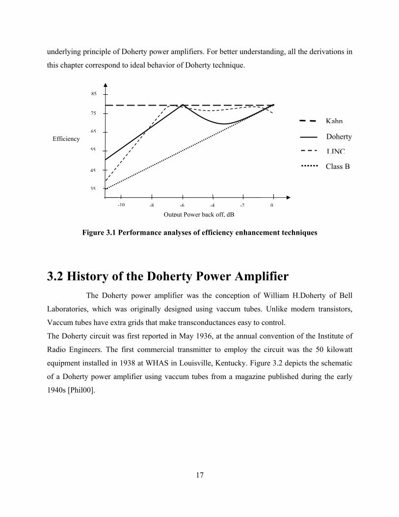
3.2 History of the Doherty Power Amplifier The Doherty power amplifier was the conception of William H.Doherty of Bell
Laboratories, which was originally designed using vaccum tubes. Unlike modern transistors,
Vaccum tubes have extra grids that make transconductances easy to control.
The Doherty circuit was first reported in May 1936, at the annual convention of the Institute of
Radio Engineers. The first commercial transmitter to employ the circuit was the 50 kilowatt
equipment installed in 1938 at WHAS in Louisville, Kentucky. Figure 3.2 depicts the schematic
of a Doherty power amplifier using vaccum tubes from a magazine published during the early
1940s [Phil00].
85
75
65
55
45
35
0-2-4-6-8-10
Kahn
Doherty Efficiency
LINC
Class B
Output Power back off, dB
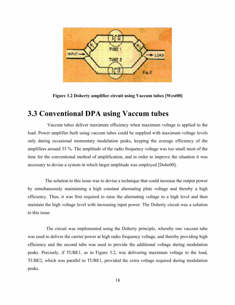
Figure 3.2 Doherty amplifier circuit using Vaccum tubes [West00]
3.3 Conventional DPA using Vaccum tubes Vaccum tubes deliver maximum efficiency when maximum voltage is applied to the
load. Power amplifier built using vaccum tubes could be supplied with maximum voltage levels
only during occasional momentary modulation peaks, keeping the average efficiency of the
amplifiers around 33 %. The amplitude of the radio frequency voltage was too small most of the
time for the conventional method of amplification, and in order to improve the situation it was
necessary to devise a system in which larger amplitude was employed [Dohe00].
The solution to this issue was to devise a technique that could increase the output power
by simultaneously maintaining a high constant alternating plate voltage and thereby a high
efficiency. Thus, it was first required to raise the alternating voltage to a high level and then
maintain the high voltage level with increasing input power. The Doherty circuit was a solution
to this issue.
The circuit was implemented using the Doherty principle, whereby one vaccum tube
was used to deliver the carrier power at high radio frequency voltage, and thereby providing high
efficiency and the second tube was used to provide the additional voltage during modulation
peaks. Precisely, if TUBE1, as in Figure 3.2, was delivering maximum voltage to the load,
TUBE2, which was parallel to TUBE1, provided the extra voltage required during modulation
peaks.
18
19
TUBE 1 TUBE 2
Impedance Inverting Network 2R
Figure 3.3 High efficiency configuration using Vaccum tubes [Dohe00]
Figure 3.3 represents the Doherty circuit with an impedance-inverting network, the role of which
will be explained in detail in the following section.
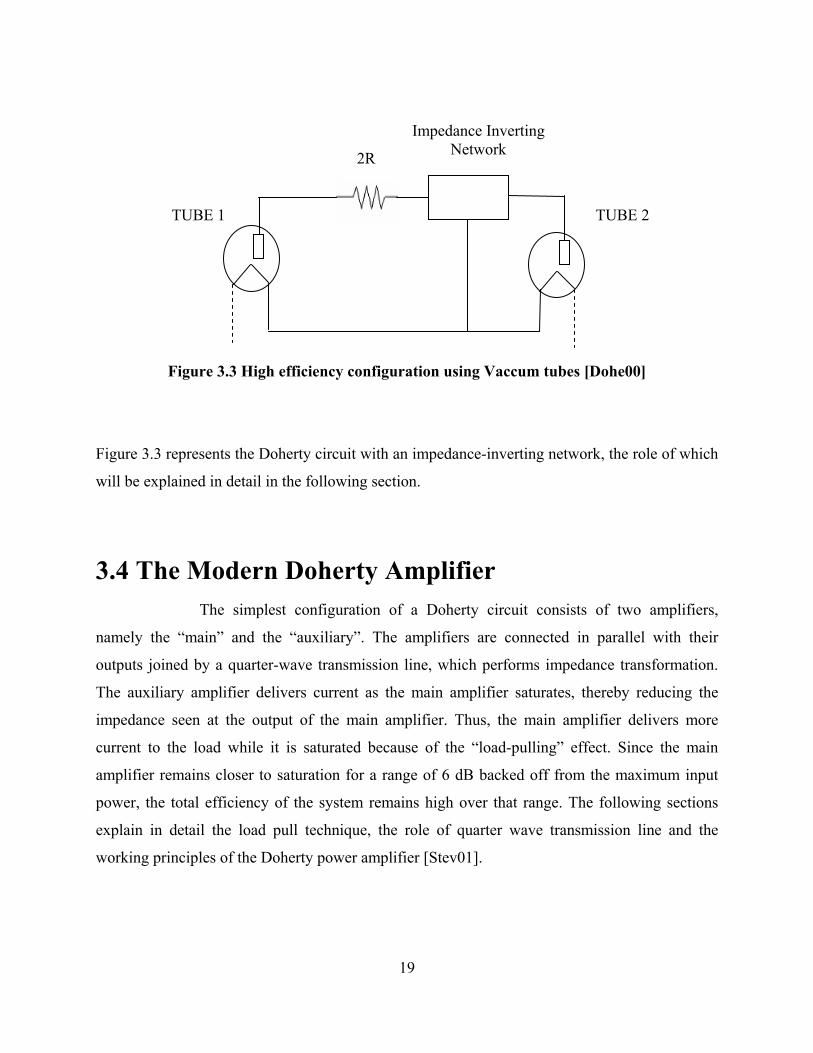
3.4 The Modern Doherty Amplifier The simplest configuration of a Doherty circuit consists of two amplifiers,
namely the “main” and the “auxiliary”. The amplifiers are connected in parallel with their
outputs joined by a quarter-wave transmission line, which performs impedance transformation.
The auxiliary amplifier delivers current as the main amplifier saturates, thereby reducing the
impedance seen at the output of the main amplifier. Thus, the main amplifier delivers more
current to the load while it is saturated because of the “load-pulling” effect. Since the main
amplifier remains closer to saturation for a range of 6 dB backed off from the maximum input
power, the total efficiency of the system remains high over that range. The following sections
explain in detail the load pull technique, the role of quarter wave transmission line and the
working principles of the Doherty power amplifier [Stev01].
20
Figure 3.4 Block Diagram of Doherty Power Amplifier
N
Load AUX
Quarter wave Transmission line
Power Splitter
RF in
3.5 Active Load Pull Technique The active load pull technique is based on the principle that applying current
from a second, phase coherent source can vary the resistance or reactance of a RF load. This
defies the usual understanding that RF loads are physically passive entities. The following
analysis explains the concept as presented by Cripps in [Stev00]. According to circuit theory,
generator 1 sees a load resistance of R when generator 2 is set to supply zero current.
I2I1
V
Gen 1
If generator 2 starts to supply current as well as generator 1, the voltage
load resistor can be given as
Figure 3.5 Active Load pull schematic
MAI
Gen 2
appearing across the
(3.1) [ ]21L RV II +=
With the addition of supply current to the load resistance from second generator, the resistance
seen by generator 1 now becomes
(3.2) ⎥⎦
⎤⎢⎣
⎡ +=
1
211 I
IIRR
Likewise, the resistance seen by generator 2 can be represented as
⎥⎦
⎤⎢⎣
⎡ +=
2
212 I
IIRR (3.3)
The above concept can be extended to ac circuits by using complex notation for representing the
magnitude and the phase of the currents and voltages and the resistive and reactive components.
Thus, equation 3.3 can be represented as
(3.4)
⎟⎟⎠
⎞⎜⎜⎝
⎛+=
2
11 1
II
RZ
Z1 can be transformed to higher value if I2 is made in phase with I1 and to a smaller value if I2 is
made antiphase with I1.
The concept of load pull technique can be implemented with transistors if the
generators are replaced by the output transconductances of the RF transistors. Thus, when two
transistors are connected in parallel, one can modify the impedance seen by the other through
proper biasing. This concept extended to the combination of two unlike devices with different
periphery and biasing results in the Doherty configuration.
21
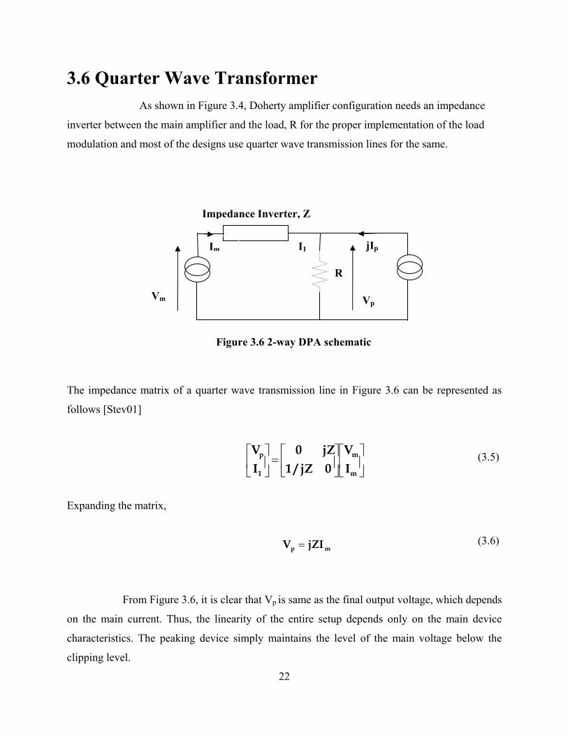
3.6 Quarter Wave Transformer As shown in Figure 3.4, Doherty amplifier configuration needs an impedance
inverter between the main amplifier and the load, R for the proper implementation of the load
modulation and most of the designs use quarter wave transmission lines for the same.
22
The impedance matrix of a quarter wave transmission line in Figure 3.6 can be represented as
follows [Stev01]
Expanding the matrix,
From Figure 3.6, it is clear that Vp is same as the final output voltage, which depends
on the main current. Thus, the linearity of the entire setup depends only on the main device
characteristics. The peaking device simply maintains the level of the main voltage below the
clipping level.
RR 1
Im
Impedance Inverter, Z
jIp I1
R
Vm Vp
Figure 3.6 2-way DPA schematic
⎥⎦
⎤⎢⎣
⎡⎥⎦
⎤⎢⎣
⎡=⎥
⎦
⎤⎢⎣
⎡
m
m
1
p
IV
0jZ/1jZ0
IV
mp jZIV = (3.6)
(3.5)
This can be represented using the equations as follows.
(3.7) m
01 V
JZ1I =
Where I1 is related to Ip by
(3.8) 1
pp I
RV
jI +=
Thus, the action of the peaking amplifier on the main amplifier can be consolidated
using the equation
(3.9) ⎥⎦
⎤⎢⎣
⎡ −⎟⎠⎞
⎜⎝⎛= pmm IIRZZV
The role of the quarter wave transmission line can be appreciated more once the
working principle of DPA is explained. It enables the decrease of the impedance seen by the
main amplifier once the main voltage reaches saturation, thereby increasing the flow of the
current and thus maintaining the efficiency.
3.7 Characteristic impedance calculation As discussed earlier, the main concept behind the Doherty technique is to enhance
the efficiency of a power amplifier for a wider range of input signals as compared to the standard
case where maximum efficiency is attained only at peak power. This is achieved by the
premature saturation of the main amplifier, which in turn is achieved by making it see very high
23
impedance by the action of the quarter wave transformer and using the peaking amplifier to
reduce the high impedance seen by the main amplifier, thereby maintaining the maximum
voltage of the main amplifier. This concept will be explained in detail in the next section.
Before proceeding to the working principle of Doherty power amplifier, it is
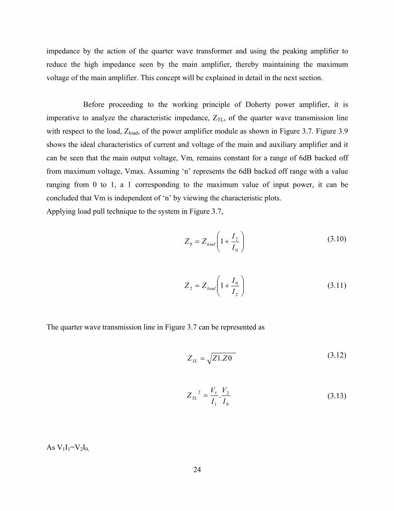
imperative to analyze the characteristic impedance, ZTL, of the quarter wave transmission line
with respect to the load, Zload, of the power amplifier module as shown in Figure 3.7. Figure 3.9
shows the ideal characteristics of current and voltage of the main and auxiliary amplifier and it
can be seen that the main output voltage, Vm, remains constant for a range of 6dB backed off
from maximum voltage, Vmax. Assuming ‘n’ represents the 6dB backed off range with a value
ranging from 0 to 1, a 1 corresponding to the maximum value of input power, it can be
concluded that Vm is independent of ‘n’ by viewing the characteristic plots.
Applying load pull technique to the system in Figure 3.7,
⎟⎟⎞
⎜⎛
= 2IZZ
⎠⎜⎝+
00 1
Iload
24
⎟⎟⎠
⎞⎜⎜⎝
⎛+=
2
02 1
II
ZZ load
The quarter wave transmission line in Figure 3.7 can be represented as
0.1 ZZZ =TL (3.12)
(3.11)
(3.10)
(3.13) 0
2
1
12 .IV
IVZTL =
As V1I1=V2I0,
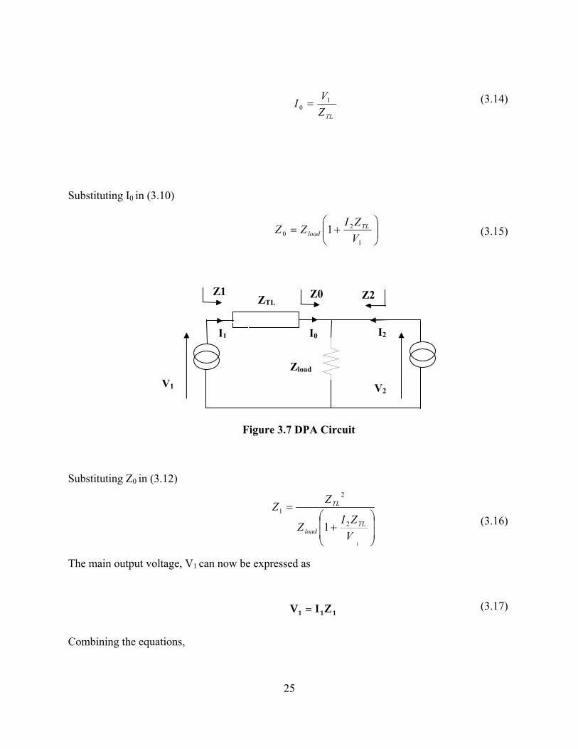
(3.14) TLZ
VI 1
0 =
Substituting I0 in (3.10)
⎟⎟⎠
⎞⎜⎜⎝
⎛+=
1
20 1
VZI
ZZ TLload (3.15)
25
Substituting Z0 in (3.12)
The main output voltage, V1 can now be expressed as
Combining the equations,
Figure 3.7 DPA Circuit
RR 1
I1 I2
ZTL
I0
Z1 Z0 Z2
Zload
V1 V2
⎟⎟
⎠
⎞
⎜⎜
⎝
⎛+
=
1
2
2
1
1VZI
Z
ZZ
TLload
TL
(3.16)
(3.17) 111 ZIV =
26
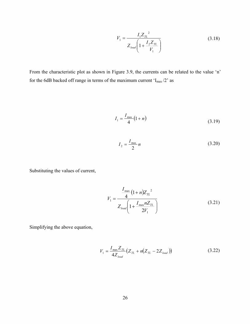
From the characteristic plot as shown in Figure 3.9, the currents can be related to the value ‘n’
for the 6dB backed off range in terms of the maximum current ‘Imax /2’ as
⎟⎟⎠
⎞⎜⎜⎝
⎛+
=
1
2
21
1
1VZIZ
ZIVTL
load
TL
( )nI
I += 14max
1
nI
I2max
2 =
( )
⎟⎟⎠
⎞⎜⎜⎝
⎛+
+=
1
max
2max
1
21
14
VnZI
Z
ZnI
VTL
load
TL
(( loadTLTLload
TL ZZnZZ
ZIV 2
4max
1 −+= )) (3.22)
(3.21)
(3.20)
(3.19)
(3.18)
Substituting the values of current,
Simplifying the above equation,
As stated earlier, efficiency enhancement is attained in the 6dB backed off range if
V1 remains constant, and thus needs to be independent of the factor ‘n’. Thus from the above
equation, it can be inferred that
27
loadTL ZZ 2
= (3.23)
Thus for the optimum operation of the Doherty configuration, the characteristic
impedance of the quarter wave transmission line needs to be twice the resistive load. This
enables the main amplifier to view twice the output impedance enabling it to reach the maximum
voltage when the current is only half the maximum value.
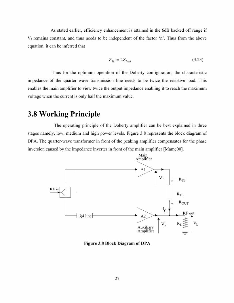
3.8 Working Principle The operating principle of the Doherty amplifier can be best explained in three
stages namely, low, medium and high power levels. Figure 3.8 represents the block diagram of
DPA. The quarter-wave transformer in front of the peaking amplifier compensates for the phase
inversion caused by the impedance inverter in front of the main amplifier [Mamc00]. Main Amplifier
Vp VLR L
utRF o
RF in
λ /4 line A2
R TL
A1
R IN Vm
R OUT
0 I
Auxiliary Amplifier
Figure 3.8 Block Diagram of DPA
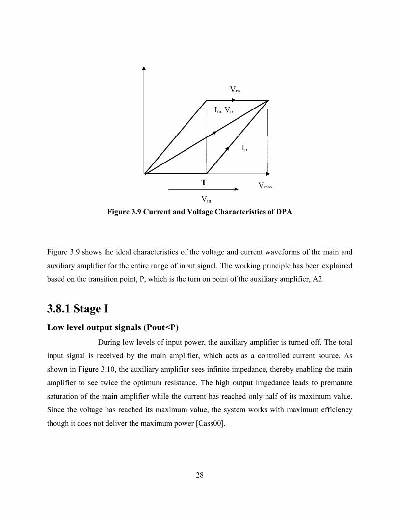
Figure 3.9 Current and Voltage Characteristics of DPA
T
Im, Vp
Vm
Vin
Vmax
Ip
Figure 3.9 shows the ideal characteristics of the voltage and current waveforms of the main and
auxiliary amplifier for the entire range of input signal. The working principle has been explained
based on the transition point, P, which is the turn on point of the auxiliary amplifier, A2.
3.8.1 Stage I Low level output signals (Pout<P) During low levels of input power, the auxiliary amplifier is turned off. The total
input signal is received by the main amplifier, which acts as a controlled current source. As
shown in Figure 3.10, the auxiliary amplifier sees infinite impedance, thereby enabling the main
amplifier to see twice the optimum resistance. The high output impedance leads to premature
saturation of the main amplifier while the current has reached only half of its maximum value.
Since the voltage has reached its maximum value, the system works with maximum efficiency
though it does not deliver the maximum power [Cass00].
28
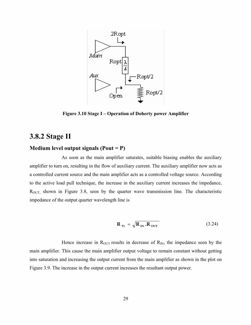
Figure 3.10 Stage I – Operation of Doherty power Amplifier
3.8.2 Stage II Medium level output signals (Pout = P) As soon as the main amplifier saturates, suitable biasing enables the auxiliary
amplifier to turn on, resulting in the flow of auxiliary current. The auxiliary amplifier now acts as
a controlled current source and the main amplifier acts as a controlled voltage source. According
to the active load pull technique, the increase in the auxiliary current increases the impedance,
ROUT, shown in Figure 3.8, seen by the quarter wave transmission line. The characteristic
impedance of the output quarter wavelength line is
(3.24) OUTINTL R.RR =
Hence increase in ROUT results in decrease of RIN, the impedance seen by the
main amplifier. This cause the main amplifier output voltage to remain constant without getting
into saturation and increasing the output current from the main amplifier as shown in the plot on
Figure 3.9. The increase in the output current increases the resultant output power.
29
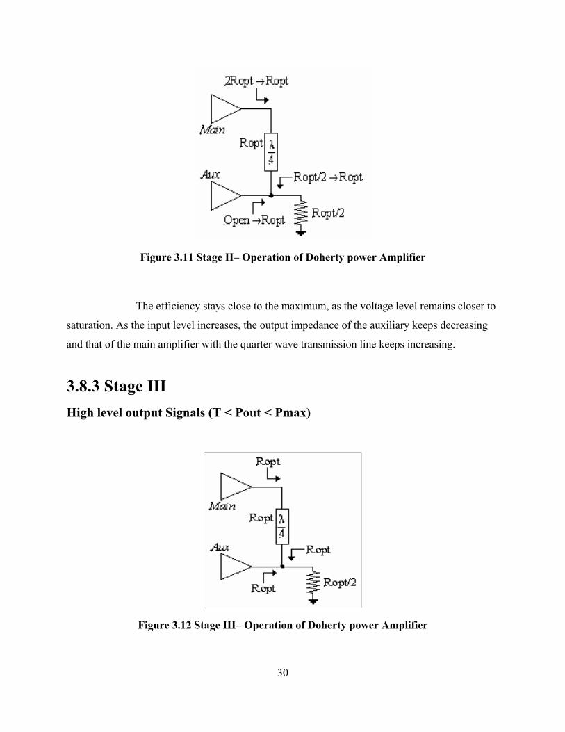
Figure 3.11 Stage II– Operation of Doherty power Amplifier
The efficiency stays close to the maximum, as the voltage level remains closer to
saturation. As the input level increases, the output impedance of the auxiliary keeps decreasing
and that of the main amplifier with the quarter wave transmission line keeps increasing.
3.8.3 Stage III High level output Signals (T < Pout < Pmax)
Figure 3.12 Stage III– Operation of Doherty power Amplifier
30
As the input level increases, the load power keeps increasing until the auxiliary
amplifier saturates. Once the maximum level is reached, both the main and the auxiliary
amplifier see an optimum resistance, Ropt equal to the characteristic impedance of the quarter
wave transmission line as shown in Figure 3.12. The main current reaches the maximum point at
this level and hence the output power delivered by the configuration during this stage is largest.
Thus, the peaking amplifier modulates the load during the signal peaks in order to prevent the
main amplifier from getting into saturation there by maintaining the maximum efficiency.
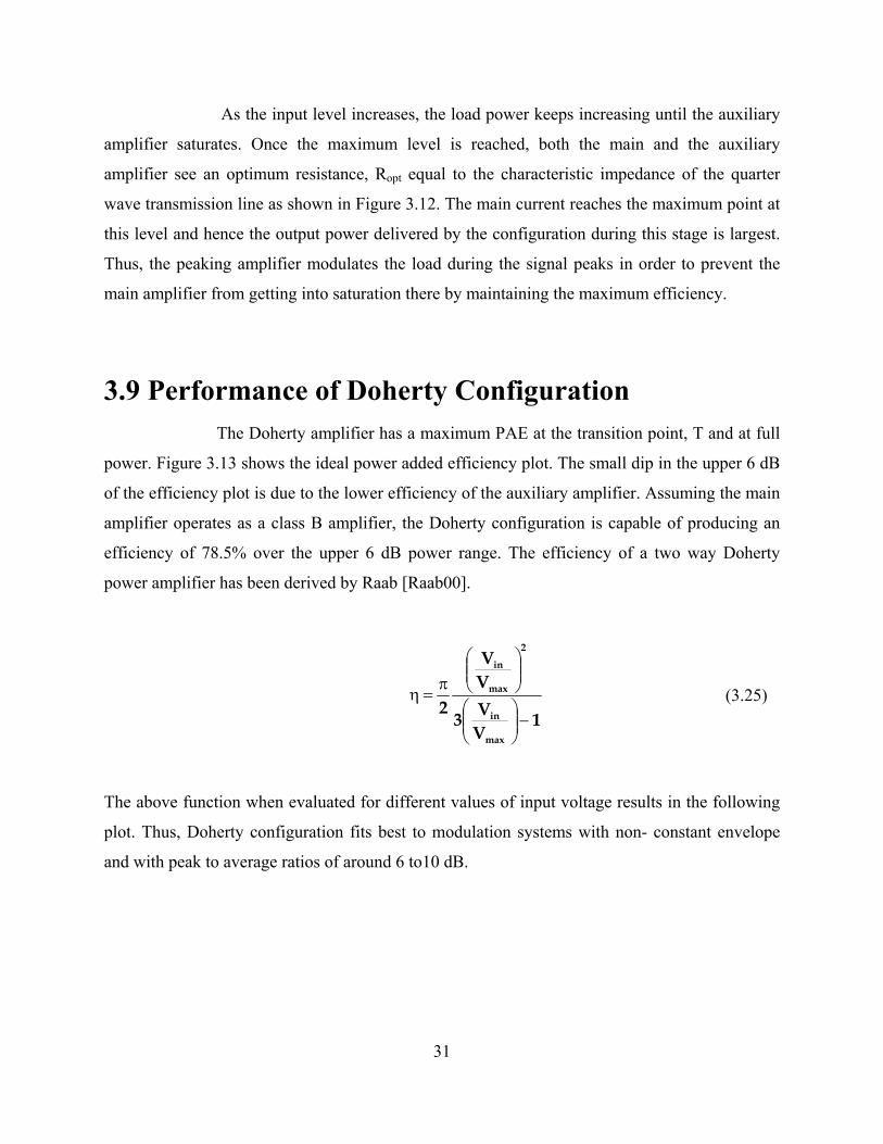
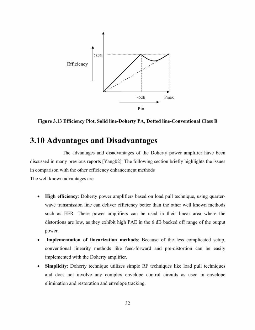
3.9 Performance of Doherty Configuration The Doherty amplifier has a maximum PAE at the transition point, T and at full
power. Figure 3.13 shows the ideal power added efficiency plot. The small dip in the upper 6 dB
of the efficiency plot is due to the lower efficiency of the auxiliary amplifier. Assuming the main
amplifier operates as a class B amplifier, the Doherty configuration is capable of producing an
efficiency of 78.5% over the upper 6 dB power range. The efficiency of a two way Doherty
power amplifier has been derived by Raab [Raab00].
1VV3
VV
2
max
in
2
max
in
−⎟⎟⎠
⎞⎜⎜⎝
⎛
⎟⎟⎠
⎞⎜⎜⎝
⎛
π=η
(3.25)
The above function when evaluated for different values of input voltage results in the following
plot. Thus, Doherty configuration fits best to modulation systems with non- constant envelope
and with peak to average ratios of around 6 to10 dB.
31
78.5%
-6dB
Efficiency
Pmax
Pin
Figure 3.13 Efficiency Plot, Solid line-Doherty PA, Dotted line-Conventional Class B
3.10 Advantages and Disadvantages The advantages and disadvantages of the Doherty power amplifier have been
discussed in many previous reports [Yang02]. The following section briefly highlights the issues
in comparison with the other efficiency enhancement methods
The well known advantages are
• High efficiency: Doherty power amplifiers based on load pull technique, using quarter-
wave transmission line can deliver efficiency better than the other well known methods
such as EER. These power amplifiers can be used in their linear area where the
distortions are low, as they exhibit high PAE in the 6 dB backed off range of the output
power.
• Implementation of linearization methods: Because of the less complicated setup,
conventional linearity methods like feed-forward and pre-distortion can be easily
implemented with the Doherty amplifier.
• Simplicity: Doherty technique utilizes simple RF techniques like load pull techniques
and does not involve any complex envelope control circuits as used in envelope
elimination and restoration and envelope tracking.
32
33
The Doherty configuration also has few disadvantages such as gain degradation,
poor intermodulation distortion and narrow bandwidth. The narrow bandwidth is caused due to
the use of quarter-wave transmission line. Since modern wireless communications utilize a very
narrow bandwidth, this is not a serious drawback. Similar is the gain degradation caused due to
the peaking amplifier. This degradation can be kept low due to the high gain of the carrier
amplifier at low power levels. Another major drawback is the intermodulation distortion, which
is due to the low biasing of the peaking amplifier. A solution to this issue has been suggested
[Iwam00] which involves suitable biasing of the main amplifier leading to the cancellation of the
non-linear products. N- way configuration is also a solution, which will be discussed in depth in
the following chapters. Another well-known issue that can be seen from the configuration of a
Doherty system is the resistive load matching. A Solution has also been published for these
issues [Yang02] where transmission lines with offset have been used to load modulate reactive
termination.
3.11 Conclusion Although ideal behavior of Doherty technique had been explained, the practical
implementation requires main and peaking amplifiers that behave though not exactly, but closer
to the ideal characteristics. Different classes of operation of power amplifier that best matches
the ideal performance of the main and peaking amplifier needs to be optimized for better
efficiency and linearity. The following chapters discuss the performance of different combination
of amplifiers in Doherty configuration and possible methods of improving its performance. A
detailed design procedure and performance analysis of a two way Doherty power amplifier using
LDMOS transistors at 2.14 GHz has been provided and linearity enhancements techniques like
derivation superposition and adaptive bias has been discussed and possible methods of
implementation have been suggested.
34
Chapter 4
Design and Implementation 4.1 Introduction The basic principle and operation of the Doherty topology has been explained in
the previous chapter. This section explains its design and implementation in a detailed manner.
The choice of class of operation of the power amplifier that closely matches the operation of the
main and auxiliary stages of the ideal Doherty power amplifier is analyzed and its performance is
compared with the corresponding conventional power amplifier. This section provides a detailed
design procedure of a two stage Doherty topology and its performance evaluation in the UMTS
band. It features DC simulation, bias point selection, S-parameter simulation, matching circuit
design, load pull characterization and optimization.
4.2 WCDMA Specifications As stated earlier, the goal of this project is to study and realize a Doherty power
amplifier for WCDMA applications. The WCDMA specification is called Universal Mobile
Telecommunications System and was developed by the third generation partnership project
(3GPP). The standard has been introduced to cater specifically to high data rate applications
requiring spectrally efficient modulation scheme. The peak to average ratio depends on the
number of data channels being used. Hence, higher data rates results in very high peak to average
ratio. WCDMA offers variable data rates of up to 2 Mbps. The crest factor (peak-to average
power ratio) is closer to 6 dB, which is higher than even that of QPSK modulation. Base station
power amplifiers operate at a power level reduced from saturation where efficiency is much
lower. This calls for the implementation of an efficiency enhancement topology that would
compensate for the battery loss at backed off power.
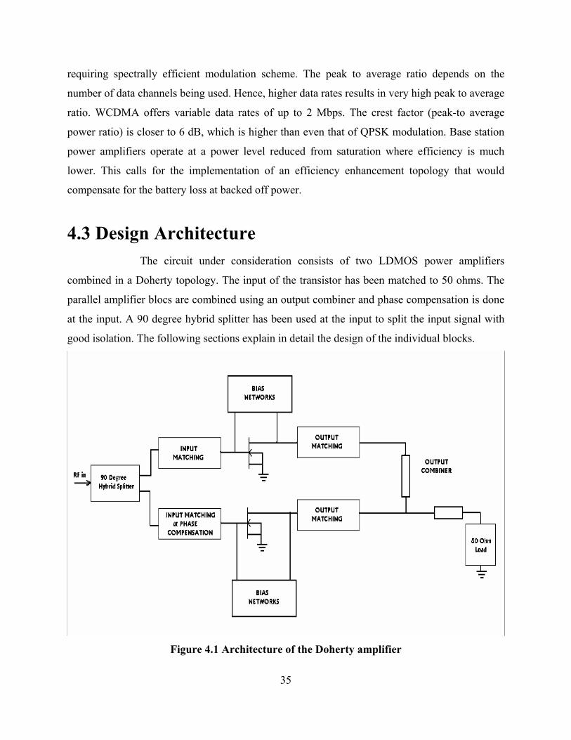
4.3 Design Architecture The circuit under consideration consists of two LDMOS power amplifiers
combined in a Doherty topology. The input of the transistor has been matched to 50 ohms. The
parallel amplifier blocs are combined using an output combiner and phase compensation is done
at the input. A 90 degree hybrid splitter has been used at the input to split the input signal with
good isolation. The following sections explain in detail the design of the individual blocks.
Figure 4.1 Architecture of the Doherty amplifier
35
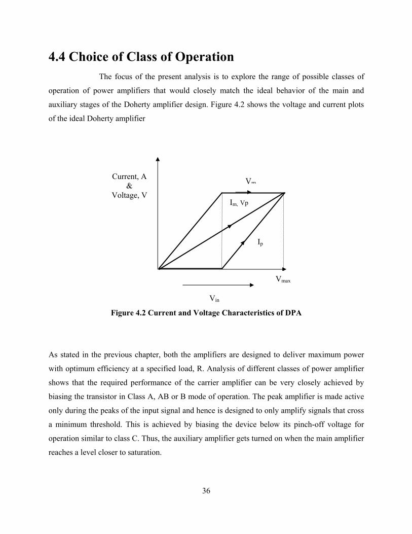
4.4 Choice of Class of Operation The focus of the present analysis is to explore the range of possible classes of
operation of power amplifiers that would closely match the ideal behavior of the main and
auxiliary stages of the Doherty amplifier design. Figure 4.2 shows the voltage and current plots
of the ideal Doherty amplifier
36
Im, Vp
Vm
Vmax
Ip
Current, A &
Voltage, V
Figure 4.2 Current and Voltage Characteristics of DPA
Vin
As stated in the previous chapter, both the amplifiers are designed to deliver maximum power
with optimum efficiency at a specified load, R. Analysis of different classes of power amplifier
shows that the required performance of the carrier amplifier can be very closely achieved by
biasing the transistor in Class A, AB or B mode of operation. The peak amplifier is made active
only during the peaks of the input signal and hence is designed to only amplify signals that cross
a minimum threshold. This is achieved by biasing the device below its pinch-off voltage for
operation similar to class C. Thus, the auxiliary amplifier gets turned on when the main amplifier
reaches a level closer to saturation.
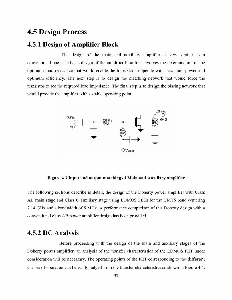
4.5 Design Process 4.5.1 Design of Amplifier Block The design of the main and auxiliary amplifier is very similar to a
conventional one. The basic design of the amplifier bloc first involves the determination of the
optimum load resistance that would enable the transistor to operate with maximum power and
optimum efficiency. The next step is to design the matching network that would force the
transistor to see the required load impedance. The final step is to design the biasing network that
would provide the amplifier with a stable operating point.
Figure 4.3 Input and output matching of Main and Auxiliary amplifier
The following sections describe in detail, the design of the Doherty power amplifier with Class
AB main stage and Class C auxiliary stage using LDMOS FETs for the UMTS band centering
2.14 GHz and a bandwidth of 5 MHz. A performance comparison of this Doherty design with a
conventional class AB power amplifier design has been provided.
4.5.2 DC Analysis Before proceeding with the design of the main and auxiliary stages of the
Doherty power amplifier, an analysis of the transfer characteristics of the LDMOS FET under
consideration will be necessary. The operating points of the FET corresponding to the different
classes of operation can be easily judged from the transfer characteristics as shown in Figure 4.4.
37
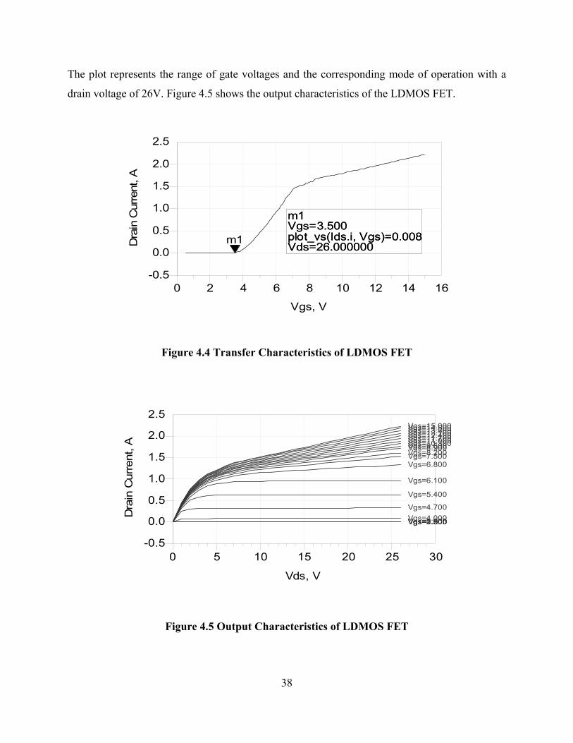
The plot represents the range of gate voltages and the corresponding mode of operation with a
drain voltage of 26V. Figure 4.5 shows the output characteristics of the LDMOS FET.
m1Vgs=plot_vs(Ids.i, Vgs)=0.008Vds=26.000000
3.500m1Vgs=plot_vs(Ids.i, Vgs)=0.008Vds=26.000000
3.500
2 4 6 8 10 12 140 16
0.0
0.5
1.0
1.5
2.0
-0.5
2.5
Vgs, V
Dra
in C
urre
nt, A
m1
Figure 4.4 Transfer Characteristics of LDMOS FET
5 10 15 20 250 30
0.0
0.5
1.0
1.5
2.0
-0.5
2.5
Vgs=0.500Vgs=1.200Vgs=1.900Vgs=2.600Vgs=3.300Vgs=4.000Vgs=4.700
Vgs=5.400
Vgs=6.100
Vgs=6.800Vgs=7.500Vgs=8.200Vgs=8.900Vgs=9.600Vgs=10.300Vgs=11.000Vgs=11.700Vgs=12.400Vgs=13.100Vgs=13.800Vgs=14.500Vgs=15.000
Vds, V
Dra
in C
urre
nt, A
Figure 4.5 Output Characteristics of LDMOS FET
38
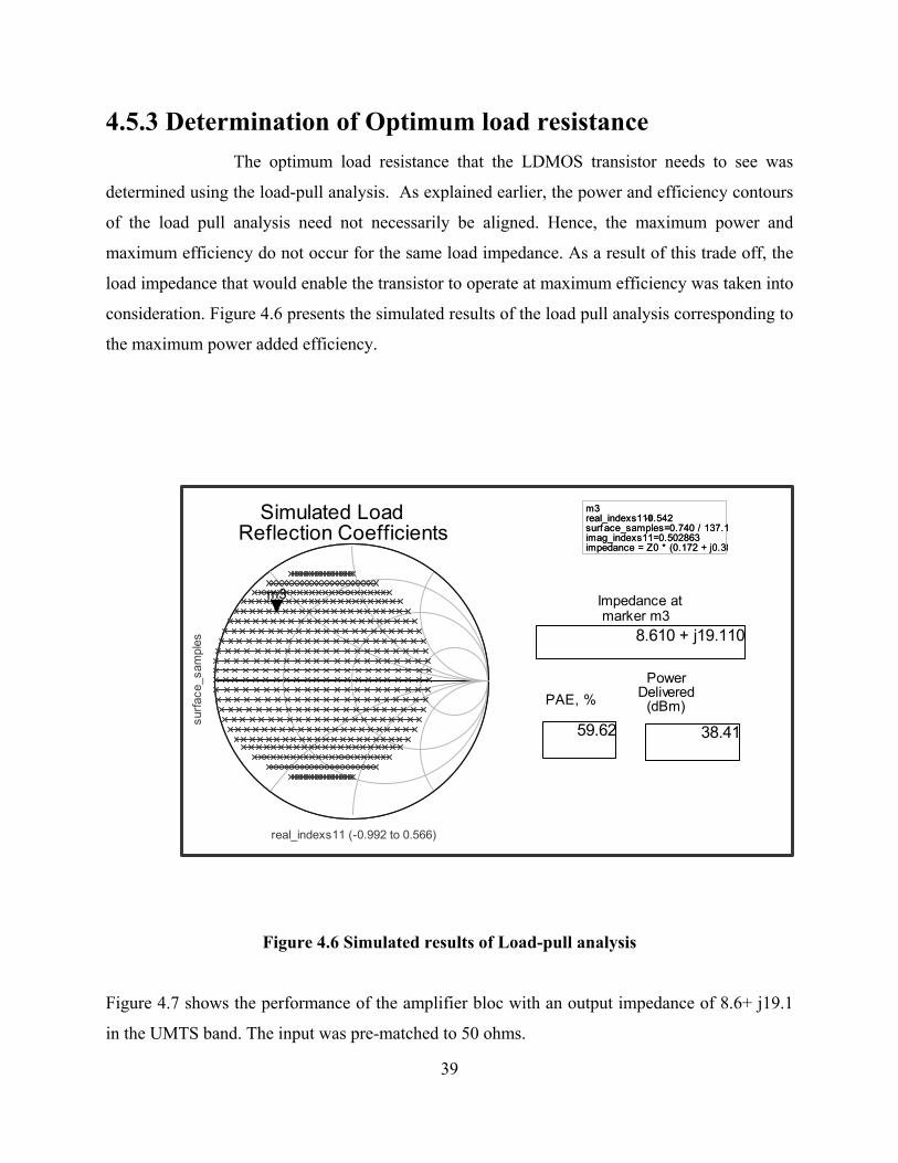
4.5.3 Determination of Optimum load resistance The optimum load resistance that the LDMOS transistor needs to see was
determined using the load-pull analysis. As explained earlier, the power and efficiency contours
of the load pull analysis need not necessarily be aligned. Hence, the maximum power and
maximum efficiency do not occur for the same load impedance. As a result of this trade off, the
load impedance that would enable the transistor to operate at maximum efficiency was taken into
consideration. Figure 4.6 presents the simulated results of the load pull analysis corresponding to
the maximum power added efficiency.
m3real_indexs11=surf ace_samples=0.740 / 137.1imag_indexs11=0.502863impedance = Z0 * (0.172 + j0.38
-0.542m3real_indexs11=surf ace_samples=0.740 / 137.1imag_indexs11=0.502863impedance = Z0 * (0.172 + j0.38
-0.542
real_indexs11 (-0.992 to 0.566)
surfa
ce_s
ampl
es
m3
59.62
PAE, %
8.610 + j19.110
Impedance at marker m3
38.41
Power Delivered (dBm)
Simulated Load Reflection Coefficients
Figure 4.6 Simulated results of Load-pull analysis
Figure 4.7 shows the performance of the amplifier bloc with an output impedance of 8.6+ j19.1
in the UMTS band. The input was pre-matched to 50 ohms.
39
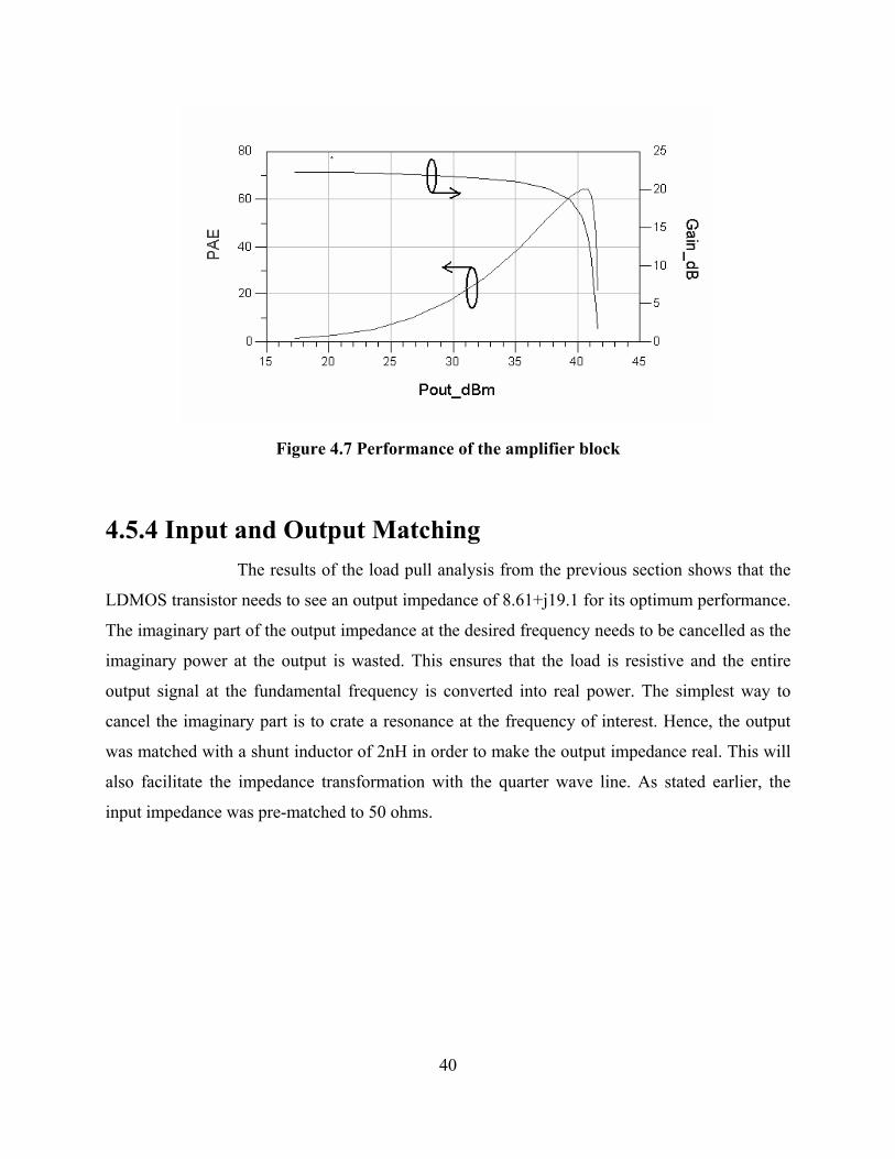
Figure 4.7 Performance of the amplifier block
4.5.4 Input and Output Matching The results of the load pull analysis from the previous section shows that the
LDMOS transistor needs to see an output impedance of 8.61+j19.1 for its optimum performance.
The imaginary part of the output impedance at the desired frequency needs to be cancelled as the
imaginary power at the output is wasted. This ensures that the load is resistive and the entire
output signal at the fundamental frequency is converted into real power. The simplest way to
cancel the imaginary part is to crate a resonance at the frequency of interest. Hence, the output
was matched with a shunt inductor of 2nH in order to make the output impedance real. This will
also facilitate the impedance transformation with the quarter wave line. As stated earlier, the
input impedance was pre-matched to 50 ohms.
40
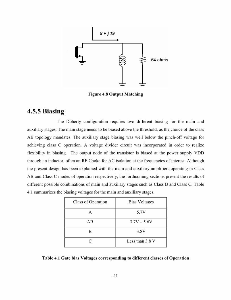
Figure 4.8 Output Matching
4.5.5 Biasing The Doherty configuration requires two different biasing for the main and
auxiliary stages. The main stage needs to be biased above the threshold, as the choice of the class
AB topology mandates. The auxiliary stage biasing was well below the pinch-off voltage for
achieving class C operation. A voltage divider circuit was incorporated in order to realize
flexibility in biasing. The output node of the transistor is biased at the power supply VDD
through an inductor, often an RF Choke for AC isolation at the frequencies of interest. Although
the present design has been explained with the main and auxiliary amplifiers operating in Class
AB and Class C modes of operation respectively, the forthcoming sections present the results of
different possible combinations of main and auxiliary stages such as Class B and Class C. Table
4.1 summarizes the biasing voltages for the main and auxiliary stages.
Class of Operation Bias Voltages A 5.7V
AB 3.7V – 5.6V
B 3.8V
C Less than 3.8 V
Table 4.1 Gate bias Voltages corresponding to different classes of Operation
41

4.5.6 Design of output combiner The topology used of the output combiner is the quarter-wave
impedance transformer. Figure 4.9 shows the output circuit constitution with an added
impedance transformer. The output combiner is designed as per the Doherty technique explained
in the previous chapter. As explained with a load-pull analysis, an output impedance of 64 Ohms
in front of the quarter-wave transformer allows the main amplifier to have an optimum
performance. The value of RL is determined by the number of amplifier blocks in parallel N, and
the value of output impedance to be presented at the output of the amplifier block for having its
optimum performances.
N
RR OPT
L = (4.1)
For a design of a 2-way Doherty amplifier,
2OPT
LR
R = (4.2)
For an output impedance of 64 ohms,
Ω== 322
64LR (4.3)
For a 2 way configuration, R1 is same as Ropt
R1 = 64Ω (4.4)
42
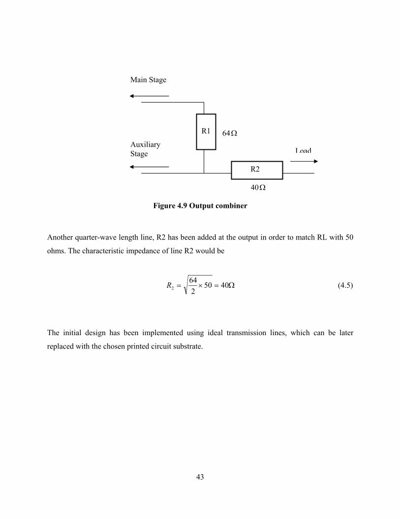
Main Stage
64Ω
R1
R2
Auxiliary Stage
40Ω
Figure 4.9 Output combiner
Another quarter-wave length line, R2 has been added at the output in order to
ohms. The characteristic impedance of line R2 would be
Ω=×= 40502
642R
The initial design has been implemented using ideal transmission lines, w
replaced with the chosen printed circuit substrate.
43
Load
match RL with 50
(4.5)
hich can be later
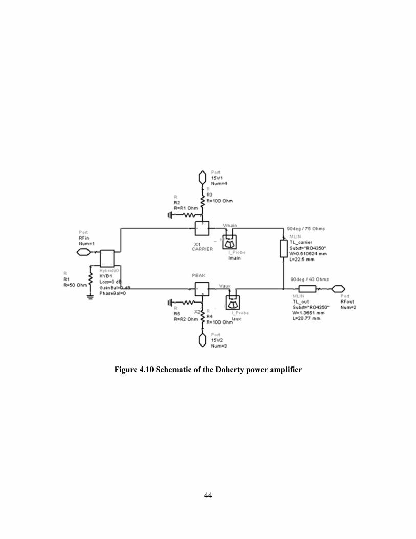
Figure 4.10 Schematic of the Doherty power amplifier
44
45
4.6 Implementation Figure 4.10 shows the schematic diagram of the Doherty amplifier with the
parallel combination of main and auxiliary amplifier blocs. Identical devices (LDMOS FETs) are
used for the design of both carrier and peaking amplifiers. The output of both the main and
auxiliary amplifier is matched to 64 ohms to have a load impedance of 8.61 + j19.1. A 64 ohm
quarter-wave length line is used for a load-pull operation and a 40 ohm quarter-wave length line
is used for matching the combined two 64 ohm lines to 50 ohms. The input signal is split into
two quadrature (90 degrees phase difference) components by the hybrid divider. These two
signal components are applied to two stages, the main and auxiliary, which are identical except
for their gate bias levels. The main is connected to the in-phase (0 degree) and the auxiliary is
connected to the quadrature (-90 degrees) output. This compensates for the phase mismatch
caused due to the quarter-wave line at the output of the main stage. The biasing of the individual
stages can be done by choosing appropriate resistor values for the voltage divider.
4.7 Conclusion The complete schematic of the two stage Doherty power amplifier for the UMTS
band has been implemented. The performance of the Doherty topology depends mainly on the
class of operation of the two amplifier blocs. There are numerous possible ways of combinations
and every design has its own trade off with another. The following chapter presents an analysis
of possible combinations of the main and auxiliary stages and optimization of the simulation
results.
46
Chapter 5
Simulation and Results
5.1 Introduction
The performance analysis of the designed Doherty topology was done using
Agilent’s Advanced Design System 2003. The chapter provides the single tone and two tone
simulation results of two different realizations of Doherty Power amplifiers. Both the designs
have been compared with the corresponding conventional power amplifiers. The chapter also
provides the effects of biasing on the main and auxiliary stages in order to optimize the design
with the best efficiency versus linearity characteristics. Finally, a literary study has been
furnished on the possible methods of improving the linearity performance of the Doherty
topology.
5.2 Doherty amplifier I Doherty amplifier I is a combination of Class AB main stage and Class C
auxiliary stage. The bias points were set based on the transfer characteristics of the LDMOS
transistors used, as presented in Figure 4.4. Table 5.1 shows the chosen bias point, as there could
be a range of possible operating points for the operation of both class AB and class C.
Class of
Operation
Main stage
Class AB
Auxiliary Stage
Class C
Gate Voltage 3.80 3.00
Table 5.1 Doherty amplifier I Bias points
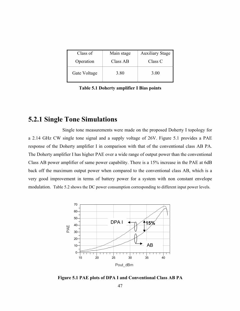
5.2.1 Single Tone Simulations Single tone measurements were made on the proposed Doherty I topology for
a 2.14 GHz CW single tone signal and a supply voltage of 26V. Figure 5.1 provides a PAE
response of the Doherty amplifier I in comparison with that of the conventional class AB PA.
The Doherty amplifier I has higher PAE over a wide range of output power than the conventional
Class AB power amplifier of same power capability. There is a 15% increase in the PAE at 6dB
back off the maximum output power when compared to the conventional class AB, which is a
very good improvement in terms of battery power for a system with non constant envelope
modulation. Table 5.2 shows the DC power consumption corresponding to different input power levels.
20 25 3015
10
20
30
40
50
60
0
70
Pout_dBm
PA
E
%
Figure 5.1 PAE plots of DPA I and Conven
47
15
t
AB
DPA I
35 40
ional Class AB PA
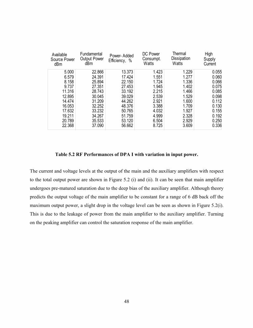
5.0006.5798.1589.737
11.31612.89514.47416.05317.63219.21120.78922.368
22.86624.39125.89427.35128.74330.04531.20932.25233.23234.26735.53337.090
13.37317.42422.15027.45333.19239.02944.26248.37650.76551.75953.12056.662
1.4231.5511.7241.9452.2152.5392.9213.3884.0324.9996.5048.725
1.2291.2771.3361.4021.4661.5291.6001.7091.9272.3282.9293.609
0.0550.0600.0660.0750.0850.0980.1120.1300.1550.1920.2500.336
HighSupply Current
ThermalDissipation Watts
DC PowerConsumpt. Watts
Available Source Power dBm
FundamentalOutput Power dBm
Power- AddedEfficiency, %
Table 5.2 RF Performances of DPA I with variation in input power.
The current and voltage levels at the output of the main and the auxiliary amplifiers with respect
to the total output power are shown in Figure 5.2 (i) and (ii). It can be seen that main amplifier
undergoes pre-matured saturation due to the deep bias of the auxiliary amplifier. Although theory
predicts the output voltage of the main amplifier to be constant for a range of 6 dB back off the
maximum output power, a slight drop in the voltage level can be seen as shown in Figure 5.2(i).
This is due to the leakage of power from the main amplifier to the auxiliary amplifier. Turning
on the peaking amplifier can control the saturation response of the main amplifier.
48
6 dB
Figure 5.2(i) Voltage variations of main and auxiliary stage for DPA I
49
Figure 5.2(ii) Current variations of main and auxiliary stage for DPA I
The drain current waveforms of the main and the auxiliary amplifier are shown in Figure 5.3.
Although this does not clearly indicate the class of operation assumed, it was considered
insignificant as the current levels of the main and auxiliary amplifier, as shown in Figure 5.2(ii)
agrees with the Doherty principle.
6 dB
20 25 30 3515 40
0.10
0.20
0.30
0.40
0.00
0.45
Output Power, dBm
Cur
rent
, A
Auxiliary
Main
0.1 0.2 0.3 0.4 0.5 0.6 0.7 0.8 0.90.0 1.0
0
1
2
-1
3
time, nsec
ts(Ia
ux.i)
, A
0.1 0.2 0.3 0.4 0.5 0.6 0.7 0.8 0.90.0 1.0
0
1
2
-1
3
time, nsec
ts(Im
ain.
i), A
Figure 5.3 Drain current waveforms of main and auxiliary stage of DPA I
Figure 5.4 shows the gain plots of the Doherty amplifier I and conventional Class AB PA.
Although the gain shape and P1dB are similar, there is a slight drop in the gain as compared to
the conventional one. Since the auxiliary amplifier is biased in class C, it is typically difficult to
match the gain of this amplifier to be greater than the main amplifier unless the overall gain is
sacrificed. This situation could be overcome by delivering higher power to the auxiliary
amplifier than the main amplifier [Iwam00].
CLASS AB
15 20 25 30 35 4010 45
5
10
15
0
20
Pout_dBm
Gai
n_dB
DPA I
Figure 5.4 Gain of DPA I and Conventional Class AB
50
Figure 5.5 gives the measured return-loss performance of DPA I. The input return loss is greater
than 13 dB across the entire range of input power.
10 15 20 25 30 35 405 45
-30
-25
-20
-15
-35
-10
Output Power, dBm
Ret
urn
Loss
, dB
Figure 5.5 Input return loss (dB) of DPA I
5.2.2 Two Tone Simulations Two tone simulations were performed with a center frequency of 2.14 GHz
and a tone spacing of 1MHz. The simulated IMD3 and IMD5 response of the proposed topology
as a function of the input power have been provided in Figure5.6 (i) and (ii).
m3Pout_dBm=plot_vs(IMD3, Pout_dBm)=-15.143
38.438
m4Pout_dBm=plot_vs(IMD3, Pout_dBm)=-28.917
27.302
15 20 25 30 3510 40
-50
-40
-30
-20
-60
-10
Output Power, dBm
IMD
3 (d
Bc)
m3
m4
Figure 5.6(i) IMD3 (dBc) of DPA I for a two-tone signal
51
m3Pout_dBm=plot_vs(IMD5, Pout_dBm)=-35.167
32.985
19 24 29 3414 39
-70
-60
-50
-40
-30
-20
-80
-10
Output power, dBm
IMD
5 (d
Bc) m3
Figure 5.6(ii) IMD5 (dBc) of DPA I for a two-tone signal
Figure 5.7 shows the IMD3 distortion power of the conventional class AB and Doherty PA with
the variation in the output power. It can be seen that the Doherty topology has a poor
intermodulation distortion performance. This is due to the low biasing conditions of the peaking
amplifiers, which cause distortions. The bias optimization is very important for proper
cancellation of the intermodulation terms generated by the carrier and the auxiliary amplifier.
m3Pout_dBm=plot_vs(IMD3, Pout_dBm)=-15.800
38.396
m4Pout_dBm=plot_vs(IMD3, Pout_dBm)=-36.939
26.284
15 20 25 30 3510 40
-50
-40
-30
-20
-60
-10
Output Power, dBm
IMD
3 (d
Bc)
m3
m4
DPA I
Class AB
Figure 5.7 IMD3 Comparison of DPA I and Conventional Class AB for a two-tone signal
52
53
T
power amplifier and the proposed Doherty I power amplifier. The proposed Doherty topology
Conventional Class AB
Doherty PA
I
able 5.3 summarizes the comparison of performances between the conventional class AB
shows improvement in PAE response without any appreciable change in other RF characteristics
in comparison with a class AB PA design.
Supply Voltage, V 26 2 6Drain Current, mA 90 98 Gain @ 2.14 GHz 18.5 17 IMD3 dBm @ Pout = 20dBm -48 -45 Output IP3 (dBm) 44 41
Table 5.3 RF responses of DPA I and Class AB power amplifier
.3 Doherty II (Class B + Class C) onse of Doherty I topology was
e was an obvious choice. Doherty
Table 5.4 Doherty amplifier II Bias points
Class of
Operation
Main stage
Class B
Auxiliary Stage
Class C
5 The possibility of improving the PAE resp
investigated and adapting a class B operation for the main stag
amplifier II is a parallel combination of class B and Class C amplifiers. The design procedure is
very similar to that of Doherty I amplifier Table 5.4 summarizes the biasing voltages for the
main and auxiliary stages. It can be noted that a deeper class C bias of 2.3V was used for the
auxiliary stage of DPA II.
Gate Voltage 3.60 V 2.30 V
54
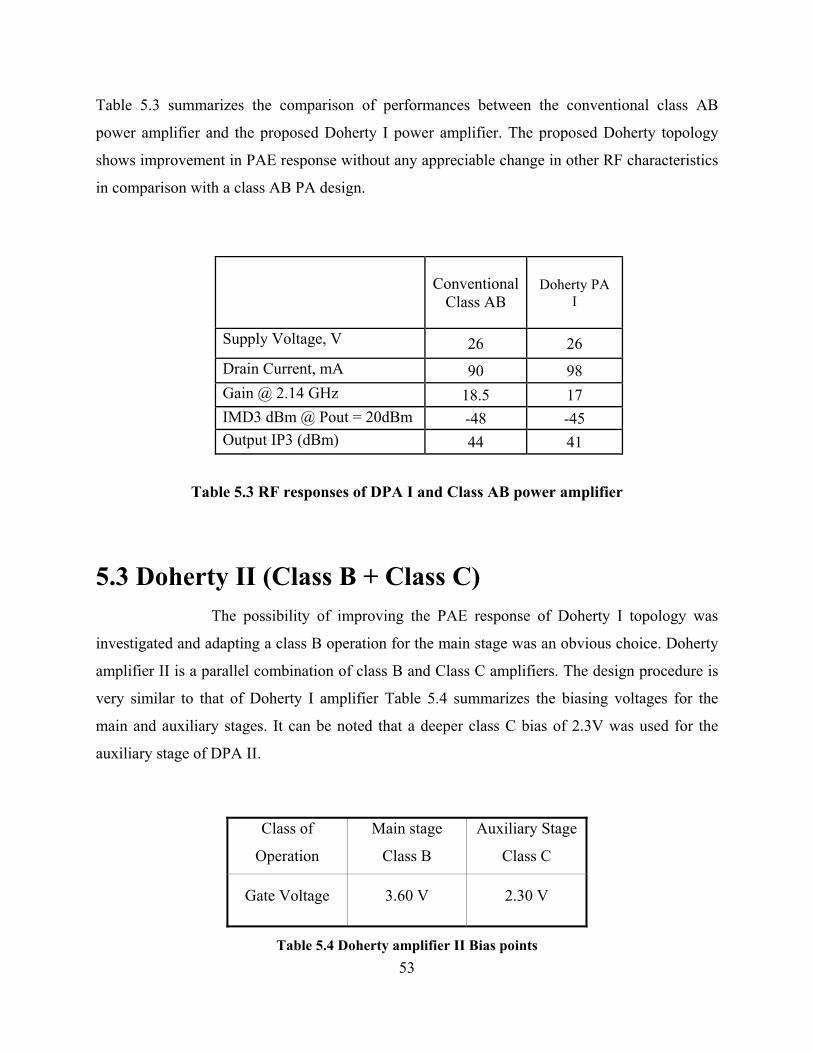
nlike DPA I, the PAE re DPA I otic back off power. It is
epicted by ‘m2’ in Figu is initia PAE at 5 urs at an output power of
4 dBm. The P1dB is a a PAE . Though r reason for this behavior
the class B bias of the main stage, the deeper bias of the auxiliary stage also plays a significant
role. The bias level of the saturation response of the
main amplifier.
U sponse of
re 5.8(i). Th
I exhibits a n eable peak at the
d l peak in 4.8% occ
3 t 40 dBm with of 68% the majo
is
auxiliary stage was optimized for a better
m1Pout_dBm=plot_vs(PAE, Pout_dBm)=68.075
40.254
m2Pout_dBm= 34.028plot_vs(PAE, Pout_dBm)=54.800
10 15 20 25 30 35 405 45
20
40
60
80
0
Pout_dBm
PA
E
m1
m2
Figure 5.8(i) PAE response of Doherty II PA for a single tone signal.
10 15 20 25 30 35 405 45
5
10
15
0
20
Output Power, dBm
Gai
n, d
B
Figure 5.8(ii) Gain response of Doherty II PA for a single tone signal.
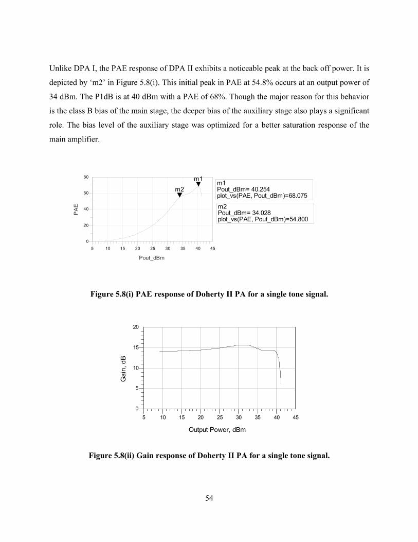
55
As seen in Figure 5.8(ii), the linearity of the gain response deteriorates due to the generation of
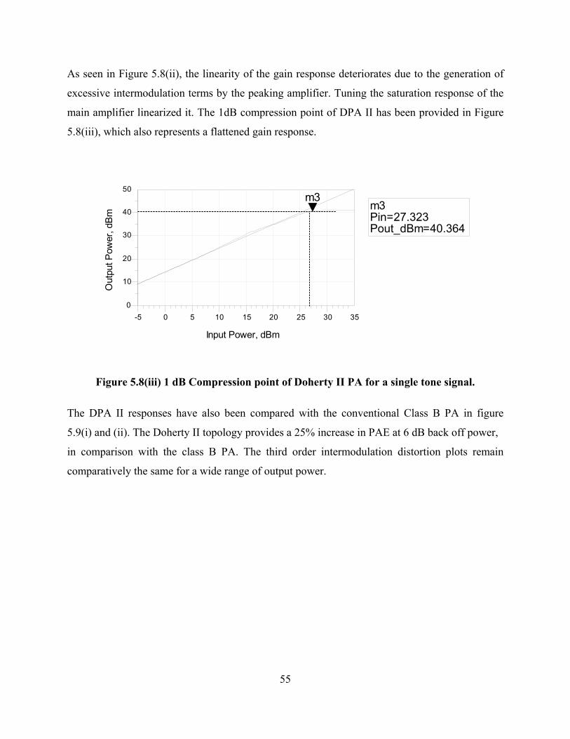
excessive intermodulation terms by the peaking amplifier. Tuning the saturation response of the
main amplifier linearized it. The 1dB compression point of DPA II has been provided in Figure
5.8(iii), which also represents a flattened gain response.
m3Pin=Pout_dBm=40.364
27.323
20
30
40
50
10
0 5 10 15 20 25 30-5 350
Input Power, dBm
Out
put P
ower
, dB
m
m3
Figure 5.8(iii) 1 dB Compression point of Doherty II PA for a single tone signal.
The DPA II responses have also been compared with the conventional Class B PA in figure
5.9(i) and (ii). The Doherty II topology provides a 25% increase in PAE at 6 dB back off power,
in comparison with the class B PA. The third order intermodulation distortion plots remain
comparatively the same for a wide range of output power.
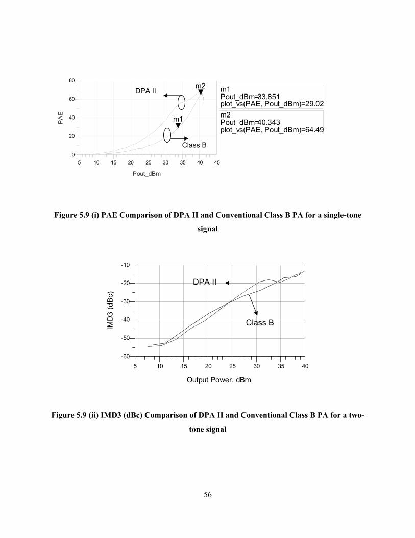
56
o-
Bm=plot_v PAE, Pout_dBm)=29.02
33.851
Figure 5.9 (i) PAE Comparison of DPA II and Conventional Class B PA for a single-tone
signal
Figure 5.9 (ii) IMD3 (dBc) Comparison of DPA II and Conventional Class B PA for a tw
tone signal
m1Pout_d
s(m2Pout_dBm=plot_vs(PAE, Pout_dBm)=64.496
40.343
10 15 20 30 35 405 45
20
40
0
60
80
25
Pout_dBm
PA
E
m1
m2DPA II
Class B
10 15 20 25 30 355 40
-50
-40
-30
-60
-10
-20
Output Power, dBm
IMD
3 (d
Bc
DPA II
Class B
)
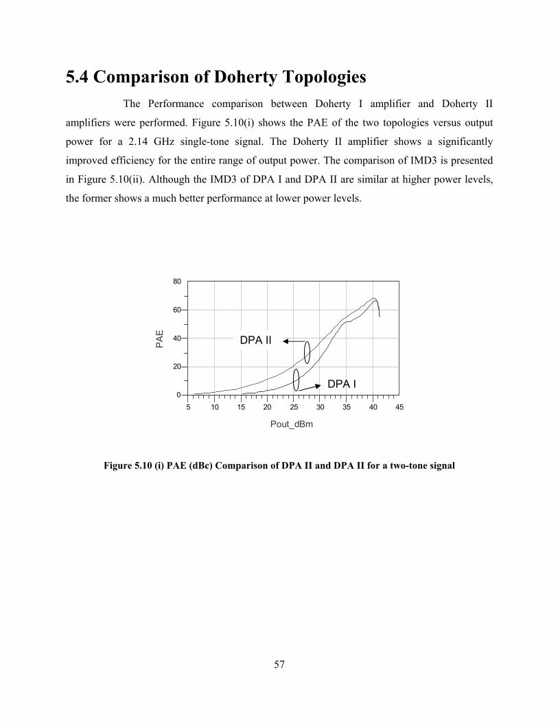
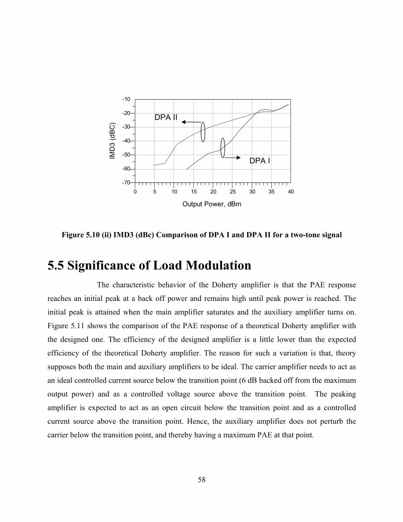
5.4 Comparison of Doherty Topologies
57
The Performance comparison between Doherty I amplifier and Doherty II
plifiers were performed. Figure 5.10(i) shows the PAE of the two topologies versus output
wer for a 2.14 GHz single-tone signal. The Doherty II amplifier shows a significantly
rison of IMD3 is presented
in Figure 5.10(ii). Although the IMD3 of DPA I and DPA II are similar at higher power levels,
am
po
improved efficiency for the entire range of output power. The compa
the former shows a much better performance at lower power levels.
10 15 20 25 30 35 405 45
20
40
60
0
80
Pout_dBm
PA
E
DPA I
DPA II
Figure 5.10 (i) PAE (dBc) Comparison of DPA II and DPA II for a two-tone signal
5 10 15 20 25 30 350 40
-60
-50
-40
-30
-20
-70
-10
Output Power, dBm
IMD
3 (d
BC)
DPA I
DPA II
58
o-tone signal
The E response
reac he
itial peak is attained when the main amplifier saturates and the auxiliary amplifier turns on.
retical Doherty amplifier with
ted
Figure 5.10 (ii) IMD3 (dBc) Comparison of DPA I and DPA II for a tw
5.5 Significance of Load Modulation characteristic behavior of the Doherty amplifier is that the PA
hes an initial peak at a back off power and remains high until peak power is reached. T
in
Figure 5.11 shows the comparison of the PAE response of a theo
the designed one. The efficiency of the designed amplifier is a little lower than the expec
efficiency of the theoretical Doherty amplifier. The reason for such a variation is that, theory
supposes both the main and auxiliary amplifiers to be ideal. The carrier amplifier needs to act as
an ideal controlled current source below the transition point (6 dB backed off from the maximum
output power) and as a controlled voltage source above the transition point. The peaking
amplifier is expected to act as an open circuit below the transition point and as a controlled
current source above the transition point. Hence, the auxiliary amplifier does not perturb the
carrier below the transition point, and thereby having a maximum PAE at that point.
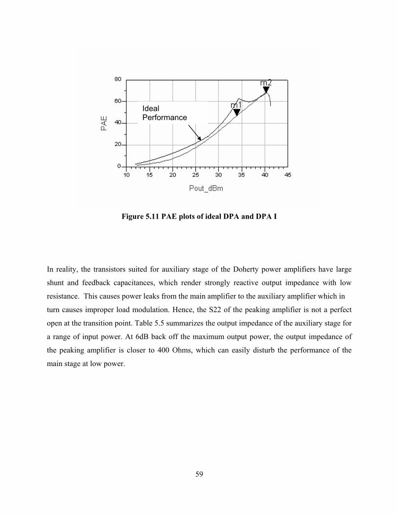
Figure 5.11 PAE plots of ideal DPA and DPA I
Ideal Performance
59
reality, the transistors suited for auxiliary stage of the Doherty power amplifiers have large
hunt and feedback capacitances, which render strongly reactive output impedance with low
sistance. This causes power leaks from the main amplifier to the auxiliary amplifier which in
In
s
re
turn causes improper load modulation. Hence, the S22 of the peaking amplifier is not a perfect
open at the transition point. Table 5.5 summarizes the output impedance of the auxiliary stage for
a range of input power. At 6dB back off the maximum output power, the output impedance of
the peaking amplifier is closer to 400 Ohms, which can easily disturb the performance of the
main stage at low power.
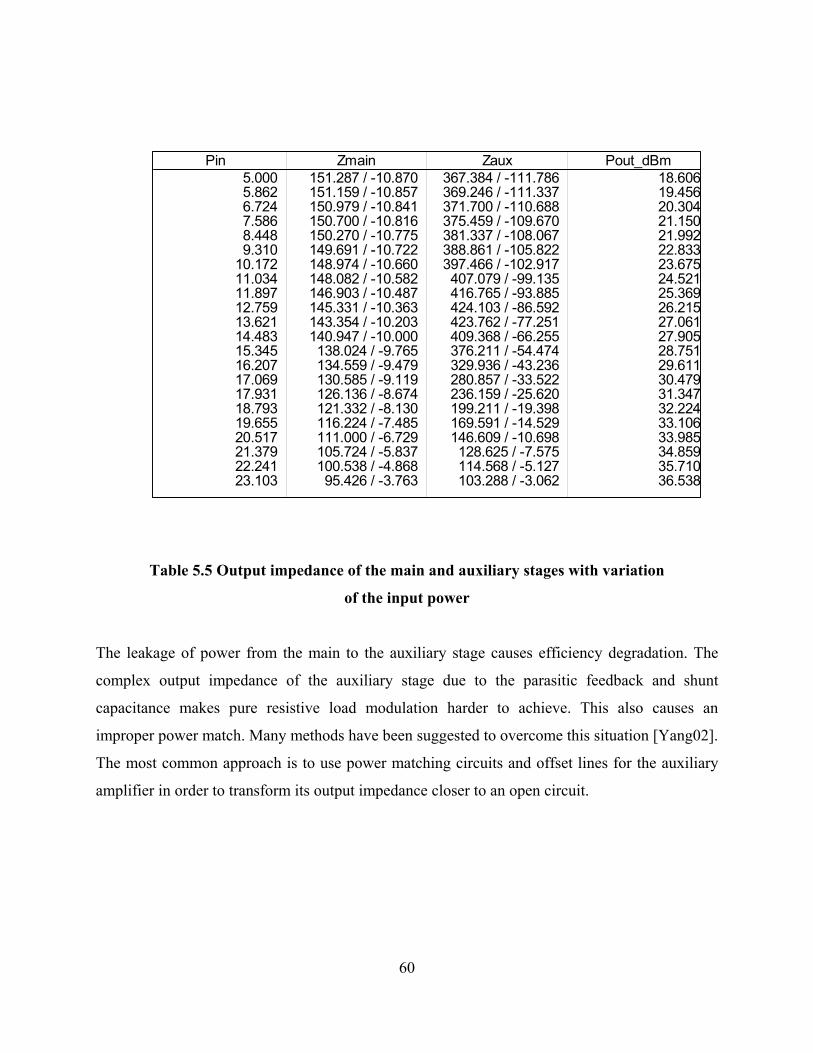
Pin5.0005.8626.7247.5868.4489.310
10.17211.03411.89712.75913.62114.48315.34516.20717.06917.93118.79319.65520.51721.37922.24123.103
Zmain151.287 / -10.870151.159 / -10.857150.979 / -10.841150.700 / -10.816150.270 / -10.775149.691 / -10.722148.974 / -10.660148.082 / -10.582146.903 / -10.487145.331 / -10.363143.354 / -10.203140.947 / -10.000138.024 / -9.765134.559 / -9.479130.585 / -9.119126.136 / -8.674121.332 / -8.130116.224 / -7.485111.000 / -6.729105.724 / -5.837100.538 / -4.86895.426 / -3.763
Zaux367.384 / -111.786369.246 / -111.337371.700 / -110.688375.459 / -109.670381.337 / -108.067388.861 / -105.822397.466 / -102.917407.079 / -99.135416.765 / -93.885424.103 / -86.592423.762 / -77.251409.368 / -66.255376.211 / -54.474329.936 / -43.236280.857 / -33.522236.159 / -25.620199.211 / -19.398169.591 / -14.529146.609 / -10.698128.625 / -7.575114.568 / -5.127103.288 / -3.062
Pout_dBm18.60619.45620.30421.15021.99222.83323.67524.52125.36926.21527.06127.90528.75129.61130.47931.34732.22433.10633.98534.85935.71036.538
Table 5.5 Output impedance of the main and auxiliary stages with variation
of the input power
The leakage of power from the main to the auxiliary stage causes efficiency degradation. The
complex output impedance of the auxiliary stage due to the parasitic feedback and shunt
capacitance makes pure resistive load modulation harder to achieve. This also causes an
improper power match. Many methods have been suggested to overcome this situation [Yang02].
The most common approach is to use power matching circuits and offset lines for the auxiliary
amplifier in order to transform its output impedance closer to an open circuit.
60
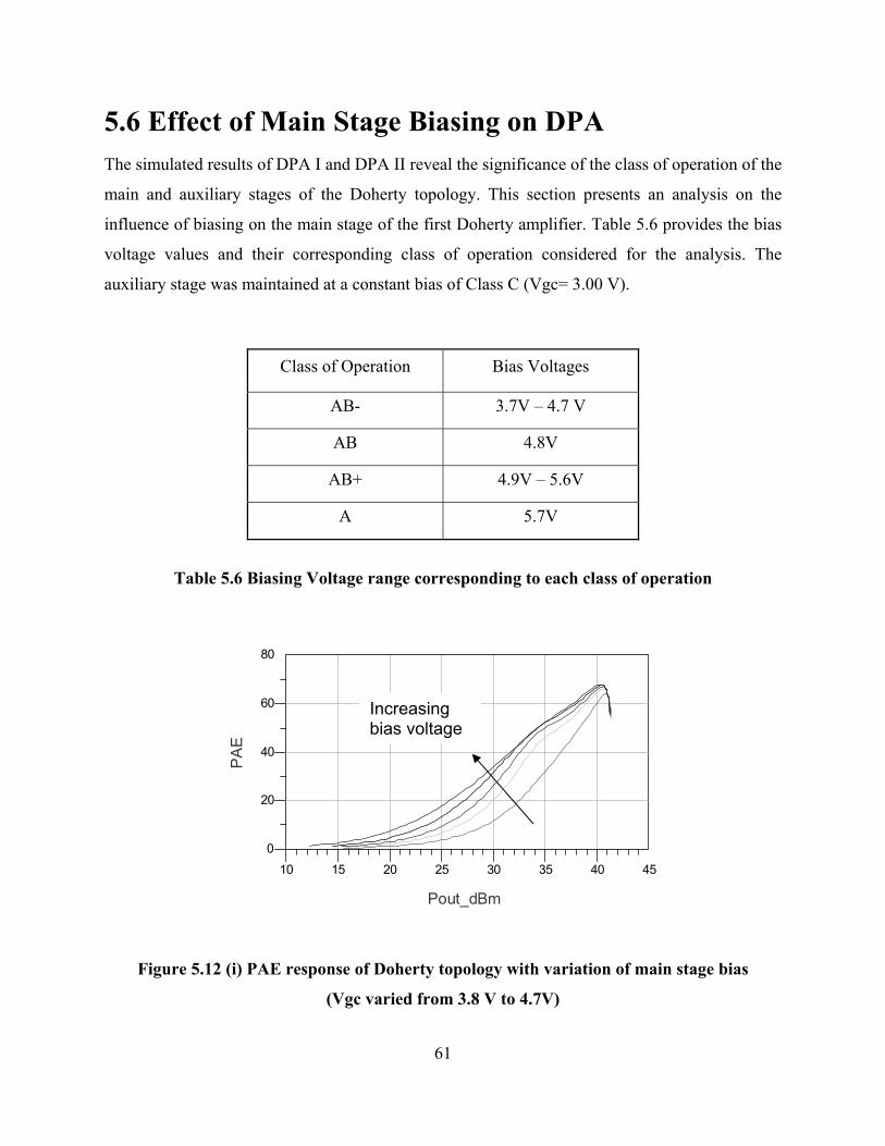
5.6 Effect of Main Stage Biasing on DPA The simulated results of DPA I and DPA II reveal the significance of the class of operation of the
main and auxiliary stages of the Doherty topology. This section presents an analysis on the
influence of biasing on the main stage of the first Doherty amplifier. Table 5.6 provides the bias
voltage values and their corresponding class of operation considered for the analysis. The
auxiliary stage was maintained at a constant bias of Class C (Vgc= 3.00 V).
Class of Operation Bias Voltages AB- 3.7V – 4.7 V
AB 4.8V
AB+ 4.9V – 5.6V
A 5.7V
Table 5.6 Biasing Voltage range corresponding to each class of operation
15 20 25 30 35 4010 45
20
40
60
0
80
Pout_dBm
PA
E
Increasing bias voltage
Figure 5.12 (i) PAE response of Doherty topology with variation of main stage bias
(Vgc varied from 3.8 V to 4.7V)
61
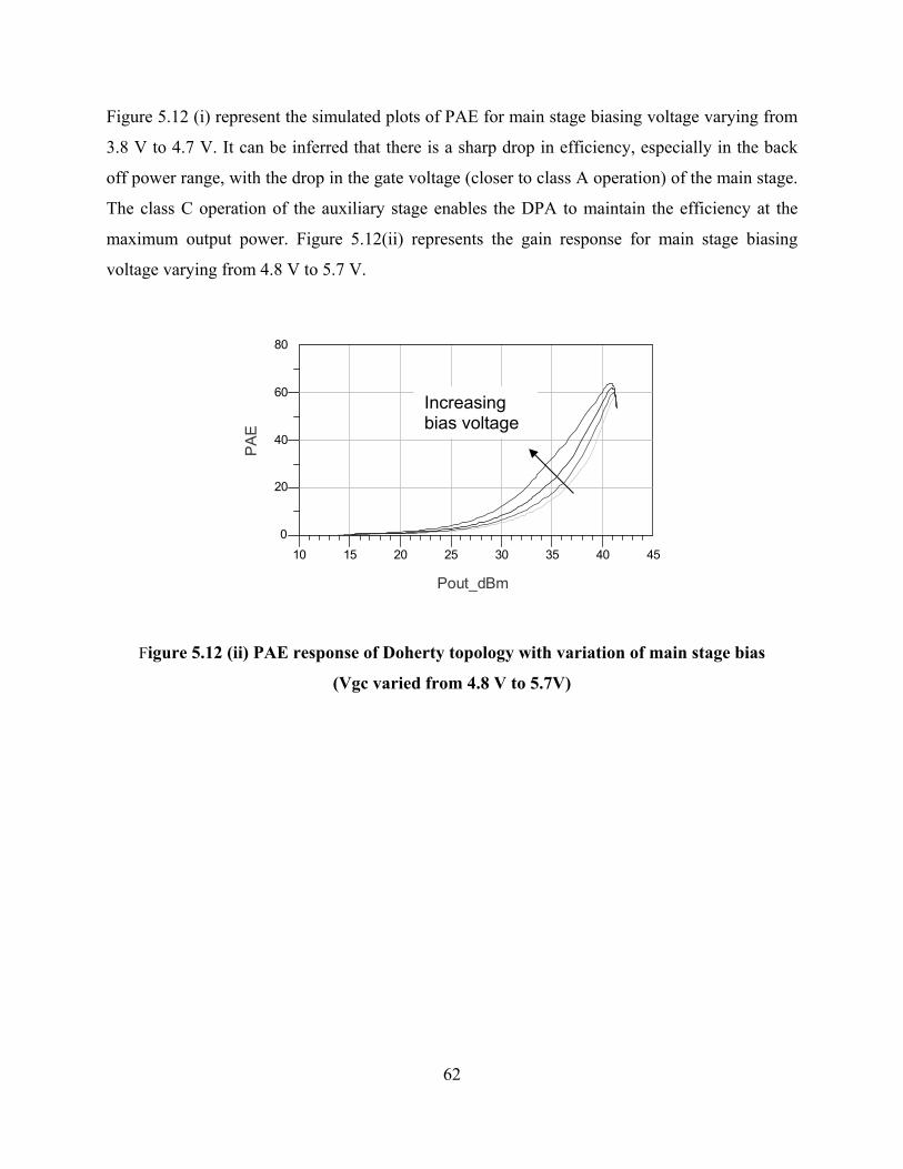
Figure 5.12 (i) represent the simulated plots of PAE for main stage biasing voltage varying from
3.8 V to 4.7 V. It can be inferred that there is a sharp drop in efficiency, especially in the back
off power range, with the drop in the gate voltage (closer to class A operation) of the main stage.
The class C operation of the auxiliary stage enables the DPA to maintain the efficiency at the
maximum output power. Figure 5.12(ii) represents the gain response for main stage biasing
voltage varying from 4.8 V to 5.7 V.
15 20 25 30 35 4010 45
20
40
60
0
80
Pout_dBm
PAE
Increasing bias voltage
Figure 5.12 (ii) PAE response of Doherty topology with variation of main stage bias
(Vgc varied from 4.8 V to 5.7V)
62
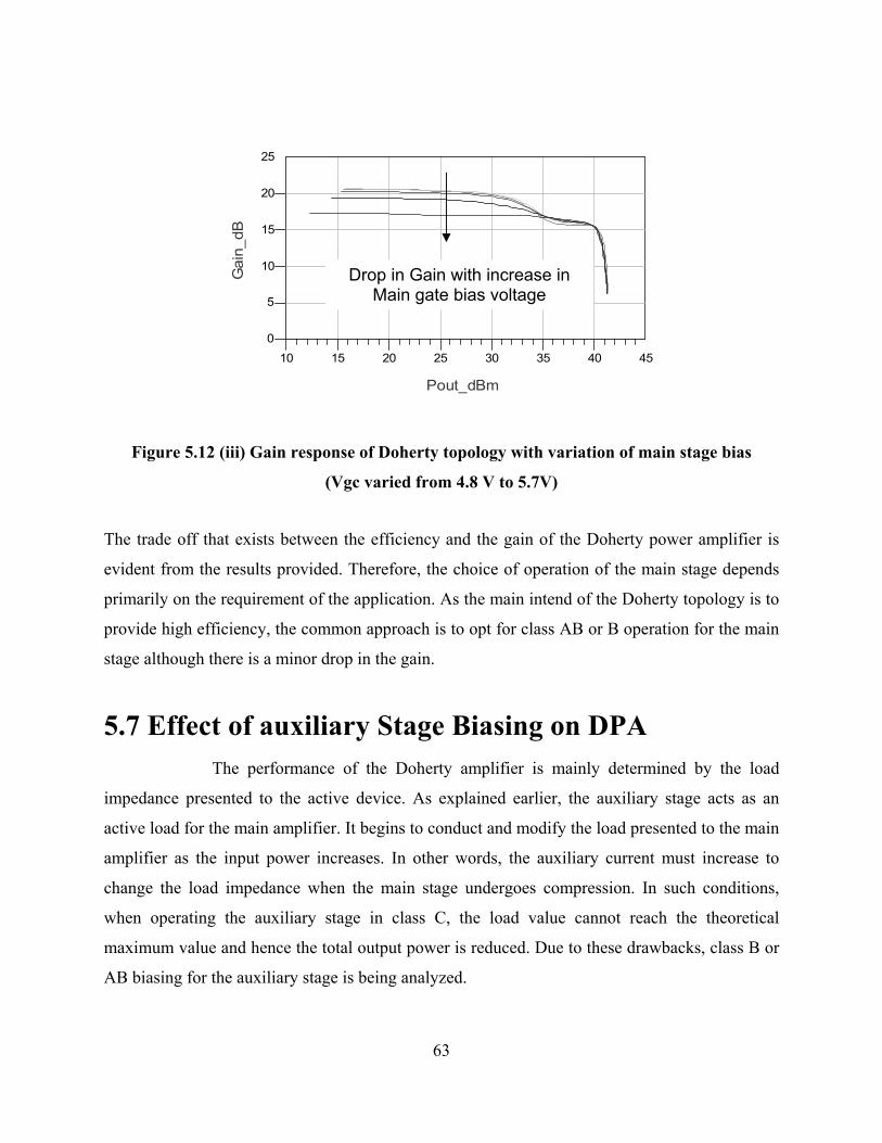
15 20 25 30 35 4010 45
5
10
15
20
0
25
Pout_dBm
Gai
n_dB
Drop in Gain with increase in Main gate bias voltage
Figure 5.12 (iii) Gain response of Doherty topology with variation of main stage bias
(Vgc varied from 4.8 V to 5.7V)
The trade off that exists between the efficiency and the gain of the Doherty power amplifier is
evident from the results provided. Therefore, the choice of operation of the main stage depends
primarily on the requirement of the application. As the main intend of the Doherty topology is to
provide high efficiency, the common approach is to opt for class AB or B operation for the main
stage although there is a minor drop in the gain.
5.7 Effect of auxiliary Stage Biasing on DPA The performance of the Doherty amplifier is mainly determined by the load
impedance presented to the active device. As explained earlier, the auxiliary stage acts as an
active load for the main amplifier. It begins to conduct and modify the load presented to the main
amplifier as the input power increases. In other words, the auxiliary current must increase to
change the load impedance when the main stage undergoes compression. In such conditions,
when operating the auxiliary stage in class C, the load value cannot reach the theoretical
maximum value and hence the total output power is reduced. Due to these drawbacks, class B or
AB biasing for the auxiliary stage is being analyzed.
63
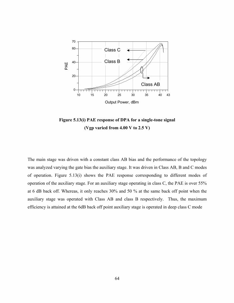
15 20 25 30 35 4010 43
20
40
60
0
70
Output Power, dBm
PAE
Class C
Class B
Class AB
Figure 5.13(i) PAE response of DPA for a single-tone signal
(Vgp varied from 4.00 V to 2.5 V)
The main stage was driven with a constant class AB bias and the performance of the topology
was analyzed varying the gate bias the auxiliary stage. It was driven in Class AB, B and C modes
of operation. Figure 5.13(i) shows the PAE response corresponding to different modes of
operation of the auxiliary stage. For an auxiliary stage operating in class C, the PAE is over 55%
at 6 dB back off. Whereas, it only reaches 30% and 50 % at the same back off point when the
auxiliary stage was operated with Class AB and class B respectively. Thus, the maximum
efficiency is attained at the 6dB back off point auxiliary stage is operated in deep class C mode
64
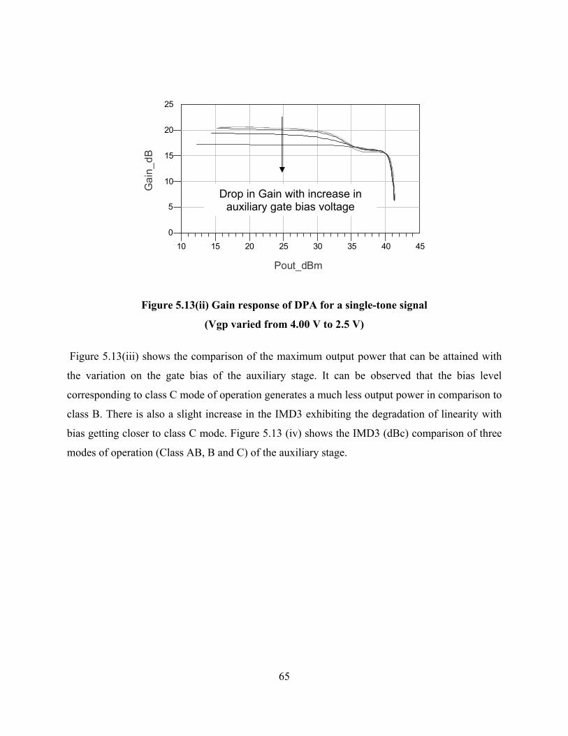
15 20 25 30 35 4010 45
5
10
15
20
0
25
Pout_dBm
Gai
n_dB
Drop in Gain with increase in auxiliary gate bias voltage
Figure 5.13(ii) Gain response of DPA for a single-tone signal
(Vgp varied from 4.00 V to 2.5 V)
Figure 5.13(iii) shows the comparison of the maximum output power that can be attained with
the variation on the gate bias of the auxiliary stage. It can be observed that the bias level
corresponding to class C mode of operation generates a much less output power in comparison to
class B. There is also a slight increase in the IMD3 exhibiting the degradation of linearity with
bias getting closer to class C mode. Figure 5.13 (iv) shows the IMD3 (dBc) comparison of three
modes of operation (Class AB, B and C) of the auxiliary stage.
65
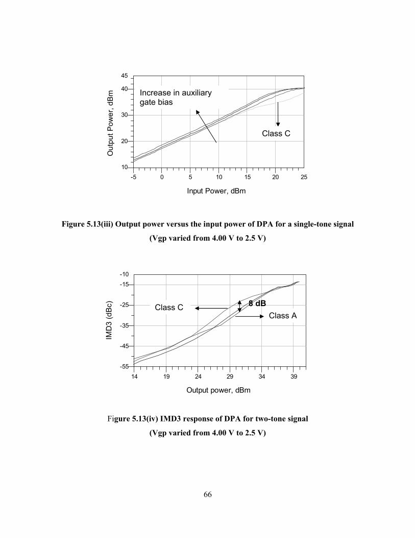
0 5 10 15 20-5 25
20
30
40
10
45
Input Power, dBm
Out
put P
ower
, dB
m Increase in auxiliary gate bias
Class C
Figure 5.13(iii) Output power versus the input power of DPA for a single-tone signal
(Vgp varied from 4.00 V to 2.5 V)
19 24 29 3414 39
-45
-35
-25
-15
-55
-10
Output power, dBm
IMD
3 (d
Bc) 8 dBClass C
Class A
Figure 5.13(iv) IMD3 response of DPA for two-tone signal
(Vgp varied from 4.00 V to 2.5 V)
66
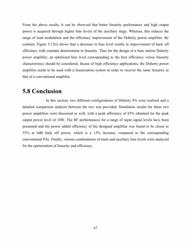
67
From the above results, it can be observed that better linearity performance and high output
power is acquired through higher bias levels of the auxiliary stage. Whereas, this reduces the
range of load modulation and the efficiency improvement of the Doherty power amplifier. By
contrast, Figure 5.13(i) shows that a decrease in bias level results in improvement of back off
efficiency with constant deterioration in linearity. Thus for the design of a base station Doherty
power amplifier, an optimized bias level corresponding to the best efficiency versus linearity
characteristics should be considered. Incase of high efficiency applications, the Doherty power
amplifier needs to be used with a linearization system in order to recover the same linearity as
that of a conventional amplifier.
5.8 Conclusion In this section, two different configurations of Doherty PA were realized and a
detailed comparison analysis between the two was provided. Simulation results for these two
power amplifiers were discussed as well, with a peak efficiency of 65% obtained for the peak
output power level of 10W. The RF performances for a range of input signal levels have been
presented and the power added efficiency of the designed amplifier was found to be closer to
55% at 6dB back off power, which is a 15% increase, compared to the corresponding
conventional PAs. Finally, various combinations of main and auxiliary bias levels were analyzed
for the optimization of linearity and efficiency.
68
Chapter 6
Summary and Conclusion
6.1 Summary This research has investigated the design and implementation of a two-stage
Doherty Power amplifier using LDMOS transistors for a base station transceiver system built to
meet the WCDMA standard. It was intended to realize a Doherty topology, with possibly
improving its characteristics as compared to the existing conventional power amplifiers and other
efficiency enhancement techniques.
In the course of this dissertation, the most common conventional PAs such as
the class AB, B and C were reviewed, as well as the currently available methods that could be
used to enhance the efficiency of a power amplifier. A detailed discussion on the theory of the
Doherty topology was provided with citations to the amplifiers built using the Vaccum tubes.
Based on the concept, an attempt was made to design two different topologies of 2.14 GHz
Doherty power amplifier for the UMTS band using LDMOS transistors that agreed with the
theory. The designs were simulated and the results were compared with that of the theoretical
Doherty amplifier as well as the corresponding conventional PAs. The influence of the main and
auxiliary stage biasing on the overall performance was also analyzed and the bias voltages were
adjusted for better cancellation of the harmonics generated by the main and auxiliary amplifiers.
69
Finally, adjusting the gate bias of the main and the auxiliary stage did optimization of linearity
with minimum reduction in the improved efficiency.
6.2 Conclusion The research has proven the feasibility of the proposed two-stage Doherty
power amplifier design in maintaining an high efficiency at the 6 dB back off power, while
maintaining a reasonable linearity performance in comparison with the conventional PA design.
The key contributions of this work can be stated as follows
• A detailed design and implementation of two different realizations of a 2.14 GHz two
stage Doherty power amplifier for the WCDMA standard. It exhibits a PAE of 55% in the
6dB back off from the 1dB compression point of 40.2 dBm.
• Bias optimization of the main and auxiliary stages for the best linearity versus efficiency
characteristics.
6.3 Future Directions This project cannot be considered exhaustively explored and the following
directions may be noted for its expansion
• Implementation of a linearization method like feed-forward or digital predistortion on
the proposed Doherty topology, as it was seen to be exhibiting a deteriorated linearity
performance in comparison to the other PA topologies.
• Further improvement in linearity could be achieved by derivative superposition principle
that would involve a design of an N-way Doherty topology [Yang01]. This would attempt
in canceling the coefficients of intermodulation distortions caused by the main amplifier
by the multiple auxiliary stages.
70
References [Camp00] C.P. Campbell, “A Fully Integrated Ku-band Doherty Amplifier MMIC,” IEEE
Microwave and Guided Wave Letters, Vol. 9, No. 3, 1999.
[Cass00] Cedric Cassan, “Efficiency enhancement techniques for power amplifier ”, Motorola confidential propriety
[Dohe00] W.H.Doherty, “A new high efficiency power amplifier for modulated waves,” Proc. IRE, Vol. 24, No. 9, September 1936, pp-1163-1182
[Grig00] Thesis Dissertation by Grigori Doudorov, “Evaluation of Si-LDMOS transistor for RF power amplifier in 2-6 GHz frequency range”, 2003.
[Iwam00] M. Iwamoto, A. Williams, Pin-Fin Chen, A. G. Metzger, L. E. Larson, Peter M. Asbeck “An Extended Doherty Amplifier With High Efficiency Over a Wide Power Range,” IEEE Trans. Microwave Theory Tech., vol. 49, No. 12, Dec. 2001.
[Koba00] K.W. Kobayashi, A.K. Oki, A. Gutierrez-Aitken, P.Chin, Li Yang, E. Kaneshiro, P.C. Grossman, K. Sato, T.R. Block, H.C. Yen, and D.C. Streit, “An 18-21 GHz InP DHBT Linear Microwave Doherty Amplifier”, IEEE RFIC Symposium, 2000.
[Mcca00] C.P. McCarroll, G.D. Alley, S.Yates, R. Matreci, “A 20GHz Doherty Power Amplifier MMIC with High Efficiency and Low Distortion Designed for Broad Digital Communication Systems,” IEEE MTT-S Digest, 2000.
[Mamc00] R. J. McMarrow, D.M. Upton et P. R. Maloney, “ The Microwave Doherty amplifier,” IEEE MTT-S Digest, 1994, pp. 1652-1656
[Pete00] Peter B. Kenington, “ High-Linearity RF Amplifier Design,” Artech House, Edition 2000.
[Phil00] Product news from Philips semiconductors, ”LDMOS devices to boost base station efficiency,” 7 Nov 2003
[Poth00] N.Pothecary, “Feed-forward Linear Power Amplifier,” Artech House, Edition 1999
71
[Raab00] F.H. Raab, “Efficiency of Doherty RF power-amplifier systems,” IEEE Trans. On Broadcasting, Vol. BC-33, No. 3, September 1987, pp. 77-83
[Raab01]
F.H. Raab, P.M. Asbeck, S. Cripps, P.B. Kenington, Z. B. Popovic, N. Pothecary, J. F.Sevic, and N. O. Sokal, “Power amplifiers and transmitters for RF and microwave, ” IEEE Trans. Microwave Theory Tech., vol. 50, pp. 814-826, Mar. 2002.
[Stev00] Steve C. Cripps, “RF Power Amplifiers for Wireless Communications,” Artech House, Edition 1999
[Stev01] Steve C. Cripps, “Advanced Techniques in RF Power Amplifier Design,” Edition 1999
[West00] Western Electric Transmitters publication, “A development of Bell Telephone Laboratories - The Doherty Amplifier”
[Yang00] Y. Yang, J. Yi, Y.Y. Woo and B. Kim, “Experimental Investigation on Efficiency and Linearity of a Microwave Doherty Amplifier, “IEEE MTT-S International Microwave Symposium Digest, May 2001, pp. 1367-1370.
[Yang01] Y. Yang, J. Cha, B. Shin, B. Kim, “A Fully N-Way Doherty Amplifier With Optimized Linearity, ” IEEE Trans. Microwave Theory Tech., vol. 51, No. 3, Mar. 2003.
[Yang02] Y. Yang, J. Cha, B. Shin, B. Kim, “ Optimum Design for Linearity and Efficiency of a Microwave Doherty Amplifier Using a New Load Matching Technique,” Microwave Journal, September 2003.
72
Vita
Vani Viswanathan received her M.S.E.E. in 2004 from Virginia Tech and
B.E in Electronics and Instrumentation Engineering from the University of Madras in Chennai,
India, in 2001. During the course of her graduate studies, she was a research assistant at Virginia
Tech’s Center for Wireless Telecommunications. She joined Panasonic Mobile Communications
Development Corporation in February 2004, where she now serves as a RF Design Engineer
involved in the design and testing of the RF transmitter and receiver sections of wireless
handsets. Her research interest includes wireless communications and high efficiency power
amplifier designs.


![Market Challenges v2 Internal Keynote [Read-Only]data.eefocus.com/openhard/source/44f49bed4e120e1a6c3ec9885aedc… · Edge of the network ... Seminar in a box eLearning Design Acceleration](https://img.pdfslide.us/doc/110x75/5ad2a08d7f8b9afa798ce9af/market-challenges-v2-internal-keynote-read-onlydata-edge-of-the-network-.jpg)


![Layout 1.ps [ 1 ] , page 1-78 @ Normalize ( Haisan Annual ...libapps2.nus.edu.sg/nus_hl/haisan32005.pdfefficiency and productivity of inventory management and maximise capacity utilisation](https://img.pdfslide.us/doc/110x75/5b17f1077f8b9a23258b5564/layout-1ps-1-page-1-78-normalize-haisan-annual-and-productivity-of.jpg)