Embed Size (px)
Citation preview
PAL / POSTECH
Efficiency analysis of a capacitor charging power supply for a pulsed klystron-modulator*
Efficiency analysis of a capacitor charging power supply for a pulsed klystron-modulator*
J. S. Oh, S. D. Jang, Y. G. Son, M. H. Cho, W. Namkung, PAL/POSTECH, Pohang, Korea
S. C. RoDong-A Hitech Co. Ltd., Busan, Korea
Korean Physical Society Hanyang University, Korea
October 24 – 26, 2002
* Work supported in part by Pohang Iron and Steel Company (POSCO) and MOST.
PAL / POSTECH
AbstractAbstract
A current source, inverter power supply is best choice for a capacitor-charging power supply of a pulsed klystron-modulator. Its high frequency technology makes the system size small and the regulation fine. The command-charging feature of the inverter guarantees higher reliability of switching function.
Thermal design is most critical in this power supply so the analysis of the system efficiency is essential. Better efficiency can be obtained through accurate evaluation of power loss distribution.
Design and fabrication detail of an air-cooled 50-kV, 15-kW inverter charging supply are presented. The efficiency and the stability of the power supply are estimated and examined.
PAL / POSTECH
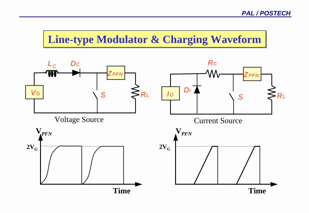
Line-type Modulator & Charging WaveformLine-type Modulator & Charging Waveform
LC
RL
DC
IG
RC
Z ZPFN PFN
VGDI
S RLS
Voltage Source Current SourceVVPFN
2VG
PFN
2VG
Time Time
PAL / POSTECH
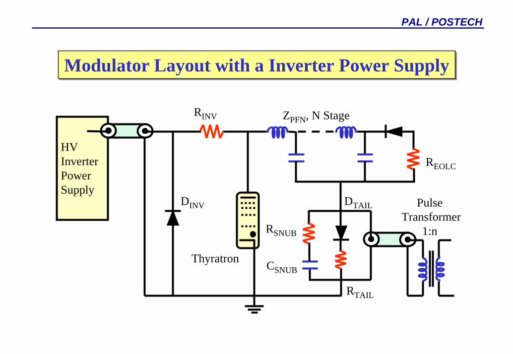
Modulator Layout with a Inverter Power Supply Modulator Layout with a Inverter Power Supply
Thyratron
HVInverterPowerSupply
ZPFN, N Stage
Pulse Transformer
1:n
DINV DTAIL
RTAIL
RSNUB
CSNUB
REOLC
RINV
PAL / POSTECH
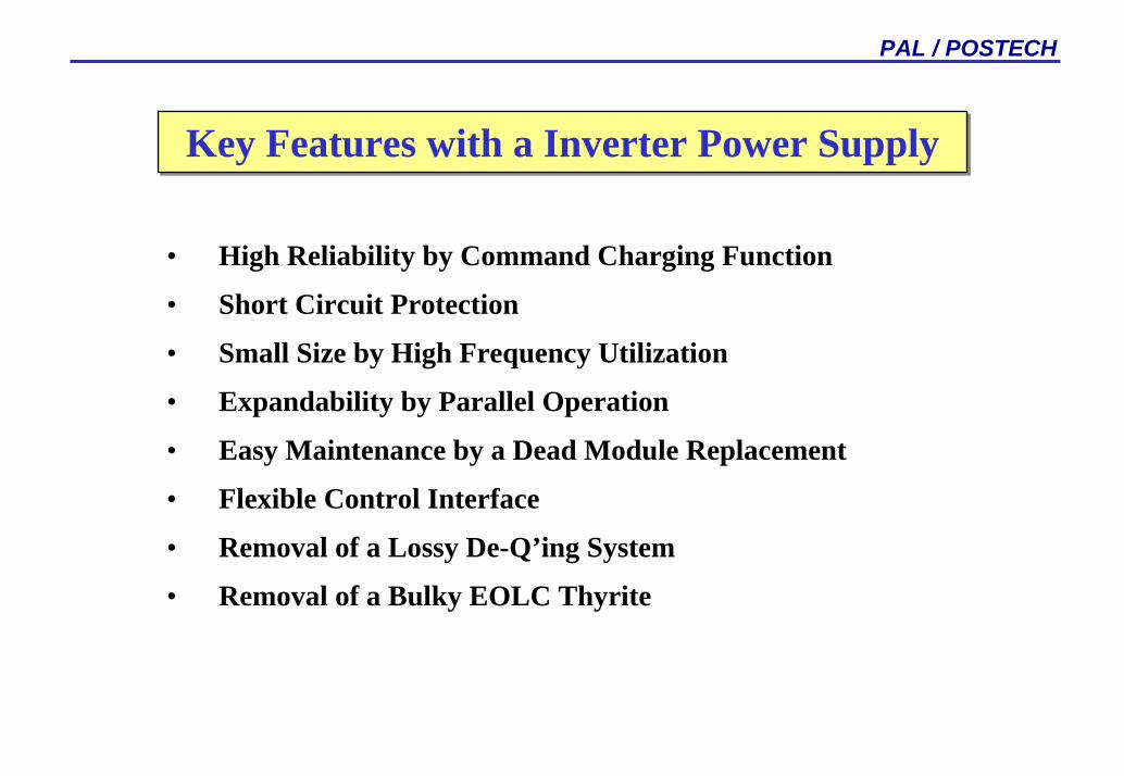
Key Features with a Inverter Power Supply Key Features with a Inverter Power Supply
• High Reliability by Command Charging Function
• Short Circuit Protection
• Small Size by High Frequency Utilization
• Expandability by Parallel Operation
• Easy Maintenance by a Dead Module Replacement
• Flexible Control Interface
• Removal of a Lossy De-Q’ing System
• Removal of a Bulky EOLC Thyrite
PAL / POSTECH
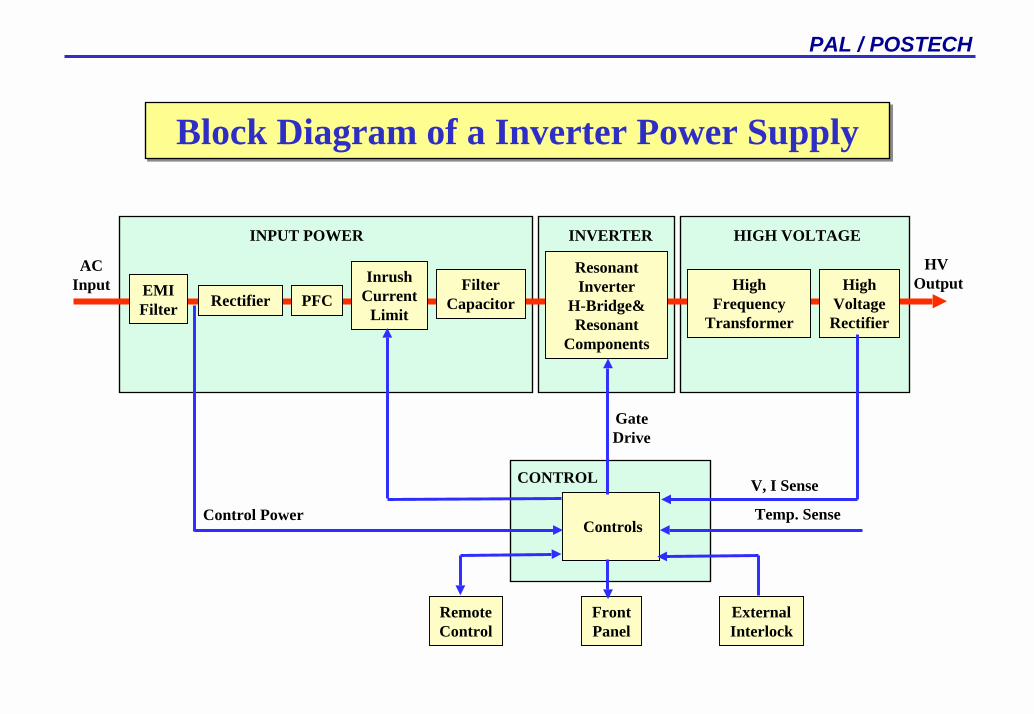
Block Diagram of a Inverter Power SupplyBlock Diagram of a Inverter Power Supply
EMIFilter Rectifier PFC
InrushCurrent
Limit
FilterCapacitor
ResonantInverter
H-Bridge&Resonant
Components
HighFrequency
Transformer
HighVoltageRectifier
Controls
FrontPanel
RemoteControl
ExternalInterlock
Control Power
V, I Sense
Temp. Sense
GateDrive
INPUT POWER INVERTER HIGH VOLTAGE
HV Output
ACInput
CONTROL
PAL / POSTECH
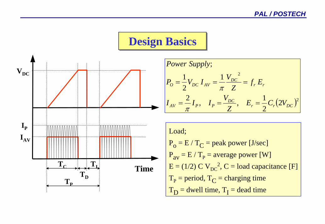
Design BasicsDesign Basics
( )2
2
221,,2
121
;
DCrrDC
PPAV
rrDC
AVDCO
VCEZ
VIII
EfZ
VIVP
SupplyPower
===
===
π
π
TC
TP
TD
TI
VDC
IP Load;Po = E / TC = peak power [J/sec]Pav = E / TP = average power [W] E = (1/2) C VDC
2, C = load capacitance [F]TP = period, TC = charging timeTD = dwell time, TI = dead time
IAV
Time
PAL / POSTECH
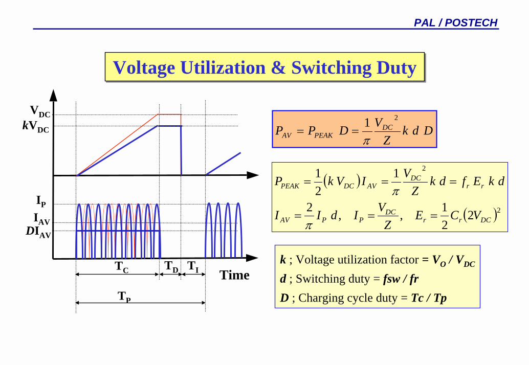
Voltage Utilization & Switching DutyVoltage Utilization & Switching Duty
( )
( )2
2
221,,2
121
DCrrDC
PPAV
rrDC
AVDCPEAK
VCEZ
VIdII
dkEfdkZ
VIVkP
===
===
π
π
VDC
IAV
IP
TC TD
kVDC
DIAV
DdkZ
VDPP DCPEAKAV
21π
==
k ; Voltage utilization factor = VO / VDC
d ; Switching duty = fsw / frD ; Charging cycle duty = Tc / Tp
TI TimeTP
PAL / POSTECH
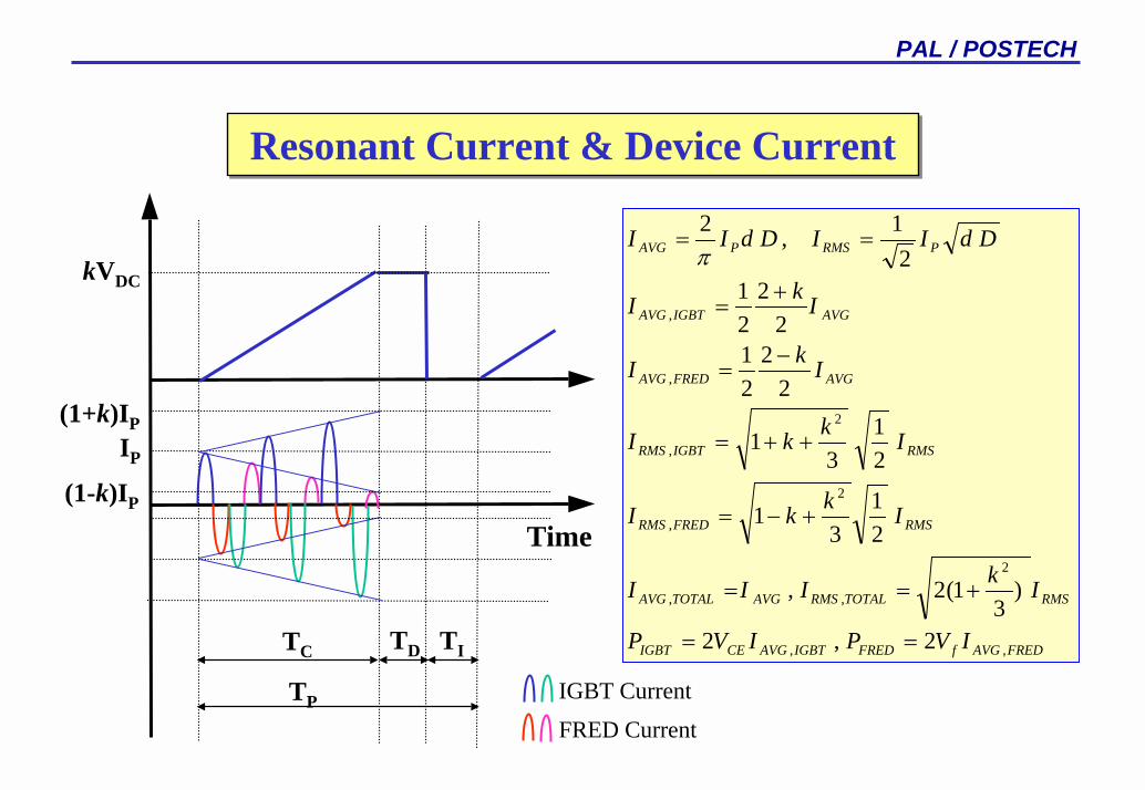
Resonant Current & Device CurrentResonant Current & Device Current
FREDAVGfFREDIGBTAVGCEIGBT
RMSTOTALRMSAVGTOTALAVG
RMSFREDRMS
RMSIGBTRMS
AVGFREDAVG
AVGIGBTAVG
PRMSPAVG
IVPIVP
IkIII
IkkI
IkkI
IkI
IkI
DdIIDdII
,,
2
,,
2
,
2
,
,
,
2,2
)3
1(2,
21
31
21
31
22
21
22
21
21,2
==
+==
+−=
++=
−=
+=
==π
Time
IP
TP
TD
(1+k)IP
kVDC
(1-k)IP
TITC
IGBT Current
FRED Current
PAL / POSTECH
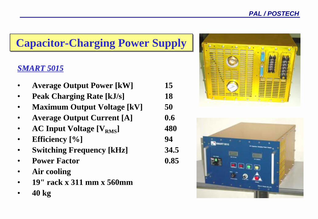
SMART 5015SMART 5015
• Average Output Power [kW] 15• Peak Charging Rate [kJ/s] 18• Maximum Output Voltage [kV] 50• Average Output Current [A] 0.6• AC Input Voltage [VRMS] 480• Efficiency [%] 94• Switching Frequency [kHz] 34.5• Power Factor 0.85• Air cooling• 19" rack x 311 mm x 560mm• 40 kg
Capacitor-Charging Power SupplyCapacitor-Charging Power Supply
PAL / POSTECH
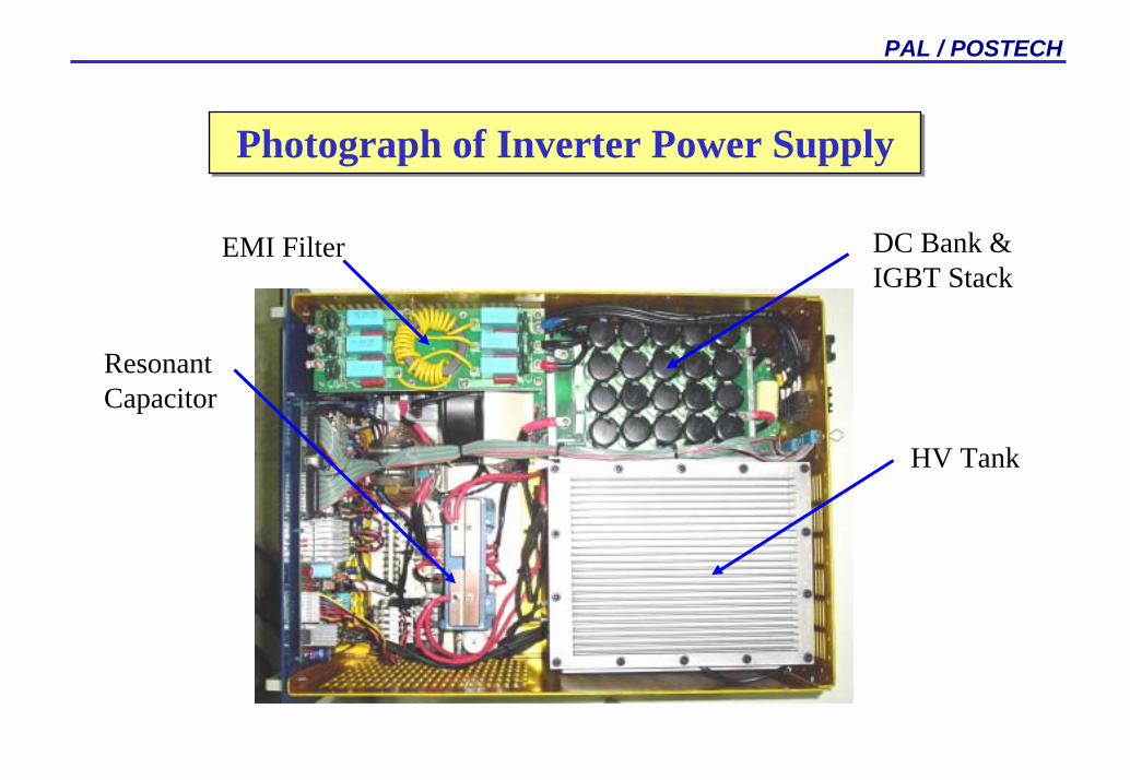
Photograph of Inverter Power SupplyPhotograph of Inverter Power Supply
EMI Filter
ResonantCapacitor
DC Bank &IGBT Stack
HV Tank
PAL / POSTECH
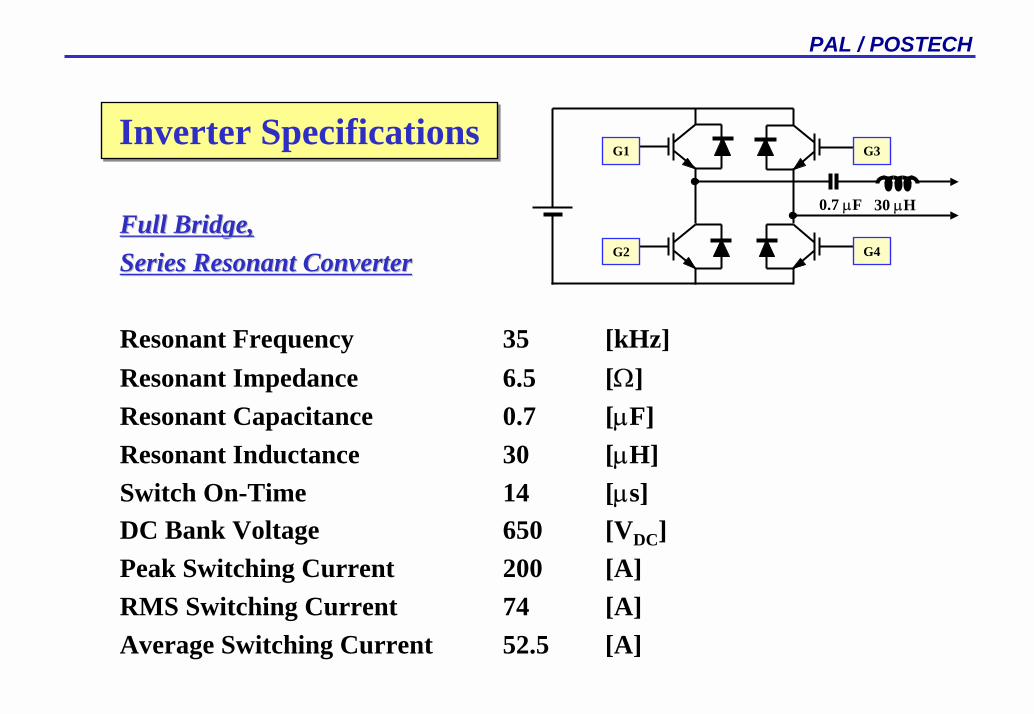
Full Bridge, Full Bridge, Series Resonant ConverterSeries Resonant Converter
Resonant Frequency 35 [kHz]Resonant Impedance 6.5 [Ω] Resonant Capacitance 0.7 [µF] Resonant Inductance 30 [µH] Switch On-Time 14 [µs] DC Bank Voltage 650 [VDC]Peak Switching Current 200 [A] RMS Switching Current 74 [A] Average Switching Current 52.5 [A]
Inverter SpecificationsInverter SpecificationsG1
G2
G3
G4
30 µH0.7 µF
PAL / POSTECH
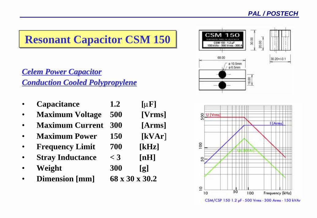
Resonant Capacitor CSM 150Resonant Capacitor CSM 150
Celem Power CapacitorCelem Power CapacitorConduction Cooled PolypropyleneConduction Cooled Polypropylene
• Capacitance 1.2 [µF]• Maximum Voltage 500 [Vrms]• Maximum Current 300 [Arms]• Maximum Power 150 [kVAr]• Frequency Limit 700 [kHz]• Stray Inductance < 3 [nH]• Weight 300 [g]• Dimension [mm] 68 x 30 x 30.2
PAL / POSTECH
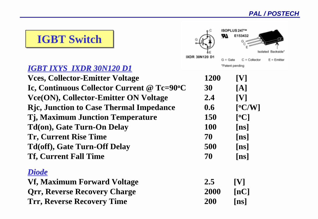
IGBT IXYS IXDR 30N120 D1IGBT IXYS IXDR 30N120 D1Vces, Collector-Emitter Voltage 1200 [V]Ic, Continuous Collector Current @ Tc=90oC 30 [A] Vce(ON), Collector-Emitter ON Voltage 2.4 [V]Rjc, Junction to Case Thermal Impedance 0.6 [oC/W]Tj, Maximum Junction Temperature 150 [oC]Td(on), Gate Turn-On Delay 100 [ns]Tr, Current Rise Time 70 [ns]Td(off), Gate Turn-Off Delay 500 [ns]Tf, Current Fall Time 70 [ns]
DiodeDiodeVf, Maximum Forward Voltage 2.5 [V]Qrr, Reverse Recovery Charge 2000 [nC]Trr, Reverse Recovery Time 200 [ns]
IGBT SwitchIGBT Switch
PAL / POSTECH
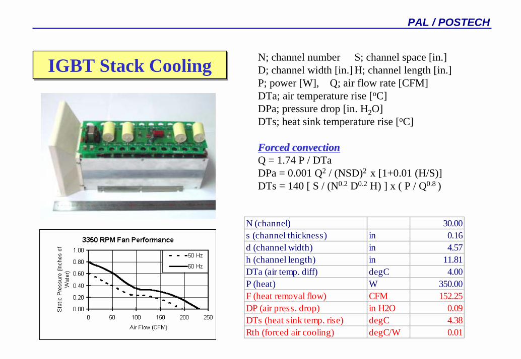
IGBT Stack CoolingIGBT Stack Cooling N; channel number S; channel space [in.]D; channel width [in.] H; channel length [in.]P; power [W], Q; air flow rate [CFM]DTa; air temperature rise [oC]DPa; pressure drop [in. H2O]DTs; heat sink temperature rise [oC]
Forced convectionForced convectionQ = 1.74 P / DTaDPa = 0.001 Q2 / (NSD)2 x [1+0.01 (H/S)]DTs = 140 [ S / (N0.2 D0.2 H) ] x ( P / Q0.8 )
N (channel) 30.00s (channel thickness) in 0.16d (channel width) in 4.57h (channel length) in 11.81DTa (air temp. diff) degC 4.00P (heat) W 350.00F (heat removal flow) CFM 152.25DP (air press. drop) in H2O 0.09DTs (heat sink temp. rise) degC 4.38Rth (forced air cooling) degC/W 0.01
PAL / POSTECH
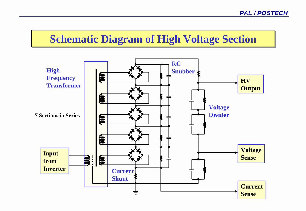
Schematic Diagram of High Voltage SectionSchematic Diagram of High Voltage Section
HVOutput
CurrentSense
VoltageSenseInput
fromInverter
HighFrequencyTransformer
VoltageDivider
CurrentShunt
RCSnubber
7 Sections in Series
PAL / POSTECH
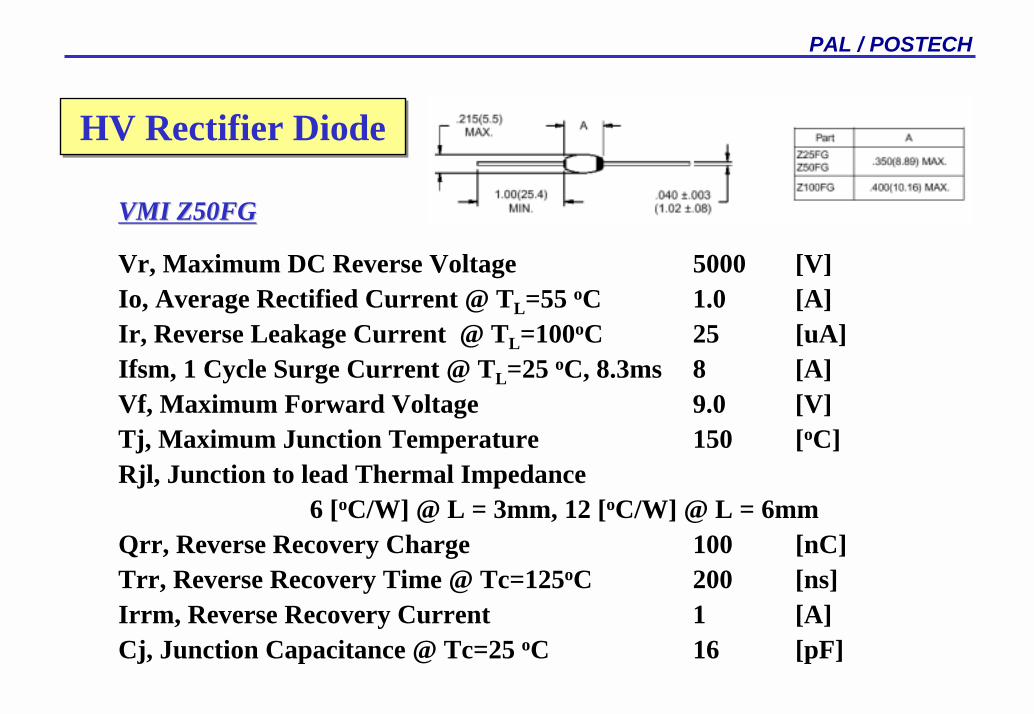
VMI Z50FGVMI Z50FG
Vr, Maximum DC Reverse Voltage 5000 [V]Io, Average Rectified Current @ TL=55 oC 1.0 [A]Ir, Reverse Leakage Current @ TL=100oC 25 [uA] Ifsm, 1 Cycle Surge Current @ TL=25 oC, 8.3ms 8 [A]Vf, Maximum Forward Voltage 9.0 [V]Tj, Maximum Junction Temperature 150 [oC]Rjl, Junction to lead Thermal Impedance
6 [oC/W] @ L = 3mm, 12 [oC/W] @ L = 6mm Qrr, Reverse Recovery Charge 100 [nC]Trr, Reverse Recovery Time @ Tc=125oC 200 [ns]Irrm, Reverse Recovery Current 1 [A]Cj, Junction Capacitance @ Tc=25 oC 16 [pF]
HV Rectifier DiodeHV Rectifier Diode
PAL / POSTECH
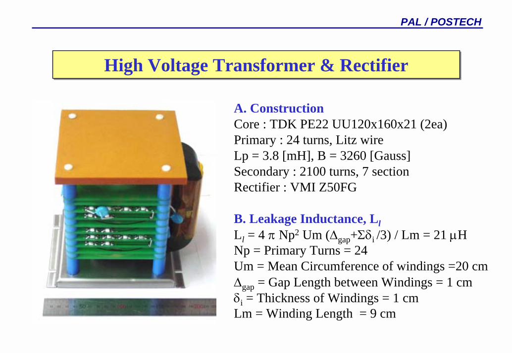
High Voltage Transformer & RectifierHigh Voltage Transformer & Rectifier
A. ConstructionCore : TDK PE22 UU120x160x21 (2ea)Primary : 24 turns, Litz wireLp = 3.8 [mH], B = 3260 [Gauss]Secondary : 2100 turns, 7 sectionRectifier : VMI Z50FG
B. Leakage Inductance, LlLl = 4 π Np2 Um (∆gap+Σδi /3) / Lm = 21 µH Np = Primary Turns = 24Um = Mean Circumference of windings =20 cm∆gap = Gap Length between Windings = 1 cmδi = Thickness of Windings = 1 cmLm = Winding Length = 9 cm
PAL / POSTECH
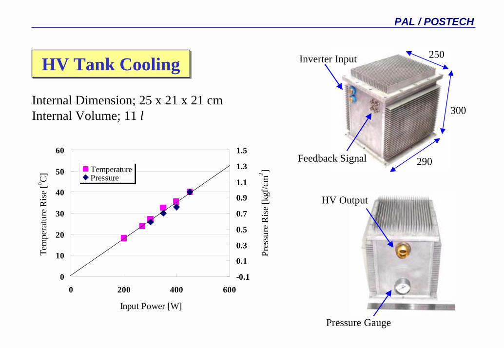
HV Tank CoolingHV Tank Cooling Inverter Input
Feedback Signal 290
300
250
Internal Dimension; 25 x 21 x 21 cmInternal Volume; 11 l
0
10
20
30
40
50
60
0 200 400 600
Input Power [W]
Tem
pera
ture
Ris
e [o C
]
-0.1
0.1
0.3
0.5
0.7
0.9
1.1
1.3
1.5
Pres
sure
Ris
e [k
gf/c
m2 ]Temperature
Pressure
HV Output
Pressure Gauge
PAL / POSTECH
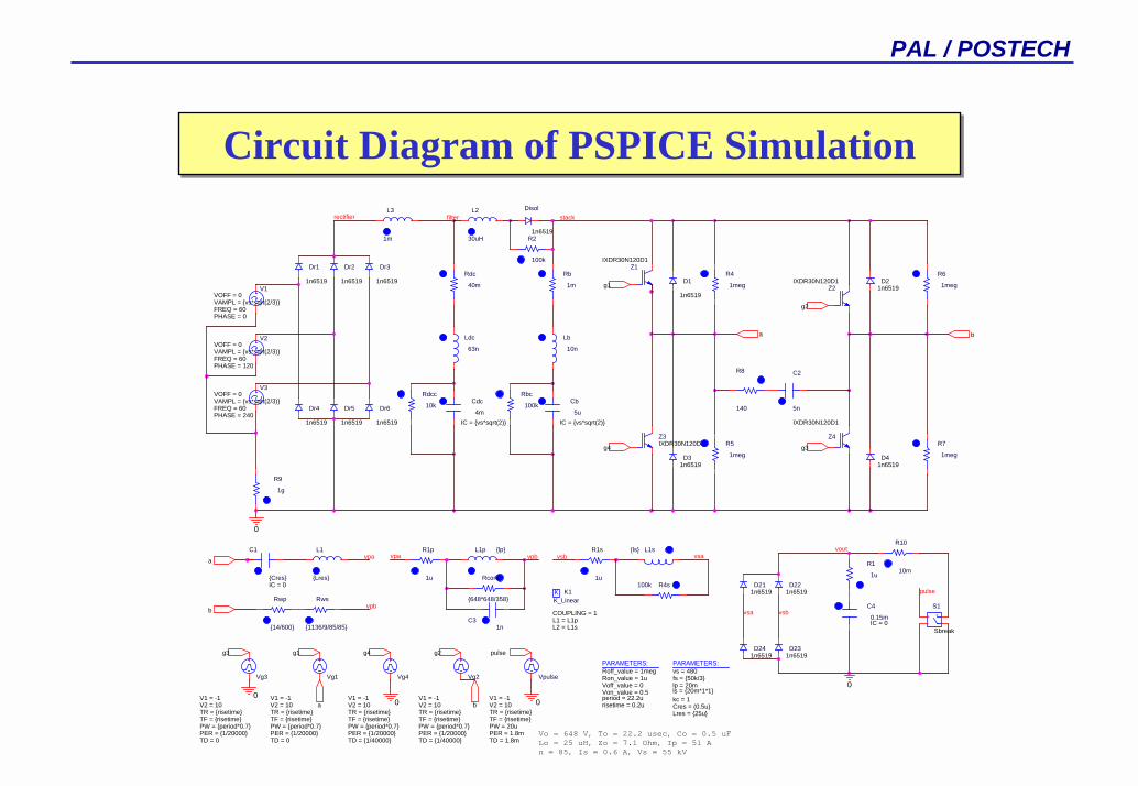
Circuit Diagram of PSPICE SimulationCircuit Diagram of PSPICE Simulation
V3
FREQ = 60VAMPL = vs*sqrt(2/3)VOFF = 0
PHASE = 240
Vpulse
TD = 1.8m
TF = risetimePW = 20uPER = 1.8m
V1 = -1
TR = risetimeV2 = 10
C2
5n
R6
1meg1n6519
Dr1
Vg3
TD = 0
TF = risetimePW = period*0.7PER = 1/20000
V1 = -1
TR = risetimeV2 = 10
L1
Lres
vsb
R2
100k
Vg4
TD = 1/40000
TF = risetimePW = period*0.7PER = 1/20000
V1 = -1
TR = risetimeV2 = 10
Cdc
4mIC = vs*sqrt(2)
1n6519D21
pulse
1n6519
Dr3
R1s
1u
vpbvsa
vpb
g2
1n6519
Dr2
g1
Cb
5uIC = vs*sqrt(2)
1n6519D23
Rdcc
10k
1n6519D22
L2
30uH
R10
10m
Ldc
63n
R7
1meg
Z1IXDR30N120D1
Vg1
TD = 0
TF = risetimePW = period*0.7PER = 1/20000
V1 = -1
TR = risetimeV2 = 10
V1
FREQ = 60VAMPL = vs*sqrt(2/3)VOFF = 0
PHASE = 0
0
filter
1n6519
D1
Z3IXDR30N120D1
b
0
R8
140
R5
1megg3
Z4
IXDR30N120D1
vpa
C31n
stack
R1p
1u
a
1n6519
Dr4
Rbc
100k
pulse
L1p lp
C4
0.15mIC = 0
1n6519D24
a
1n6519
Disol
0
vsa
Z2IXDR30N120D1
V2
FREQ = 60VAMPL = vs*sqrt(2/3)VOFF = 0
PHASE = 120
Vg2
TD = 1/40000
TF = risetimePW = period*0.7PER = 1/20000
V1 = -1
TR = risetimeV2 = 10
rectifier
g3
1n6519D4
1n6519D2
1n6519
Dr5
g4
Rcore
648*648/358Rwp
14/600
Lb
10n
Vo = 648 V, To = 22.2 usec, Co = 0.5 uFLo = 25 uH, Zo = 7.1 Ohm, Ip = 51 An = 85, Is = 0.6 A, Vs = 55 kV
L1sls
+-
+
-Sbreak
S1
R1
1u
g1
vsb
a
b
R4
1meg
vout
PARAMETERS:vs = 480fs = 50k/3lp = 20mls = 20m*1*1kc = 1Cres = (0.5uLres = 25u
1n6519D3
Rdc
40m
Rws
1136/9/85/85
C1
CresIC = 0
0
0
PARAMETERS:Roff_value = 1megRon_value = 1uVoff_value = 0Von_value = 0.5period = 22.2urisetime = 0.2u
Rb
1m
K K1
COUPLING = 1
K_Linear
L1 = L1pL2 = L1s
1n6519
Dr6
L3
1m
g2
vpa
R9
1g
g4
R4s100k
b
PAL / POSTECH
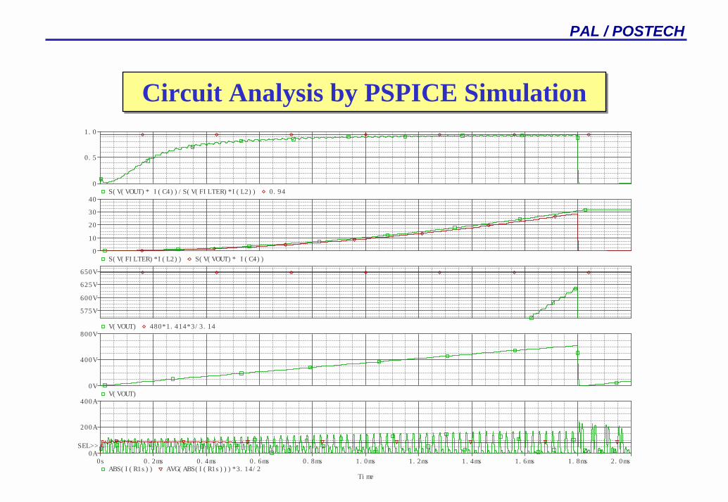
Circuit Analysis by PSPICE SimulationCircuit Analysis by PSPICE Simulation
Ti me
0s 0. 2ms 0. 4ms 0. 6ms 0. 8ms 1. 0ms 1. 2ms 1. 4ms 1. 6ms 1. 8ms 2. 0msABS( I ( R1s ) ) AVG( ABS( I ( R1s ) ) ) *3. 14/ 2
0A
200A
400A
SEL>>
V( VOUT)0V
400V
800VV( VOUT) 480*1. 414*3/ 3. 14
575V
600V
625V
650V
S( V( FI LTER) *I ( L2) ) S( V( VOUT) * I ( C4) )0
10
20
30
40S( V( VOUT) * I ( C4) ) / S( V( FI LTER) *I ( L2) ) 0. 94
0
0. 5
1. 0
PAL / POSTECH
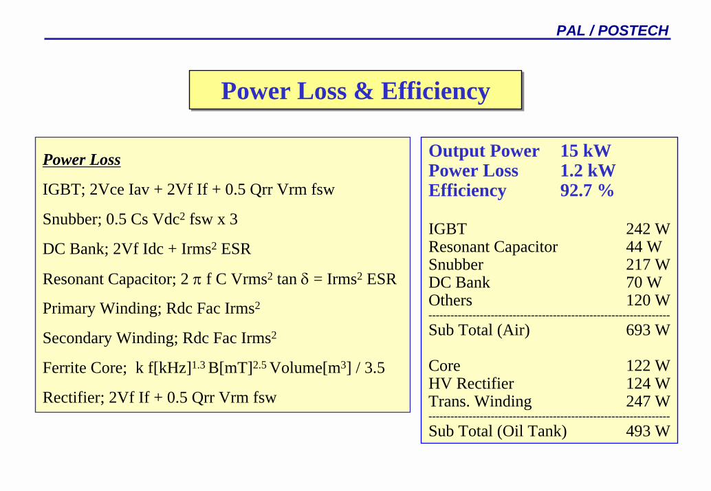
Power Loss & EfficiencyPower Loss & Efficiency
Output Power 15 kWPower Loss 1.2 kWEfficiency 92.7 %
IGBT 242 WResonant Capacitor 44 WSnubber 217 WDC Bank 70 WOthers 120 W------------------------------------------------------------------Sub Total (Air) 693 W
Core 122 WHV Rectifier 124 WTrans. Winding 247 W------------------------------------------------------------------Sub Total (Oil Tank) 493 W
Power LossPower Loss
IGBT; 2Vce Iav + 2Vf If + 0.5 Qrr Vrm fsw
Snubber; 0.5 Cs Vdc2 fsw x 3
DC Bank; 2Vf Idc + Irms2 ESR
Resonant Capacitor; 2 π f C Vrms2 tan δ = Irms2 ESR
Primary Winding; Rdc Fac Irms2
Secondary Winding; Rdc Fac Irms2
Ferrite Core; k f[kHz]1.3 B[mT]2.5 Volume[m3] / 3.5
Rectifier; 2Vf If + 0.5 Qrr Vrm fsw
PAL / POSTECH
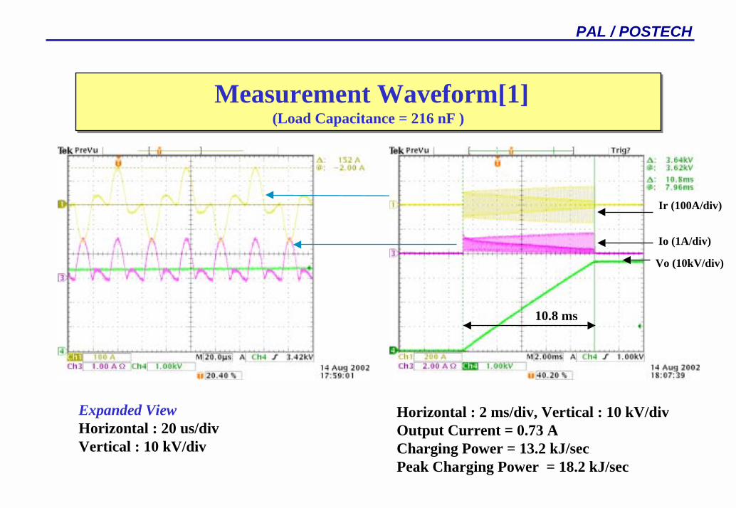
Measurement Waveform[1](Load Capacitance = 216 nF )
Measurement Waveform[1](Load Capacitance = 216 nF )
10.8 ms
Ir (100A/div)
Io (1A/div)
Vo (10kV/div)
Expanded ViewHorizontal : 20 us/divVertical : 10 kV/div
Horizontal : 2 ms/div, Vertical : 10 kV/divOutput Current = 0.73 ACharging Power = 13.2 kJ/secPeak Charging Power = 18.2 kJ/sec
PAL / POSTECH
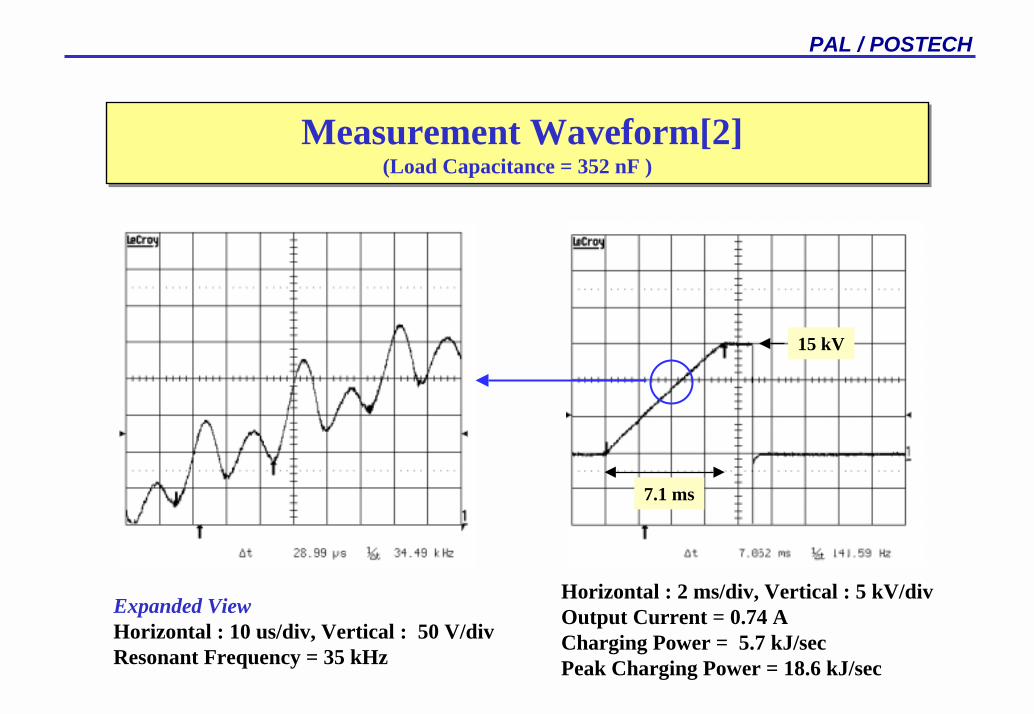
Measurement Waveform[2](Load Capacitance = 352 nF )
Measurement Waveform[2](Load Capacitance = 352 nF )
7.1 ms
15 kV
Horizontal : 2 ms/div, Vertical : 5 kV/divOutput Current = 0.74 ACharging Power = 5.7 kJ/secPeak Charging Power = 18.6 kJ/sec
Expanded ViewHorizontal : 10 us/div, Vertical : 50 V/divResonant Frequency = 35 kHz
PAL / POSTECH
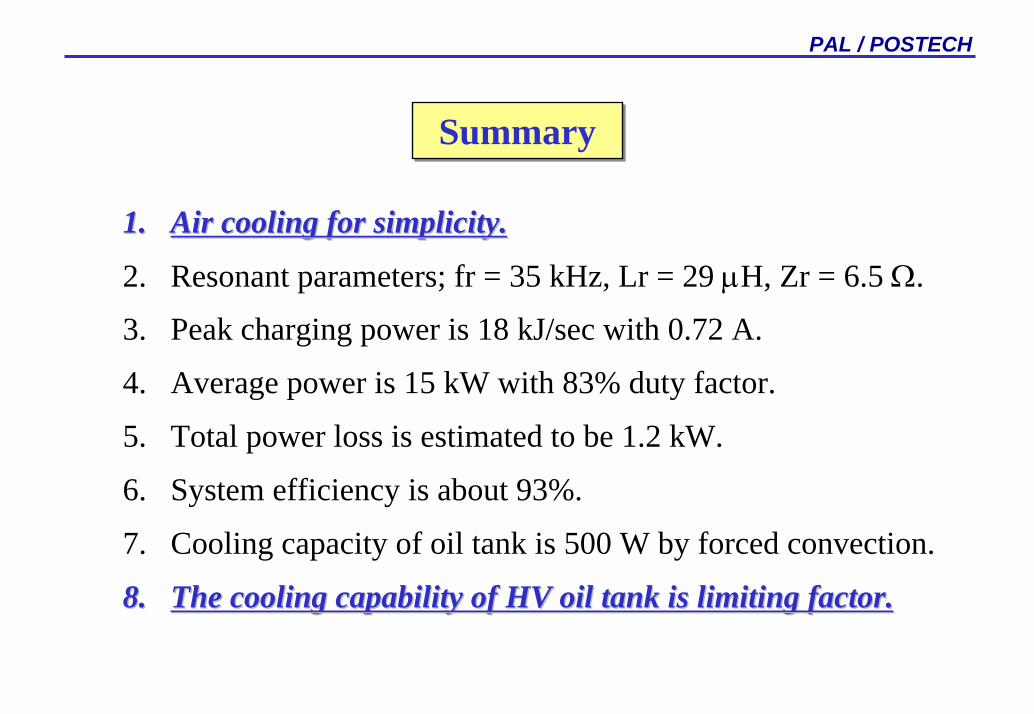
SummarySummary
1.1. Air cooling for simplicity.Air cooling for simplicity.
2. Resonant parameters; fr = 35 kHz, Lr = 29 µH, Zr = 6.5 Ω.
3. Peak charging power is 18 kJ/sec with 0.72 A.
4. Average power is 15 kW with 83% duty factor.
5. Total power loss is estimated to be 1.2 kW.
6. System efficiency is about 93%.
7. Cooling capacity of oil tank is 500 W by forced convection.
8.8. The cooling capability of HV oil tank is limiting factor.The cooling capability of HV oil tank is limiting factor.