Embed Size (px)
Citation preview

Digest Journal of Nanomaterials and Biostructures Vol. 16, No. 3, July - September 2021, p. 1127 - 1136
Effects of gold film thickness and annealing time on diameter
of silicon nanowires grown by VLS process
Z. Lia, A.-J. Tang
b,1, S.-Y. Tang
b, D.-W. Hu
a, H.-X. Tian
a, W. Wang
a
aSchool of Chemistry and Chemical Engineering, Guizhou University, Guiyang
550025, China bSchool of Chemical Engineering, Guizhou Institute of Technology, Guiyang
550003, China
In this paper, silicon nanowires were prepared by chemical vapor deposition (CVD) in the
presence of gold catalyst. We discussed the effects of gold film thickness and annealing
time on droplet diameter and silicon nanowire diameter. The study revealed that the
diameter of silicon nanowires increases with the increase of the thickness of the gold film.
With the increase of annealing time, the number of alloy droplets decreases, and the
diameter increases. The average diameter of silicon nanowires decreases first and then
increases. The results provide useful information for long-time annealing of silicon
nanowires.
(Received April 16, 2021; Accepted August 18, 2021)
Keywords: Silicon nanowires, Annealing, Alloy droplets, VLS growth mechanism
1. Introduction
In recent years, silicon nanowires (SiNWs) have been widely used in many fields such as
biosensors, field-effect transistors, photocatalytic and solar cells due to their unique properties [1-
7]. The earliest studies of SiNWs date back to the mid-20th century. When Treuting and Arnold[8]
first created silicon whiskers with <111> orientation on their crystal surfaces. In 1964, Wagner and
Ellis [9] proposed the earliest gas-liquid-solid growth mechanism of SiNWs, which was also one
of the most common growth mechanisms in the preparation of SiNWs. Then, because of the
limitations of its technology and application, the study of SiNWs began to enter a window period,
during which there was no great progress in its research. It was not until the advent of carbon
nanotubes in 1991 that many researchers began to consider silicon, a carbon homolog [10]. SiNWs
and silicon nanotubes have become a hot spot of scientific research. Initially, researchers used the
electron beam lithography combined with reactive ion etching [11-13] to produce SiNWs, but this
time-consuming, complex and expensive method has not been widely used, and scanning
tunneling microscopes were few in number and present major problems in detecting
characterization. In 1998, Lieber and Zhang [14-15] prepared a large number of SiNWs by laser
ablation method based on VLS growth mechanism. Since then, many researchers have become
increasingly interested in the uncharted territory of SiNWs. At present, there are two ways to grow
SiNWs: "top-down" and "bottom-up". "Top-down" means using large substrates (cm to micron) to
etch the nanowire structures we need using the corresponding etching technology; "Bottom-up" is
to use small structural units (atoms, molecules, etc.) to form a relatively large and complex
structural system (nanometer scale) through interaction and self-assembly, similar to building a
house from the foundation, step by step up to build a complex and beautiful overall structure.
There are many methods to prepare SiNWs, such as molecular beam epitaxy (MBE), laser ablation
(LA), oxide assisted growth (OAG), solution method, chemical vapor deposition (CVD) [16-19],
etc. Among them, the most commonly used method is the CVD, which requires lower process
conditions, simple equipment, easy to manufacture, and the product can be prepared in large
quantities. These methods usually require the involvement of the catalyst. Common catalysts
include Al, Zn, Cu, Sn, Pt, In, Fe, Au [15,19-25], etc. Au has the most stable chemical properties,
which is suitable for the preparation of SiNWs by the method described in this paper. Only a few
1Corresponding author: [email protected]

1128
nanometers to tens of nanometers, the dosage is small, the cost is low, and the product is not easy
to be polluted. In the current research reports on the preparation of SiNWs using Au catalyst, few
researchers have studied the effects of the thickness of the gold film and annealing time on the
growth of alloy droplets and SiNWs. Hannon's group [26] studied the effect of Au surface
migration on the growth of SiNWs, and the annealing time was up to 250s. Gomatsi [27] studied
the influence of gold film thickness and annealing conditions on the VLS-assisted growth of ZnO
nanostructure in 2014 and focused on the morphology of the formed nanoparticles. The
experimental results were consistent with the theoretical prediction, which is of great help and
reference for the study in this paper. So that our study to fill a small gap in the growth of silicon
nanowire research.
2. Experimental section
Materials: H2 (99.999%) and Ar (99.999%) were purchased from Shen Jian (Guiyang,
China). Silicon tetrachloride (SiCl4, 99.5%) was purchased from Aladdin (Shanghai, China) and
wafers (1×1 cm P-type < 111 > crystalline, resistivity 1-100Ω·cm) were purchased from Richter
Silicon Materials (Zhejiang, China).
SiNWs were grown in a high-temperature tube furnace by chemical vapor deposition
(CVD). First, a silicon wafer of a certain coating thickness is placed in the ceramic boat, then the
ceramic boat is placed in the middle of the quartz tube, and then the quartz tube is placed in a high-
temperature tubular furnace (the ceramic boat is in the constant temperature area of the tubular
furnace). The two ends of the quartz tube are connected to other equipment through a
Polytetrafluoroethylene (PTFE) tube. The tubular furnace was programmed to heat up to 950℃
(the heating rate is shown in the Fig. 1). During the heating process, the Ar (1000 sccm) was used
to purge (remove the oxygen in the system) and then annealed to form Au-Si alloy droplets. Then
SiCl4 (60 sccm) and H2 (800 sccm) were added and reacted at annealing temperature for 20 min.
After the reaction is completed, the samples are taken out after cooling to room temperature in the
tube furnace, and the samples are sealed for storage.
Alloy droplets and SiNWs were grown on silicon substrates were characterized by
scanning electron microscopy (Nova Nano SEM450), energy dispersive spectroscopy (EDS), laser
confocal microscopic Raman spectrometer (DXR), X-ray diffraction (XRD), and transmission
electron microscopy (TEM).
Fig 1. Heat-up diagram of the tube furnace
3. Results and discussion
3.1 Conditions for growth of SiNWs
Fig. 2 shows the growth diagram of SiNWs prepared by gold catalysis. As shown in Fig.
2(a), and (b), as shown in the Au after heat treatment and Si substrates to form molten Au-Si alloy
droplets, molten Au-Si alloy droplet absorption SiCl4 decomposition of silicon atoms under high
temperature, silicon atoms into the alloy droplet continuously to the saturated state, at this point,

1129
the silicon nanometer line from the bottom of alloy droplets precipitation (Fig. 2(c)), the silicon
atoms, ongoing SiNWs growth continuously. This is how SiNWs grow in the presence of a gold
catalyst.
Fig. 2. Schematic diagram of gold-catalyzed growth of SiNWs: (a) Gold spraying (b) Alloy droplet
formation after annealing; (c) SiNWs synthesis; (d) Growth profile of SiNWs.
To verify whether the method requires a gold catalyst and annealing treatment, we
experimented with Fig. 3. Fig. 3(a) shows gold catalyst and no annealing treatment. Fig. 3(b)
shows no gold catalyst and no annealing treatment. Fig 3c shows annealing treatment without gold
catalyst. We can see that there is no nanowire in Fig. 3(a)-(c), and only linear structure appears in
the SEM image of Fig. 3(d) (with gold catalyst and annealing treatment). After the above
comparative analysis, we can determine that the preparation of SiNWs in this method requires
both gold catalyst and annealing treatment.
Fig. 3. SEM images of the growth conditions of SiNWs under this method: (a) gold catalyst, unannealed;
(b) gold-free catalyst, unannealed; (c) gold-free catalyst, annealed;(d) gold catalyst, annealed.
3.2. Effect of Au film thickness on SiNWs growth Fig. 4 discusses the effect of gold film thickness on the growth of SiNWs. Fig. 4(a)-(d)
show SEM images of SiNWs with different gold film thicknesses at 950℃, annealing time 0.5 h, and reaction time 20 min. The gold film thickness is 0 nm, 2 nm, 4 nm, and 6 nm. In Fig. 4(a), where there is no gold film on the substrate, we can see that only silicon particles appear and no nanowires are generated. In Fig. 4(b)-(d), when the gold film thickness is 2 nm, 4 nm, and 6 nm,

1130
SiNWs all appear. It is also proved that annealing and the presence of gold catalyst is necessary for the formation of SiNWs in this experimental method.
To discuss quantitatively the features of nanowires and their changes vs the thickness of the gold film, we illustrate in Fig. 4(b΄), (c΄), and(d΄) the particle size distributions (PSDs) as obtained by the image analysis software. The mean particle size diameter <d> is labeled in each plot. The histograms demonstrate that both the mean particle size and the width of the PSDs increase with increasing film thickness. For the thinnest Au film (2nm), the SiNWs sizes range from 15 to 40nm with the average diameter is 24.16 nm, and the distribution is uniform, which is in the proper range for SiNWs to be used in a variety of electronic devices. When the gold film is increased to 4 nm, the PSDs range from 15 to 45 nm and the average diameter is 28 nm. Comparing with 2 nm, the average diameter is increased, and the distribution range has a little change. For the thicker Au film (6nm), the PSDs become broader, ranging from 15 to 80 nm with a mean size of d=36.11 nm. At this time, the scanning electron microscope (SEM) image is not as uniform as other images, and the clustering of nanowires appeared. We suspect that due to the gold film thicker, and the size of the Au-Si alloy droplets formed during the annealing process was greatly different so that the SiNWs are different in diameter, Starting knot, and the clustering phenomenon.
In summary, the mean diameter and the PSDs width increase systematically with the nominal Au film thickness. On the other hand, the gold film is "too thick", forming a wider PSD, which is not conducive to the homogenization of SiNWs.
Fig. 4. SEM images of SiNWs with different gold film thicknesses: (a) 0 nm; (b) 2 nm; (c) 4 nm; (d) 6
nm; (b΄), (c΄) and (d΄) are the histograms of PSD corresponding to (b), (c) and (d) respectively, and
the average diameter and deviation are marked in them.
1131
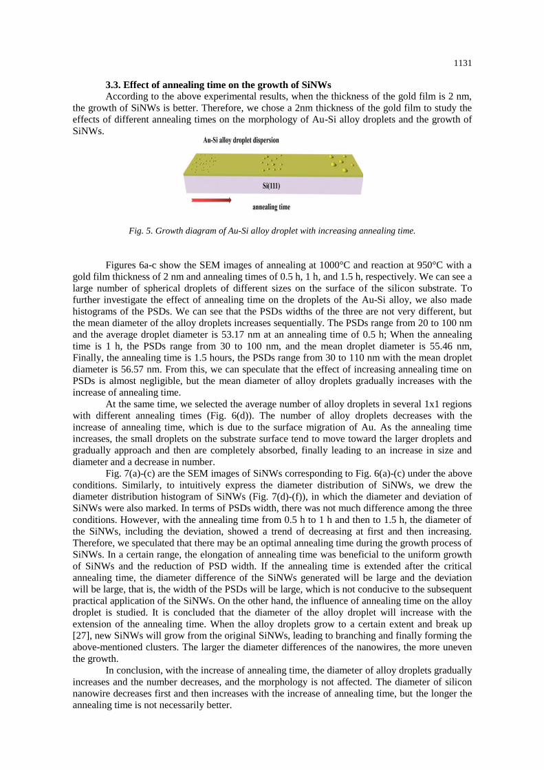
3.3. Effect of annealing time on the growth of SiNWs
According to the above experimental results, when the thickness of the gold film is 2 nm,
the growth of SiNWs is better. Therefore, we chose a 2nm thickness of the gold film to study the
effects of different annealing times on the morphology of Au-Si alloy droplets and the growth of
SiNWs.
Fig. 5. Growth diagram of Au-Si alloy droplet with increasing annealing time.
Figures 6a-c show the SEM images of annealing at 1000°C and reaction at 950°C with a
gold film thickness of 2 nm and annealing times of 0.5 h, 1 h, and 1.5 h, respectively. We can see a
large number of spherical droplets of different sizes on the surface of the silicon substrate. To
further investigate the effect of annealing time on the droplets of the Au-Si alloy, we also made
histograms of the PSDs. We can see that the PSDs widths of the three are not very different, but
the mean diameter of the alloy droplets increases sequentially. The PSDs range from 20 to 100 nm
and the average droplet diameter is 53.17 nm at an annealing time of 0.5 h; When the annealing
time is 1 h, the PSDs range from 30 to 100 nm, and the mean droplet diameter is 55.46 nm,
Finally, the annealing time is 1.5 hours, the PSDs range from 30 to 110 nm with the mean droplet
diameter is 56.57 nm. From this, we can speculate that the effect of increasing annealing time on
PSDs is almost negligible, but the mean diameter of alloy droplets gradually increases with the
increase of annealing time.
At the same time, we selected the average number of alloy droplets in several 1x1 regions
with different annealing times (Fig. 6(d)). The number of alloy droplets decreases with the
increase of annealing time, which is due to the surface migration of Au. As the annealing time
increases, the small droplets on the substrate surface tend to move toward the larger droplets and
gradually approach and then are completely absorbed, finally leading to an increase in size and
diameter and a decrease in number.
Fig. 7(a)-(c) are the SEM images of SiNWs corresponding to Fig. 6(a)-(c) under the above
conditions. Similarly, to intuitively express the diameter distribution of SiNWs, we drew the
diameter distribution histogram of SiNWs (Fig. 7(d)-(f)), in which the diameter and deviation of
SiNWs were also marked. In terms of PSDs width, there was not much difference among the three
conditions. However, with the annealing time from 0.5 h to 1 h and then to 1.5 h, the diameter of
the SiNWs, including the deviation, showed a trend of decreasing at first and then increasing.
Therefore, we speculated that there may be an optimal annealing time during the growth process of
SiNWs. In a certain range, the elongation of annealing time was beneficial to the uniform growth
of SiNWs and the reduction of PSD width. If the annealing time is extended after the critical
annealing time, the diameter difference of the SiNWs generated will be large and the deviation
will be large, that is, the width of the PSDs will be large, which is not conducive to the subsequent
practical application of the SiNWs. On the other hand, the influence of annealing time on the alloy
droplet is studied. It is concluded that the diameter of the alloy droplet will increase with the
extension of the annealing time. When the alloy droplets grow to a certain extent and break up
[27], new SiNWs will grow from the original SiNWs, leading to branching and finally forming the
above-mentioned clusters. The larger the diameter differences of the nanowires, the more uneven
the growth.
In conclusion, with the increase of annealing time, the diameter of alloy droplets gradually
increases and the number decreases, and the morphology is not affected. The diameter of silicon
nanowire decreases first and then increases with the increase of annealing time, but the longer the
annealing time is not necessarily better.

1132
Fig. 6. SEM images and PSD histograms of alloy droplet with different annealing time: (a) 0.5 h; (b)
1 h; (c) 1.5 h; (a΄),(b΄), and (c΄) correspond to a, b, and c; (d) Alloy droplet count in 1×1 cm
region(It is visible to the naked eye under this scale).

1133
Fig. 7. SEM images of SiNWs at different annealing time: (a)0.5h; (b)1h; (c)1.5h;
(d), (e), and (f) are histograms of PSD corresponding to (a), (b), and (c).
Table 1. The summary of the calculated specifications for Au-Si alloy droplets and SiNWs.
Annealing
time(h)
The average diameter
of SiNWs(nm)
The average diameter of
alloy droplet(nm)
the areal density of
alloy droplet(cm-2
)
0.5 92.47 53.17 59
1.0 61.25 55.46 33
1.5 69.87 56.57 21
We selected the samples annealed at 1000°C, reacted at 950°C, and the thickness of the
gold film was 2 nm, and the annealing time was 1.0 h for the following discussion.
Fig. 8(a) shows the Raman spectra of SiNWs obtained under this condition, which was
similar to bulk silicon materials. The main difference was in the frequency shift and half-peak
width, the spike shifted from 521 cm-1 to 512.4 cm-1, the half-peak width increased from 4 cm-1
to 6 cm-1, there were weak sub-peaks at 302 cm-1 and 964 cm-1, respectively, and the transverse
acoustic double-phonon peak of the bulk silicon material(2TA) and transverse optical two-photon
peak(2TO) scattering correspond to the primary cause of the red-shift, which was the phonon-
limiting effect of the nanocrystals, while the increase in half-peak width may be due to inter-lattice
mismatch and temperature determination.

1134
Fig. 8. Other characterization of SiNWs: (a) Raman; (b) XRD
Fig. 8(b) shows the XRD spectroscopy results of SiNWs, which shows that the resulting
SiNWs have a similar structure to bulk silicon materials, the main lattice directions are Si(111),
Si(220), and Si(311) at 28.5°, 47.4°, and 56.2° respectively, which differ from bulk silicon with a
broad peak of 0.136 nm near 21°, the phenomenon may be attributed to the surface oxidation of
SiNWs after synthesis and corresponds to the results of XRD spectra of silicon dioxide(SiO2) [28].
Fig. 9. (a) TEM image of SiNWs; (b) A magnified pattern of the specified region; (c) SAED model
was taken from (a); (d) EDX diagram of the SiNWs.
To further determine the crystal structure of SiNWs, the samples were characterized by
TEM. Fig 9a showed a typical high-magnification TEM image of the prepared SiNWs. Fig. 9(b)
was the local magnification of the single silicon nanowire, showing relatively uniform lattice
spacing. Combined with Fig. 9(c), it can be seen that the silicon nanowire was monocrystalline
silicon, mainly along the line of <111>; the direction grows with 0.323nm lattice spacing. The
EDX energy spectrum in Fig. 9(d) shows that the Si: O content of the samples are about 4:1,
indicating that the primary product produced was not silicon oxide. TEM images and EDX
analysis showed that the linear structure on the surface of the matrix was SiNWs. In our
experiment, no additional oxygen was provided. The main reasons for the appearance of oxygen
element in the EDX energy spectrum are as follow: First, the carrier gas contained a small amount

1135
of oxygen, which leaded to the oxidation of silicon crystals [29]; Secondly, the presence of trace
oxygen in the system caused the oxidation of the SiNWs. Due to the high surface activity of
SiNWs and the presence of a large number of suspension bonds, they were easily oxidized to
silicon oxide.
4. Conclusions
In the VLS process, we used SiCl4 as the precursor to prepare SiNWs under the conditions
of gold catalyst and annealing. The influence of gold film thickness on SiNWs, the influence of
annealing time on alloy droplets, and the influence of annealing time on SiNWs were
systematically studied. The conclusions are as follows: (ⅰ) The presence of catalyst and annealing
are necessary for the preparation of SiNWs by this method; (ⅱ) The diameter of SiNWs increases
with the increase of gold film thickness; (ⅲ) With the increase of annealing time, the diameter of
alloy droplets increases, but the number decreases, and the diameter of SiNWs decreases first and
then increases; (ⅳ) The reason why the SiNWs will aggregate in the growth process may be that
alloy droplets break when they reach a certain size, scattering small particles, forming a secondary
catalytic effect, and a lot of small new SiNWs will grow. As time goes by, more and more SiNWs
will aggregate gradually.
Acknowledgements
This work was supported by the National Natural Science Foundation of China (No.
2176060184), the Science and Technology Project of Guizhou Province (No. Qian Ke He Ping Tai
Ren Cai [2019] 5609), the Science and Technology Planning Project of Guizhou Province (Qian
Ke He Zhi Cheng [2021]Yiban 493), and GIT Academic Seedling Training and Innovation
Exploration Project (No. GZLGXM-11).
References
[1] R. Smith, S. M. Geary, A. K. Salem, ACS Appl. Nano Mater 3, 8522 (2020).
[2] M. O. Noor, U. J. Krull, Analytica Chimica Acta 825, 1 (2014).
[3] K. S. Chang, C. C. Chen, J. T. Sheu, Y. K. Li, Sensors & Actuators B Chemical 138(1),
148 (2009).
[4] M. W. Shao, L. Cheng, X. H. Zhang, D. D. D. Ma, S. T. Lee, Journal of the American
Chemical Society 131(49), 17738 (2009).
[5] R. Q. Zhang, X. M. Liu, Z. Wen, Q. Jiang, The Journal of Physical Chemistry C 115(8),
3425 (2011).
[6] A. F. Gonzalez, N. H. Yang, R. S. Liu, The Journal of Physical Chemistry C 121,
27775 (2017).
[7] Q. K. Shu, J. Q. Wei, K. L. Wang, H. W. Zhu, Z. Li, Y. Jia, X. C. Gui, N. Guo, X. Li,
C. R. Ma, D. H. Wu, Nano Letters 9(12), 4338 (2009).
[8] R. G. Treuting, S. M. Arnold, Acta Metallurgica 5(10), 598 (1957).
[9] R. S. Wagner, W. C. Ellis, K. A. Jackson, S. M. Arnold, Journal of Applied Physics 35(10),
2993 (1964).
[10] Sumio, Lijima, Nature 354(6348), 56 (1991).
[11] Hideo Namatsu, Seiji Horiguchi, Masao Nagase, Kenji Kurihara, Journal of vacuum science
and technology B 15(5), 1688 (1997).
[12] D. Ali, H. Ahmed, Applied Physics Letters 64(16), 2119 (1994).
[13] Takahitop Ono, Hiroaki Saitoh, Masayoshi Esashi, Applied Physics Letters 70(14),
1852 (1997).
[14] A. M. Morales, C. M. Lieber, Science 279(5348), 208 (1998).

1136
[15] Y. F. Zhang, Y. H. Tang, N. Wang, D. P. Yu, C. S. Lee, I. Bello, S. T. Lee, Applied Physics
Letters 72(15), 1835 (1998).
[16] Akitoshi lshizaka, Yasuhiro Shiraki, Journal of the Electrochemical Society 133, 666 (1986).
[17] R. Q. Zhang, Y. Lifshitz, S. T. Lee, Advanced Materials 15(78), 635 (2003).
[18] J. D. Holmes, K. P. Johnston, R. C. Doty, B. A. Korgel. Science 287(5457), 1471 (2000).
[19] Hiroshi Suzuki, Hiroshi Araki, Masahiro Tosa, Tetsuji Noda, Materials Transactions 48(8),
2202 (2007).
[20] Y. W. Wang, V. Schmidt, S. Senz, U. Gosele, Nature Nanotechnology 1(3), 186 (2006).
[21] J. Y. Yu, S. W. Chung, J. R. Heath, Journal of Physical Chemistry B 104(50), 11864 (2000).
[22] H. Y. Tuan, Ali Ghezelbash, B. A. Korgel, Chemistry of Materials 20(6), 2306 (2008).
[23] Minsung Jeon, Koichi Kamisako, Materials Letters 63(9-10), 777 (2009).
[24] E. C. Garnett, W. J. Liang, P. D. Yang, Advanced Materials 19, 2946 (2007).
[25] L. W. Yu, P. R. Cabarrocas, Physical Review B 80(8), 085313 (2009).
[26] J. B. Hannon, S. Kodambaka, F. M. Ross, R. M. Tromp, Nature 440, 69 (2006).
[27] K. Govatsi, A. Chrissanthopoulos, V. Dracopoulos, S. N. Yannopoulos, Nanotechnology
25(21), 215601 (2014).
[28] Y. H. Tang, Y. F. Zhang, C. S. Lee, N. Wang, D. P. Yu, I. Bello, S. T. Lee, Mrs Proceedings
526, 73 (1998).
[29] S. Kodambaka, J. B. Hannon, R. M. Tromp, F. M. Ross, Nano Letters 6(6), 1292 (2006).