Embed Size (px)
Citation preview
PROCEEDINGS OF THE INTERNATIONAL CONFERENCE
NANOMATERIALS: APPLICATIONS AND PROPERTIES
Vol. 2 No 1, 01PCSI29(6pp) (2013)
2304-1862/2013/2(1)01PCSI29(6) 01PCSI29-1 2013 Sumy State University
Effect of Film Thickness and Annealing on the Structural and Optical Properties
of CuInAlSe2 Thin Films
U. Parihar1, N. Padha1, J.R. Ray2, M.S. Desai2, C.J. Panchal2,*, P.K. Mehta3,
I.V. Cheshko4, I.Yu. Protsenko4
1 Department of Physics& Electronics, University of Jammu, Jammu-180006 J & K, India 2 Applied Physics Department, Faculty of Technology and Engineering, The M. S. University of Baroda, Vadodara-
390001, Gujarat, India 3 Physics Department, Faculty of Science, The M. S. University of Baroda, Vadodara-390002, Gujarat, India 4 Applied Physics Department, Faculty of Electronic and Informational Technologies, Sumy State University,
2, Rymskogo-Korsakova Str., 40007 Sumy, Ukraine
(Received 09 July 2013; published online 31 August 2013)
CuIn1 – xAlxSe2 (CIAS) thin films were grown using flash evaporation method by varying the film
thickness from 500 nm to 700 nm. Prepared CIAS thin films were annealed at 573 K for one hour in
vacuum. The influence of film’s thickness and the annealing temperature were characterized by the X-ray
diffraction (XRD), Scanning electron microscopy (SEM), Energy dispersive analysis of X-ray (EDAX),
Optical transmission measurements, and Hall Effect measurement. As the film thickness increases the
crystallinity improves and due to that the optical absorption also improves. The further improvement for
different thicknesses of CIAS thin films were observed by annealing. The thicker (700 nm) and annealed
CIAS thin film shows the crystallite size of 24.3 nm, energy band gap of 1.19 eV, and resistivity of about
9 102 Ω cm.
Keywords: Film system, CuInAlSe2, Optical properties, Scanning electron microscopy, Hall Effect.
PACS numbers: 61.05.C – 68.37.Lp, 78.66.Bz,
81.40.Gh
1. INTRODUCTION
Copper indium diselenide (CIS) and its alloys, CIAS and, CIASSe, shows its potential towards the
achievement of higher energy conversion efficiency at
lower fabrication cost in the area of thin film solar
cells [1, 2, 3]. The optical energy band gap of CIS in-creases by substituting Ga / Al for In and S for Se,
which is essential to enhance the photovoltaic conver-
sion efficiency in CIS based solar cells. For energy band gap greater than 1.3 eV the fill-factor and the
open-circuit voltage of the solar cell reduces due to the
degradation of the electronic properties of the absorb-
er [4]. Aluminum (Al) is easily available and less cost-ly compared to Gallium (Ga). By alloying of Al to CIS
the energy band gap changes from 1.0 eV (CIS) to
2.7 eV (CuAlSe2), which can absorb most of visible
radiation of solar spectrum. CuIn1 – xAlxSe2 (x 0.13)
single junction solar cell exhibited an efficiency of
16.9 % [5]. The tandem junction was proposed [6] to achieve higher photovoltaic conversion efficiency in
CuInSe2 based solar cells as the calculated energy
conversion efficiency for CIS (1.1 eV) / CIAS (1.7 eV) tandem cell was estimated to be 29 % [7]. CuIn1 –
xAlxSe2 (x 0.13) chalcopyrite material is prepared
and CIAS thin film of different thicknesses were grown by flash evaporation method. The post-
deposition annealing was carried out for the CIAS
thin film of different thicknesses. The influence of the film thickness variation and the annealing tempera-
ture were observed by different methods like XRD,
SEM, EDAX, optical transmission and electrical
measurements.
2. EXPERIMENT
CIAS thin films were deposited by flash evaporation
method on an organically cleaned, 3 mm thick, soda lime
glass substrate. The CIAS compound was prepared by
using the melt-quenching method, described elsewhere
[8]. The substrate temperature was kept constant, at
473 K, and varied the thickness of the CIAS thin film viz.
200 nm, 500 nm and 700 nm. The deposition rate was of
the order of 0.2-0.3 nms – 1 and the thickness of CIAS films
was measured using a quartz crystal thickness monitor
(Hind Hi Vac. DTM-101). The thermal annealing was car-
ried out for all the different thicknesses of CIAS thin films
at 573 K in rough vacuum for one hour.
All the deposited and annealed CIAS thin films were
characterized using HR-X-ray diffractometer (XRD)
(Bruker D8-Discover) in 2θ range 20-70 at a scan rate
0.02 s – 1 with Cu-Kα radiation source. The surface mor-
phology and chemical composition of the deposited thin
films was studied using scanning electron microscope
(Philips ESEM, 30XL) equipped with EDAX facilities
operated at 30 kV with standard ZAF quantification.
The CIAS thin films were also characterized for op-
tical measurement at room temperature using Hitachi
U3400 UV-VIS-NIR double beam spectrophotometer.
Hall measurements were done to verify the conductivi-
ty type, resistivity, mobility, and carrier concentration
of the deposited thin films.
3. RESULT
3.1 Structural Characterization
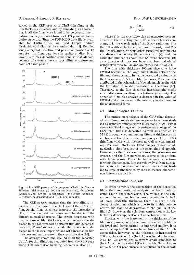
There is an obtrusive betterment was clearly ob-
U. PARIHAR, N. PADHA, J.R. RAY, ET AL. PROC. NAP 2, 01PCSI29 (2013)
01PCSI29-2
served in the XRD spectra of CIAS thin films as the
film thickness increases and by annealing, as shown in Fig. 1. All the films were found to be polycrystalline in
nature, majorly oriented towards (112) plane of chalco-pyrite structure. Since no PDF-ICDD data file is avail-
able for Cu(In, Al)Se2, we used Copper indium diselenide (CuInSe2) as the standard data [9]. Detailed
study of crystal structure and phase composition of Fe and Au thin films was done in earlier studies. It al-
lowed us to pick deposition conditions so that all com-ponents of systems have a crystalline structure and
have not oxide phases.
20 30 40 50 60 70
0
40
80
120
160
(a) 200nm(as-deposited)
Inte
nsity(a
rbitra
ry c
ou
nts
)
2 (Degrees)
0
40
80
120
160
(b) 200nm(Annealed)
0
50
100
150
200
(c) 500nm(as-deposited)
0
100
200
300
(d) 500nm(Annealed)
0
100
200
300
(e) 700nm(as-deposited)
0
100
200
300
(312/116)
(220/204)
(112)
(f) 700nm(Annealed)
Fig. 1 – The XRD pattern of the prepared CIAS thin films at
different thicknesses (a) 200 nm (as-deposited), (b) 200 nm
(annealed), (c) 500 nm (as-deposited), (d) 500 nm (annealed)
(e) 700 nm (as-deposited) and (f) 700 nm (annealed)
The XRD spectra suggest that the crystallinity in-
creases with increase in the thickness of the CIAS thin
film. As the films thickness increases the intensity of
(112) diffraction peak increases and the shape of the
diffraction peak sharpens. The strain decreases with
the increase of film thickness, which reflects the de-
crease in the cohesive force between film and substrate
material. Therefore, we conclude that there is a de-
crease in the lattice imperfections with increase in film
thickness and an increase in the crystallite size [10].
The average crystalline size (D) of all the deposited
CuInAlSe2 thin films was evaluated from the XRD peak
along (112) orientation by using Scherer’s relation [11]
0.9
cosD
(1)
where D is the crystallite size as measured perpen-
dicular to the reflecting plane, 0.9 is the Scherer’s con-
stant, is the wavelength of the X-ray radiation, is
the full width at half the maximum intensity, and is
the Bragg’s angle. Various other structural parameters
viz. dislocation density (δ), micro strain (ε), and the
estimated number of crystallites (N) were observed [12]
as a function of thickness have also been calculated
using relevant formulae and are presented in Table 1.
The film with thickness 200 nm showed a large
FWHM because of the large misfit strain between the
film and the substrate. Its value decreased gradually as
the thickness of CIAS thin film increases. This result is
attributed to the relaxation of the mismatch strain with
the formation of misfit dislocation in the films [13].
Therefore, as the film thickness increases, the misfit
strain decreases resulting in a better crystallinity. The
annealed films also showed a decrease in the value of
FWHM and an increase in the intensity as compared to
the as-deposited films.
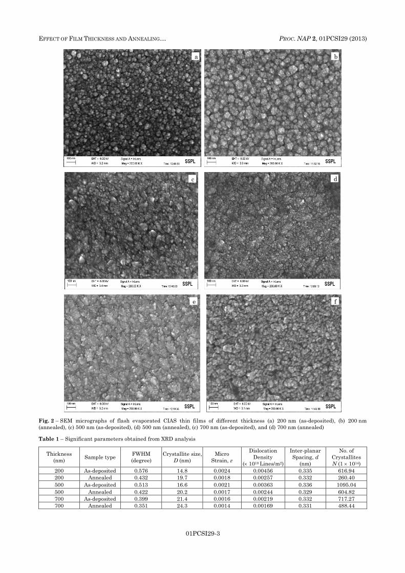
3.2 Morphological Studies
The surface morphologies of the CIAS films deposit-
ed at different substrate temperatures have been stud-
ied by using scanning electron microscope (SEM). Fig. 2
shows the SEM images of the surface morphology of the
CIAS thin films as-deposited as well as annealed at
573 K in rough vacuum, having different thicknesses. It
is observed that the surface morphology of the CIAS
thin films varies with thickness as well as with anneal-
ing. For small thickness, SEM images present small
nucleation sites because of the short time of growth.
However, as the thickness increases, the grain size in-
creases, and the film morphology seems to be uniform
with large grains. From the fundamental structure-
forming phenomenon, film growth evolves from nuclea-
tion islands to the growth of the continuous films, lead-
ing to large grains formed by the coalescence phenome-
non between grains [14].
3.3 Compositional Analysis
In order to verify the composition of the deposited
films, their compositional analysis has been made by
using EDAX characterization. The values of the con-
stituent elements so obtained are presented in Table 2.
At lower CIAS film thickness, there has been a defi-
ciency of selenium, which is due to its highly volatile
nature and leads to degradation of the quality of the
film [15]. However, the selenium composition is the key
factor for device applications of undertaken films.
Further, with the increment in the thickness of the
film an improvement of selenium content in the film is
observed and demonstrated its improved quality. It is
seen that up to 500 nm we have observed the Cu-rich
composition, however, as the thickness is increased to
700 nm, the ratio of Cu / (In + Al) was found to be about
0.73, i.e. Cu atoms are relatively small compared to
(In + Al) while the ratio of (Cu + In + Al) / Se is close to
unity. Since Cu-poor surface is beneficial for the overall
EFFECT OF FILM THICKNESS AND ANNEALING… PROC. NAP 2, 01PCSI29 (2013)
01PCSI29-3
Fig. 2 – SEM micrographs of flash evaporated CIAS thin films of different thickness (a) 200 nm (as-deposited), (b) 200 nm
(annealed), (c) 500 nm (as-deposited), (d) 500 nm (annealed), (c) 700 nm (as-deposited), and (d) 700 nm (annealed)
Table 1 – Significant parameters obtained from XRD analysis
Thickness
(nm) Sample type
FWHM
(degree)
Crystallite size,
D (nm)
Micro
Strain, ε
Dislocation
Density
( 1010 Lines/m2)
Inter-planar
Spacing, d
(nm)
No. of
Crystallites
N (1 1014)
200 As-deposited 0.576 14.8 0.0024 0.00456 0.335 616.94
200 Annealed 0.432 19.7 0.0018 0.00257 0.332 260.40
500 As-deposited 0.513 16.6 0.0021 0.00363 0.336 1095.04
500 Annealed 0.422 20.2 0.0017 0.00244 0.329 604.82
700 As-deposited 0.399 21.4 0.0016 0.00219 0.332 717.27
700 Annealed 0.351 24.3 0.0014 0.00169 0.331 488.44
а b
c d
e f
U. PARIHAR, N. PADHA, J.R. RAY, ET AL. PROC. NAP 2, 01PCSI29 (2013)
01PCSI29-4
performance of the film for device application [16]. Fur-
ther, it has been noted that annealing of the films im-
proves their quality. However, thickness beyond
700 nm caused re-evaporation of selenium, thus, con-
firming 700 nm thick film suits to various device appli-
cations.
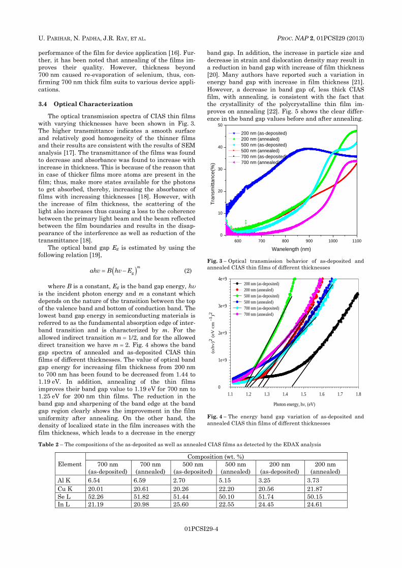
3.4 Optical Characterization
The optical transmission spectra of CIAS thin films
with varying thicknesses have been shown in Fig. 3.
The higher transmittance indicates a smooth surface
and relatively good homogeneity of the thinner films
and their results are consistent with the results of SEM
analysis [17]. The transmittance of the films was found
to decrease and absorbance was found to increase with
increase in thickness. This is because of the reason that
in case of thicker films more atoms are present in the
film; thus, make more states available for the photons
to get absorbed, thereby, increasing the absorbance of
films with increasing thicknesses [18]. However, with
the increase of film thickness, the scattering of the
light also increases thus causing a loss to the coherence
between the primary light beam and the beam reflected
between the film boundaries and results in the disap-
pearance of the interference as well as reduction of the
transmittance [18].
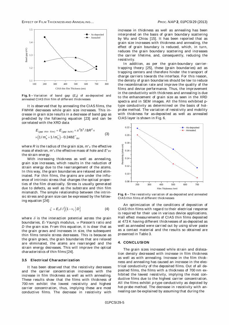
The optical band gap Eg is estimated by using the
following relation [19],
g
mαhυ B hυ E (2)
where B is a constant, Eg is the band gap energy, h
is the incident photon energy and m a constant which
depends on the nature of the transition between the top
of the valence band and bottom of conduction band. The
lowest band gap energy in semiconducting materials is
referred to as the fundamental absorption edge of inter-
band transition and is characterized by m. For the
allowed indirect transition m 1/2, and for the allowed
direct transition we have m 2. Fig. 4 shows the band
gap spectra of annealed and as-deposited CIAS thin
films of different thicknesses. The value of optical band
gap energy for increasing film thickness from 200 nm
to 700 nm has been found to be decreased from 1.44 to
1.19 eV. In addition, annealing of the thin films
improves their band gap value to 1.19 eV for 700 nm to
1.25 eV for 200 nm thin films. The reduction in the
band gap and sharpening of the band edge at the band
gap region clearly shows the improvement in the film
uniformity after annealing. On the other hand, the
density of localized state in the film increases with the
film thickness, which leads to a decrease in the energy
band gap. In addition, the increase in particle size and
decrease in strain and dislocation density may result in
a reduction in band gap with increase of film thickness
[20]. Many authors have reported such a variation in
energy band gap with increase in film thickness [21].
However, a decrease in band gap of, less thick CIAS
film, with annealing, is consistent with the fact that
the crystallinity of the polycrystalline thin film im-
proves on annealing [22]. Fig. 5 shows the clear differ-
ence in the band gap values before and after annealing.
600 700 800 900 1000 1100
0
10
20
30
40
50
Tra
nsm
itta
nce
(%)
Wanelength (nm)
200 nm (as-deposited)
200 nm (annealed)
500 nm (as-deposited)
500 nm (annealed)
700 nm (as-deposited)
700 nm (annealed)
Fig. 3 – Optical transmission behavior of as-deposited and
annealed CIAS thin films of different thicknesses
Photon energy, h(eV)
1.1 1.2 1.3 1.4 1.5 1.6 1.7 1.8
( h
)2 (
eV
cm
-1)2
0
1e+9
2e+9
3e+9
4e+9200 nm (as-deposited)
200 nm (annealed)
500 nm (as-deposited)
500 nm (annealed)
700 nm (as-deposited)
700 nm (annealed)
Fig. 4 – The energy band gap variation of as-deposited and
annealed CIAS thin films of different thicknesses
Table 2 – The compositions of the as-deposited as well as annealed CIAS films as detected by the EDAX analysis
Element
Composition (wt. %)
700 nm
(as-deposited)
700 nm
(annealed)
500 nm
(as-deposited)
500 nm
(annealed)
200 nm
(as-deposited)
200 nm
(annealed)
Al K 6.54 6.59 2.70 5.15 3.25 3.73
Cu K 20.01 20.61 20.26 22.20 20.56 21.87
Se L 52.26 51.82 51.44 50.10 51.74 50.15
In L 21.19 20.98 25.60 22.55 24.45 24.61
EFFECT OF FILM THICKNESS AND ANNEALING… PROC. NAP 2, 01PCSI29 (2013)
01PCSI29-5
CIAS thin film Thickness (nm)
100 200 300 400 500 600 700 800
Band
gap
(eV
)
1.1
1.2
1.3
1.4
1.5
As-depositedAnnealed
Fig. 5 – Variation of band gap (Eg) of as-deposited andannealed CIAS thin film of different thicknesses
It is observed that by annealing the CIAS films, theFWHM decreases while grain size increases. This in-crease in grain size results in a decrease of band gap aspredicted by the following equation [23] and can becorrelated with the XRD data
2 2 2( ) ( )
* * *RY
/ 8
1 / 1 / 0.248gap thin film gap bulk
e h
E E h R
m m E(3)
where R is the radius of the grain size, m*e the effectivemass of electron, m*h the effective mass of hole and E*RYthe strain energy.
With increasing thickness as well as annealing,grain size increases, which results in the reduction ofstrain energy due to the rearrangement of the atoms.In this way, the grain boundaries are relaxed and elim-inated. For thin films, the grains are under the influ-ence of intrinsic stress that changes the optical proper-ties of the film drastically. Stress is usually generateddue to defects, as well as the substrate and thin filmmismatch. The simple relationship between the intrin-sic stress and grain size can be expressed by the follow-ing equation [24]:
f / 1 fE D (4)
where is the interaction potential across the grainboundaries, Ef Young’s modulus, f Poisson’s ratio andD the grain size. From this equation, it is clear that asthe grain grows and increases in size, the subsequentthin films tensile stress decreases. This is because asthe grain grows, the grain boundaries that are relaxedare eliminated, the atoms are rearranged and thestrain energy decreases. This will improve the opticalcharacteristics of thin films [24].
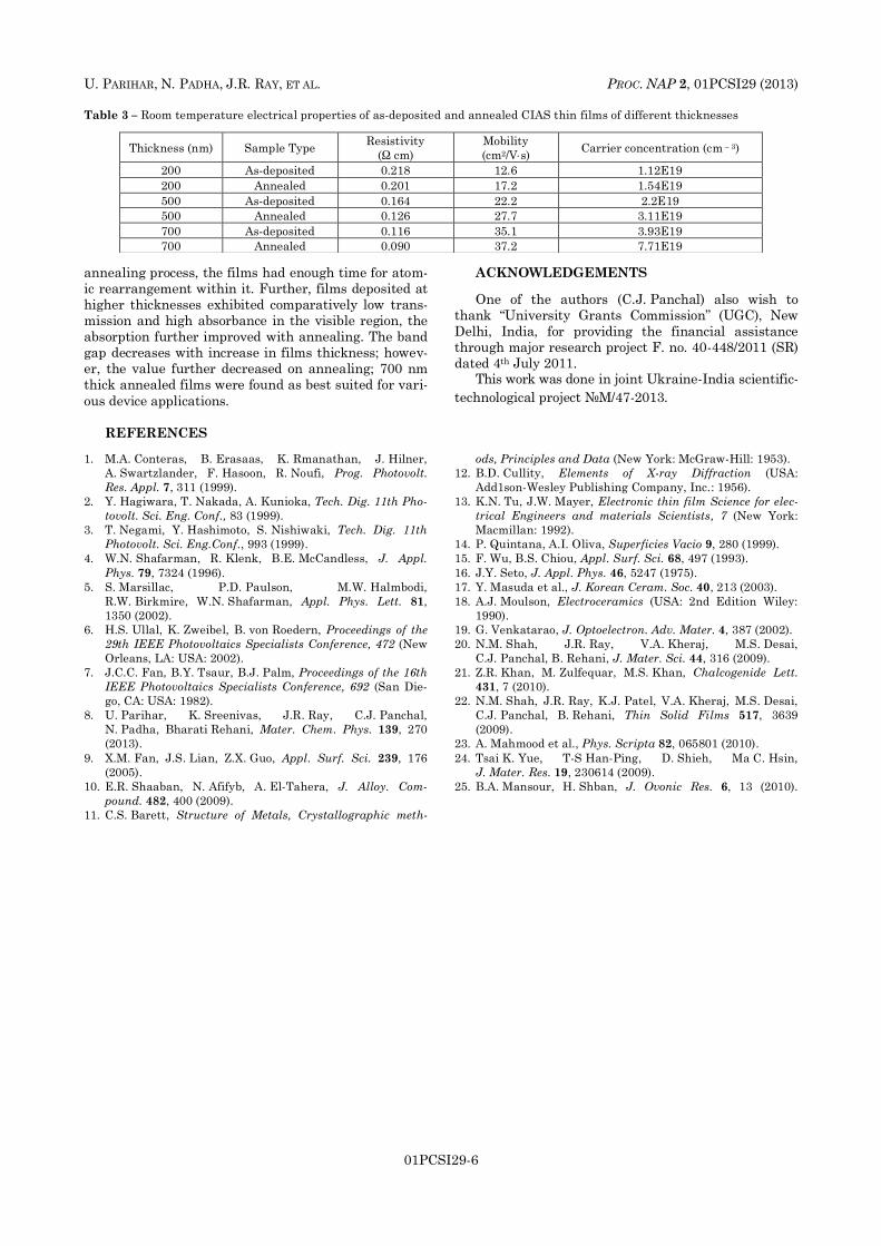
3.5 Electrical Characterization
It has been observed that the resistivity decreasesand the carrier concentration increases with theincrease in film thickness as well as with annealing.These results show that the films with thickness of700 nm exhibit the lowest resistivity and highestcarrier concentration, thus, implying these are mostconductive films. The decrease in resistivity with
increase in thickness as well as annealing has beeninterpreted on the basis of grain boundary scatteringby Wu and Chiou [15]. It has been reported that asgrain size increases with thickness and annealing, theeffect of grain boundary is reduced, which, in turn,reduces the grain boundary scattering and increasesthe carrier lifetime, and, consequently, reducing theresistivity.
In addition, as per the grain-boundary carrier-trapping theory [25], these (grain boundaries) act astrapping centers and therefore hinder the transport ofcharge carriers towards the interface. For this reason,the density of grain boundaries should be low to reducethe recombination rate and improve the quality of thefilms and device performance. Thus, the improvementin the conductivity with thickness and annealing is dueto the enhancement of grain size as seen in the XRDspectra and in SEM images. All the films exhibited p-type conductivity as determiined on the basis of hot-probe method. The variation of resistivity and mobilitywith thickness for as-deposited as well as annealedCIAS layer is shown in Fig. 6.
200 300 400 500 600 7000.08
0.10
0.12
0.14
0.16
0.18
0.20
0.22
Res
istiv
ity(o
hm-c
m)
Film Thickness (nm)
As-depsoited Annealed
Fig. 6 – The resistivity variation of as-deposited and annealedCIAS thin films of different thicknesses
An optimization of the conditions of deposition ofCIAS thin films with regard to their electrical responseis required for their use in various device applications.Hall effect measurements of CIAS thin films depositedat 473 K having different thicknesses of as-deposited aswell as annealed were carried out by using silver pasteas a contact material and the results so obtained arepresented in Table 3.
4. CONCLUSION
The grain sizes increased while strain and disloca-tion density decreased with increase in film thicknessas well as with annealing. Increase in the film thick-ness and annealing has caused an increase in the elec-trical conductivity of the deposited films. Out of all de-posited films, the films with a thickness of 700 nm ex-hibited the lowest resistivity, implying the most con-ductive films due to the highest carrier concentration.All the films exhibit p-type conductivity as depicted byhot-probe method. The decrease in resistivity with an-nealing can be explained by assuming that during the
U. PARIHAR, N. PADHA, J.R. RAY, ET AL. PROC. NAP 2, 01PCSI29 (2013)
01PCSI29-6
Table 3 – Room temperature electrical properties of as-deposited and annealed CIAS thin films of different thicknesses
annealing process, the films had enough time for atom-
ic rearrangement within it. Further, films deposited at
higher thicknesses exhibited comparatively low trans-
mission and high absorbance in the visible region, the
absorption further improved with annealing. The band
gap decreases with increase in films thickness; howev-
er, the value further decreased on annealing; 700 nm
thick annealed films were found as best suited for vari-
ous device applications.
ACKNOWLEDGEMENTS
One of the authors (C.J. Panchal) also wish to
thank “University Grants Commission” (UGC), New
Delhi, India, for providing the financial assistance
through major research project F. no. 40-448/2011 (SR)
dated 4th July 2011. This work was done in joint Ukraine-India scientific-
technological project №M/47-2013.
REFERENCES
1. M.A. Conteras, B. Erasaas, K. Rmanathan, J. Hilner,
A. Swartzlander, F. Hasoon, R. Noufi, Prog. Photovolt.
Res. Appl. 7, 311 (1999).
2. Y. Hagiwara, T. Nakada, A. Kunioka, Tech. Dig. 11th Pho-
tovolt. Sci. Eng. Conf., 83 (1999).
3. T. Negami, Y. Hashimoto, S. Nishiwaki, Tech. Dig. 11th
Photovolt. Sci. Eng.Conf., 993 (1999).
4. W.N. Shafarman, R. Klenk, B.E. McCandless, J. Appl.
Phys. 79, 7324 (1996).
5. S. Marsillac, P.D. Paulson, M.W. Halmbodi,
R.W. Birkmire, W.N. Shafarman, Appl. Phys. Lett. 81,
1350 (2002).
6. H.S. Ullal, K. Zweibel, B. von Roedern, Proceedings of the
29th IEEE Photovoltaics Specialists Conference, 472 (New
Orleans, LA: USA: 2002).
7. J.C.C. Fan, B.Y. Tsaur, B.J. Palm, Proceedings of the 16th
IEEE Photovoltaics Specialists Conference, 692 (San Die-
go, CA: USA: 1982).
8. U. Parihar, K. Sreenivas, J.R. Ray, C.J. Panchal,
N. Padha, Bharati Rehani, Mater. Chem. Phys. 139, 270
(2013).
9. X.M. Fan, J.S. Lian, Z.X. Guo, Appl. Surf. Sci. 239, 176
(2005).
10. E.R. Shaaban, N. Afifyb, A. El-Tahera, J. Alloy. Com-
pound. 482, 400 (2009).
11. C.S. Barett, Structure of Metals, Crystallographic meth-
ods, Principles and Data (New York: McGraw-Hill: 1953).
12. B.D. Cullity, Elements of X-ray Diffraction (USA:
Add1son-Wesley Publishing Company, Inc.: 1956).
13. K.N. Tu, J.W. Mayer, Electronic thin film Science for elec-
trical Engineers and materials Scientists, 7 (New York:
Macmillan: 1992).
14. P. Quintana, A.I. Oliva, Superficies Vacio 9, 280 (1999).
15. F. Wu, B.S. Chiou, Appl. Surf. Sci. 68, 497 (1993).
16. J.Y. Seto, J. Appl. Phys. 46, 5247 (1975).
17. Y. Masuda et al., J. Korean Ceram. Soc. 40, 213 (2003).
18. A.J. Moulson, Electroceramics (USA: 2nd Edition Wiley:
1990).
19. G. Venkatarao, J. Optoelectron. Adv. Mater. 4, 387 (2002).
20. N.M. Shah, J.R. Ray, V.A. Kheraj, M.S. Desai,
C.J. Panchal, B. Rehani, J. Mater. Sci. 44, 316 (2009).
21. Z.R. Khan, M. Zulfequar, M.S. Khan, Chalcogenide Lett.
431, 7 (2010).
22. N.M. Shah, J.R. Ray, K.J. Patel, V.A. Kheraj, M.S. Desai,
C.J. Panchal, B. Rehani, Thin Solid Films 517, 3639
(2009).
23. A. Mahmood et al., Phys. Scripta 82, 065801 (2010).
24. Tsai K. Yue, T-S Han-Ping, D. Shieh, Ma C. Hsin,
J. Mater. Res. 19, 230614 (2009).
25. B.A. Mansour, H. Shban, J. Ovonic Res. 6, 13 (2010).
Thickness (nm) Sample Type Resistivity
(Ω cm)
Mobility
(cm2/Vs) Carrier concentration (cm – 3)
200 As-deposited 0.218 12.6 1.12E19
200 Annealed 0.201 17.2 1.54E19
500 As-deposited 0.164 22.2 2.2E19
500 Annealed 0.126 27.7 3.11E19
700 As-deposited 0.116 35.1 3.93E19
700 Annealed 0.090 37.2 7.71E19