Embed Size (px)
Citation preview
92
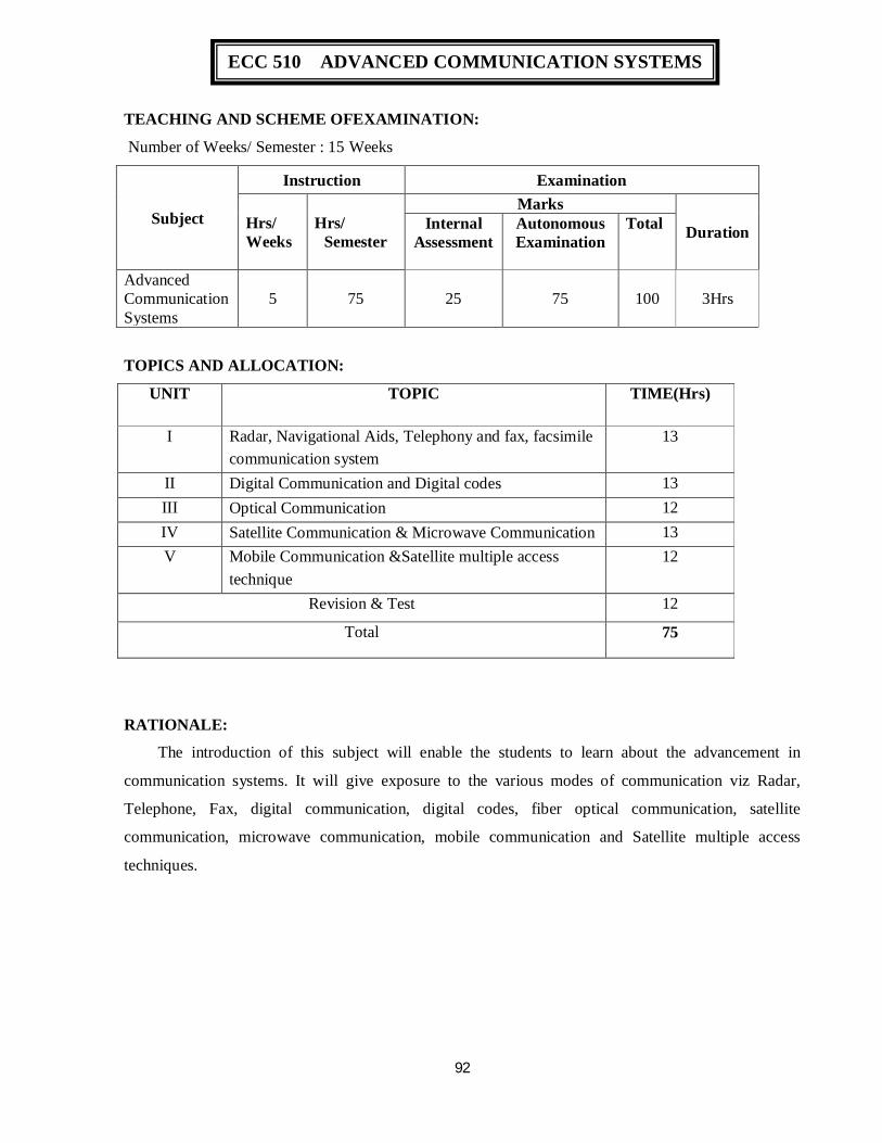
TEACHING AND SCHEME OFEXAMINATION:
Number of Weeks/ Semester : 15 Weeks
Subject
Instruction Examination
Hrs/ Weeks
Hrs/ Semester
Marks
Duration Internal Assessment
Autonomous Examination
Total
Advanced Communication Systems
5 75 25 75 100 3Hrs
TOPICS AND ALLOCATION:
UNIT TOPIC TIME(Hrs)
I Radar, Navigational Aids, Telephony and fax, facsimile communication system
13
II Digital Communication and Digital codes 13 III Optical Communication 12 IV Satellite Communication & Microwave Communication 13 V Mobile Communication &Satellite multiple access
technique 12
Revision & Test 12
Total 75
RATIONALE:
The introduction of this subject will enable the students to learn about the advancement in
communication systems. It will give exposure to the various modes of communication viz Radar,
Telephone, Fax, digital communication, digital codes, fiber optical communication, satellite
communication, microwave communication, mobile communication and Satellite multiple access
techniques.
ECC 510 ADVANCED COMMUNICATION SYSTEMS
93
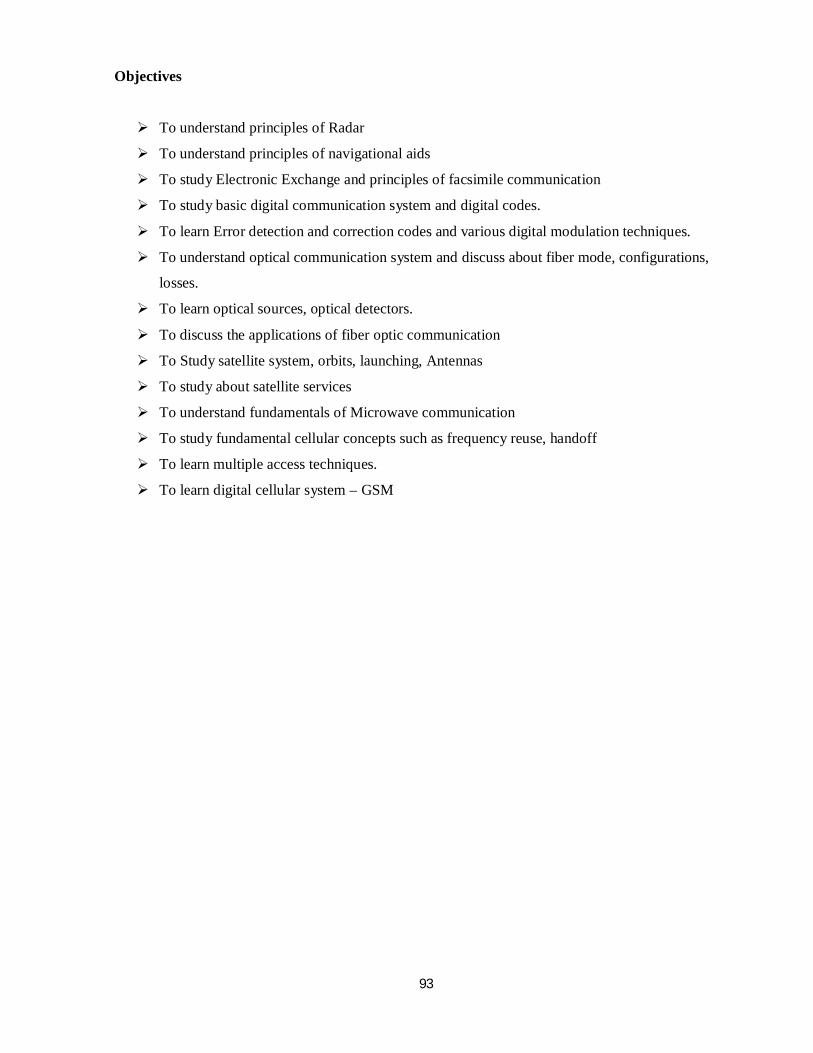
Objectives
To understand principles of Radar
To understand principles of navigational aids
To study Electronic Exchange and principles of facsimile communication
To study basic digital communication system and digital codes.
To learn Error detection and correction codes and various digital modulation techniques.
To understand optical communication system and discuss about fiber mode, configurations,
losses.
To learn optical sources, optical detectors.
To discuss the applications of fiber optic communication
To Study satellite system, orbits, launching, Antennas
To study about satellite services
To understand fundamentals of Microwave communication
To study fundamental cellular concepts such as frequency reuse, handoff
To learn multiple access techniques.
To learn digital cellular system – GSM
94
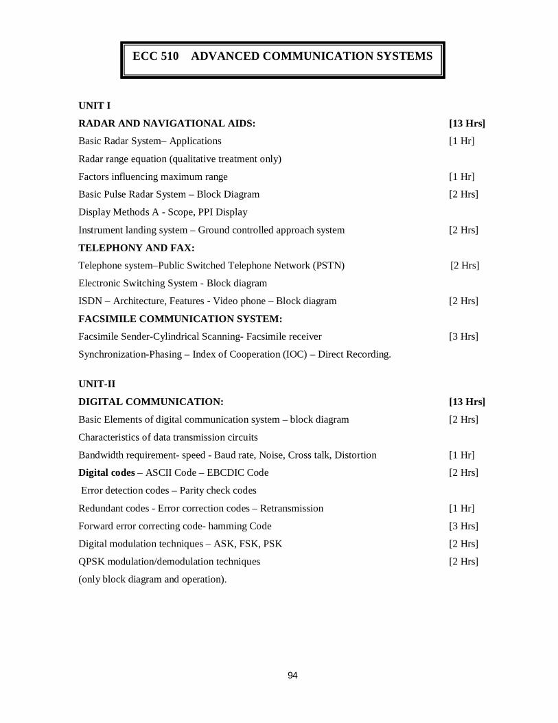
UNIT I
RADAR AND NAVIGATIONAL AIDS: [13 Hrs]
Basic Radar System– Applications [1 Hr]
Radar range equation (qualitative treatment only)
Factors influencing maximum range [1 Hr]
Basic Pulse Radar System – Block Diagram [2 Hrs]
Display Methods A - Scope, PPI Display
Instrument landing system – Ground controlled approach system [2 Hrs]
TELEPHONY AND FAX:
Telephone system–Public Switched Telephone Network (PSTN) [2 Hrs]
Electronic Switching System - Block diagram
ISDN – Architecture, Features - Video phone – Block diagram [2 Hrs]
FACSIMILE COMMUNICATION SYSTEM:
Facsimile Sender-Cylindrical Scanning- Facsimile receiver [3 Hrs]
Synchronization-Phasing – Index of Cooperation (IOC) – Direct Recording.
UNIT-II
DIGITAL COMMUNICATION: [13 Hrs]
Basic Elements of digital communication system – block diagram [2 Hrs]
Characteristics of data transmission circuits
Bandwidth requirement- speed - Baud rate, Noise, Cross talk, Distortion [1 Hr]
Digital codes – ASCII Code – EBCDIC Code [2 Hrs]
Error detection codes – Parity check codes
Redundant codes - Error correction codes – Retransmission [1 Hr]
Forward error correcting code- hamming Code [3 Hrs]
Digital modulation techniques – ASK, FSK, PSK [2 Hrs]
QPSK modulation/demodulation techniques [2 Hrs]
(only block diagram and operation).
ECC 510 ADVANCED COMMUNICATION SYSTEMS

95
UNIT-III
OPTICAL COMMUNICATION: [12 Hrs]
Optical Communication System– Block diagram [2 Hrs]
Advantages of optical fiber Communication systems
Principles of light transmission in a fiber using Ray Theory [2 Hrs]
Single mode fibers, multimode fibers
Step index fibers, graded index fibers (basic concepts only) [2 Hrs]
Attenuation in optical fibers – Absorption losses
Scattering losses, bending losses, core and cladding losses [2 Hrs]
Optical sources – LED - semiconductor LASER – Principles
Optical detectors – PIN and APD diodes [2 Hrs]
Connectors - Splices – Couplers
Optical transmitter – Block diagram – optical receiver Block diagram [2 Hrs]
Application of optical fibers – Networking, Industry and Military applications.
WDM – OTDR (Block diagram and Explanation only)
UNIT-IV
SATELLITE COMMUNICATION: [13 Hrs]
Satellite system: Kepler’s I,II,III laws – orbits – launching orbits - types [2 Hrs]
Geostationary synchronous satellites- Advantage
Apogee -Perigee- Active and passive satellite - Earth eclipse of satellite
Antenna: Parabolic reflector antenna - cassegrain antenna - Space segment [2 Hrs]
power supply- Attitude control [1Hr]
station keeping - Transponders – TT and C subsystem - Antenna Subsystem [1Hr] Earth segment—Block diagram of Transmit receive earth station [2 Hrs]
Satellite mobile services - Basics of GPS
MICROWAVE COMMUNICATION:
Microwave frequency ranges [2 Hrs]
Microwave devices – Parametric amplifiers
Travelling wave tubes –simple block diagram of microwave transmitter, [2 Hrs]
receiver and microwave link repeater.
Reflex Klystron – Magnetron - TWT [1Hr]
96
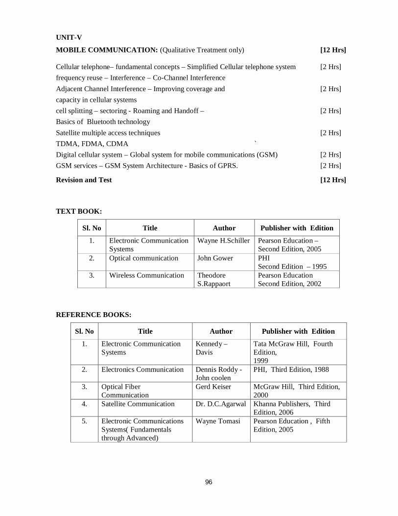
UNIT-V
MOBILE COMMUNICATION: (Qualitative Treatment only) [12 Hrs] Cellular telephone– fundamental concepts – Simplified Cellular telephone system [2 Hrs] frequency reuse – Interference – Co-Channel Interference Adjacent Channel Interference – Improving coverage and [2 Hrs] capacity in cellular systems cell splitting – sectoring - Roaming and Handoff – [2 Hrs] Basics of Bluetooth technology Satellite multiple access techniques [2 Hrs] TDMA, FDMA, CDMA ` Digital cellular system – Global system for mobile communications (GSM) [2 Hrs] GSM services – GSM System Architecture - Basics of GPRS. [2 Hrs]
Revision and Test [12 Hrs] TEXT BOOK: REFERENCE BOOKS:
Sl. No Title Author Publisher with Edition
1. Electronic Communication Systems
Wayne H.Schiller Pearson Education – Second Edition, 2005
2. Optical communication John Gower PHI Second Edition – 1995
3. Wireless Communication Theodore S.Rappaort
Pearson Education Second Edition, 2002
Sl. No Title Author Publisher with Edition
1. Electronic Communication Systems
Kennedy – Davis
Tata McGraw Hill, Fourth Edition, 1999
2. Electronics Communication Dennis Roddy -John coolen
PHI, Third Edition, 1988
3. Optical Fiber Communication
Gerd Keiser McGraw Hill, Third Edition, 2000
4. Satellite Communication Dr. D.C.Agarwal Khanna Publishers, Third Edition, 2006
5. Electronic Communications Systems( Fundamentals through Advanced)
Wayne Tomasi Pearson Education , Fifth Edition, 2005
97
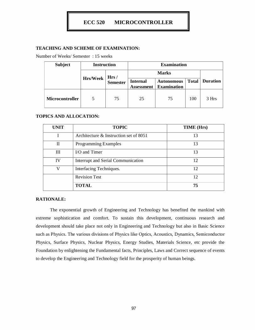
TEACHING AND SCHEME OF EXAMINATION:
Number of Weeks/ Semester : 15 weeks
Subject Instruction Examination
Hrs/Week Hrs / Semester
Marks
Duration Internal Assessment
Autonomous Examination
Total
Microcontroller 5
75 25 75 100 3 Hrs
TOPICS AND ALLOCATION:
UNIT TOPIC TIME (Hrs)
I Architecture & Instruction set of 8051 13
II Programming Examples 13
III I/O and Timer 13
IV Interrupt and Serial Communication 12
V Interfacing Techniques. 12
Revision Test 12
TOTAL 75
RATIONALE: The exponential growth of Engineering and Technology has benefited the mankind with
extreme sophistication and comfort. To sustain this development, continuous research and
development should take place not only in Engineering and Technology but also in Basic Science
such as Physics. The various divisions of Physics like Optics, Acoustics, Dynamics, Semiconductor
Physics, Surface Physics, Nuclear Physics, Energy Studies, Materials Science, etc provide the
Foundation by enlightening the Fundamental facts, Principles, Laws and Correct sequence of events
to develop the Engineering and Technology field for the prosperity of human beings.
ECC 520 MICROCONTROLLER
98
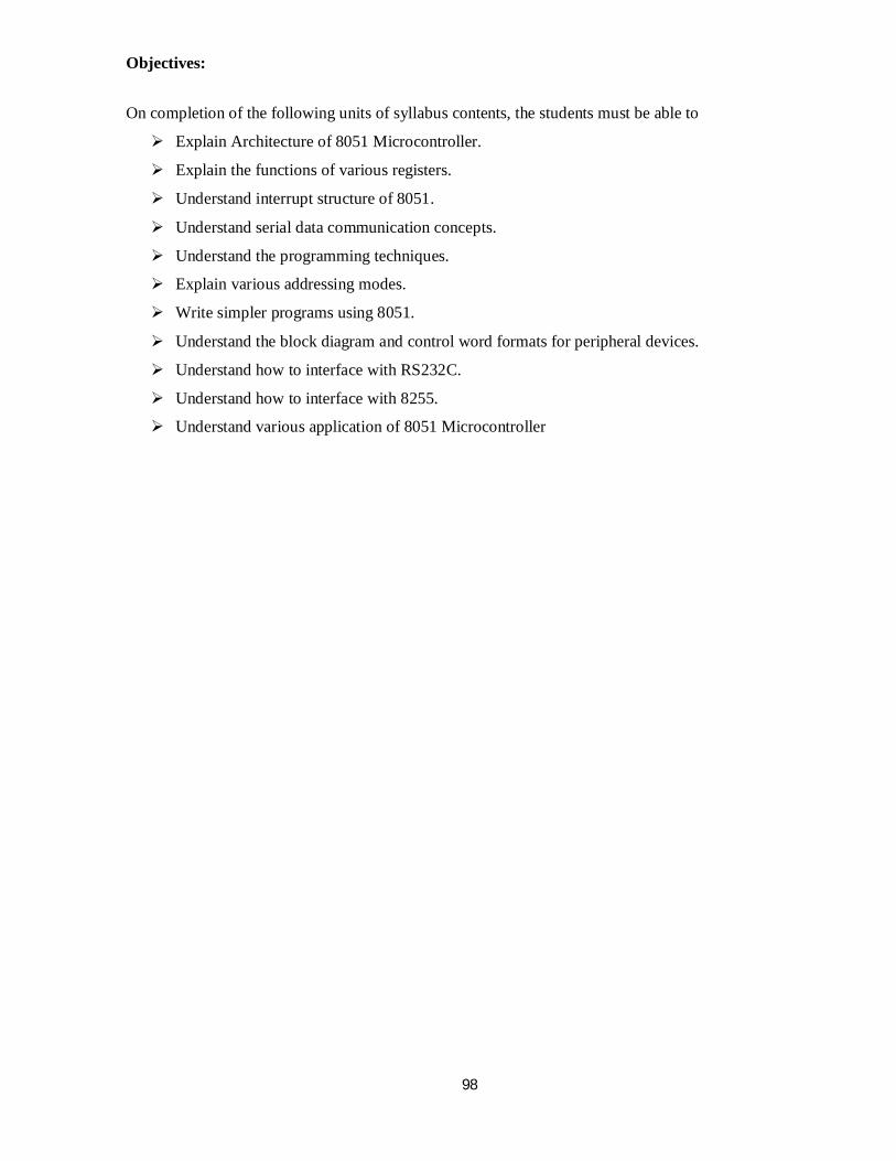
Objectives:
On completion of the following units of syllabus contents, the students must be able to
Explain Architecture of 8051 Microcontroller.
Explain the functions of various registers.
Understand interrupt structure of 8051.
Understand serial data communication concepts.
Understand the programming techniques.
Explain various addressing modes.
Write simpler programs using 8051.
Understand the block diagram and control word formats for peripheral devices.
Understand how to interface with RS232C.
Understand how to interface with 8255.
Understand various application of 8051 Microcontroller
99
UNIT – I
ARCHITECTURE & INSTRUCTION SET OF 8051: [13Hrs]
Comparison of Microprocessor and Microcontroller [2 Hrs]
Block diagram of Microcontroller – Functions of each block –
Pin details of 8051 [1 Hr]
ALU – ROM – RAM – Memory Organization of 8051
Special function registers – Program Counter – PSW register [2 Hrs]
Stack - I/O Ports – Timer – Interrupt – Serial Port [1 Hr]
Oscillator and Clock – Clock Cycle – State - Machine Cycle – Instruction cycle [2 Hrs]
Reset – Power on Reset – Overview of 8051 Family
Instruction set of 8051 – Classification of 8051 Instructions [2 Hrs]
Data transfer Instructions – Arithmetic Instructions – Logical Instructions [2 Hrs]
Branching Instructions – Bit Manipulation Instructions. [1 Hr]
UNIT – II
PROGRAMMING EXAMPLES: [13 Hrs]
Assembler and addressing modes
Assembling and running an 8051 program [1 Hr]
Structure of Assembly Language – Assembler directives [1 Hr]
Different addressing modes of 8051 – Programmes – Multibyte Addition [2 Hrs]
8 Bit Multiplication and Division [1 Hr]
Biggest Number / Smallest Number – Ascending order / Descending order [2 Hrs]
BCD to HEX Conversion – HEX to BCD Conversion [2 Hrs]
BCD to ASCII Conversion – ASCII to Binary Conversion [2 Hrs]
Odd Parity Generator - even Parity Generator – Time delay routines. [2 Hrs]
ECC 520 MICROCONTROLLER
100
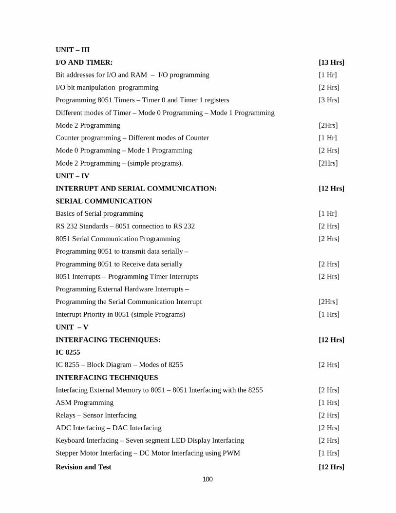
UNIT – III
I/O AND TIMER: [13 Hrs]
Bit addresses for I/O and RAM – I/O programming [1 Hr]
I/O bit manipulation programming [2 Hrs]
Programming 8051 Timers – Timer 0 and Timer 1 registers [3 Hrs]
Different modes of Timer – Mode 0 Programming – Mode 1 Programming
Mode 2 Programming [2Hrs]
Counter programming – Different modes of Counter [1 Hr]
Mode 0 Programming – Mode 1 Programming [2 Hrs]
Mode 2 Programming – (simple programs). [2Hrs]
UNIT – IV
INTERRUPT AND SERIAL COMMUNICATION: [12 Hrs]
SERIAL COMMUNICATION
Basics of Serial programming [1 Hr]
RS 232 Standards – 8051 connection to RS 232 [2 Hrs]
8051 Serial Communication Programming [2 Hrs]
Programming 8051 to transmit data serially –
Programming 8051 to Receive data serially [2 Hrs]
8051 Interrupts – Programming Timer Interrupts [2 Hrs]
Programming External Hardware Interrupts –
Programming the Serial Communication Interrupt [2Hrs]
Interrupt Priority in 8051 (simple Programs) [1 Hrs]
UNIT – V
INTERFACING TECHNIQUES: [12 Hrs]
IC 8255
IC 8255 – Block Diagram – Modes of 8255 [2 Hrs]
INTERFACING TECHNIQUES
Interfacing External Memory to 8051 – 8051 Interfacing with the 8255 [2 Hrs]
ASM Programming [1 Hrs]
Relays – Sensor Interfacing [2 Hrs]
ADC Interfacing – DAC Interfacing [2 Hrs]
Keyboard Interfacing – Seven segment LED Display Interfacing [2 Hrs]
Stepper Motor Interfacing – DC Motor Interfacing using PWM [1 Hrs]
Revision and Test [12 Hrs]
101
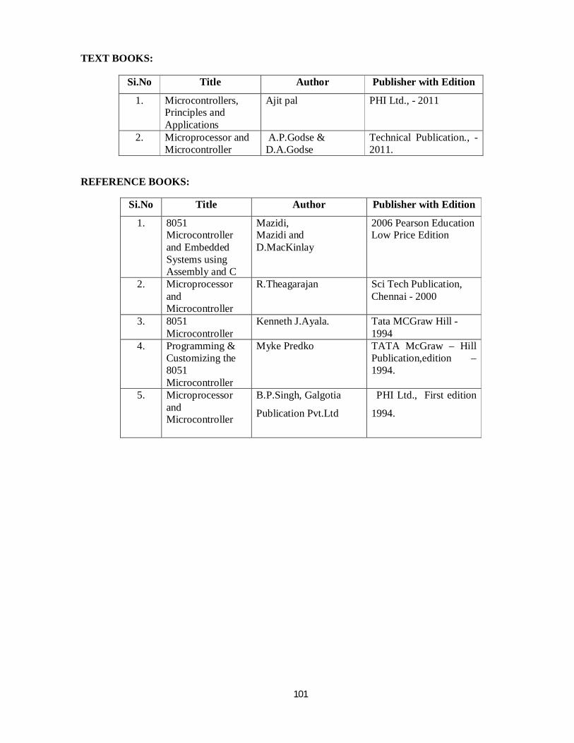
TEXT BOOKS:
Si.No Title Author Publisher with Edition
1. Microcontrollers, Principles and Applications
Ajit pal PHI Ltd., - 2011
2. Microprocessor and Microcontroller
A.P.Godse & D.A.Godse
Technical Publication., - 2011.
REFERENCE BOOKS: Si.No Title Author Publisher with Edition
1. 8051 Microcontroller and Embedded Systems using Assembly and C
Mazidi, Mazidi and D.MacKinlay
2006 Pearson Education Low Price Edition
2. Microprocessor and Microcontroller
R.Theagarajan Sci Tech Publication, Chennai - 2000
3. 8051 Microcontroller
Kenneth J.Ayala.
Tata MCGraw Hill - 1994
4. Programming & Customizing the 8051 Microcontroller
Myke Predko TATA McGraw – Hill Publication,edition – 1994.
5. Microprocessor and Microcontroller
B.P.Singh, Galgotia
Publication Pvt.Ltd
PHI Ltd., First edition
1994.
102
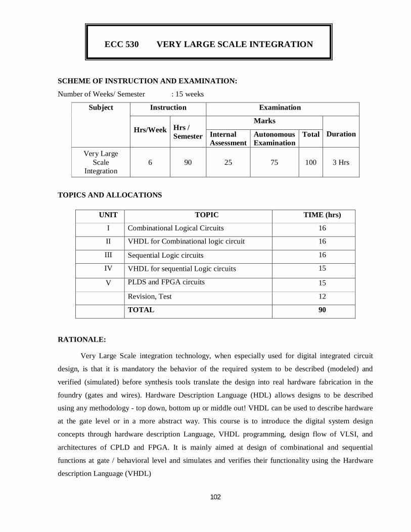
SCHEME OF INSTRUCTION AND EXAMINATION:
Number of Weeks/ Semester : 15 weeks
Subject Instruction Examination
Hrs/Week Hrs / Semester
Marks
Duration Internal Assessment
Autonomous Examination
Total
Very Large Scale
Integration
6
90 25 75 100 3 Hrs
TOPICS AND ALLOCATIONS
UNIT TOPIC TIME (hrs)
I Combinational Logical Circuits 16
II VHDL for Combinational logic circuit 16
III Sequential Logic circuits 16
IV VHDL for sequential Logic circuits 15
V PLDS and FPGA circuits 15
Revision, Test 12
TOTAL 90
RATIONALE:
Very Large Scale integration technology, when especially used for digital integrated circuit
design, is that it is mandatory the behavior of the required system to be described (modeled) and
verified (simulated) before synthesis tools translate the design into real hardware fabrication in the
foundry (gates and wires). Hardware Description Language (HDL) allows designs to be described
using any methodology - top down, bottom up or middle out! VHDL can be used to describe hardware
at the gate level or in a more abstract way. This course is to introduce the digital system design
concepts through hardware description Language, VHDL programming, design flow of VLSI, and
architectures of CPLD and FPGA. It is mainly aimed at design of combinational and sequential
functions at gate / behavioral level and simulates and verifies their functionality using the Hardware
description Language (VHDL)
ECC 530 VERY LARGE SCALE INTEGRATION
103
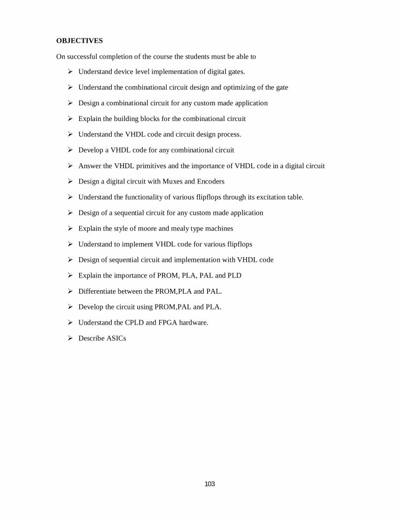
OBJECTIVES
On successful completion of the course the students must be able to
Understand device level implementation of digital gates.
Understand the combinational circuit design and optimizing of the gate
Design a combinational circuit for any custom made application
Explain the building blocks for the combinational circuit
Understand the VHDL code and circuit design process.
Develop a VHDL code for any combinational circuit
Answer the VHDL primitives and the importance of VHDL code in a digital circuit
Design a digital circuit with Muxes and Encoders
Understand the functionality of various flipflops through its excitation table.
Design of a sequential circuit for any custom made application
Explain the style of moore and mealy type machines
Understand to implement VHDL code for various flipflops
Design of sequential circuit and implementation with VHDL code
Explain the importance of PROM, PLA, PAL and PLD
Differentiate between the PROM,PLA and PAL.
Develop the circuit using PROM,PAL and PLA.
Understand the CPLD and FPGA hardware.
Describe ASICs
104
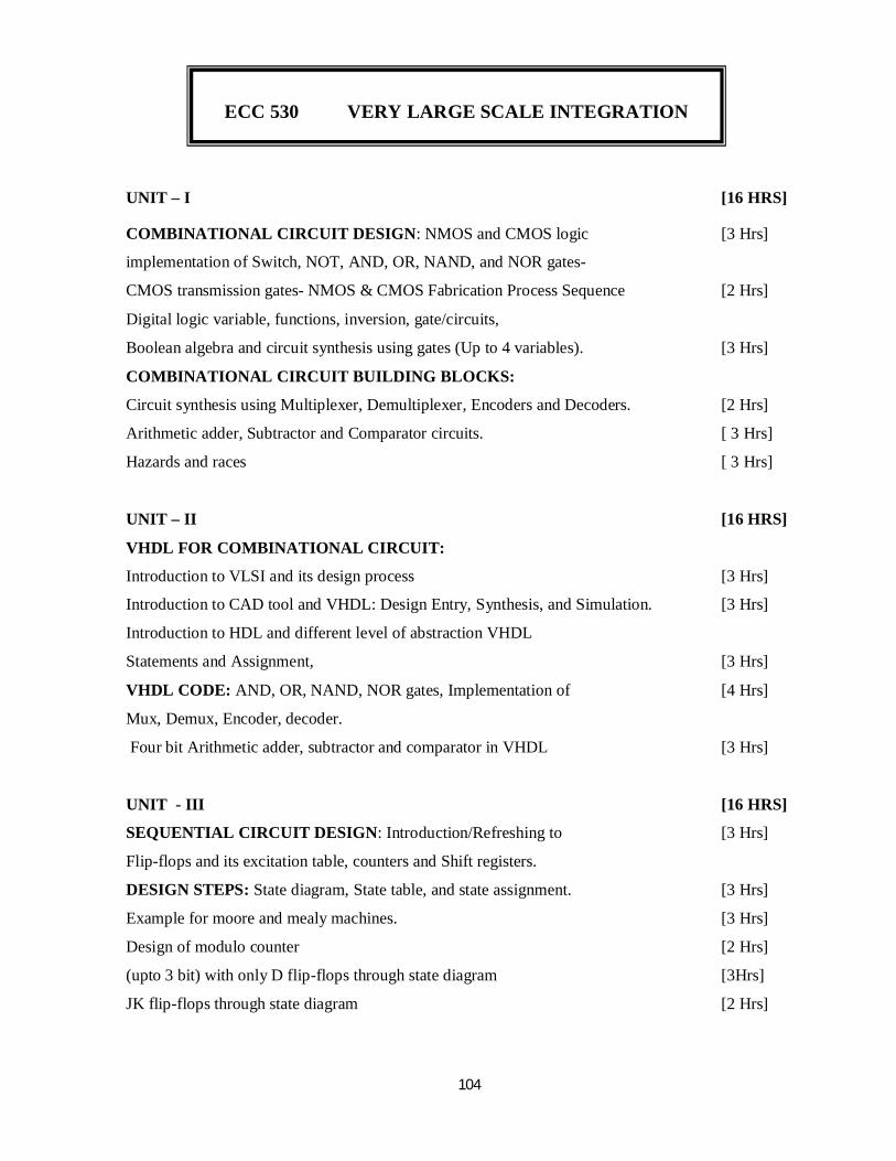
UNIT – I [16 HRS]
COMBINATIONAL CIRCUIT DESIGN: NMOS and CMOS logic [3 Hrs]
implementation of Switch, NOT, AND, OR, NAND, and NOR gates-
CMOS transmission gates- NMOS & CMOS Fabrication Process Sequence [2 Hrs]
Digital logic variable, functions, inversion, gate/circuits,
Boolean algebra and circuit synthesis using gates (Up to 4 variables). [3 Hrs]
COMBINATIONAL CIRCUIT BUILDING BLOCKS:
Circuit synthesis using Multiplexer, Demultiplexer, Encoders and Decoders. [2 Hrs]
Arithmetic adder, Subtractor and Comparator circuits. [ 3 Hrs]
Hazards and races [ 3 Hrs]
UNIT – II [16 HRS]
VHDL FOR COMBINATIONAL CIRCUIT:
Introduction to VLSI and its design process [3 Hrs]
Introduction to CAD tool and VHDL: Design Entry, Synthesis, and Simulation. [3 Hrs]
Introduction to HDL and different level of abstraction VHDL
Statements and Assignment, [3 Hrs]
VHDL CODE: AND, OR, NAND, NOR gates, Implementation of [4 Hrs]
Mux, Demux, Encoder, decoder.
Four bit Arithmetic adder, subtractor and comparator in VHDL [3 Hrs]
UNIT - III [16 HRS]
SEQUENTIAL CIRCUIT DESIGN: Introduction/Refreshing to [3 Hrs]
Flip-flops and its excitation table, counters and Shift registers.
DESIGN STEPS: State diagram, State table, and state assignment. [3 Hrs]
Example for moore and mealy machines. [3 Hrs]
Design of modulo counter [2 Hrs]
(upto 3 bit) with only D flip-flops through state diagram [3Hrs]
JK flip-flops through state diagram [2 Hrs]
ECC 530 VERY LARGE SCALE INTEGRATION
105
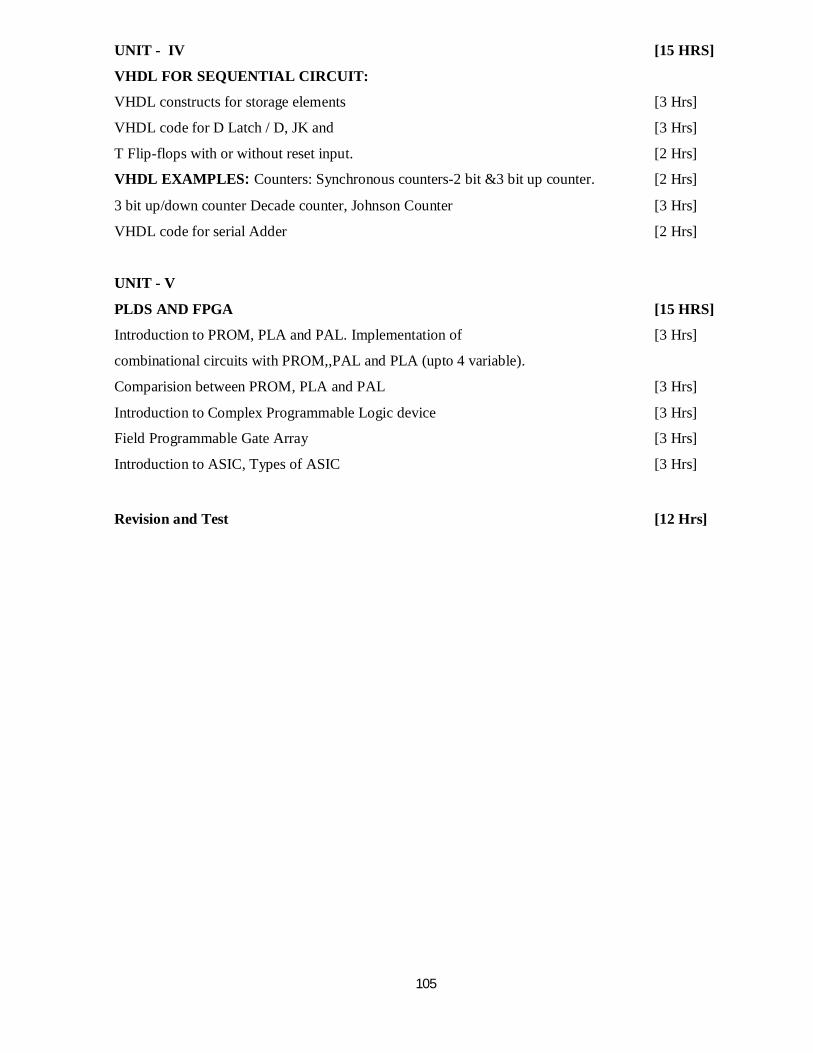
UNIT - IV [15 HRS]
VHDL FOR SEQUENTIAL CIRCUIT:
VHDL constructs for storage elements [3 Hrs]
VHDL code for D Latch / D, JK and [3 Hrs]
T Flip-flops with or without reset input. [2 Hrs]
VHDL EXAMPLES: Counters: Synchronous counters-2 bit &3 bit up counter. [2 Hrs]
3 bit up/down counter Decade counter, Johnson Counter [3 Hrs]
VHDL code for serial Adder [2 Hrs]
UNIT - V
PLDS AND FPGA [15 HRS]
Introduction to PROM, PLA and PAL. Implementation of [3 Hrs]
combinational circuits with PROM,,PAL and PLA (upto 4 variable).
Comparision between PROM, PLA and PAL [3 Hrs]
Introduction to Complex Programmable Logic device [3 Hrs]
Field Programmable Gate Array [3 Hrs]
Introduction to ASIC, Types of ASIC [3 Hrs]
Revision and Test [12 Hrs]
106
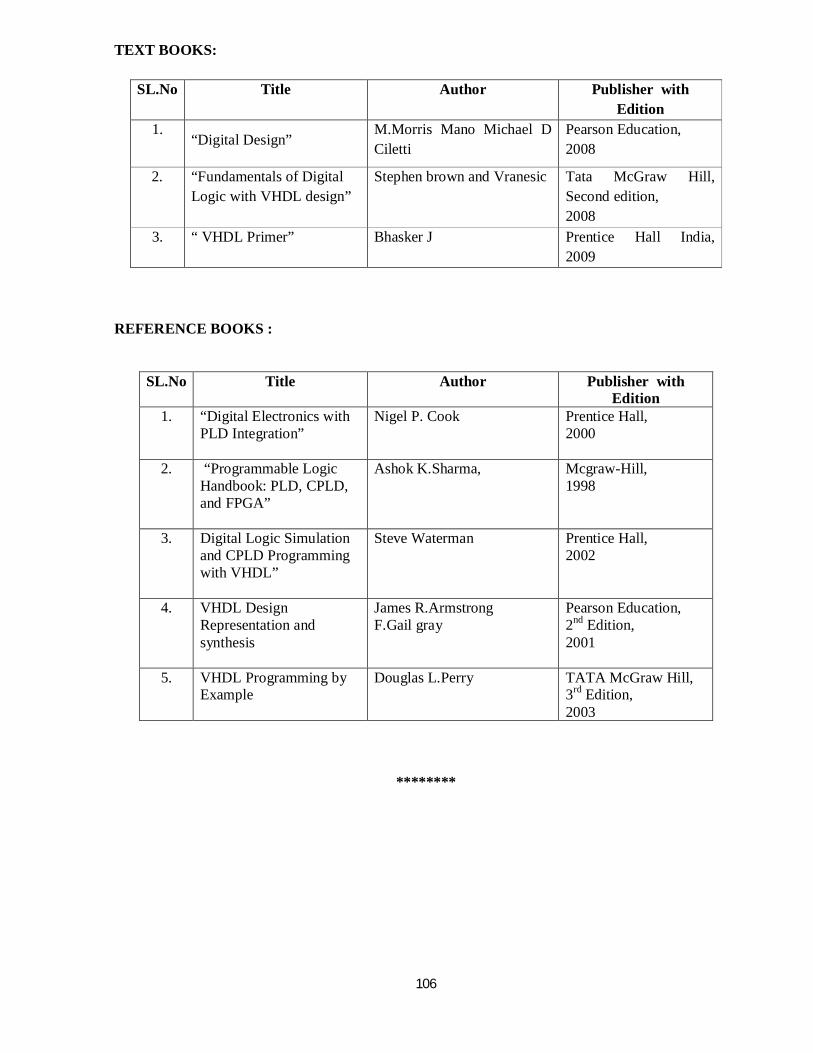
TEXT BOOKS:
SL.No Title Author Publisher with Edition
1. “Digital Design”
M.Morris Mano Michael D Ciletti
Pearson Education, 2008
2. “Fundamentals of Digital Logic with VHDL design”
Stephen brown and Vranesic Tata McGraw Hill, Second edition, 2008
3. “ VHDL Primer” Bhasker J Prentice Hall India, 2009
REFERENCE BOOKS :
SL.No Title Author Publisher with Edition
1. “Digital Electronics with PLD Integration”
Nigel P. Cook Prentice Hall, 2000
2. “Programmable Logic Handbook: PLD, CPLD, and FPGA”
Ashok K.Sharma, Mcgraw-Hill, 1998
3. Digital Logic Simulation and CPLD Programming with VHDL”
Steve Waterman Prentice Hall, 2002
4. VHDL Design Representation and synthesis
James R.Armstrong F.Gail gray
Pearson Education, 2nd Edition, 2001
5. VHDL Programming by Example
Douglas L.Perry TATA McGraw Hill, 3rd Edition, 2003
********
107
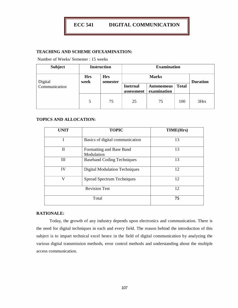
TEACHING AND SCHEME OFEXAMINATION:
Number of Weeks/ Semester : 15 weeks
Subject Instruction Examination
Digital Communication
Hrs week
Hrs semester
Marks Duration
Inetrnal assessment
Autonomous examination
Total
5
75
25
75
100
3Hrs
TOPICS AND ALLOCATION:
UNIT TOPIC TIME(Hrs)
I Basics of digital communication 13
II Formatting and Base Band Modulation
13
III Baseband Coding Techniques 13
IV Digital Modulation Techniques 12
V Spread Spectrum Techniques 12
Revision Test 12
Total 75
RATIONALE:
Today, the growth of any industry depends upon electronics and communication. There is
the need for digital techniques in each and every field. The reason behind the introduction of this
subject is to impart technical excel hence in the field of digital communication by analyzing the
various digital transmission methods, error control methods and understanding about the multiple
access communication.
ECC 541 DIGITAL COMMUNICATION
108
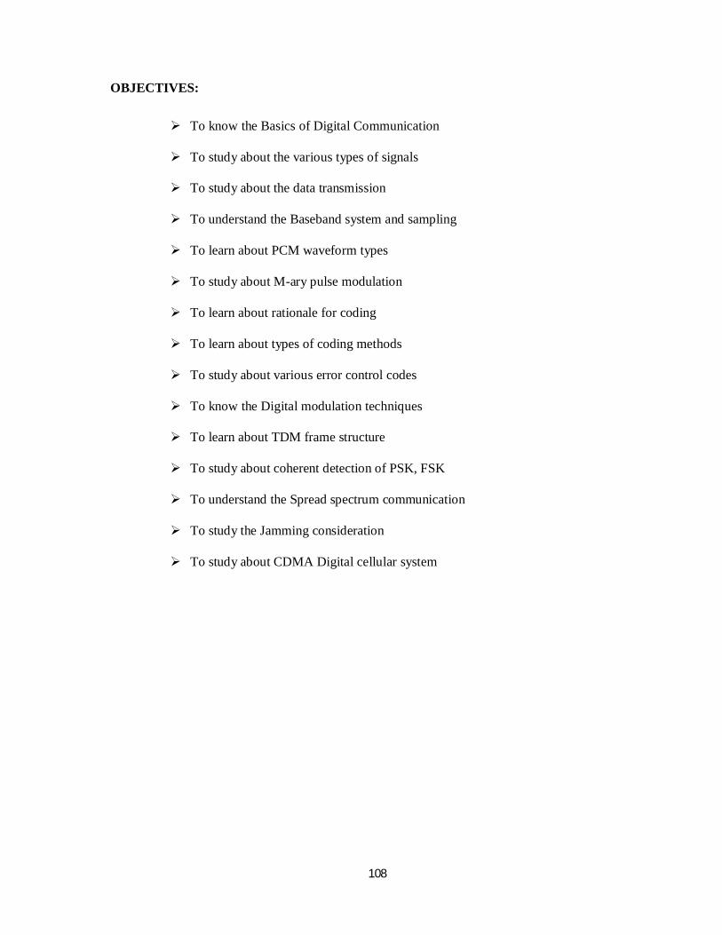
OBJECTIVES:
To know the Basics of Digital Communication
To study about the various types of signals
To study about the data transmission
To understand the Baseband system and sampling
To learn about PCM waveform types
To study about M-ary pulse modulation
To learn about rationale for coding
To learn about types of coding methods
To study about various error control codes
To know the Digital modulation techniques
To learn about TDM frame structure
To study about coherent detection of PSK, FSK
To understand the Spread spectrum communication
To study the Jamming consideration
To study about CDMA Digital cellular system
109
UNIT I
BASICS OF DIGITAL COMMUNICATION [13 Hrs]
Digital communication signal Processing – Typical Block diagram [2 Hrs]
of transformations
Advantages over analog communication – Channels for Digital communication [2 Hrs]
Telephone, Optical fiber, Satellite [2 Hrs]
Classification of signals – deterministic and random signals – Periodic and [2 Hrs]
non periodic signals – analog and discrete signals – energy and power signals –
unit impulse function
Information capacity (Definition only ) – Shannon’s limit for [2 Hrs]
information capacity (Definition only )
Data transmission [1 Hr]
Serial and parallel transmission -Synchronous and asynchronous transmission [2 Hrs]
UNIT II
FORMATTING AND BASEBAND MODULATION [13 Hrs]
Base band system – The Sampling theorem – impulse sampling – [2 Hrs]
natural sampling - Sample and hold operation – spectra [1 Hr]
Nyquist theorem – aliasing – signal interface for a digital system – Sampling [2 Hrs]
and quantizing effects- Quantization noise
channel effects – channel noise - PCM – uniform and Non-uniform quantization [2 Hrs]
Baseband Transmission:
PCM waveform types – non return-to-zero(NRZ) - return-to-zero(RZ) [2 Hrs]
Phase encoded – multilevel binary – special attributes of PCM waveforms [2 Hrs]
Bits per PCM word and Bits per symbol – PCM per size [2 Hrs]
M-ary pulse modulation Waveforms
ECC 541 DIGITAL COMMUNICATION
110
UNIT III
BASEBAND CODING TECHNIQUES: [13 Hrs]
Rationale for coding – Types of codes – Discrete memoryless channel [2 Hrs] Error control coding methods - Forward error correction [2 Hrs] Error detection with retransmission – types of error [2 Hrs] Random error and burst error [2 Hrs] Principles of linear block codes – Hamming code [3 Hrs] Binary cyclic codes - Cyclic redundancy check code(CRC) [2 Hrs] Convolution code
UNIT IV
DIGITAL MODULATION TECHNIQUES: [12 Hrs]
Digital modulation techniques – Listing of various types [2 Hrs]
Coherent binary modulation techniques - Coherent quadrature modulation
techniques – Non-Coherent binary modulation techniques [3 Hrs]
Minimum shift keying (MSK) – Block diagram of MSK transmitter and receiver [2 Hrs]
TDM – Frame structure, ASCII Framing
E1 Framing – T1 framing for telephone [2 Hrs]
Detection of signals – coherent detection of PSK – sampled matched filter
Coherent detection of FSK – Non-coherent detection – Binary differential PSK [3 Hrs]
UNIT V
SPREAD SPECTRUM TECHNIQUES : [12 Hrs]
Spread spectrum Communication – Beneficial attributes of Spread [3 Hrs]
spectrum systems - Pseudo noise sequences
Randomness properties – Balance property, Run property and [2 Hrs]
correlation property
Direct sequence spread spectrum systems – Processing gain and performance [2 Hrs]
Frequency hopping systems – Frequency hopping with diversity [2 Hrs]
Fast hopping versus – slow hopping – Synchronization – Jamming consideration [2 Hrs]
Commercial application – CDMA digital cellular system [1 Hr]
Revision and Test [12 Hrs]

111
TEXT BOOKS:
Sl. No
Title Author Publisher with Edition
1. Digital Communication Simon Haykins Wiley India edition, 2006
2. Principles of Digital communication
J.S.Chitode Tech Publications, Pune, Second edition,2011
REFERENCE BOOKS:
Sl.No Title Author Publisher with Edition 1. Digital communications
Fundamentals & Applications Bernard Sklar & Pabitra Kumar Ray
Pearson, Second edition, 2009
2. Digital and analog communication system
B.P.Lathi .Zhi Ding
OXFORD university press. International 4th Edition - 2001
3. Digital Communication P.Ramakrishna Rao
TMH, 2011
4. Principles of Communications system
Taub &Schilling
TMH, Third edition, 2008
5. Digital communications John G.Prokais
TMH 2011
6. Digital communications Dr.K.N.Hari Bhat Dr.D.Ganesh Rao
Sanguine Technical Publisher 2005
112
TEACHING AND SCHEME OFEXAMINATION:
Number of weeks per Semester: 15 weeks
Subject Instruction Examination
Programmable Logic Controllers
Hrs/ week
Hrs/ semester
Marks Duration
Inetrnal assessment
Autonomous examination
Total
5
75
25
75
100
3Hrs
TOPICS AND ALLOCATION:
UNIT TOPIC TIME(Hrs)
I Architecture and operation of PLC 13
II Programming of PLC 13
III PLC Timers and counters 13
IV Advanced instructions 12
V I/O Module Communication and
networking
12
Revision and Test 12
Total 75
RATIONALE
Programmable Logic Controller is the mandatory for the control Engineers in any Process Industry.
As it is the default controller being used in the industries in automation of process such as packing,
discrete control etc., It is obvious for the instrumentation and control Engineer to understand
Hardware and programming the PLC.
ECC 542 PROGRAMMABLE LOGIC CONTROLLERS
113
Objectives
To understand the detailed Hardware of PLC and its parts
To understand the working of PLC and scan cycle
T o understand the program and data memory organization
To know the Different timers of PLC and programming them
To know the different counters of PLC and its parameters
To understand the Ladder logic programming of PLC
To develop simple ladder programs
To study the Advanced instructions of PLC
To understand the communication module of PLC
114
UNIT I
ARCHITECTURE AND OPERATION OF PLC [13 HRS] Evolution of PLCs – Hard – Wired control systems [2 Hrs]
PLC definition, Features, Advantages, Relays
PLC parts and architecture – CPU - I/O section – Programming device [1 Hr]
Memory - input field devices –output field devices – input module wiring [2 Hrs]
connections, output module wiring connections
Power supply – PLC versus computer – Types of PLC [2 Hrs]
Single ended – Multitask – Control management – unitary [2 Hrs]
Modular – small – medium – large
Developing circuits from Boolean expressions – [2 Hrs]
Hardwired logic to programmed logic
Programming word level logic instruction – Processor memory organization [2 Hrs]
program files – Data files – Program Scan
UNIT II
PROGRAMMING OF PLC [13 Hrs]
PLC programming languages – Standard languages – Ladder diagram(LD) [2 Hrs]
Function block diagram(FBD) – Sequential function chart(SFC) [2 Hrs]
Statement list(STL) (each one example program)
Symbols of a PLC input and output contact graphical languages(IES) – [2 Hrs]
program format – Typical numbering mode
Equivalent ladder diagram of AND,OR,NOT,XOR,NAND and NOR [3 Hrs]
gate equivalent ladder diagram to demonstrates De-morgan’s theorem
Ladder design switches – Develop elementary [2 Hrs]
Program design of a 4:1 multiplexer using ladder logic programming [2 Hrs]
wired level logic instructions input, output, flag, timer, counter, latch
ECC 542 PROGRAMMABLE LOGIC CONTROLLERS
115
UNIT III
PLC TIMERS AND COUNTERS [13 HRS]
Definition and classification of a timer – Characteristics of a PLC timer [2 Hrs]
Functions in a timer - resetting – retentive functions and function block format – non retentive [3 Hrs] Classification – Timer ON–delay – timer – OFF delay Simple problems using timer [2 Hrs] PLC counter – Operation of a PLC counter – Counter parameters [2 Hrs] Format of counter instruction and counter data file [2 Hrs] count up (CTU) – count down (CTD) simple Problems using counter. [2 Hrs]
UNIT IV
ADVANCED INSTRUCTION [12 HRS]
Introduction – Comparison instructions – Addressing format [2 Hrs] for micro logic system Different addressing types – Data movement instructions - [2 Hrs] mathematical instructions Program flow control instructions – PID instructions [1 Hr] Program development and execution using Allen bradly PLC. [2 Hrs] Simplified start up process of a coal feeding of a boiler plant [2 Hrs] Elevator for 3 floor building – Traffic light control – Conveyor belt [2 Hrs] Selection of PLC – Safety consideration built in the PLC’s. [1 Hr]
UNIT V
I/O MODULE COMMUNICATION AND NETWORKING [12 HRS]
Introduction – Classification of I/O module input – output system [2 Hrs] Direct I/O,Parallel I/O – Sourcing and sinking of serial I/O system. PLC interfacing – Discrete input module – DC – AC – Discrete [2 Hrs] output module - analog input module single ended and output module [2 Hrs] RTD input module - Thermocouple – High speed encoder Stepper motor – RS-232 interface module Differential input module – Types of communication interface [1 Hr] Parallel – Serial – IEEE 488 bus – serial balanced – unbalanced Communication mode - Simplex – Half duplex [2 Hrs] Full duplex features of good interface [1 Hr] Serial interface RS232c. DB-9 connection of RS232
Network topology, Bus, ring, Star, Tree [2 Hrs]
Revision and Test [12 Hrs]
116
TEXT BOOKS:
REFERENCE BOOKS:
S.No Title Author Publisher with Edition 1. Programmable Logic
Controllers; Principles and applications
Jhon W Webb Ronald A Rels
PHI Learning Pvt. Ltd. 2012
2. Exploring Programmable Logic Controllers with Applications
Srivastava
BPB Publishers, 2012
3. Programmable Logic Controller
Vijay R Yadhav
Khanna Publishers, 2010
4. Programmable Logic Controllers
Gray Dunning Tata MC Graw Hill, 2009
S.No Title Author Publisher with Edition 1. Introduction to
Programmable Logic Controller
Gary Dunning Thomson Delmar learning, Second Edition, 2008
2. Programmable Logic Controller
FrankD.Petruzella Tata MC Graw Hill, Third Edition, 2010
117
TEACHING AND SCHEME OFEXAMINATION:
Number of weeks per Semester: 15 weeks
Subject Instruction Examination
Bio Medical Instrumentation
Hrs/ week
Hrs/ semester
Marks Duration
Inetrnal assessment
Autonomous examination
Total
5 75 25 75 100 3Hrs
TOPICS AND ALLOCATION:
UNIT TOPIC TIME(Hrs) I Bio - electric signals, electrodes and
clinical measurement
13
II Bio - medical recorders
13
III Therapeutic instruments
13
IV Biotelemetry and patient safety
12
V Modern imaging techniques
12
Revision and Test 12
Total 75
RATIONALE Bio medical engineering education is in the growing stage. But every year, there is a tremendous
increase in the use of modern medical equipment in the hospital and health care industry therefore it
is necessary for every student to understand the functioning of various medical equipments. This
subject to enable the students to learn the basic principles of different biomedical instruments viz
Clinical measurement, Bio - medical recorders, Therapeutic instruments, Biotelemetry and Modern
imaging techniques instruments.
ECC 550 BIO MEDICAL INSTRUMENTATION
118
OBJECTIVES
After learning this subject the student will be able to understand the about The generation of Bio-potential and its measurement using various electrodes.
The measurement of blood pressure.
The measurement of lung volume.
The measurement of respiration rate.
The measurement of body temperature and skin temperature.
The principles of operations of ECG recorder.
The principles of operations of EEG recorder.
The principles of operations of ENG recorder.
The working principles of audio meter.
The principles of operations of pacemaker.
The basic principle of dialysis.
The basic principle of short wave diathermy.
The basic principle of ventilators.
The working principles of telemetry.
The basic principle of telemedicine.
To learn about patient safety.
The various methods of accident prevention.
The basic principle of various types of lasers. The basic principle of CT and MRI scanner.
The principle of operation of various imaging techniques
119
UNIT-I
BIO-ELECTRIC SIGNALS AND ELECTRODES [13 Hrs]
Elementary ideas of cell structure, Bio – potential and their generation [2 Hrs]
resting and action potential – propagation of action potential. [2 Hrs]
Electrodes – Micro – Skin surface – needle electrodes. [2 Hrs]
CLINICAL MEASUREMENT:
Measurement of Blood pressure (direct, indirect) [2 Hrs]
blood flow meter (Electro magnetic& ultrasonic blood flow meter)
blood pH measurement - Measurement of Respiration rate [2 Hrs]
measurement of lung volume – heart rate measurement
Measurement of body and skin temperature – [2 Hrs]
Chromatography, Photometry, Flurometry. [1 Hr]
UNIT-II [13 Hrs]
BIO - MEDICAL RECORDERS:
Electro cardiograph (ECG) – Lead system – ECG electrodes – [2 Hrs]
ECG amplifiers – ECG recording units – analysis of ECG curves. [2 Hrs]
Nervous system – EEG recorder – 10-20 lead system – recording techniques – [2 Hrs]
EEG wave types – Clinical use of EEG – brain tumour Electro – [2 Hrs]
myograph (EMG) – EMG waves – measurement of conduction velocity – [1 Hrs]
EMG recording techniques – [2 Hrs]
Electro – retinograph (ERG) Audiometer – principle – types –
Basics audiometer working. [2 Hrs]
UNIT-III
THERAPEUTIC INSTRUMENTS: [13 Hrs]
Cardiac pacemaker – classification – External pace makers – [2 Hrs]
implantable pacemaker – pacing techniques – programmable pacemaker [2 Hrs]
Cardiac defibrillators – types – AC and DC defibrillators – [2 Hrs]
Heart lung machine with Block diagram. Dialysis – [2 Hrs]
ECC 550 BIO MEDICAL INSTRUMENTATION
120
Hemo dialysis – peritoneal dialysis.
Endoscopes Endoscopic laser coagulator and applications [2 Hrs]
physiotherapy equipment – short wave diathermy
micro wave diathermy – ultrasonic therapy unit (block / circuit) [2 Hrs]
Ventilators – types – modern ventilator block diagram. [1 Hr]
UNIT-IV
BIOTELEMETRY AND PATIENT SAFETY [12 Hrs]
Introduction to biotelemetry – physiological – adaptable to biotelemetry [2 Hrs]
components of a biotelemetry system – application of telemetry
elements of biotelemetry; AM, FM transmitter and receiver
requirements for biotelemetry system – radio telemetry with sub carrier [2 Hrs]
single channel and multi channel telemetry
Telemedicine; introduction, working, applications.
Patient safety: Physiological effects of electric current – Micro and macro shock [2 Hrs]
leakage current – shock hazards from electrical equipment.
Methods of Accident Prevention – Grounding – Double Insulation [2 Hrs]
Protection by low voltage – Ground fault circuit interrupter
Isolation of patient connected parts – Isolated power distribution system. [2 Hrs]
Safety aspects in electro surgical units [1 Hr]
burns, high frequency current hazards, Explosion hazards. [1 Hr]
UNIT-V [12 Hrs]
MODERN IMAGING TECHNIQUES:
LASER beam properties – block diagram – operation of CO2 and NDYag LASER [2 Hrs]
applications of LASER in medicine. X ray apparatus – block diagram – operation [3 Hrs]
special techniques in X-ray imaging – Tomogram – computerized Axial tomography [3 Hrs]
Ultrasonic imaging techniques – Echo cardiography – Angiography [2 Hrs]
CT scanner - Magnetic resonance imaging techniques. [2 Hrs]
Revision and Test [12 Hrs]
121
TEXT BOOKS:
Si.No Title Author Publisher with Edition
1. Biomedical Instrumentation Dr.M. Arumugam Anuradha publications, chennai edition, 2003
REFERENCE BOOKS:
S.No Title Author Publisher with Edition
1. Biomedical Instrumentation and measurement
Leslie Cromwell – Fred.J.
Weibell, ErichA.P Feither
IIedition,Pearson
education,2008
2. Medicine and clinical Engineering
Jacobson and Webstar
PHI publishers, 2010
3. Hand book of Bio –Medical Instrumentation .
R.S .Khandpur
CBS publications, 1st
edition ,2007
4. Medical Electronics Kumara doss
Tata mcgraw hill, 2nd
edition, 2003
5. Introduction to Medical Electronics
B.R. Klin
IV edition, pearson
education, 2008
6. Introduction to Biomedical Instrumentation
Mandeep Singh
Printice Hall India 2010.
122
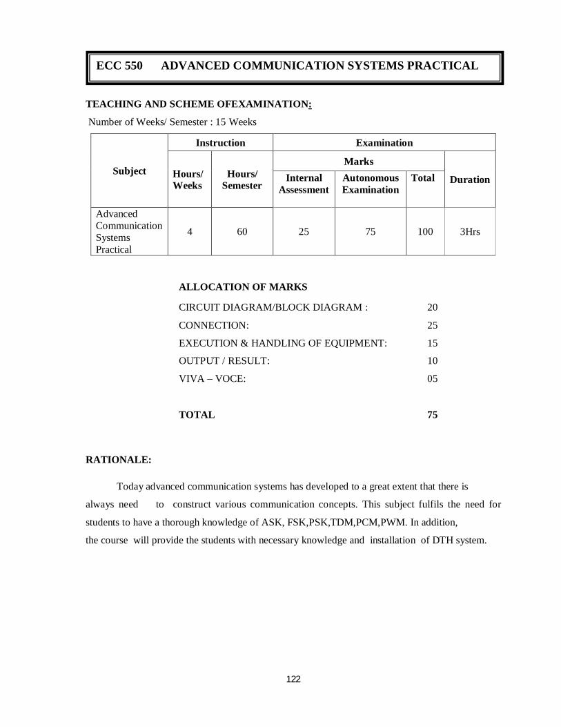
TEACHING AND SCHEME OFEXAMINATION:
Number of Weeks/ Semester : 15 Weeks
Subject
Instruction Examination
Hours/ Weeks
Hours/ Semester
Marks
Duration Internal Assessment
Autonomous Examination
Total
Advanced Communication Systems Practical
4 60 25 75 100 3Hrs
ALLOCATION OF MARKS
CIRCUIT DIAGRAM/BLOCK DIAGRAM : 20
CONNECTION: 25
EXECUTION & HANDLING OF EQUIPMENT: 15
OUTPUT / RESULT: 10
VIVA – VOCE: 05
TOTAL 75
RATIONALE: Today advanced communication systems has developed to a great extent that there is
always need to construct various communication concepts. This subject fulfils the need for
students to have a thorough knowledge of ASK, FSK,PSK,TDM,PCM,PWM. In addition,
the course will provide the students with necessary knowledge and installation of DTH system.
ECC 550 ADVANCED COMMUNICATION SYSTEMS PRACTICAL
123
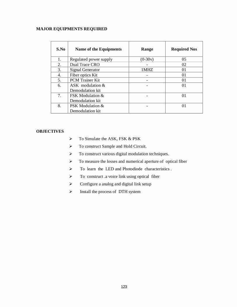
MAJOR EQUIPMENTS REQUIRED
S.No
Name of the Equipments
Range
Required Nos
1. Regulated power supply (0-30v) 05 2. Dual Trace CRO - 02 3. Signal Generator 1MHZ 01 4. Fiber optics Kit - 01 5. PCM Trainer Kit - 01 6. ASK modulation &
Demodulation kit - 01
7. FSK Modulation & Demodulation kit
- 01
8. PSK Modulation & Demodulation kit
- 01
OBJECTIVES
To Simulate the ASK, FSK & PSK
To construct Sample and Hold Circuit.
To construct various digital modulation techniques.
To measure the losses and numerical aperture of optical fiber
To learn the LED and Photodiode characteristics .
To construct .a voice link using optical fiber
Configure a analog and digital link setup
Install the process of DTH system
124
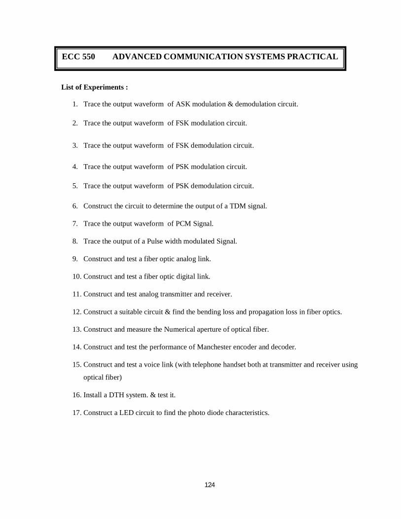
List of Experiments :
1. Trace the output waveform of ASK modulation & demodulation circuit.
2. Trace the output waveform of FSK modulation circuit.
3. Trace the output waveform of FSK demodulation circuit.
4. Trace the output waveform of PSK modulation circuit.
5. Trace the output waveform of PSK demodulation circuit.
6. Construct the circuit to determine the output of a TDM signal.
7. Trace the output waveform of PCM Signal.
8. Trace the output of a Pulse width modulated Signal.
9. Construct and test a fiber optic analog link.
10. Construct and test a fiber optic digital link.
11. Construct and test analog transmitter and receiver.
12. Construct a suitable circuit & find the bending loss and propagation loss in fiber optics.
13. Construct and measure the Numerical aperture of optical fiber.
14. Construct and test the performance of Manchester encoder and decoder.
15. Construct and test a voice link (with telephone handset both at transmitter and receiver using
optical fiber)
16. Install a DTH system. & test it.
17. Construct a LED circuit to find the photo diode characteristics.
ECC 550 ADVANCED COMMUNICATION SYSTEMS PRACTICAL
125
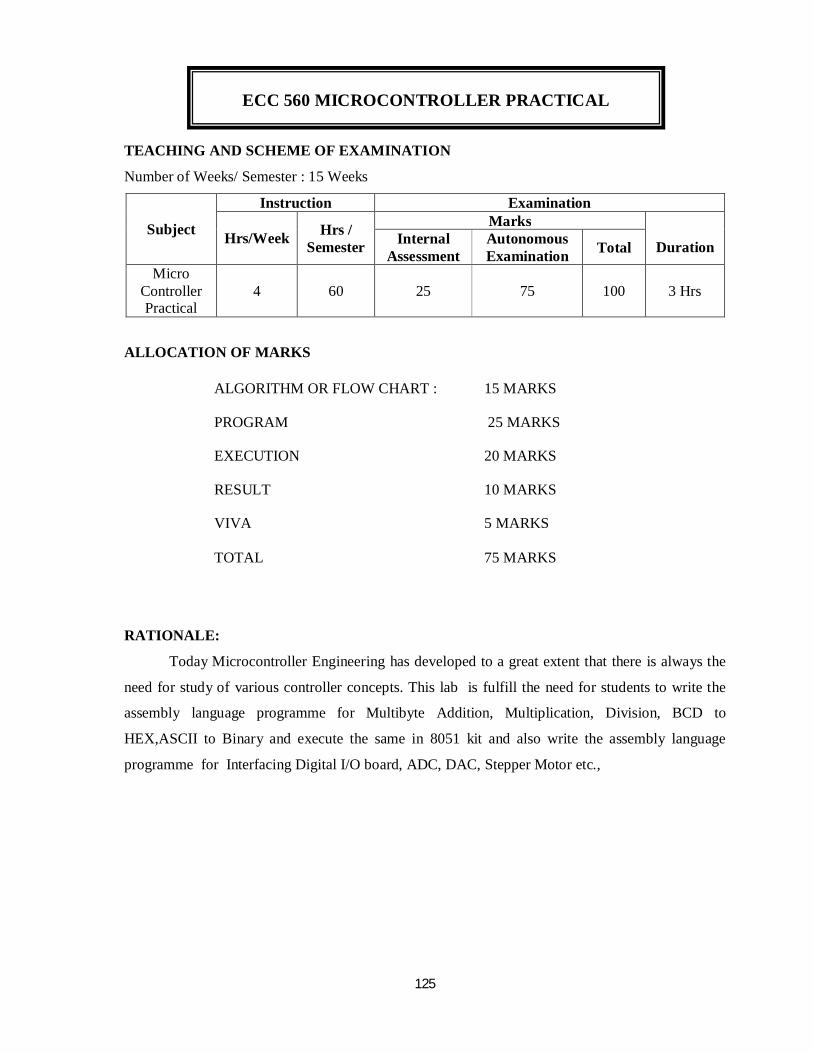
TEACHING AND SCHEME OF EXAMINATION
Number of Weeks/ Semester : 15 Weeks
Subject
Instruction Examination
Hrs/Week Hrs / Semester
Marks Duration Internal
Assessment Autonomous Examination Total
Micro Controller Practical
4 60 25 75 100 3 Hrs
ALLOCATION OF MARKS
ALGORITHM OR FLOW CHART : 15 MARKS
PROGRAM 25 MARKS
EXECUTION 20 MARKS
RESULT 10 MARKS
VIVA 5 MARKS TOTAL 75 MARKS
RATIONALE:
Today Microcontroller Engineering has developed to a great extent that there is always the
need for study of various controller concepts. This lab is fulfill the need for students to write the
assembly language programme for Multibyte Addition, Multiplication, Division, BCD to
HEX,ASCII to Binary and execute the same in 8051 kit and also write the assembly language
programme for Interfacing Digital I/O board, ADC, DAC, Stepper Motor etc.,
ECC 560 MICROCONTROLLER PRACTICAL
126
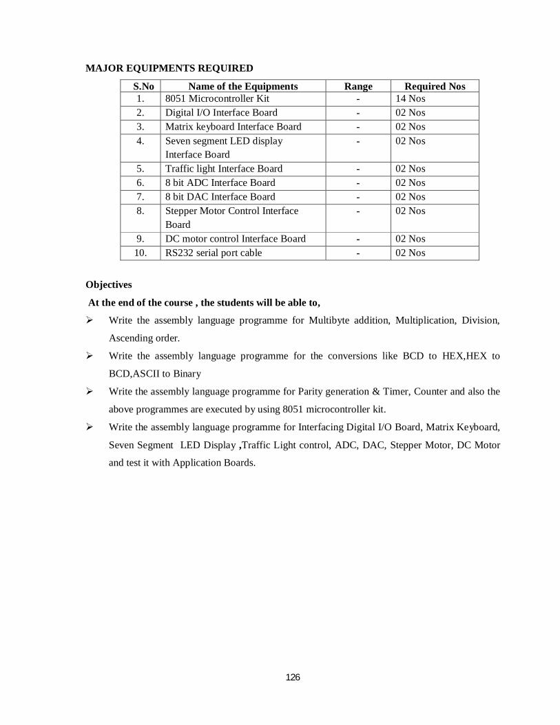
MAJOR EQUIPMENTS REQUIRED
S.No Name of the Equipments Range Required Nos 1. 8051 Microcontroller Kit - 14 Nos 2. Digital I/O Interface Board - 02 Nos 3. Matrix keyboard Interface Board - 02 Nos 4. Seven segment LED display
Interface Board - 02 Nos
5. Traffic light Interface Board - 02 Nos 6. 8 bit ADC Interface Board - 02 Nos 7. 8 bit DAC Interface Board - 02 Nos 8. Stepper Motor Control Interface
Board - 02 Nos
9. DC motor control Interface Board - 02 Nos 10. RS232 serial port cable - 02 Nos
Objectives
At the end of the course , the students will be able to,
Write the assembly language programme for Multibyte addition, Multiplication, Division,
Ascending order.
Write the assembly language programme for the conversions like BCD to HEX,HEX to
BCD,ASCII to Binary
Write the assembly language programme for Parity generation & Timer, Counter and also the
above programmes are executed by using 8051 microcontroller kit.
Write the assembly language programme for Interfacing Digital I/O Board, Matrix Keyboard,
Seven Segment LED Display ,Traffic Light control, ADC, DAC, Stepper Motor, DC Motor
and test it with Application Boards.
127
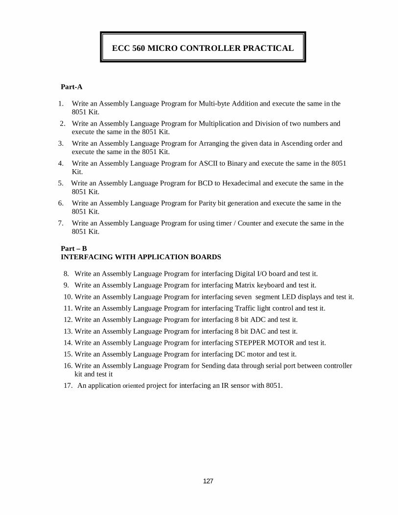
Part-A
1. Write an Assembly Language Program for Multi-byte Addition and execute the same in the 8051 Kit.
2. Write an Assembly Language Program for Multiplication and Division of two numbers and execute the same in the 8051 Kit.
3. Write an Assembly Language Program for Arranging the given data in Ascending order and execute the same in the 8051 Kit.
4. Write an Assembly Language Program for ASCII to Binary and execute the same in the 8051 Kit.
5. Write an Assembly Language Program for BCD to Hexadecimal and execute the same in the 8051 Kit.
6. Write an Assembly Language Program for Parity bit generation and execute the same in the 8051 Kit.
7. Write an Assembly Language Program for using timer / Counter and execute the same in the 8051 Kit.
Part – B INTERFACING WITH APPLICATION BOARDS 8. Write an Assembly Language Program for interfacing Digital I/O board and test it. 9. Write an Assembly Language Program for interfacing Matrix keyboard and test it. 10. Write an Assembly Language Program for interfacing seven segment LED displays and test it. 11. Write an Assembly Language Program for interfacing Traffic light control and test it. 12. Write an Assembly Language Program for interfacing 8 bit ADC and test it. 13. Write an Assembly Language Program for interfacing 8 bit DAC and test it. 14. Write an Assembly Language Program for interfacing STEPPER MOTOR and test it. 15. Write an Assembly Language Program for interfacing DC motor and test it. 16. Write an Assembly Language Program for Sending data through serial port between controller
kit and test it 17. An application oriented project for interfacing an IR sensor with 8051.
ECC 560 MICRO CONTROLLER PRACTICAL
128
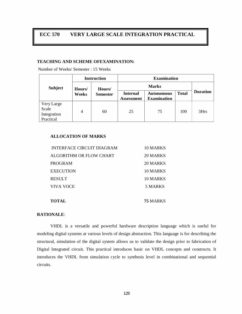
TEACHING AND SCHEME OFEXAMINATION:
Number of Weeks/ Semester : 15 Weeks
Subject
Instruction Examination
Hours/ Weeks
Hours/ Semester
Marks Duration Internal
Assessment Autonomous Examination
Total
Very Large Scale Integration Practical
4 60 25 75 100 3Hrs
ALLOCATION OF MARKS
INTERFACE CIRCUIT DIAGRAM 10 MARKS
ALGORITHM OR FLOW CHART 20 MARKS
PROGRAM 20 MARKS
EXECUTION 10 MARKS
RESULT 10 MARKS
VIVA VOCE 5 MARKS
TOTAL 75 MARKS
RATIONALE: VHDL is a versatile and powerful hardware description language which is useful for
modeling digital systems at various levels of design abstraction. This language is for describing the
structural, simulation of the digital system allows us to validate the design prior to fabrication of
Digital Integrated circuit. This practical introduces basic on VHDL concepts and constructs. It
introduces the VHDL from simulation cycle to synthesis level in combinational and sequential
circuits.
ECC 570 VERY LARGE SCALE INTEGRATION PRACTICAL

129
GUIDELINES:
All the experiments given in the list of experiments should be completed and given for the end
semester practical examination.
In order to develop best skills in handling Instruments/Equipment and taking readings in the
practical classes, every three students should be provided with a separate experimental setup
fordoing experiments in the laboratory.
The external examiners are requested to ensure that a single experimental question should not be
given to more than three students while admitting a batch of 30 students during Board
Examinations.
MAJOR EQUIPMENTS REQUIRED
S.No Name of the Equipments Range Required Nos 1. FPGA KIT with atleast 10
switches for input, 8 LEDs for output, a 7 segment display, debounced push switch ( 2 Nos) for manual clock input and external clock source.
- 10 Nos.
OBJECTIVES
On successful completion of the course the students must be able to
Simulation of VHDL code a combinational circuit
Simulation of VHDL code a for Arithmetic Circuits
Simulation of VHDL code a for Multiplexer.
Implementation of Multiplexer
Implementation of Demultiplexer
Implementation of Decoder
Implementation of Encoder
130
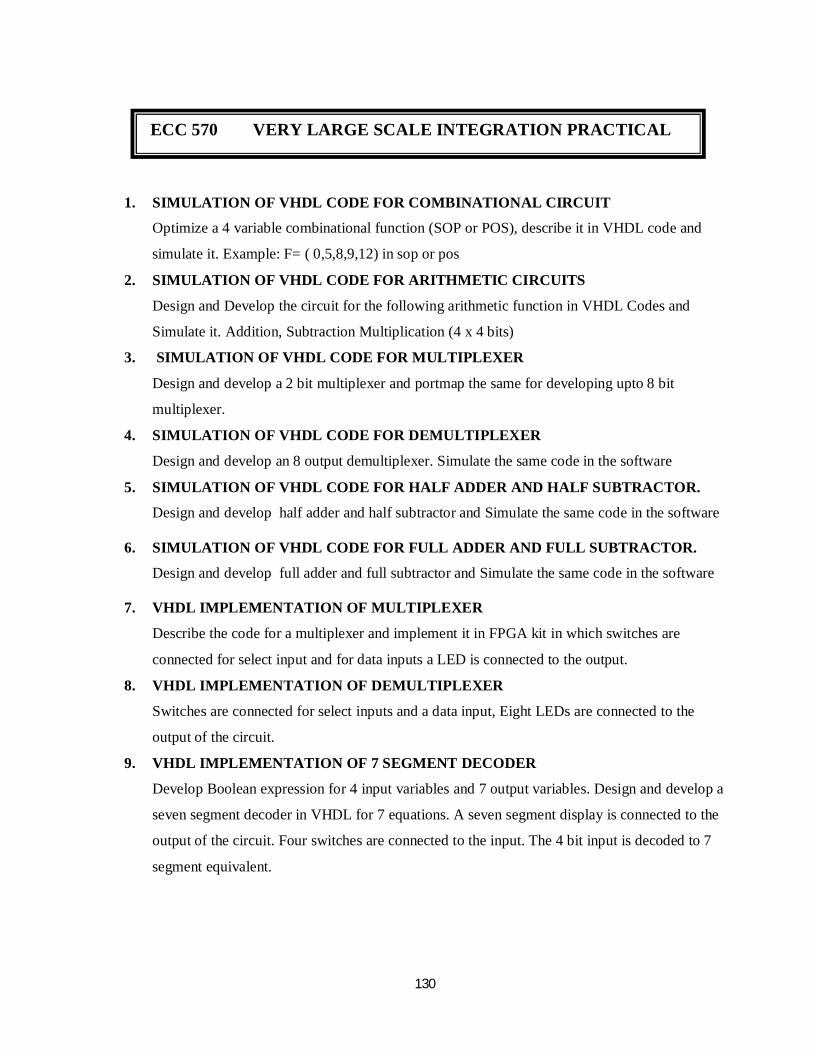
1. SIMULATION OF VHDL CODE FOR COMBINATIONAL CIRCUIT
Optimize a 4 variable combinational function (SOP or POS), describe it in VHDL code and
simulate it. Example: F= ( 0,5,8,9,12) in sop or pos
2. SIMULATION OF VHDL CODE FOR ARITHMETIC CIRCUITS
Design and Develop the circuit for the following arithmetic function in VHDL Codes and
Simulate it. Addition, Subtraction Multiplication (4 x 4 bits)
3. SIMULATION OF VHDL CODE FOR MULTIPLEXER
Design and develop a 2 bit multiplexer and portmap the same for developing upto 8 bit
multiplexer.
4. SIMULATION OF VHDL CODE FOR DEMULTIPLEXER
Design and develop an 8 output demultiplexer. Simulate the same code in the software
5. SIMULATION OF VHDL CODE FOR HALF ADDER AND HALF SUBTRACTOR.
Design and develop half adder and half subtractor and Simulate the same code in the software
6. SIMULATION OF VHDL CODE FOR FULL ADDER AND FULL SUBTRACTOR.
Design and develop full adder and full subtractor and Simulate the same code in the software
7. VHDL IMPLEMENTATION OF MULTIPLEXER
Describe the code for a multiplexer and implement it in FPGA kit in which switches are
connected for select input and for data inputs a LED is connected to the output.
8. VHDL IMPLEMENTATION OF DEMULTIPLEXER
Switches are connected for select inputs and a data input, Eight LEDs are connected to the
output of the circuit.
9. VHDL IMPLEMENTATION OF 7 SEGMENT DECODER
Develop Boolean expression for 4 input variables and 7 output variables. Design and develop a
seven segment decoder in VHDL for 7 equations. A seven segment display is connected to the
output of the circuit. Four switches are connected to the input. The 4 bit input is decoded to 7
segment equivalent.
ECC 570 VERY LARGE SCALE INTEGRATION PRACTICAL
131
10. VHDL IMPLEMENTATION OF 7 SEGMENT DECODER BY LUT
Develop a 7 segment decoder using Look up table. Describe the seven segment decoder in
VHDL using developed Look up table. A seven segment display is connected to the output of
the circuit. Four switches are connected to the input. The 4 bit input is decoded into 7 segment
equivalent.
11. VHDL IMPLEMENTATION OF ENCODER
Design and develop HDL code for decimal (Octal) to BCD encoder. There will be10 input
switches (or 8 switches) and 4 LEDs in the FPGA kit. The input given from switches and it is
noted that any one of the switch is active. The binary equivalent for the corresponding input
switch will be glowing in the LED as output.
12. SIMULATION OF VHDL CODE FOR DELAY
Develop a VHDL code for making a delayed output for 1second or 2 seconds by assuming
clock frequency provided in the FPGA Kit.
13. VHDL IMPLEMENTATION FOR BLINKING A LED
Develop a VHDL Code for delay and verify by simulating it. This delay output is connected to
LED. Delay is adjusted such away LED blinks for every 1 or 2 seconds.
14. SIMULATE A VHDL TEST BENCH CODE FOR TESTING A GATE
Develop a VHDL test bench code for testing any one of the simple gate. Simulate the test
bench code in the HDL software.
15. VHDL IMPLEMENTATION FOR BLINKING A ARRAY OF LEDS
Design and develop a VHDL Code for 4 bit binary up counter. Four LEDs are connected at the
output of the counter. The counter should up for every one seconds.
16. VHDL IMPLEMENTATION OF A SPELLER WITH AN ARRAY OF LEDS
Design and develop VHDL Code for a 5 bit Johnson ring counter 4 bit The LEDs are
connected at the output of the counter. The speller should work for every one seconds.
17. VHDL IMPLEMENTATION OF 7 SEGMENT DISPLAY
Design and develop a seven segment decoder in VHDL. Design and develop a 4 bit BCD
counter, the output of the counter is given to seven segment decoder. A seven segment display
is connected to the output of the decoder. The display shows 0,1, 2.. 9 for every one second
132
Time : 3 hrs Max marks : 75
PART-A (5x2=10Marks)
Answer any 5 Questions 1. What is RADAR ?
2. What is ISDN?
3. Give example for optical source
4. Define apogee.
5. What is roaming?
6. What is TDMA?
7. What is GSM?
8. Name different types of orbit
PART-B (5x3=15 Marks)
Answer any 5 Questions 9. What is duplexer?
10. Write down the equation for channel capacity?
11. What is graded index fiber?
12. What are the uses of facsimile communication system?
13. What is fiber splice?
14. Compare surface emitter and edge emitter LEDs.
15. Mention the disadvantages of passive satellite.
16. Explain the term hand off.
ECC 510 ADVANCED COMMUNICATION SYSTEMS
MODEL QUESTION PAPER
133
PART-C (5x10=50 Marks) Answer all Questions choosing either division (A) or division (B) of each question 17. A) With the Block Diagram Explain Pulsed Radar System?
(OR) B) Explain Electronics Switching System With the Block Diagram.
18. A) Draw the Block Diagram Of FSK Modulation And Explain Each Block.
(OR) B) Explain Forward Error Correcting Code and Hamming Code
19 A) Explain the Block Diagram of Optical Transmitter and Receiver. (OR)
B) Explain the Principle of light transmission in fibre using ray theory 20. A) Briefly Explain Kepler’s I, II and III Laws.
(OR) B) With the Block Diagram Explain Transmit –Receive Earth Station. 21. A) Explain the fundamental concepts of cellular telephone system.
(OR) B) Draw the architecture of GSM system and explain its operation.
134
Time : 3 hrs Max marks : 75
PART-A (5x2=10Marks) Answer any 5 Questions
1) What is microcontroller?
2) What are the addressing modes of 8051?
3) What is assembler?
4) What are the modes of programming of timer?
5) Mention Counter programming?
6) State the use of interrupts in 8051?
7) What is RS 232C?
8) What are the modes of 8255?
PART-B (5x3=15 Marks)
Answer any 5 Questions
9) Explain about program counter ?
10) Write program about the 8 bit Multiplication of 2 nos?
11) Explain ASCII to BINARY Conversion?
12) How can you perform Mode 2 Programming?
13) Mention the SFR registers used in timer operation?
14) What is the function of C/T bit in TMOD register?
15) Draw the RS232 connection to 8051?
16) Explain the Dc Motor interfacing using PWM?
ECC 520 MICROCONTROLLER
MODEL QUESTION PAPER
135
PART-C (5x10=50 Marks) Answer all Questions choosing either division (A) or division (B) of each question
17. A) Explain the Block diagram of 8051 Microcontroller? (or)
B) Explain the Classification of 8051 instructions?
18) A) Explain the different addressing modes of 8051. (or) B) Explain Multibyte addition with program 19) A) Explain Bit addresses for I/O & RAM
(or) B) Explain the programming of Timer
20) A) Explain about 8051 Serial communication Programming. (or)
B) Explain Interrupt priority in 8051.
21) A) Explain IC 8255 with Block diagram (or)
B)Explain about the Stepper motor interfacing with 8051.
136
Time : 3 Hrs Max marks : 75
PART-A (5x2=10Marks)
Answer any 5 Questions 1. What are universal gates?
2. Define encoder.
3. Expand VHDL.
4. Draw the circuit for half adder.
5. Define state table.
6. Define serial adder.
7. Define PLA.
8. Expand ASIC. PART-B (5x3=15 Marks)
Answer any 5 Questions 9. What do you meant by hazards in digital circuit?
10. Define multiplexer.
11. Distinguish between combinational circuits and sequential circuits.
12. Define Timing simulation.
13. What do you mean by SISO & PISO?
14. Write the excitation table for D Flipflop?
15. Define Moore type FSM.
16. Give two examples for custom chip.
ECC 530 VERY LARGE SCALE INTEGRATION
MODEL QUESTION PAPER
137
PART-C (5x10=50 Marks) Answer all Questions choosing either division (A) or division (B) of each question 17. A) Implement the function f = ∑(1, 2, 3,5, 7,10,13) with do not care 4 & 6 with minimal gates.
(OR) B) Draw the circuit of NMOS NAND, NOR, AND, OR. 18. A) Explain in detail about assignment statements.
(OR) B) i)Write a VHDL code four bit comparator. ii) Write a VHDL code four bit adder. 19. A) Design a modulo 8 bit counter using D flip flop. Use proper excitation table & state diagram.
(OR) B) Explain about the moore & mealy machine and give out the examples. 20. A) Write down the VHDL code for modulo 6 bit up/down counter.
(OR) B) Write down the VHDL code for serial adder. 21 A) Implement the function F= ∑ m (0,1,2,3,5) in PAL.
(OR) B) Explain about CPLD and FPGA in detail.

138
Time : 3 hrs Max marks : 75
PART-A (5x2=10Marks) Answer any 5 Questions
1) What is digital communication?
2) What is an echo compressor?
3) Define sampling?
4) What is burst error?
5) What is PCM?
6) What is E1 framing?
7) What is MSK?
8) What is spread spectrum communication? PART-B (5x3=15 Marks)
Answer any 5 Questions. 9) What are the functions performed during the process of ADC?
10) What is meant by aliasing?
11) Explain the forward error correction.
12) Explain the m-ary pulse modulation.
13) What is meant by CRC?
14) What are the modulation techniques used in digital communication?
15) Explain balance property and correlation property.
16) Write about jamming consideration.
ECC 541 DIGITAL COMMUNICATION
MODEL QUESTION PAPER
139
PART-C (5x10=50 Marks) Answer all Questions choosing either division (A) or division (B) of each question 17. A) Draw and explain the block diagram of digital communication system. (OR) B) Explain briefly about synchronous and asynchronous communication. 18. A) Explain the Delta modulation transmitter and receiver with block diagram.
(OR) B). Explain DM receiver and transmitter with block diagram and state DM advantages and disadvantages.
19. A) Explain MSK transmitter and receiver with block diagram. (OR)
B) Draw and explain the block diagram of QPSK transmitter.
20. A) Explain Retransmission and Forward error correcting code. (OR)
B) Explain baudot code and mention its drawbacks and limitations.
21. A) Explain OSI model or Layered Architecture. (OR)
B) Write notes circuit Switching and store and forward switching.
140
Time : 3 hrs Max marks : 75
PART-A (5x2=10Marks) Answer any 5 Questions 1. State the use of PLC.
2. Expand DAS .
3. Expand SCADA.
4. Draw the symbol of Float switch
5. Mention some transmission media.
6. What is meant by PLC counter?
7. What is the classification of network?
8. Write any two advantage of SCADA. PART-B (5x3=15 Marks)
Answer any 5 Questions 9. What is the function of analog input module?
10. List the different types of programming methods of PLC
11. Draw the symbol for PLC comparator
12. What is communication protocol?
13. Write about Direct Digital Controller
14. Mention the output address scheme of Siemens Micro PLC
15. Which field bus is required with distributed control system?
16. List the various types of PLC.
ECC 542 PROGRAMMABLE LOGIC CONTROLLERS
MODEL QUESTION PAPER
141
PART-C (5x10=50 Marks)
Answer all Questions choosing either division (A) or division (B) of each question 17. A) Discuss in detail about advantages of PLC over hardwired system.
[OR]
B) Draw the basic block diagram of PLC and give brief account on each block.
18. A) Draw the discrete input module and explain the operation.
[OR]
B) Discuss in detail about various output module of PLC.
19. A) Explain ON delay and OFF delay timer instructions with simple examples.
[OR]
B) Explain briefly about the operation of PLC counter.
20. A) Describe about the addressing format for micro logic system.
[OR]
B) Explain about the Selection of PLC and Safety consideration built in the PLC’s
21. A) Explain about the Network topology of Bus, ring, Star, Tree.
[OR]
B) Discuss in detail about PLC interfacing.
142
Time : 3 hrs Max marks : 75
PART-A (5x2=10Marks) Answer any 5 Questions
1) What are electrodes ?
2) What is Chromotogtraphy?
3) What is the Principle of ERG?
4) What are the types of defibrillators?
5) What is Short wave diathermy?
6) Define Radiotelemetry?
7) What are the methods of accident prevention?
8) Define Echo cardigraphy ?
PART-B (5x3=15 Marks)
Answer any 5 Questions
9) Explain about Biopotential and its generation?
10) Explain about photometery?
11) Explain EEG recorder?
12) What are External pacemakers?
13) Mention the types of ventilators?
14) What is the function of biotelemetry?
15) What are thesafety measures for explosion hazards?
16) Explain the CT scanner?
ECC 543 BIOMEDICAL INSTRUMENTATION MODEL QUESTION PAPER
143
PART-C (5x10=50 Marks)
Answer all Questions choosing either division (A) or division (B) of each question
17) A. Explain about action & resting potential? (or)
B. Explain with diagram of blood PH measurement?
18) A.Explain the ECG with neat diagram. (or) B. Explain about ERG & audiometer 19) A. Explain about Cardiac Pacemaker
(or) B. Explain the working of Ultrsonic theorapy
20) A. Explain about the elements of biotelemetrysystem. (or)
B. Explain about the Isolated power distribution system
21) A. Explain the block diagram of LASER. (or)
B. Explain about the Magnetic resonance imaging techniques