Embed Size (px)
Citation preview

DSA: How far have we come and how much
further is left to go?
Darron Jurajda Semiconductor Business Unit Director, Brewer Science
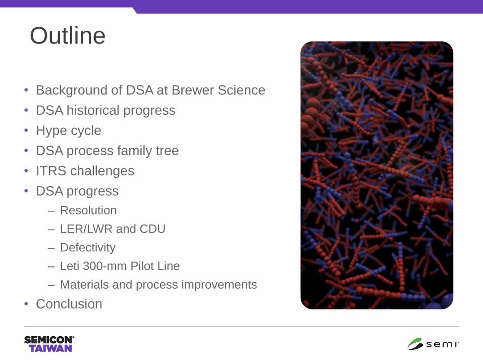
Outline
• Background of DSA at Brewer Science
• DSA historical progress
• Hype cycle
• DSA process family tree
• ITRS challenges
• DSA progress
– Resolution
– LER/LWR and CDU
– Defectivity
– Leti 300-mm Pilot Line
– Materials and process improvements
• Conclusion
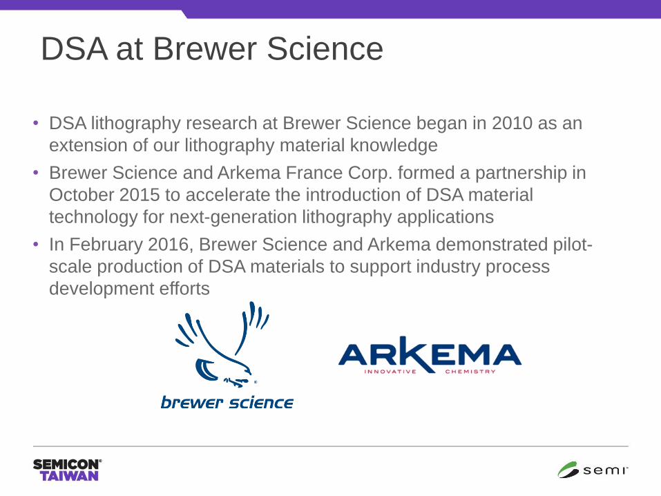
DSA at Brewer Science
• DSA lithography research at Brewer Science began in 2010 as an
extension of our lithography material knowledge
• Brewer Science and Arkema France Corp. formed a partnership in
October 2015 to accelerate the introduction of DSA material
technology for next-generation lithography applications
• In February 2016, Brewer Science and Arkema demonstrated pilot-
scale production of DSA materials to support industry process
development efforts
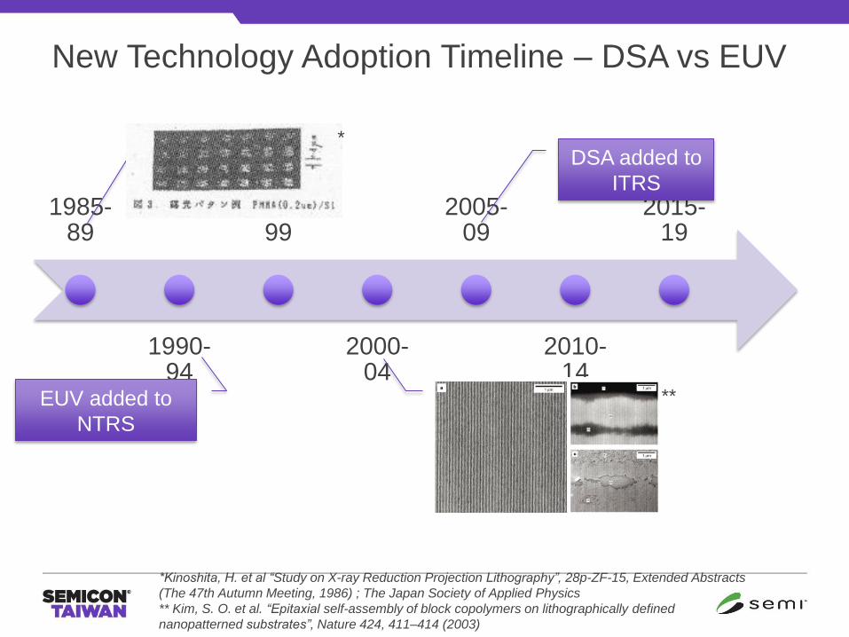
New Technology Adoption Timeline – DSA vs EUV
1985-89
1990-94
1995-99
2000-04
2005-09
2010-14
2015-19
First DSA litho
demonstration
First EUV
demonstration
DSA added to
ITRS
EUV added to
NTRS
*Kinoshita, H. et al “Study on X-ray Reduction Projection Lithography”, 28p-ZF-15, Extended Abstracts
(The 47th Autumn Meeting, 1986) ; The Japan Society of Applied Physics
** Kim, S. O. et al. “Epitaxial self-assembly of block copolymers on lithographically defined
nanopatterned substrates”, Nature 424, 411–414 (2003)
*
**
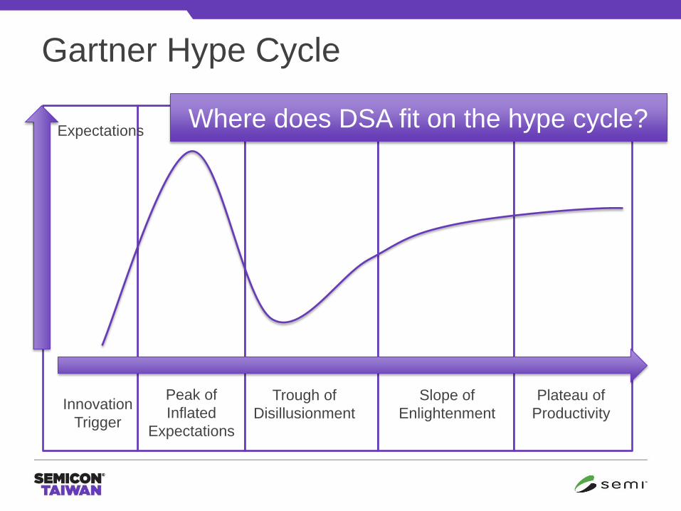
Gartner Hype Cycle
Expectations
Innovation
Trigger
Peak of
Inflated
Expectations
Trough of
Disillusionment
Slope of
Enlightenment
Plateau of
Productivity
Where does DSA fit on the hype cycle?
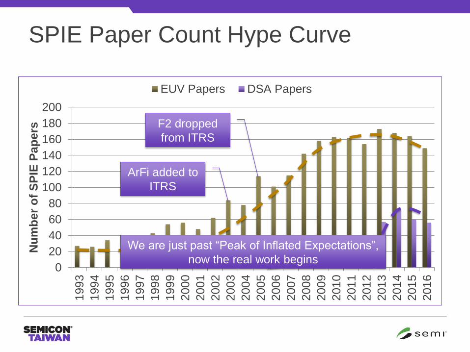
SPIE Paper Count Hype Curve
0
20
40
60
80
100
120
140
160
180
200
1993
1994
1995
1996
1997
1998
1999
2000
2001
2002
20
03
2004
2005
2006
2007
20
08
2009
2010
2011
2012
2013
2014
2015
2016
Nu
mb
er
of
SP
IE P
ap
ers
EUV Papers DSA Papers
ArFi added to
ITRS
F2 dropped
from ITRS
We are just past “Peak of Inflated Expectations”,
now the real work begins
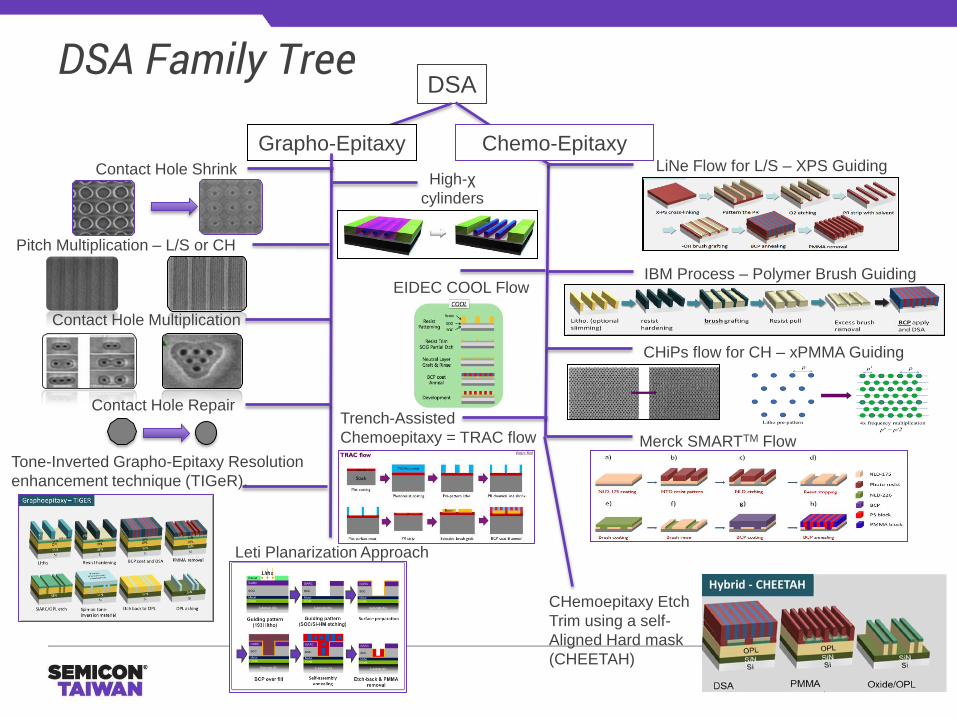
DSA Family Tree DSA
Grapho-Epitaxy Contact Hole Shrink
Pitch Multiplication – L/S or CH
Chemo-Epitaxy
Contact Hole Multiplication
Contact Hole Repair
IBM Process – Polymer Brush Guiding
High-χ
cylinders
CHiPs flow for CH – xPMMA Guiding
Merck SMARTTM Flow
LiNe Flow for L/S – XPS Guiding
EIDEC COOL Flow
Tone-Inverted Grapho-Epitaxy Resolution
enhancement technique (TIGeR).
Trench-Assisted
Chemoepitaxy = TRAC flow
CHemoepitaxy Etch
Trim using a self-
Aligned Hard mask
(CHEETAH)
Leti Planarization Approach
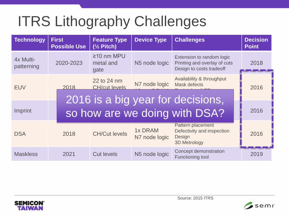
ITRS Lithography Challenges Technology First
Possible Use
Feature Type
(½ Pitch)
Device Type Challenges Decision
Point
4x Multi-
patterning 2020-2023
≥10 nm MPU
metal and
gate
N5 node logic Extension to random logic
Printing and overlay of cuts
Design to costs tradeoff 2018
EUV 2018
22 to 24 nm
CH/cut levels
18 nm LS
N7 node logic
18-nm DRAM
Availability & throughput
Mask defects
Resist dose/LER
High-NA field size
2016
Imprint 2017 14 nm LS
20 nm bit line
2D Flash
3D Flash
Defectivity
Overlay
Templates 2016
DSA 2018 CH/Cut levels 1x DRAM
N7 node logic
Pattern placement
Defectivity and inspection
Design
3D Metrology
2016
Maskless 2021 Cut levels N5 node logic Concept demonstration
Functioning tool 2019
Source: 2015 ITRS
2016 is a big year for decisions,
so how are we doing with DSA?
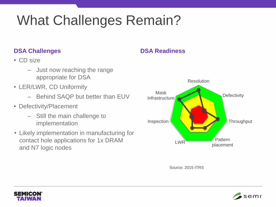
DSA Challenges
• CD size
– Just now reaching the range
appropriate for DSA
• LER/LWR, CD Uniformity
– Behind SAQP but better than EUV
• Defectivity/Placement
– Still the main challenge to
implementation
• Likely implementation in manufacturing for
contact hole applications for 1x DRAM
and N7 logic nodes
DSA Readiness
What Challenges Remain?
Resolution
Defectivity
Throughput
Patternplacement
LWR
Inspection
MaskInfrastructure
Source: 2015 ITRS
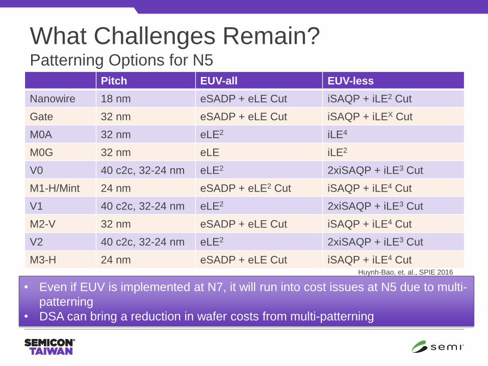
What Challenges Remain? Patterning Options for N5
• Even if EUV is implemented at N7, it will run into cost issues at N5 due to multi-
patterning
• DSA can bring a reduction in wafer costs from multi-patterning
Huynh-Bao, et. al., SPIE 2016
Pitch EUV-all EUV-less
Nanowire 18 nm eSADP + eLE Cut iSAQP + iLE2 Cut
Gate 32 nm eSADP + eLE Cut iSAQP + iLEX Cut
M0A 32 nm eLE2 iLE4
M0G 32 nm eLE iLE2
V0 40 c2c, 32-24 nm eLE2 2xiSAQP + iLE3 Cut
M1-H/Mint 24 nm eSADP + eLE2 Cut iSAQP + iLE4 Cut
V1 40 c2c, 32-24 nm eLE2 2xiSAQP + iLE3 Cut
M2-V 32 nm eSADP + eLE Cut iSAQP + iLE4 Cut
V2 40 c2c, 32-24 nm eLE2 2xiSAQP + iLE3 Cut
M3-H 24 nm eSADP + eLE Cut iSAQP + iLE4 Cut
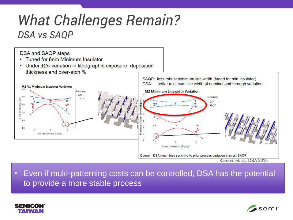
What Challenges Remain? DSA vs SAQP
• Even if multi-patterning costs can be controlled, DSA has the potential
to provide a more stable process
Kamon, et. al., DSA 2015
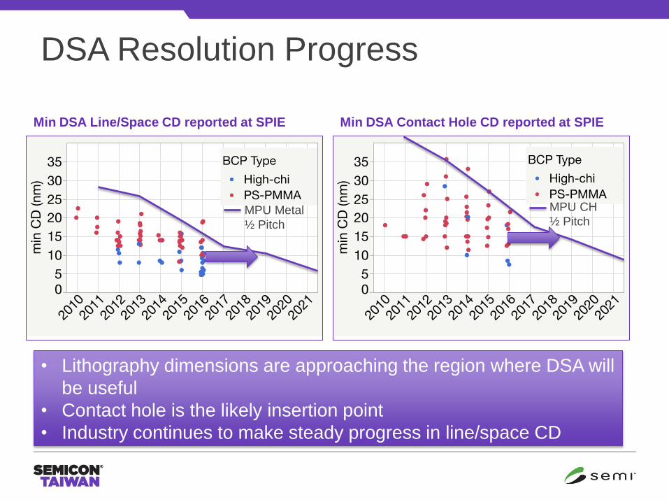
Min DSA Line/Space CD reported at SPIE Min DSA Contact Hole CD reported at SPIE
DSA Resolution Progress
• Lithography dimensions are approaching the region where DSA will
be useful
• Contact hole is the likely insertion point
• Industry continues to make steady progress in line/space CD
MPU Metal
½ Pitch
MPU CH
½ Pitch
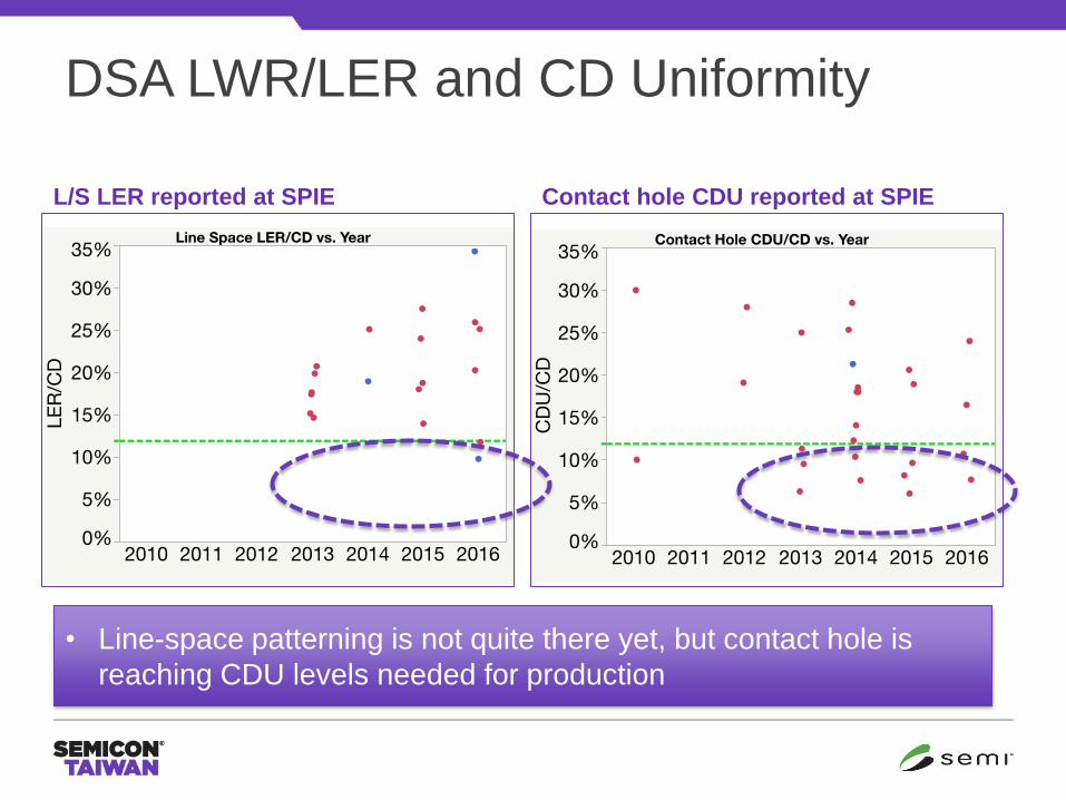
L/S LER reported at SPIE Contact hole CDU reported at SPIE
DSA LWR/LER and CD Uniformity
• Line-space patterning is not quite there yet, but contact hole is
reaching CDU levels needed for production
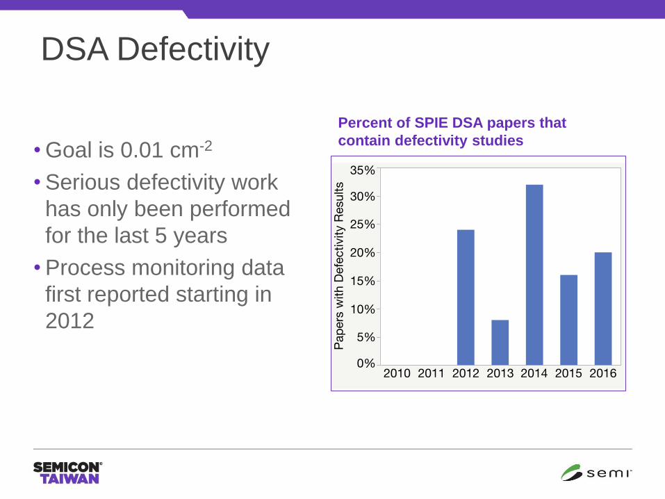
Percent of SPIE DSA papers that
contain defectivity studies
DSA Defectivity
• Goal is 0.01 cm-2
• Serious defectivity work
has only been performed
for the last 5 years
• Process monitoring data
first reported starting in
2012
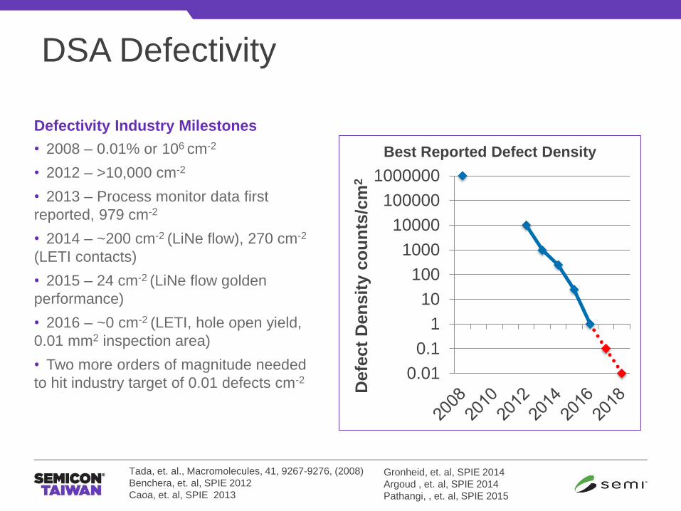
Defectivity Industry Milestones
• 2008 – 0.01% or 106 cm-2
• 2012 – >10,000 cm-2
• 2013 – Process monitor data first
reported, 979 cm-2
• 2014 – ~200 cm-2 (LiNe flow), 270 cm-2
(LETI contacts)
• 2015 – 24 cm-2 (LiNe flow golden
performance)
• 2016 – ~0 cm-2 (LETI, hole open yield,
0.01 mm2 inspection area)
• Two more orders of magnitude needed
to hit industry target of 0.01 defects cm-2
0.01
0.1
1
10
100
1000
10000
100000
1000000
Defe
ct
Den
sit
y c
ou
nts
/cm
2
Best Reported Defect Density
DSA Defectivity
Tada, et. al., Macromolecules, 41, 9267-9276, (2008)
Benchera, et. al, SPIE 2012
Caoa, et. al, SPIE 2013
Gronheid, et. al, SPIE 2014
Argoud , et. al, SPIE 2014
Pathangi, , et. al, SPIE 2015
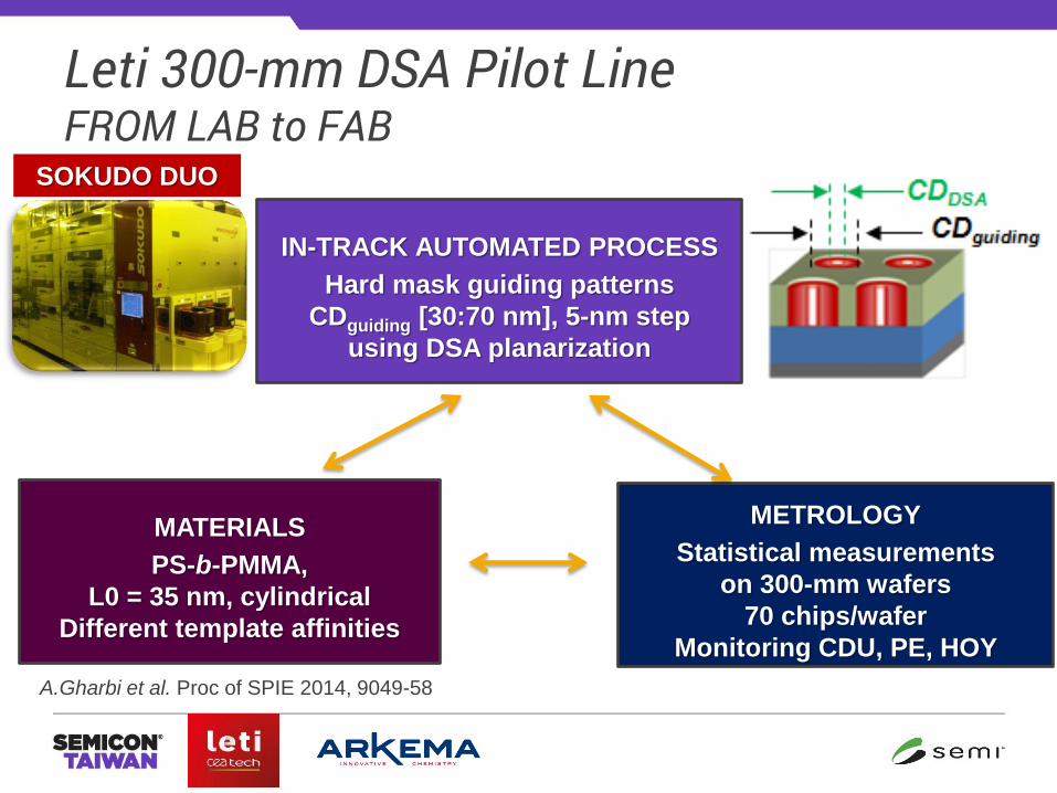
Leti 300-mm DSA Pilot Line FROM LAB to FAB
A.Gharbi et al. Proc of SPIE 2014, 9049-58
IN-TRACK AUTOMATED PROCESS
Hard mask guiding patterns
CDguiding [30:70 nm], 5-nm step
using DSA planarization
MATERIALS
PS-b-PMMA,
L0 = 35 nm, cylindrical
Different template affinities
METROLOGY
Statistical measurements
on 300-mm wafers
70 chips/wafer
Monitoring CDU, PE, HOY
SOKUDO DUO
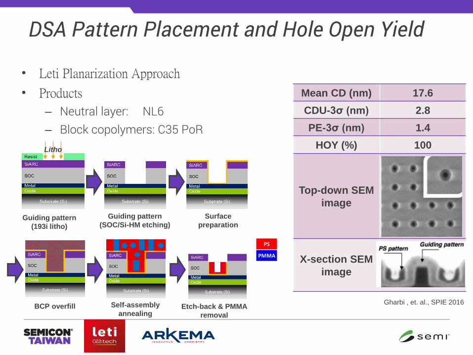
DSA Pattern Placement and Hole Open Yield
• Leti Planarization Approach
• Products
– Neutral layer: NL6 – Block copolymers: C35 PoR
PS
PMMA
Guiding pattern
(193i litho)
Guiding pattern
(SOC/Si-HM etching)
Surface
preparation
Litho
Etch-back & PMMA
removal
BCP overfill Self-assembly
annealing
Gharbi , et. al., SPIE 2016
Mean CD (nm) 17.6
CDU-3σ (nm) 2.8
PE-3σ (nm) 1.4
HOY (%) 100
Top-down SEM
image
X-section SEM
image
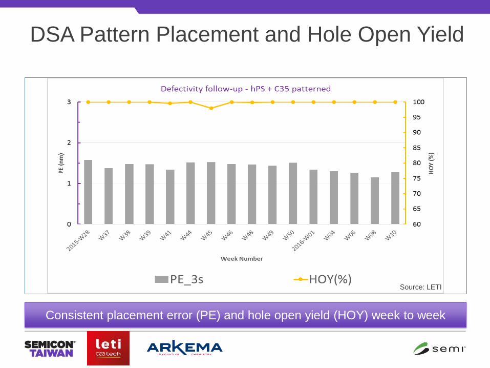
DSA Pattern Placement and Hole Open Yield
Consistent placement error (PE) and hole open yield (HOY) week to week
Source: LETI
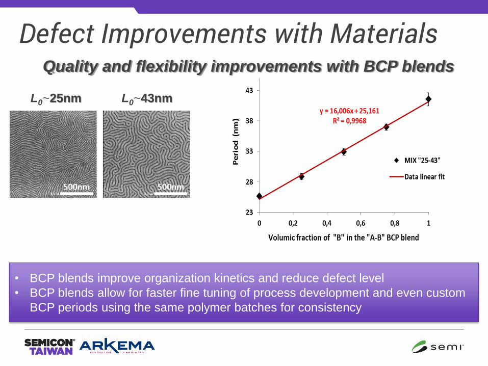
Defect Improvements with Materials
L0~25nm L0~43nm
Quality and flexibility improvements with BCP blends
• BCP blends improve organization kinetics and reduce defect level
• BCP blends allow for faster fine tuning of process development and even custom
BCP periods using the same polymer batches for consistency
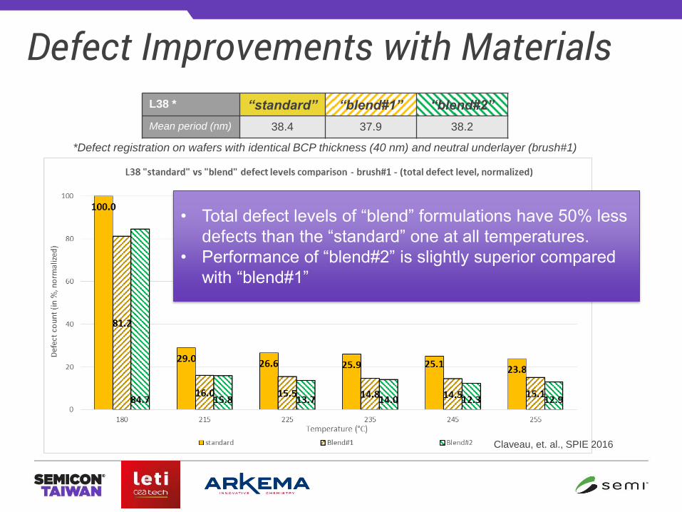
Defect Improvements with Materials L38 * “standard” “blend#1” “blend#2”
Mean period (nm) 38.4 37.9 38.2
*Defect registration on wafers with identical BCP thickness (40 nm) and neutral underlayer (brush#1)
• Total defect levels of “blend” formulations have 50% less
defects than the “standard” one at all temperatures.
• Performance of “blend#2” is slightly superior compared
with “blend#1”
Claveau, et. al., SPIE 2016
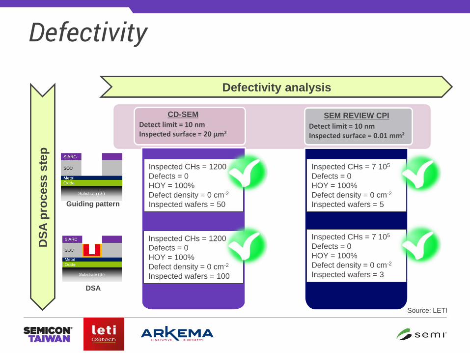
Defectivity analysis
CD-SEM
DS
A p
roces
s s
tep
Detect limit = 10 nm Inspected surface = 20 µm2
Guiding pattern
DSA
SEM REVIEW CPI
Detect limit = 10 nm Inspected surface = 0.01 mm²
Inspected CHs = 1200
Defects = 0
HOY = 100%
Defect density = 0 cm-2
Inspected wafers = 50
Inspected CHs = 7 105
Defects = 0
HOY = 100%
Defect density = 0 cm-2
Inspected wafers = 5
Inspected CHs = 1200
Defects = 0
HOY = 100%
Defect density = 0 cm-2
Inspected wafers = 100
Inspected CHs = 7 105
Defects = 0
HOY = 100%
Defect density = 0 cm-2
Inspected wafers = 3
Defectivity
Source: LETI
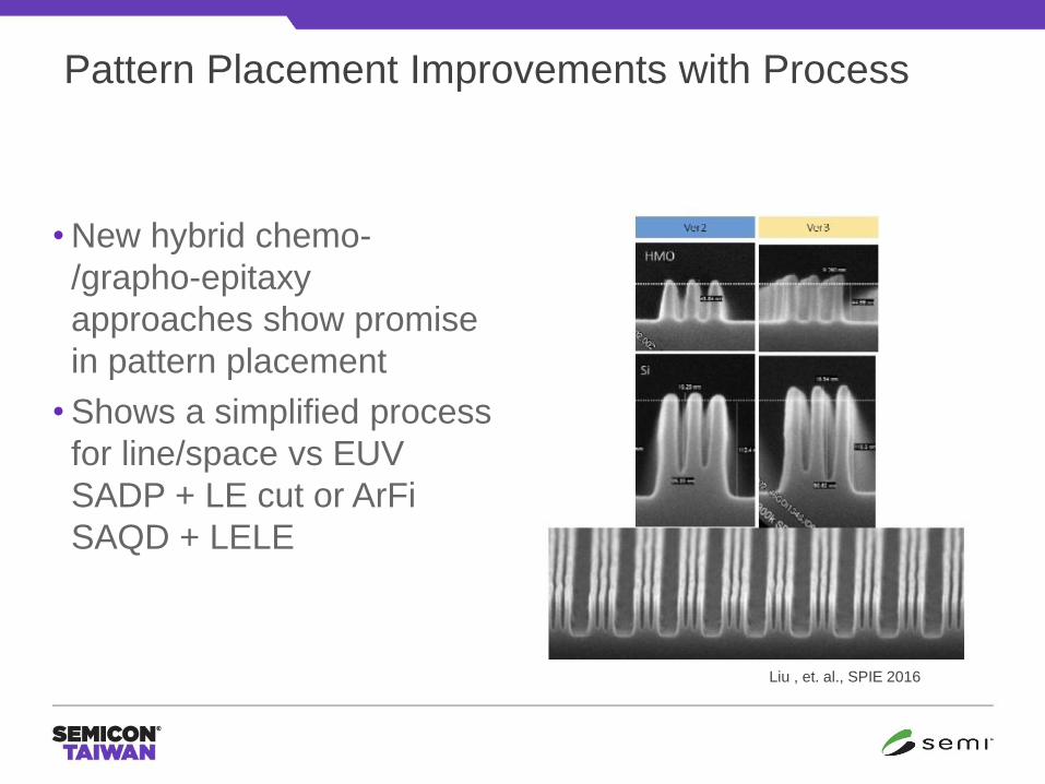
• New hybrid chemo-
/grapho-epitaxy
approaches show promise
in pattern placement
• Shows a simplified process
for line/space vs EUV
SADP + LE cut or ArFi
SAQD + LELE
Pattern Placement Improvements with Process
Liu , et. al., SPIE 2016

On the behalf of program chairs: Raluca Tiron, Roel Gronheid, Tsukasa Azuma and Joe Kline
YOU ARE WARMLY INVITED TO ATTEND
You are warmly invited to join us in Grenoble
Registration is now opened.
For more details pleas visit :
http://dsasymposium.org/
Conclusions
• DSA has moved beyond the initial
excitement of a new discovery
• DSA can easily meet resolution
requirements down to N5
• Defectivity is still the main
challenge, but the industry is
making steady, order-of-
magnitude progress each year
• Contact hole applications are the
most likely insertion point for DSA
• DSA is on track to be adopted in
manufacturing within two years
Acknowledgements:
Anthony Vander Heyden
Douglas Guerrero
Brewer Science
Ian Cayrefourcq
Christophe Navarro
Xavier Chevalier
Arkema
Raluca Tiron
cea-leti