Embed Size (px)
Citation preview
DS34C86T
www.ti.com SNLS379C –MAY 1998–REVISED APRIL 2013
DS34C86T Quad CMOS Differential Line ReceiverCheck for Samples: DS34C86T
1FEATURES DESCRIPTIONThe DS34C86T is a quad differential line receiver
2• CMOS Design for Low Powerdesigned to meet the RS-422, RS-423, and Federal
• ±0.2V Sensitivity Over the Input Common Standards 1020 and 1030 for balanced andMode Voltage Range unbalanced digital data transmission, while retaining
• Typical Propagation Delays: 19 ns the low power characteristics of CMOS.• Typical Input Hysteresis: 60 mV The DS34C86T has an input sensitivity of 200 mV
over the common mode input voltage range of ±7V.• Inputs Won't Load Line when VCC = 0VHysteresis is provided to improve noise margin and• Meets the Requirements of EIA Standard RS-discourage output instability for slowly changing input422waveforms.
• TRI-STATE Outputs for System BusThe DS34C86T features internal pull-up and pull-Compatibilitydown resistors which prevent output oscillation on
• Available in Surface Mount unused channels.• Open Input Failsafe Feature, Output High for
Separate enable pins allow independent control ofOpen Inputreceiver pairs. The TRI-STATE outputs have 6 mAsource and sink capability. The DS34C86T is pincompatible with the DS3486.
Logic Diagram
1
Please be aware that an important notice concerning availability, standard warranty, and use in critical applications ofTexas Instruments semiconductor products and disclaimers thereto appears at the end of this data sheet.
2All trademarks are the property of their respective owners.
PRODUCTION DATA information is current as of publication date. Copyright © 1998–2013, Texas Instruments IncorporatedProducts conform to specifications per the terms of the TexasInstruments standard warranty. Production processing does notnecessarily include testing of all parameters.

DS34C86T
SNLS379C –MAY 1998–REVISED APRIL 2013 www.ti.com
Connection Diagram
Top View
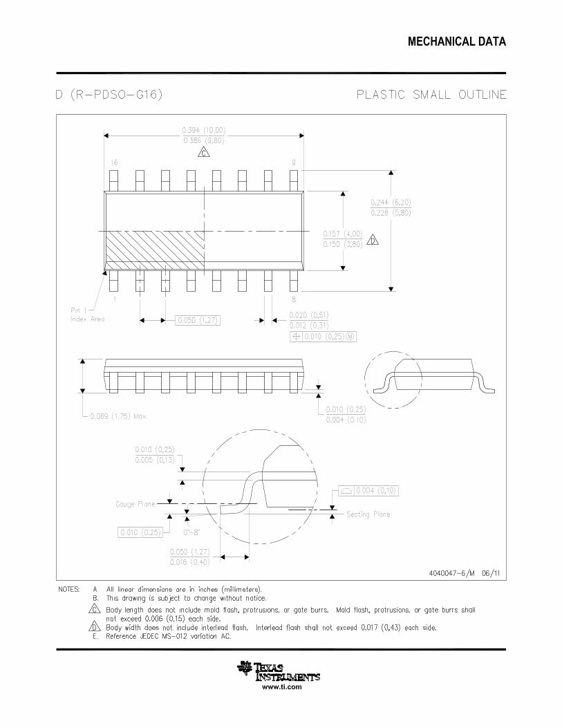
Figure 1. PDIP PackageSee Package Numbers D0016A or NFG0016E
Truth Table (1)
Enable Input Output
L X Z
H VID ≥ VTH (Max) H
H VID ≤ VTH (Min) L
H Open* H
(1) Open, not terminated. Z = TRI-STATE
These devices have limited built-in ESD protection. The leads should be shorted together or the device placed in conductive foamduring storage or handling to prevent electrostatic damage to the MOS gates.
Absolute Maximum Ratings (1) (2) (3) (4)
Supply Voltage (VCC) 7V
Input Common Mode Range (V CM) ±14V
Differential Input Voltage (V DIFF) ±14V
Enable Input Voltage (V IN) 7V
Storage Temperature Range (T STG) −65°C to +150°C
Lead Temperature (Soldering 4 sec) 260°C
Maximum Power Dissipation at 25°C (5)
PDIP Package 1645 mW
SOIC Package 1190 mW
Current Per Output ±25 mA
This device does not meet 2000V ESD rating (1)
(1) ESD Rating; HBM (1.5kΩ, 100 pF) Inputs ≥ 2000V All other pins ≥ 1000V EIAJ (0Ω, 200 pF) ≥ 350V(2) Unless otherwise specified, all voltages are referenced to ground.(3) Absolute Maximum Ratings are values beyond which the safety of the device cannot be specified. They are not meant to imply that the
device should be operated at these limits. The “Electrical Characteristics” provide conditions for actual device operation.(4) If Military/Aerospace specified devices are required, please contact the TI Sales Office/Distributors for availability and specifications.(5) Ratings apply to ambient temperature at 25°C. Above this temperature derate NFG0016E Package 13.16 mW/°C, and D0016A Package
9.52 mW/°C.
2 Submit Documentation Feedback Copyright © 1998–2013, Texas Instruments Incorporated
Product Folder Links: DS34C86T

DS34C86T
www.ti.com SNLS379C –MAY 1998–REVISED APRIL 2013
Operating ConditionsMin Max Unit
Supply Voltage (VCC) 4.50 5.50 V
Operating Temperature Range (TA) −40 +85 °C
Enable Input Rise or Fall Times 500 ns
DC Electrical Characteristics (1)
VCC = 5V ±10% (unless otherwise specified)
Parameter Test Conditions Min Typ Max Units
VTH Minimum Differential VOUT = V OH or VOL −200 35 +200 mV
Input Voltage −7V < VCM< +7V
RIN Input Resistance VIN = −7V, +7V 5.0 6.8 10 kΩ(Other Input = GND)
IIN Input Current VIN = +10V, Other Input = GND +1.1 +1.5 mA
(Under Test) VIN = −10V, Other Input = GND −2.0 −2.5 mA
VOH Minimum High Level VCC = Min., V(DIFF) = +1V 3.8 4.2 V
Output Voltage IOUT = −6.0 mA
VOL Maximum Low Level VCC = Max., V(DIFF) = −1V 0.2 0.3 V
Output Voltage IOUT = 6.0 mA
VIH Minimum Enable High2.0 V
Input Level Voltage
VIL Maximum Enable Low0.8 V
Input Level Voltage
IOZ Maximum TRI-STATE VOUT = V CC or GND, ±0.5 ±5.0 μA
Output Leakage Current TRI-STATE Control = VIL
II Maximum Enable Input VIN = V CC or GND ±1.0 μA
Current
ICC Quiescent Power VCC = Max., V(DIFF) = +1V 16 23 mA
Supply Current
VHYST Input Hysteresis VCM = 0V 60 mV
(1) Unless otherwise specified, Min/Max limits apply across the operating temperature range. All typicals are given for VCC = 5V and TA =25°C.
AC Electrical Characteristics (1)
VCC = 5V ±10% (unless otherwise specified) (Figure 2, Figure 3, Figure 4)
Parameter Test Conditions Min Typ Max Units
tPLH, Propagation Delay CL = 50 pF 19 30 nstPHL Input to Output VDIFF = 2.5V
VCM = 0V
tRISE, Output Rise and CL = 50 pF 4 9 nstFALL Fall Times VDIFF = 2.5V
VCM = 0V
tPLZ, Propagation Delay CL = 50 pF 13 18 nstPHZ ENABLE to Output RL = 1000Ω
VDIFF = 2.5V
tPZL, Propagation Delay CL = 50 pF 13 21 nstPZH ENABLE to Output RL = 1000Ω
VDIFF = 2.5V
(1) Unless otherwise specified, Min/Max limits apply across the operating temperature range. All typicals are given for VCC = 5V and TA =25°C.
Copyright © 1998–2013, Texas Instruments Incorporated Submit Documentation Feedback 3
Product Folder Links: DS34C86T
DS34C86T
SNLS379C –MAY 1998–REVISED APRIL 2013 www.ti.com
Comparison Table of Switching Characteristics into “LS-Type” Load (1)
VCC = 5V, TA = 25°C (Figure 5, Figure 6)
DS34C86 DS3486Parameter Units
Typ Max Typ Max
tPHL(D) Propagation Delay Time 17 19 nsOutput High to Low
tPLH(D) Propagation Delay Time 19 19 nsOutput Low to High
tPLZ Output Low to TRI-STATE 13 23 ns
tPHZ Output High to TRI-STATE 12 25 ns
tPZH Output TRI-STATE to High 13 18 ns
tPZL Output TRI-STATE to Low 13 20 ns
(1) This table is provided for comparison purposes only. The values in this table for the DS34C86 reflect the performance of the device butare not tested or specified.
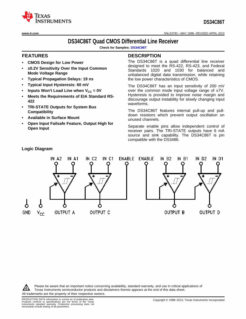
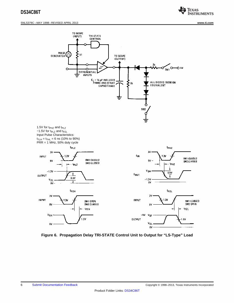
TEST AND SWITCHING WAVEFORMS
Figure 2. Propagation Delays
CL Includes load and test jig capacitance.S1 = VCC for tPZL, and tPLZ measurements.S1 = GND for tPZH, and t PHZ measurements.
Figure 3. Test Circuit for TRI-STATE Output Tests
4 Submit Documentation Feedback Copyright © 1998–2013, Texas Instruments Incorporated
Product Folder Links: DS34C86T
DS34C86T
www.ti.com SNLS379C –MAY 1998–REVISED APRIL 2013
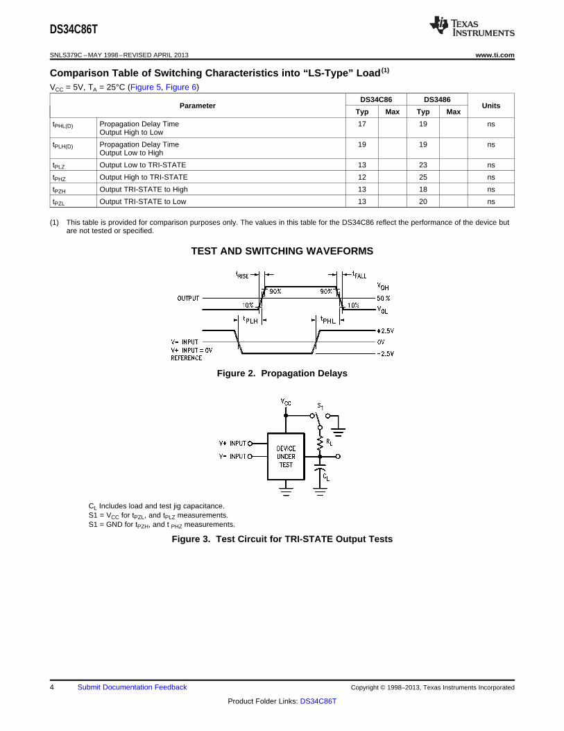
Figure 4. TRI-STATE Output Enable and Disable Waveforms
AC Test Circuits and Switching Time Waveforms
Input Pulse Characteristics:tTLH = tTHL = 6 ns (10% to 90%)PRR = 1 MHz, 50% duty cycle
Figure 5. Propagation Delay Differential Input to Output for “LS-Type” Load
Copyright © 1998–2013, Texas Instruments Incorporated Submit Documentation Feedback 5
Product Folder Links: DS34C86T
DS34C86T
SNLS379C –MAY 1998–REVISED APRIL 2013 www.ti.com
1.5V for tPHZ and tPLZ−1.5V for tPLZ and tPZLInput Pulse Characteristics:tTLH = tTHL = 6 ns (10% to 90%)PRR = 1 MHz, 50% duty cycle
tPLZ tPHZ
tPZH tPZL
Figure 6. Propagation Delay TRI-STATE Control Unit to Output for “LS-Type” Load
6 Submit Documentation Feedback Copyright © 1998–2013, Texas Instruments Incorporated
Product Folder Links: DS34C86T
DS34C86T
www.ti.com SNLS379C –MAY 1998–REVISED APRIL 2013
REVISION HISTORY
Changes from Revision B (April 2013) to Revision C Page
• Changed layout of National Data Sheet to TI format ............................................................................................................ 6
Copyright © 1998–2013, Texas Instruments Incorporated Submit Documentation Feedback 7
Product Folder Links: DS34C86T
PACKAGE OPTION ADDENDUM
www.ti.com 23-Aug-2017
Addendum-Page 1
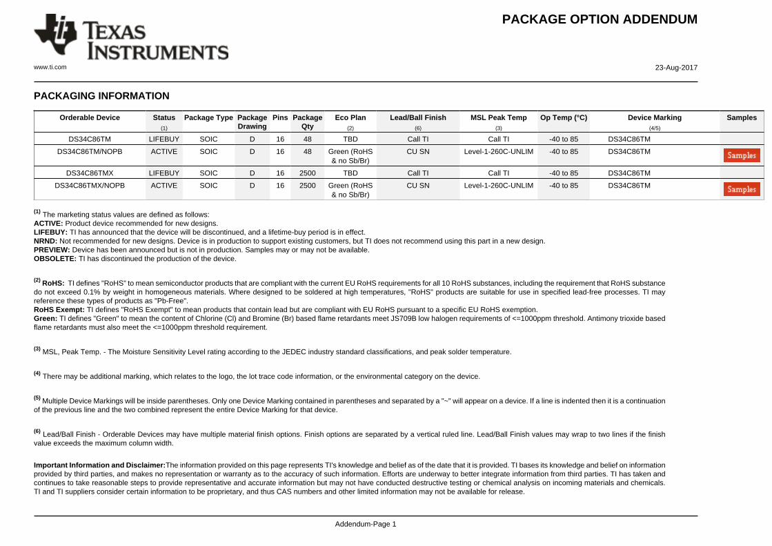
PACKAGING INFORMATION
Orderable Device Status(1)
Package Type PackageDrawing
Pins PackageQty
Eco Plan(2)
Lead/Ball Finish(6)
MSL Peak Temp(3)
Op Temp (°C) Device Marking(4/5)
Samples
DS34C86TM LIFEBUY SOIC D 16 48 TBD Call TI Call TI -40 to 85 DS34C86TM
DS34C86TM/NOPB ACTIVE SOIC D 16 48 Green (RoHS& no Sb/Br)
CU SN Level-1-260C-UNLIM -40 to 85 DS34C86TM
DS34C86TMX LIFEBUY SOIC D 16 2500 TBD Call TI Call TI -40 to 85 DS34C86TM
DS34C86TMX/NOPB ACTIVE SOIC D 16 2500 Green (RoHS& no Sb/Br)
CU SN Level-1-260C-UNLIM -40 to 85 DS34C86TM
(1) The marketing status values are defined as follows:ACTIVE: Product device recommended for new designs.LIFEBUY: TI has announced that the device will be discontinued, and a lifetime-buy period is in effect.NRND: Not recommended for new designs. Device is in production to support existing customers, but TI does not recommend using this part in a new design.PREVIEW: Device has been announced but is not in production. Samples may or may not be available.OBSOLETE: TI has discontinued the production of the device.
(2) RoHS: TI defines "RoHS" to mean semiconductor products that are compliant with the current EU RoHS requirements for all 10 RoHS substances, including the requirement that RoHS substancedo not exceed 0.1% by weight in homogeneous materials. Where designed to be soldered at high temperatures, "RoHS" products are suitable for use in specified lead-free processes. TI mayreference these types of products as "Pb-Free".RoHS Exempt: TI defines "RoHS Exempt" to mean products that contain lead but are compliant with EU RoHS pursuant to a specific EU RoHS exemption.Green: TI defines "Green" to mean the content of Chlorine (Cl) and Bromine (Br) based flame retardants meet JS709B low halogen requirements of <=1000ppm threshold. Antimony trioxide basedflame retardants must also meet the <=1000ppm threshold requirement.
(3) MSL, Peak Temp. - The Moisture Sensitivity Level rating according to the JEDEC industry standard classifications, and peak solder temperature.
(4) There may be additional marking, which relates to the logo, the lot trace code information, or the environmental category on the device.
(5) Multiple Device Markings will be inside parentheses. Only one Device Marking contained in parentheses and separated by a "~" will appear on a device. If a line is indented then it is a continuationof the previous line and the two combined represent the entire Device Marking for that device.
(6) Lead/Ball Finish - Orderable Devices may have multiple material finish options. Finish options are separated by a vertical ruled line. Lead/Ball Finish values may wrap to two lines if the finishvalue exceeds the maximum column width.
Important Information and Disclaimer:The information provided on this page represents TI's knowledge and belief as of the date that it is provided. TI bases its knowledge and belief on informationprovided by third parties, and makes no representation or warranty as to the accuracy of such information. Efforts are underway to better integrate information from third parties. TI has taken andcontinues to take reasonable steps to provide representative and accurate information but may not have conducted destructive testing or chemical analysis on incoming materials and chemicals.TI and TI suppliers consider certain information to be proprietary, and thus CAS numbers and other limited information may not be available for release.
PACKAGE OPTION ADDENDUM
www.ti.com 23-Aug-2017
Addendum-Page 2
In no event shall TI's liability arising out of such information exceed the total purchase price of the TI part(s) at issue in this document sold by TI to Customer on an annual basis.
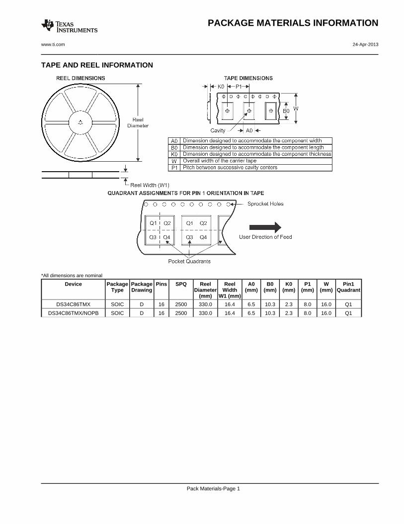
TAPE AND REEL INFORMATION
*All dimensions are nominal
Device PackageType
PackageDrawing
Pins SPQ ReelDiameter
(mm)
ReelWidth
W1 (mm)
A0(mm)
B0(mm)
K0(mm)
P1(mm)
W(mm)
Pin1Quadrant
DS34C86TMX SOIC D 16 2500 330.0 16.4 6.5 10.3 2.3 8.0 16.0 Q1
DS34C86TMX/NOPB SOIC D 16 2500 330.0 16.4 6.5 10.3 2.3 8.0 16.0 Q1
PACKAGE MATERIALS INFORMATION
www.ti.com 24-Apr-2013
Pack Materials-Page 1
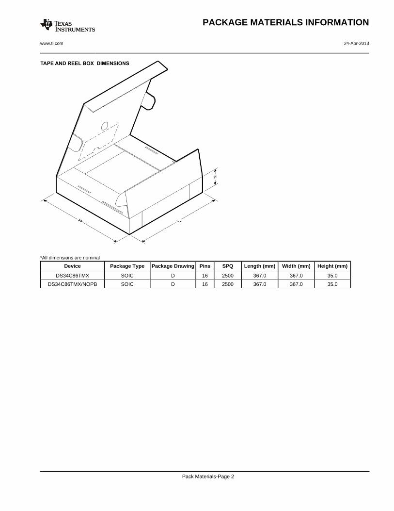
*All dimensions are nominal
Device Package Type Package Drawing Pins SPQ Length (mm) Width (mm) Height (mm)
DS34C86TMX SOIC D 16 2500 367.0 367.0 35.0
DS34C86TMX/NOPB SOIC D 16 2500 367.0 367.0 35.0
PACKAGE MATERIALS INFORMATION
www.ti.com 24-Apr-2013
Pack Materials-Page 2

IMPORTANT NOTICE
Texas Instruments Incorporated (TI) reserves the right to make corrections, enhancements, improvements and other changes to itssemiconductor products and services per JESD46, latest issue, and to discontinue any product or service per JESD48, latest issue. Buyersshould obtain the latest relevant information before placing orders and should verify that such information is current and complete.TI’s published terms of sale for semiconductor products (http://www.ti.com/sc/docs/stdterms.htm) apply to the sale of packaged integratedcircuit products that TI has qualified and released to market. Additional terms may apply to the use or sale of other types of TI products andservices.Reproduction of significant portions of TI information in TI data sheets is permissible only if reproduction is without alteration and isaccompanied by all associated warranties, conditions, limitations, and notices. TI is not responsible or liable for such reproduceddocumentation. Information of third parties may be subject to additional restrictions. Resale of TI products or services with statementsdifferent from or beyond the parameters stated by TI for that product or service voids all express and any implied warranties for theassociated TI product or service and is an unfair and deceptive business practice. TI is not responsible or liable for any such statements.Buyers and others who are developing systems that incorporate TI products (collectively, “Designers”) understand and agree that Designersremain responsible for using their independent analysis, evaluation and judgment in designing their applications and that Designers havefull and exclusive responsibility to assure the safety of Designers' applications and compliance of their applications (and of all TI productsused in or for Designers’ applications) with all applicable regulations, laws and other applicable requirements. Designer represents that, withrespect to their applications, Designer has all the necessary expertise to create and implement safeguards that (1) anticipate dangerousconsequences of failures, (2) monitor failures and their consequences, and (3) lessen the likelihood of failures that might cause harm andtake appropriate actions. Designer agrees that prior to using or distributing any applications that include TI products, Designer willthoroughly test such applications and the functionality of such TI products as used in such applications.TI’s provision of technical, application or other design advice, quality characterization, reliability data or other services or information,including, but not limited to, reference designs and materials relating to evaluation modules, (collectively, “TI Resources”) are intended toassist designers who are developing applications that incorporate TI products; by downloading, accessing or using TI Resources in anyway, Designer (individually or, if Designer is acting on behalf of a company, Designer’s company) agrees to use any particular TI Resourcesolely for this purpose and subject to the terms of this Notice.TI’s provision of TI Resources does not expand or otherwise alter TI’s applicable published warranties or warranty disclaimers for TIproducts, and no additional obligations or liabilities arise from TI providing such TI Resources. TI reserves the right to make corrections,enhancements, improvements and other changes to its TI Resources. TI has not conducted any testing other than that specificallydescribed in the published documentation for a particular TI Resource.Designer is authorized to use, copy and modify any individual TI Resource only in connection with the development of applications thatinclude the TI product(s) identified in such TI Resource. NO OTHER LICENSE, EXPRESS OR IMPLIED, BY ESTOPPEL OR OTHERWISETO ANY OTHER TI INTELLECTUAL PROPERTY RIGHT, AND NO LICENSE TO ANY TECHNOLOGY OR INTELLECTUAL PROPERTYRIGHT OF TI OR ANY THIRD PARTY IS GRANTED HEREIN, including but not limited to any patent right, copyright, mask work right, orother intellectual property right relating to any combination, machine, or process in which TI products or services are used. Informationregarding or referencing third-party products or services does not constitute a license to use such products or services, or a warranty orendorsement thereof. Use of TI Resources may require a license from a third party under the patents or other intellectual property of thethird party, or a license from TI under the patents or other intellectual property of TI.TI RESOURCES ARE PROVIDED “AS IS” AND WITH ALL FAULTS. TI DISCLAIMS ALL OTHER WARRANTIES ORREPRESENTATIONS, EXPRESS OR IMPLIED, REGARDING RESOURCES OR USE THEREOF, INCLUDING BUT NOT LIMITED TOACCURACY OR COMPLETENESS, TITLE, ANY EPIDEMIC FAILURE WARRANTY AND ANY IMPLIED WARRANTIES OFMERCHANTABILITY, FITNESS FOR A PARTICULAR PURPOSE, AND NON-INFRINGEMENT OF ANY THIRD PARTY INTELLECTUALPROPERTY RIGHTS. TI SHALL NOT BE LIABLE FOR AND SHALL NOT DEFEND OR INDEMNIFY DESIGNER AGAINST ANY CLAIM,INCLUDING BUT NOT LIMITED TO ANY INFRINGEMENT CLAIM THAT RELATES TO OR IS BASED ON ANY COMBINATION OFPRODUCTS EVEN IF DESCRIBED IN TI RESOURCES OR OTHERWISE. IN NO EVENT SHALL TI BE LIABLE FOR ANY ACTUAL,DIRECT, SPECIAL, COLLATERAL, INDIRECT, PUNITIVE, INCIDENTAL, CONSEQUENTIAL OR EXEMPLARY DAMAGES INCONNECTION WITH OR ARISING OUT OF TI RESOURCES OR USE THEREOF, AND REGARDLESS OF WHETHER TI HAS BEENADVISED OF THE POSSIBILITY OF SUCH DAMAGES.Unless TI has explicitly designated an individual product as meeting the requirements of a particular industry standard (e.g., ISO/TS 16949and ISO 26262), TI is not responsible for any failure to meet such industry standard requirements.Where TI specifically promotes products as facilitating functional safety or as compliant with industry functional safety standards, suchproducts are intended to help enable customers to design and create their own applications that meet applicable functional safety standardsand requirements. Using products in an application does not by itself establish any safety features in the application. Designers mustensure compliance with safety-related requirements and standards applicable to their applications. Designer may not use any TI products inlife-critical medical equipment unless authorized officers of the parties have executed a special contract specifically governing such use.Life-critical medical equipment is medical equipment where failure of such equipment would cause serious bodily injury or death (e.g., lifesupport, pacemakers, defibrillators, heart pumps, neurostimulators, and implantables). Such equipment includes, without limitation, allmedical devices identified by the U.S. Food and Drug Administration as Class III devices and equivalent classifications outside the U.S.TI may expressly designate certain products as completing a particular qualification (e.g., Q100, Military Grade, or Enhanced Product).Designers agree that it has the necessary expertise to select the product with the appropriate qualification designation for their applicationsand that proper product selection is at Designers’ own risk. Designers are solely responsible for compliance with all legal and regulatoryrequirements in connection with such selection.Designer will fully indemnify TI and its representatives against any damages, costs, losses, and/or liabilities arising out of Designer’s non-compliance with the terms and provisions of this Notice.
Mailing Address: Texas Instruments, Post Office Box 655303, Dallas, Texas 75265Copyright © 2017, Texas Instruments Incorporated