Embed Size (px)
Citation preview
MYTNA1R84RELA2RA Document Category: Datasheet
UltraBK™ 4A DC–DC Converter Module
http://www.murata.com/products/power Copyright ©2020 Murata Manufacturing Co., Ltd. All rights reserved. Export Control Code : X0863 Document No :D90DH – 00072 MYTNA1R84RELA2RA A01 Page 1 of 26
Product Description The MYTNA1R84RELA2RA is miniature UltraBK™ called “Ultra Block”, an ultra-thin high efficiency integrated power solution that combines a 4A DC/DC converter with components.
This totally integrated module provides up to 90.5% efficiency in a small and thin 10.5 x 9.0 x 2.1mm LGA package. Murata’s easy-to-use module terminal design allows simple power layout and maximum efficiency by minimizing routing parasitic resistance.
■ Wide input voltage 6.0 to 14.4V■ Settable output voltage 0.7 to 1.8V■ Efficiency up to 90.5%
Up to 90.0% Efficiency with 12VIN/1.8VOUT/4A■ Up to 4A■ Ultra-thin/small 10.5 x 9.0 x 2.1mm LGA
package
Features ■ Power-good output■ Over-current and Over-temperature protection■ Remote on/off control■ Output voltage sense
Typical Applications ■ PCIe / server applications■ FPGA and DSP■ Datacom / telecom systems■ Distributed bus architectures (DBA)■ Programmable logic and mixed voltage systems
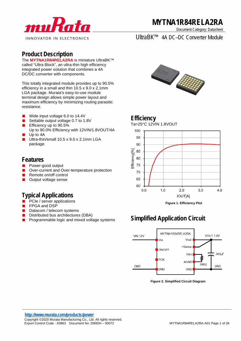
Efficiency Ta=25°C 12VIN 1.8VOUT
Figure 1. Efficiency Plot
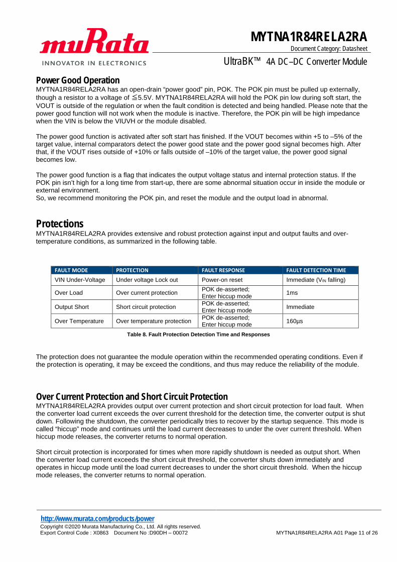
Simplified Application Circuit
Figure 2. Simplified Circuit Diagram

MYTNA1R84RELA2RA Document Category: Datasheet
UltraBK™ 4A DC–DC Converter Module
http://www.murata.com/products/power Copyright ©2020 Murata Manufacturing Co., Ltd. All rights reserved. Export Control Code : X0863 Document No :D90DH – 00072
MYTNA1R84RELA2RA A01 Page 2 of 26
Product Description ...........................................................1 Features ...........................................................................1 Typical Applications ...........................................................1 Efficiency .........................................................................1 Simplified Application Circuit ..............................................1 Absolute Maximum Ratings(1)(2) ............................................3 Recommended Operating Conditions(1) .................................3 Package Thermal Characteristics(1)(2) ....................................3 Electrical Characteristics ....................................................4 Pin Configuration ...............................................................5 Pin Descriptions ................................................................6 Functional Block Diagram ...................................................6 Typical Performance Characteristics ....................................7 Thermal Deratings (Reference Data) .....................................8 Output Voltage Range ........................................................8 Limitation of Input Voltage Slew rate.....................................9 Detailed Description ...........................................................9 Output Voltage Adjustment ............................................................................... 9 Resistor Trim Equation...................................................................................... 9 Output Voltage Remote Sense Function ........................................................ 10 Remote Enable Function ................................................................................ 10 Soft start Function ........................................................................................... 10 Power Good Operation ................................................................................... 11 Protections ..................................................................... 11 Over Current Protection and Short Circuit Protection..................................... 11 Over Temperature Protection ......................................................................... 12 Soldering Guidelines ........................................................ 12 Pb-free Solder Processes ............................................................................... 13 Dry Pack Information ........................................................ 13 Application Performance ........................................... 14 Transient Performance ..................................................... 17 Test Circuit ..................................................................... 17 Component Selection ....................................................... 18 Input Fuse ....................................................................................................... 18 Input Capacitor ................................................................................................ 18 Output Capacitor ............................................................................................. 18 Packaging Information ...................................................... 19 Moisture Sensitivity Level ............................................................................... 19 Package Drawing ............................................................................................ 19 Recommended Board Land Pattern (Top View) ............................................. 19 Top Marking Specification ............................................................................... 20 Application Circuit ........................................................... 20 Application Circuit Part List (Recommended) ....................... 20 Application Board Example ............................................... 21 Tape and Reel Specification .............................................. 22 Order Codes ................................................................... 24
Notices .......................................................................... 24
CAUTION ................................................................ 24 Limitation of Applications ................................................................................ 24
Note ...................................................................................................... 24 Product Specification ...................................................................................... 25 Sales contact .................................................................................................. 25 Disclaimers .................................................................... 25 Patent Statement ............................................................................................ 26 Copyright and Trademark ................................................. 26

MYTNA1R84RELA2RA Document Category: Datasheet
UltraBK™ 4A DC–DC Converter Module
http://www.murata.com/products/power Copyright ©2020 Murata Manufacturing Co., Ltd. All rights reserved. Export Control Code : X0863 Document No :D90DH – 00072
MYTNA1R84RELA2RA A01 Page 3 of 26
Absolute Maximum Ratings(1)(2) PARAMETER MIN MAX UNITS Vin, ON/OFF Pin(3) -0.3 16 V Trim(4), POK Pin -0.3 5.5 V Storage Temperature -40 125 °C Soldering / Reflow temperature(5) - 260 °C ESD Tolerance, HBM(6) - 1000 V Notes:
(1) Stresses beyond those listed under absolute maximum ratings may cause permanent damage to the device. These are stress ratings only. Functional operation of the device at these or any other conditions beyond those indicated in the operational sections of the specification are not implied. Exposure to absolute maximum rating conditions for extended periods may extremely reduce device reliability.
(2) All voltages are with respect to GND plane. (3) Do NOT exceed more than 0.3V from Vin voltage. (4) The Trim pin is designed to be connected to GND via a resistor. (5) Recommended Reflow profile is written in “Soldering Guidelines”. (6) Human body model, per the JEDEC standard JS-001-2012.
Table 1. Absolute Maximum Ratings
Recommended Operating Conditions(1) PARAMETER MIN MAX UNITS Input Voltage Range 6.0 14.4 V Ambient Temperature(2) -40 105 °C Junction Temperature -40 120 °C Load Current 0 4 A Notes: (1) This module should be operated inside the recommended operating conditions. This module has been designed and tested on the
assumption that it will be used under the recommended operating conditions. Operating in not recommended condition may reduce reliability of the module.
(2) See the temperature derating curves in the thermal deratings. However, do not condensate.
Table 2. Recommended Operating Conditions
Package Thermal Characteristics(1)(2) PARAMETER TYP UNITS Θjcb-1 Junction-case-bottom at heat Junction1 10.0 °C/W Θjcb-2 Junction-case-bottom at heat Junction2 47.3 °C/W Θjct-1 Junction-case-top a heat Junction1 64.9 °C/W Θjct-2 Junction-case-top a heat Junction2 53.7 °C/W Θja Junction-air 19.9 °C/W Notes: (1) Package thermal characteristics and performance are acquire and reported in according to the JEDEC standard JESD51-12. See
“Fig.34” below for more information on our measurement conditions. (2) Junction thermal resistance is a function not only of the internal parts, but it is also extremely sensitive to the environment which
includes, but is not limited to, board thickness, number of layers, copper weight / routes, and air flow. Attention to the board layout is necessary to realize expected thermal performance.
Table 3. Package Thermal Characteristics

MYTNA1R84RELA2RA Document Category: Datasheet
UltraBK™ 4A DC–DC Converter Module
http://www.murata.com/products/power Copyright ©2020 Murata Manufacturing Co., Ltd. All rights reserved. Export Control Code : X0863 Document No :D90DH – 00072
MYTNA1R84RELA2RA A01 Page 4 of 26
Electrical Characteristics VIN=12V, VOUT=1.8V, IOUT=4A, Ta=+25°C, unless otherwise noted. The Electrical Characteristics table is based on the test circuit in Figure 29.
PARAMETER SYMBOL CONDITIONS MIN TYP MAX UNITS INPUT SUPPLY Input Voltage(1) VIN 6 12 14.4 V Input Voltage Start-up Slew rate(3) VINSR Note(2) - 150 V/ms
VIN Under Voltage Lockout Threshold - VIN rising(3) VIUVH - - 5.45 V
VIN Under Voltage Lockout Threshold - VIN falling(3) VIUVL 4.5 - - V
VIN Under Voltage Lockout Hysteresis VIUVHYS - 215 - mV
VIN Current Supply, Switching IVINSW No Load - 25 - mA VIN Current Supply, Shutdown IVINSD VOUT=0V, ON/OFF=0V - 130 - µA Remote ON/OFF Control (ON/OFF Pin) Threshold High(3) VTREH Logic ON by pull-up or open of
ON/OFF Pin 1.1 - - V
Threshold Low(3) VTREL Logic OFF by pull-down of ON/OFF Pin - - 0.4 V
ON/OFF Pin Leakage Current(3) ILEN VIN=14.4V, ON/OFF=0V, From Vin to ON/OFF - - 200 µA
CONVERTER
Efficiency EFF
VIN=12.0V, VOUT=1.8V, IOUT=4A - 90 - %
VIN=12.0V, VOUT=1.2V, IOUT=4A - 88 - %
Charge Pump Switching Frequency Per a phase - 500 - kHz
Buck Converter Switching Frequency Per a phase - 1000 - kHz
Startup Time VOUT=5 to 95% of VOUT - 4 - msec POWER GOOD (POK Pin) POK Sink Current(3) POK=0.4V 4 - - mA POK Pin Leakage Current(3) ILPG POK=5V, POK=High - - 1 µA
POK & Output Under-Voltage VOUT falling (fault) - 90 - % of
VOUT VOUT rising (good) - 95 -
POK & Output Over-Voltage VOUT rising (fault) - 110 - VOUT falling (good) - 105 -
THERMAL SHUTDOWN Thermal Shutdown Threshold TSD Shutdown operating - 150 - °C Thermal Shutdown Hysteresis TSDHYS - 20 - °C OUTPUT
Output Voltage(4) VOUT 9.6 ≤ VIN ≤ 14.4V 0.7 - 1.8 V 7.0 ≤ VIN ≤ 14.4V 0.7 - 1.35 V 6.0 ≤ VIN ≤ 14.4V 0.7 - 1.0 V
Output Voltage Accuracy (1)(5) 6.0 ≤ VIN ≤ 14.4V 0.7 ≤ VOUT ≤ 1.8V(4) 0 ≤ IOUT ≤ 4A
-3 - +3 %
Temperature variation(3) -40 ≤ Ta ≤ 105°C - 1 - %
Total Output Voltage Accuracy(3) 0.7 ≤ VOUT ≤ 1.8V(4) 0 ≤ IOUT ≤ 4A -40 ≤ Ta ≤ 105°C
-3 - +3 %
Output Current(1) IOUT 0 - 4 A Current Limit Inception - 11 - A Current Limit Method Hiccup

MYTNA1R84RELA2RA Document Category: Datasheet
UltraBK™ 4A DC–DC Converter Module
http://www.murata.com/products/power Copyright ©2020 Murata Manufacturing Co., Ltd. All rights reserved. Export Control Code : X0863 Document No :D90DH – 00072
MYTNA1R84RELA2RA A01 Page 5 of 26
VIN=12V, VOUT=1.8V, IOUT=4A, Ta=+25°C, unless otherwise noted. The Electrical Characteristics table is based on the test circuit in Figure 29.
PARAMETER SYMBOL CONDITIONS MIN TYP MAX UNITS Line Regulation(3)(5) VIN=min. to max. -1 - +1 % Load Regulation(3)(5) IOUT=min. to max. -1 - +1 % Dynamic Load Peak Deviation IOUT=50-100%, SR=1.0A/µs - ±3.0 - %
Ripple and Noise(2)(3) (20MHz bandwidth)
6.0 ≤ VIN ≤ 14.4V 0.7 ≤ VOUT ≤ 1.8V(4) 0 ≤ IOUT ≤ 4A
- - 40 mV pk-pk
VIN=12.0V 0.7 ≤ VOUT ≤ 1.8V(4) IOUT=4A
- 1 - % of Vout
External Output Capacitance Range(2) COUT 200 - 2000 µF Notes: (1) Min/Max specifications are 100% production tested at Ta=25°C, unless otherwise noted. Limits over the operating range are
guaranteed by design. (2) See the section of “Limitation of Input Voltage slew rate”. (3) Guaranteed by design. (4) See the Output Voltage Range of fig.9. (5) Only statics state.
Table 4. Electrical Characteristics
Pin Configuration
Figure 3. Module Terminal (Top View)
1 2 3 4 5 6
A B C D E F G H

MYTNA1R84RELA2RA Document Category: Datasheet
UltraBK™ 4A DC–DC Converter Module
http://www.murata.com/products/power Copyright ©2020 Murata Manufacturing Co., Ltd. All rights reserved. Export Control Code : X0863 Document No :D90DH – 00072
MYTNA1R84RELA2RA A01 Page 6 of 26
Pin Descriptions
PIN NO. NAME DESCRIPTION
A1-A3, B2-B3 Vin Input Voltage pins. Apply input voltage between these pins and GND pins.
A4-A6, B4-B6, C2-C5, D2-D5,E2-E5, F2-F5, G1-G3, H1-H3
GND Ground pins. Connect to the GND plane.
B1 ON/OFF Remote ON/OFF pin. This pin is connected to Vin through the internal resistance.
C1 POK Power Good pin. The function is operated by internal open-drain FET.
C6, D6, E6, F6, G6 DNC Do not connect pins. Those pins must be left floating individually.
D1 Trim Trimming pin. Connect to the resistor to adjust to the target output voltage.
E1 AGND Analog ground pin. Connect to trimming Resistor.
F1 +Sense
Output Voltage Sensing pin. Connect to an output near the load to improve load regulation. This pin must be connected to output near the load, or at the module pins.
G4-G5, H4-H6 Vout
Output pins. Connect the output load between these pins and Ground pins. Place external bypass capacitors as close as possible to these pins to reduce parasitic inductance.
Table 5. Pin Descriptions
Functional Block Diagram
Figure 4. Functional Block Diagram

MYTNA1R84RELA2RA Document Category: Datasheet
UltraBK™ 4A DC–DC Converter Module
http://www.murata.com/products/power Copyright ©2020 Murata Manufacturing Co., Ltd. All rights reserved. Export Control Code : X0863 Document No :D90DH – 00072
MYTNA1R84RELA2RA A01 Page 7 of 26
Typical Performance Characteristics (VIN=12V Ta=25°C)
Figure 5. Efficiency vs. Load Current and Output Voltage
Figure 6. Output Ripple vs. Load Current and Output Voltage (COUT=200µF, ScopeBW=20MHz)
Figure 7. Power Dissipation vs. Load Current and Output Voltage

MYTNA1R84RELA2RA Document Category: Datasheet
UltraBK™ 4A DC–DC Converter Module
http://www.murata.com/products/power Copyright ©2020 Murata Manufacturing Co., Ltd. All rights reserved. Export Control Code : X0863 Document No :D90DH – 00072
MYTNA1R84RELA2RA A01 Page 8 of 26
Thermal Deratings (Reference Data)
Figure 8. Thermal Deratings (VIN =12V)
Thermal deratings are evaluated in following condition. ・The product is mounted on 114.5 x 101.5 x 1.6mm (Layer1, 4: 2oz Layer2, 3: 1oz copper) FR-4 board. ・No forced air flow. Surface temperature of the product: 118.7°C max.
Output Voltage Range
Figure 9. Output Voltage Range

MYTNA1R84RELA2RA Document Category: Datasheet
UltraBK™ 4A DC–DC Converter Module
http://www.murata.com/products/power Copyright ©2020 Murata Manufacturing Co., Ltd. All rights reserved. Export Control Code : X0863 Document No :D90DH – 00072
MYTNA1R84RELA2RA A01 Page 9 of 26
Limitation of Input Voltage Slew rate When starting the module with ramping Input Voltage up, the slew rate of the ramping should be managed for the proper operation. If Input Voltage ramping up is too steep, it would cause charge injection to the internal nodes via parasitic. The maximum slew rate of the Input Voltage ramp up when booting the module with Input Voltage is specified on the table 4 "Electronic Characteristics". Similarly, if the VIN slew late is too low compare with VOUT slew rate, it could prevent expected start-up behavior. To avoid hitting the maximum duty cycle operation, the VIN slew rate should satisfy the equation of (eq.1). As a reference, estimated value of the slew rate and start-up time for each output voltage is written in the follow table. VINSR_L is minimum of input voltage start-up slew rate.
VINSR [V/ms] ≧ 0.2 × 𝑉𝑉𝑉𝑉𝑉𝑉𝑉𝑉[𝑉𝑉] − 0.1 (eq.1)
Table.6 Minimum input voltage start-up slew rate and start-up time
Detailed Description The MYTNA1R84RELA2RA is a two-stage DCDC converter that is composed of a dual-phase charge pump-based DCDC converter and a dual-phase synchronous buck DCDC converter. The output voltage range supported from 0.7 to 1.8V (The output voltage range depend on the input voltage.) with load currents of up to 4A and up to 7.2W delivered to the external load. This module isn’t designed for the parallel operation. Output Voltage Adjustment The output voltage may be adjusted over a limited range by connecting an external trim resistor (Rtrim) between the Trim pin and AGND pin. The Rtrim must be a 1/10W (or larger) precision metal film type,±0.5% accuracy (or better) with low temperature coefficient, ±100 ppm/°C (or better). Mount the resistor close to the converter with very short leads or use a surface mount trim resistor. And do not connect any additional components between the Trim pin and Vout or between the Trim and Sense pins. Use only the specified connections.
Resistor Trim Equation
Rtrim[kohm] = 0.7164/(VOUT − 0.597) (eq.2) The equations above are only reference, so please be sure to check the output voltage and adjust Rtrim in user circumstances. To increase or decrease the output voltage, increase or decrease the Rtrim value.
OUTPUT VOLTAGE(V)
CALCULATION EXAMPLE
VINSR_L(V/ms) VIN RISE TIME(ms) (0V to 12V)
1.8 0.26 46.2 1.2 0.14 85.7 1.0 0.1 120

MYTNA1R84RELA2RA Document Category: Datasheet
UltraBK™ 4A DC–DC Converter Module
http://www.murata.com/products/power Copyright ©2020 Murata Manufacturing Co., Ltd. All rights reserved. Export Control Code : X0863 Document No :D90DH – 00072
MYTNA1R84RELA2RA A01 Page 10 of 26
In the table below, the estimated resistance is given at limited condition. Do not exceed the specified limits of the output voltage range restricted by input voltage or the converter’s maximum power rating when applying these resistors.
Table 7. Output Voltage and Rtrim Value
Output Voltage Remote Sense Function The MYTNA1R84RELA2RA has a sense pin, +Sense, for this function. The function is capable of compensating for the voltage drop in the wiring by connecting the sense pin to the load point. The upper limit of the compensating by sense function depends on the maximum voltage allowed to the Vout pin (within range of the Output Voltage Accuracy). The sense trace should be as short as possible and shielded by the GND line or something else to reduce noise susceptibility. The recommended sense line length is within 10cm for output voltage stability. Do NOT connect sense pin to the output of the additional LC filter that sits between the Vout pin and +Sense pin. If the remote sense is not needed, the +Sense pin should be shorted to the Vout pin. Remote Enable Function The MYTNA1R84RELA2RA has an enable input pin, ON/OFF, which is designed to be compatible with the low voltage digital I/O levels so that it can be easily driven by an external controller. The ON/OFF pin logic is high active and connected to the VIN though internal resistors. So if external power sequencing or control is not required, the ON/OFF pin can be left open. Soft start Function The MYTNA1R84RELA2RA has a soft start function. This function suppresses the inrush current and the output voltage overshoot. When the function is operating, the converter is controlled in discontinuous current mode (DCM), so the output ripple voltage may be larger than steady-state behavior which is in continuous current mode (CCM). If the input voltage drops and the operating condition deviates from the supported operation range of fig.9 “Output Voltage Range”, you should discharge the input voltage below the VIUVL and then restart. This soft start function is also compatible with pre-bias start-up. However the converter cannot prevent reverse current except during soft start, so the output must NOT be connected to a circuit that has a voltage higher than the output voltage setting.
OUTPUT VOLTAGE(V) CALCULATED(OHM) EXAMPLE OF Rtrim (OHM) (E24 RESISTOR VAULE)
0.70 6955.3 6.8k+160 0.80 3529.1 3.3k+220 0.90 23644 2.2k+160 1.00 1777.7 1.6k+180 1.10 1424.3 1.3k+120 1.20 1188.1 680+510 1.30 1019.1 510+510 1.35 951.4 820+130 1.40 892.2 560+330 1.50 793.4 750+43 1.60 714.3 680+33 1.70 649.5 620+30 1.80 595.5 560+36
MYTNA1R84RELA2RA Document Category: Datasheet
UltraBK™ 4A DC–DC Converter Module
http://www.murata.com/products/power Copyright ©2020 Murata Manufacturing Co., Ltd. All rights reserved. Export Control Code : X0863 Document No :D90DH – 00072
MYTNA1R84RELA2RA A01 Page 11 of 26
Power Good Operation MYTNA1R84RELA2RA has an open-drain “power good” pin, POK. The POK pin must be pulled up externally, though a resistor to a voltage of ≦5.5V. MYTNA1R84RELA2RA will hold the POK pin low during soft start, the VOUT is outside of the regulation or when the fault condition is detected and being handled. Please note that the power good function will not work when the module is inactive. Therefore, the POK pin will be high impedance when the VIN is below the VIUVH or the module disabled. The power good function is activated after soft start has finished. If the VOUT becomes within +5 to –5% of the target value, internal comparators detect the power good state and the power good signal becomes high. After that, if the VOUT rises outside of +10% or falls outside of –10% of the target value, the power good signal becomes low. The power good function is a flag that indicates the output voltage status and internal protection status. If the POK pin isn’t high for a long time from start-up, there are some abnormal situation occur in inside the module or external environment. So, we recommend monitoring the POK pin, and reset the module and the output load in abnormal.
Protections MYTNA1R84RELA2RA provides extensive and robust protection against input and output faults and over-temperature conditions, as summarized in the following table.
Table 8. Fault Protection Detection Time and Responses The protection does not guarantee the module operation within the recommended operating conditions. Even if the protection is operating, it may be exceed the conditions, and thus may reduce the reliability of the module. Over Current Protection and Short Circuit Protection MYTNA1R84RELA2RA provides output over current protection and short circuit protection for load fault. When the converter load current exceeds the over current threshold for the detection time, the converter output is shut down. Following the shutdown, the converter periodically tries to recover by the startup sequence. This mode is called “hiccup” mode and continues until the load current decreases to under the over current threshold. When hiccup mode releases, the converter returns to normal operation. Short circuit protection is incorporated for times when more rapidly shutdown is needed as output short. When the converter load current exceeds the short circuit threshold, the converter shuts down immediately and operates in hiccup mode until the load current decreases to under the short circuit threshold. When the hiccup mode releases, the converter returns to normal operation.
FAULT MODE PROTECTION FAULT RESPONSE FAULT DETECTION TIME
VIN Under-Voltage Under voltage Lock out Power-on reset Immediate (VIN falling)
Over Load Over current protection POK de-asserted; Enter hiccup mode 1ms
Output Short Short circuit protection POK de-asserted; Enter hiccup mode Immediate
Over Temperature Over temperature protection POK de-asserted; Enter hiccup mode 160µs

MYTNA1R84RELA2RA Document Category: Datasheet
UltraBK™ 4A DC–DC Converter Module
http://www.murata.com/products/power Copyright ©2020 Murata Manufacturing Co., Ltd. All rights reserved. Export Control Code : X0863 Document No :D90DH – 00072
MYTNA1R84RELA2RA A01 Page 12 of 26
Over Temperature Protection MYTNA1R84RELA2RA includes an integrated temperature sensor to protect the system from overheating. Once the converter detects over temperature longer than 160µsec, the output is turned off to reduce the power dissipation of the module. When the temperature drops below the hysteresis limit, the output is turned on again. If the underlying cause of the over-temperature fault is not cleared, the system enters into hiccup mode until the fault condition is removed.
Soldering Guidelines Murata recommends the specifications below when installing this converter. These specifications vary depending on the solder type. Exceeding these specifications may cause damage to the product. Your production environment may differ, therefore, thoroughly review these guidelines with your process engineers.
Table 9. Reflow Guidelines for Sn/Ag/Cu solders and Sn/Pb solders
Figure 10. Reflow Profile for Sn/Ag/Cu Solder
REFLOW SOLDER OPETRATIONS FOR SURFACE MOUNT PRODUCTS For Sn/Ag/Cu based solders: Preheat Temperature Less than 1°C per second Time over Liquidus 45 to 75 seconds Maximum Peak Temperature 260°C Cooling Rate Less than 3°C per second For Sn/Pb based solder: Preheat Temperature Less than 1°C per second Time over Liquidus 60 to 75 seconds Maximum Peak Temperature 235°C Cooling Rate Less than 3°C per second

MYTNA1R84RELA2RA Document Category: Datasheet
UltraBK™ 4A DC–DC Converter Module
http://www.murata.com/products/power Copyright ©2020 Murata Manufacturing Co., Ltd. All rights reserved. Export Control Code : X0863 Document No :D90DH – 00072
MYTNA1R84RELA2RA A01 Page 13 of 26
Pb-free Solder Processes For Pb-free solder processes, the product is qualified for MSL 3 according to IPC/JEDEC standard J-STD-020C. During reflow, the module must not exceed 260°C at any time.
Dry Pack Information Products intended for Pb-free reflow soldering processes are delivered in standard moisture barrier bags according to IPC/JEDEC standard J-STD-033. (Handling, Packing, Shipping and Use of Moisture, Reflow, and Process Sensitivity Devices). Using products in high temperature Pb-free soldering processes requires dry pack storage and handling. In case the products have been stored in an uncontrolled environment and no longer can be considered dry, the products must be baked according to J-STD-033.

MYTNA1R84RELA2RA Document Category: Datasheet
UltraBK™ 4A DC–DC Converter Module
http://www.murata.com/products/power Copyright ©2020 Murata Manufacturing Co., Ltd. All rights reserved. Export Control Code : X0863 Document No :D90DH – 00072
MYTNA1R84RELA2RA A01 Page 14 of 26
Application Performance The Application Performance data is reference and based on the Application Board in Figure 34. Ta=25°C, No forced air flow, unless otherwise noted.
Figure 11. Efficiency vs. Load Current and Line Voltage @+25°C (VOUT=1.8V)
Figure 12. Vo vs. Load Current and Line Voltage @+25°C (VOUT=1.8V)
Figure 13. On/Off Enable wave form @+25°C (VIN=12V,
VOUT=1.8V, lOUT=4A) Figure 14. Output Ripple and Noise @+25°C (VOUT=1.8V,
COUT=200µF, ScopeBW=20MHz)
Figure 15. Step Load Transient Response (VIN=12V, VOUT=1.8V, COUT=200µF, IOUT=2 to 4A, 1.0A/µs)
Figure 16. Step Load Transient Response (VIN=12V, VOUT=1.8V, COUT=200µF, IOUT=4 to 2A, 1.0A/µs)
VIN, 10Vdiv
VOUT, 500mV/div
ON/OFF, 20V/div
POK, 10V/div
4mS/div
VOUT, 30mV/div
IOUT, 2A/div
VOUT, 30mV/div
IOUT, 2A/div
50µs/div 50µs/div

MYTNA1R84RELA2RA Document Category: Datasheet
UltraBK™ 4A DC–DC Converter Module
http://www.murata.com/products/power Copyright ©2020 Murata Manufacturing Co., Ltd. All rights reserved. Export Control Code : X0863 Document No :D90DH – 00072
MYTNA1R84RELA2RA A01 Page 15 of 26
Figure 17. Efficiency vs. Load Current and Line Voltage @+25°C (VOUT=1.2V)
Figure 18. VOUT vs. Load Current and Line Voltage @+25°C (VOUT=1.2V)
Figure 19. On/Off Enable wave form @+25°C (VIN=12V,
VOUT=1.2V, IOUT=4A) Figure 20. Output Ripple and Noise @+25°C (VOUT=1.2V,
COUT=200µF, ScopeBW=20MHz)
Figure 21. Step Load Transient Response (VIN=12V, VOUT=1.2V, COUT=200µF, IOUT=2 to 4A, 1.0A/µs)
Figure 22. Step Load Transient Response (VIN=12V, VOUT=1.2V, COUT=200µF, IOUT=4 to 2A, 1.0A/µs)
VIN, 10Vdiv
VOUT, 400mV/div
ON/OFF, 20V/div
POK, 10V/div
4mS/div
VOUT, 20mV/div
IOUT, 2A/div
VOUT, 20mV/div
IOUT, 2A/div
50µs/div 50µs/div

MYTNA1R84RELA2RA Document Category: Datasheet
UltraBK™ 4A DC–DC Converter Module
http://www.murata.com/products/power Copyright ©2020 Murata Manufacturing Co., Ltd. All rights reserved. Export Control Code : X0863 Document No :D90DH – 00072
MYTNA1R84RELA2RA A01 Page 16 of 26
Figure 23. Efficiency vs. Load Current and Line Voltage @+25°C (VOUT=0.7V)
Figure 24. Vo vs. Load Current and Line Voltage @+25°C (VOUT= 0.7V)
Figure 25. On/Off Enable wave form @+25°C (VIN=12V,
VOUT=0.7V, IOUT=4A) Figure 26. Output Ripple and Noise @+25°C (VOUT=0.7V,
COUT=200µF, ScopeBW=20MHz)
Figure 27. Step Load Transient Response (VIN=12V, VOUT=0.7V, COUT=200µF, IOUT=2 to 4A, 1.0A/µs)
Figure 28. Step Load Transient Response (VIN=12V, VOUT=0.7V, COUT=200µF, IOUT=4 to 2A, 1.0A/µs)
VIN, 10Vdiv
VOUT, 200mV/div
ON/OFF, 20V/div POK, 10V/div
4mS/div
VOUT, 10mV/div
IOUT, 2A/div
VOUT, 10mV/div
IOUT, 2A/div
50µs/div 50µs/div
MYTNA1R84RELA2RA Document Category: Datasheet
UltraBK™ 4A DC–DC Converter Module
http://www.murata.com/products/power Copyright ©2020 Murata Manufacturing Co., Ltd. All rights reserved. Export Control Code : X0863 Document No :D90DH – 00072
MYTNA1R84RELA2RA A01 Page 17 of 26
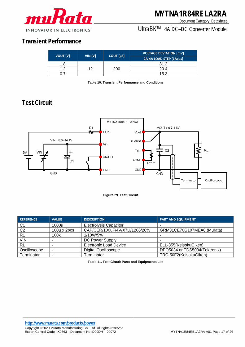
Transient Performance
Table 10. Transient Performance and Conditions
Test Circuit
Figure 29. Test Circuit
REFERENCE VALUE DESCRIPTION PART AND EQUIPMENT
C1 1000µ Electrolysis Capacitor - C2 100µ x 2pcs CAP/CER/100uF/4V/X7U/1206/20% GRM31CE70G107MEA8 (Murata) R1 100k 1/10W/5% - VIN - DC Power Supply - RL - Electronic Load Device ELL-355(KeisokuGiken) Oscilloscope - Digital Oscilloscope DPO5034 or TDS5034(Tektronix) Terminator - Terminator TRC-50F2(KeisokuGiken)
Table 11. Test Circuit Parts and Equipments List
VOUT [V] VIN [V] COUT [µF] VOLTAGE DEVIATION [mV] 2A-4A LOAD STEP (1A/µs)
1.8 12 200
31.2 1.2 20.4 0.7 15.3

MYTNA1R84RELA2RA Document Category: Datasheet
UltraBK™ 4A DC–DC Converter Module
http://www.murata.com/products/power Copyright ©2020 Murata Manufacturing Co., Ltd. All rights reserved. Export Control Code : X0863 Document No :D90DH – 00072
MYTNA1R84RELA2RA A01 Page 18 of 26
Component Selection Users of MYTNA1R84RELA2RA should adhere closely to the parts selected for the reference design bill of materials (BOM). Component selection is a complex process, and several parameters of importance to the design are not typically specified for passive components. Users wishing to deviate from these components are urged to contact Murata for guidance.
Input Fuse Certain applications and/or safety agencies may require fuses at the inputs of power conversion components. Normally, the fuse should be inserted on the primary side input supply line. For greatest safety, we recommend a fast blow fuse installed in the ungrounded input supply line of this module too. The installer must observe all relevant safety standards and regulations. For safety agency approvals, install the converter in compliance with the end-user safety standard.
Input Capacitor In general input environment (there are sufficient consideration about parasitic impedance and stability.), MYTNA1R84RELA2RA does not need an external input capacitor. If you want to reduce the ripple on input more, you can add the external input capacitor. The input capacitor should be placed as close to the module as possible to reduce any parasitic inductance effects. The voltage rating of the capacitor needs to be as high as the absolute maximum voltage rating for the system. The capacitor has voltage coefficient of capacitance, so you should be determine the rated value of capacitor that is taken into account the effective capacitance value at the applied VIN.
Output Capacitor We recommend a low-ESR ceramic (Murata GRM31 series) capacitor for output. The ceramic type capacitor may be tried using either single or multiple capacitors in parallel. The converter will achieve its rated output ripple and noise with additional external capacitor. The user may install more external output capacitance to reduce the ripple even further or for improved dynamic response. These capacitor should be placed as closely as possible to the converter, and the output ripple measured under your load conditions. Use only as much capacitance as required to achieve your ripple and noise objectives. Excessive capacitance can make step load recovery sluggish or possibly introduce instability or start-up failure. Do not exceed the maximum rated output capacitance listed in the specifications.

MYTNA1R84RELA2RA Document Category: Datasheet
UltraBK™ 4A DC–DC Converter Module
http://www.murata.com/products/power Copyright ©2020 Murata Manufacturing Co., Ltd. All rights reserved. Export Control Code : X0863 Document No :D90DH – 00072
MYTNA1R84RELA2RA A01 Page 19 of 26
Packaging Information This section provides packaging data including the moisture sensitivity level, package drawing, package marking and tape-and-reel information. Moisture Sensitivity Level The moisture sensitivity level rating for the MYTNA1R84RELA2RA in the 10.5 x 9.0 x 2.1mm LGA package is MSL3. Package Drawing
Figure 30. Package Outline Drawing
Recommended Board Land Pattern (Top View)
Figure 31. Recommended Board Land Pattern (Top View)

MYTNA1R84RELA2RA Document Category: Datasheet
UltraBK™ 4A DC–DC Converter Module
http://www.murata.com/products/power Copyright ©2020 Murata Manufacturing Co., Ltd. All rights reserved. Export Control Code : X0863 Document No :D90DH – 00072
MYTNA1R84RELA2RA A01 Page 20 of 26
Top Marking Specification
Figure 32. Top Marking Specification
Application Circuit
Figure 33. Application Schematic
Application Circuit Part List (Recommended)
REFERENCE VALUE DESCRIPTION PART NUMBER C1 1000u Electrolysis Capacitor (Optional)(1) - C2 100u x 2pcs CAP/CER/100µF/4V/X7U/1206/20% GRM31CE70G107MEA8 (Murata) Rtrim - Chip resistor/1/10W/0.5% RK73G1ETTP***D(KOA)
Table 12. Application Circuit Part List (1) If there is a non-negligible parasitic impedance between the power supply and the converter, such as during evaluation, the optional input capacitor "C1" may be required to reduce the impedance. The recommended optional capacitor is an example. Please consider the optimum value for the case. This capacitor is usually an aluminum electrolytic type. It isn't necessary to place the capacitor near the input terminal of the converter.
CODES DESCRIPTION
Pin 1 Marking
TNA1R84RELA2 Product code (Please see product code table beside)
Internal manufacturing code
PART NUMBER PRODUCT CODE MYTNA1R84RELA2RA TNA1R84RELA2

MYTNA1R84RELA2RA Document Category: Datasheet
UltraBK™ 4A DC–DC Converter Module
http://www.murata.com/products/power Copyright ©2020 Murata Manufacturing Co., Ltd. All rights reserved. Export Control Code : X0863 Document No :D90DH – 00072
MYTNA1R84RELA2RA A01 Page 21 of 26
Application Board Example
Figure 34. Applicatuin Board Example (Based on JEDEC standard)
114.5 × 101.5 × 1.6mm (4 Layer FR-4) Outside copper(1,4) layer=2oz, Inner copper(2,3) layer=1oz
Figure 35. Land Pattern Example

MYTNA1R84RELA2RA Document Category: Datasheet
UltraBK™ 4A DC–DC Converter Module
http://www.murata.com/products/power Copyright ©2020 Murata Manufacturing Co., Ltd. All rights reserved. Export Control Code : X0863 Document No :D90DH – 00072
MYTNA1R84RELA2RA A01 Page 22 of 26
Tape and Reel Specification Tape Dimension
Figure 36. Tape Dimension Reel Dimension
Figure 37. Reel Dimension
φ33
0±2
φ10
0±1
25.5±1.0
φ13.0±0.5φ21.0±0.8
Portion A
Indication
A
2.0±0.5

MYTNA1R84RELA2RA Document Category: Datasheet
UltraBK™ 4A DC–DC Converter Module
http://www.murata.com/products/power Copyright ©2020 Murata Manufacturing Co., Ltd. All rights reserved. Export Control Code : X0863 Document No :D90DH – 00072
MYTNA1R84RELA2RA A01 Page 23 of 26
Device orientation in Tape
Figure 38. Module Orientation in Tape Taping specification
Figure 39. Taping Specification
1. The adhesive strength of the protective tape is within 0.1-1.3N. 2. Each reel contains 400 or 100pcs. 3. Each reel set in moisture-proof packaging because of MSL 3. 4. No vacant pocket in “Module on tape” section. 5. The reel is labeled with Murata part number and quantity. 6. The color of reel is not specified.
MYTNA1R84RELA2RA Document Category: Datasheet
UltraBK™ 4A DC–DC Converter Module
http://www.murata.com/products/power Copyright ©2020 Murata Manufacturing Co., Ltd. All rights reserved. Export Control Code : X0863 Document No :D90DH – 00072
MYTNA1R84RELA2RA A01 Page 24 of 26
Order Codes
Table 13. Order Codes
Notices CAUTION
Limitation of Applications Please contact us before using our products for the applications listed below which require especially high reliability for the prevention of defects which might directly cause damage to the third party's life, body or property. ■ Aircraft equipment ■ Aerospace equipment ■ Undersea equipment ■ Power plant control equipment ■ Medical equipment ■ Transportation equipment (vehicles, trains, ships, etc.) ■ Traffic signal equipment ■ Disaster prevention / crime prevention equipment ■ Data-processing equipment ■ Application of similar complexity and/or reliability requirements to the applications listed in the
above
Note 1. Please make sure that your product has been evaluated in view of your specifications with our
product being mounted to your product. 2. You are requested not to use our product deviating from the reference specifications. 3. If you have any concerns about materials other than those listed in the RoHS directive, please
contact us. 4. Be sure to provide an appropriate fail-safe function on your product to prevent a second damage
that may be caused by the abnormal function or the failure of our product. 5. Please don’t wash this product under any conditions.
ORDER CODES DESCRIPTION PACKAGING SHIPPING METHOD
MYTNA1R84RELA2RA MYTNA1R84RELA2RA Buck Converter 10.5 x 9.0 x 2.1mm LGA 400 units/T&R
MYTNA1R84RELA2RAD MYTNA1R84RELA2RA Buck Converter 10.5 x 9.0 x 2.1mm LGA 100 units/T&R
MYTNA1R84RELA2RA Document Category: Datasheet
UltraBK™ 4A DC–DC Converter Module
http://www.murata.com/products/power Copyright ©2020 Murata Manufacturing Co., Ltd. All rights reserved. Export Control Code : X0863 Document No :D90DH – 00072
MYTNA1R84RELA2RA A01 Page 25 of 26
Product Specification Product Specification in this datasheet are as of August 2020. Specifications and features may change in any manner without notice. Please check with our sales representatives or product engineers.
Sales contact For additional information, contact Sales at https://www.murata.com/contactform.
Disclaimers The information described in this datasheet was carefully crafted for accuracy. However this product is based on the assumption that it will be used after thoroughly verifying and confirming the characteristics and system compatibility. Therefore, Murata is not responsible for any damages caused by errors in the description of the datasheet. Murata constantly strives improve the quality and reliability of our products, but it is inevitable that semiconductor products will fail with a certain probability. Therefore regardless of whether the use conditions are within the range of this datasheet, Murata is not responsible for any damage caused by the failure of this product.,(for example, secondary damage, compensation for accidents, punitive damage, loss of opportunity, and etc.) Also, regardless of whether Murata can foresee the events caused by the failure of our product, Murata has no obligations or responsibilities. The buyer of this product and developer of systems incorporating this product must analyze, evaluate, and make judgements at their own risk in designing applications using this product. The buyer and the developer are responsible for verifying the safety of this product and the applications, and complying with all applicable laws, regulations, and other requirements. Furthermore, the buyer and developer are responsible for predicting hazards and taking adequate safeguards against potential events at your own risk in order to prevent personal accidents, fire accidents, or other social damage. When using this product, perform thorough evaluation and verification of the safety design designed at your own risk for this product and the application. Murata assumes that the buyer and developer have the expertise to verify all necessary issues for proper use of the product as described above and to take corrective action. Therefore, Murata has no liability arising out of the use of the product. The buyer and developer should take all necessary evaluations, verifications, corrective actions and etc., in your own responsibility and judgment. This datasheet does not guarantee or grant any license to the information, including patents, copyrights, and other intellectual property rights, of the Murata or third parties. Regardless of whether the information described in this datasheet is express or implied, Murata does not take any responsibility or liability for any claims, damages, costs, losses, etc. Relating to intellectual property rights or other rights from third parties due to the use of these information.

MYTNA1R84RELA2RA Document Category: Datasheet
UltraBK™ 4A DC–DC Converter Module
http://www.murata.com/products/power Copyright ©2020 Murata Manufacturing Co., Ltd. All rights reserved. Export Control Code : X0863 Document No :D90DH – 00072
MYTNA1R84RELA2RA A01 Page 26 of 26
Patent Statement Murata products are protected to one or more of the U.S. patents.
Copyright and Trademark ©2020 Murata Manufacturing Co., Ltd. All rights reserved.
! This product is subject to the following operating requirements and the Life and Safety Critical Application Sales Policy. Refer to: https://www.murata.com/products/power/requirements
Murata Manufacturing Co., Ltd makes no representation that the use of its products in the circuits described herein, or the use of other technical information contained herein, will not infringe upon existing or future patent rights. The descriptions contained herein do not imply the granting of licenses to make, use, or sell equipment constructed in accordance therewith. Spec and cautions are subject to change without notice.