Embed Size (px)
Citation preview

Hardware and Software Design Methodologiesfor Portability, Flexibility and Versatility
in Multi-Standard MIMO Baseband Processing
Von der Fakultät für Elektrotechnik und Informationstechnikder Rheinisch–Westfälischen Technischen Hochschule Aachen
zur Erlangung des akademischen Gradeseines Doktors der Ingenieurwissenschaften
genehmigte Dissertation
vorgelegt vonDiplom–Ingenieur Daniel Günther
aus Neuss, Deutschland
Berichter: Universitätsprofessor Dr.-Ing. Gerd Ascheid
Universitätsprofessorin Cristina Silvano
Tag der mündlichen Prüfung: 10.07.2017
Diese Dissertation ist auf den Internetseitender Hochschulbibliothek online verfügbar.


Abstract
In modern wireless communications, the amount of communication standards thathave to be implemented by a communication device rises along with exponentiallyincreasing data rates. Therefore, the software-defined radio (SDR) concept envisionsa flexible, mostly programmable communication platform that can be adapted to newstandards by means of software updates. The conflict between flexibility and versa-tility on the one hand, and efficiency on the other hand is a significant challenge forthis approach. This is because flexibility and versatility often come at the expense ofincreased energy consumption and silicon area. Minimizing this trade-off is a centraltopic of this thesis. To this end, design paradigms for flexible programmable proces-sors and versatile non-programmable circuits, both with high efficiency, are developedand demonstrated by case studies. Another crucial aspect of SDR is ensuring softwareportability while maintaining high efficiency, since efficient software is often highlytailored to its target architecture. In response, this work presents concepts for the de-velopment of efficient portable baseband software, accompanied by implementationcase studies.
To investigate software portability, the receiver baseband signal processing of IEEE802.11n wireless LAN and the cellular LTE standard was implemented on two com-mercial SDR architectures. The target applications were analyzed on an algorithmiclevel and decomposed into their computationally complex kernels (Nuclei). For thesekernels, highly optimized, platform-specific implementations (Flavors) were devel-oped on both target architectures. The function interface of these Flavors on the otherhand remains generic, so that the target application can be composed by calls from aplatform-independent frame code that represents the control flow of the application.By doing so, a new communication standard can be implemented by adapting theframe code and potentially adding missing Flavors.
Application-specific instruction set processors (ASIPs) are often used to overcomethe efficiency-flexibility gap between specialized circuits and generic programmableprocessors. Typical baseband ASIPs commonly exhibit a high degree of complexity tocompete with tailored, non-programmable circuits which leads to poor flexibility andprogrammability. Therefore, this work pursues an alternative concept called the leandesign method. This method aims to identify the simplest architecture for a given

4
task and then make this architecture as efficient as possible. A slim and easily pro-grammable vector processor was developed as a case study to meet the requirementsof multi-antenna baseband processing. To improve ease-of-use and to avoid costlynumerical stabilization, the processor uses efficient floating-point arithmetic. A datapath with a flexible routing and permutation network and efficient bypassing ensureshigh utilization of the functional units. The data path can also be adapted to thenumerical requirements of the target application at runtime by masking the floating-point mantissa. The processor was layouted for a 90 nm CMOS technology to verifythe promised efficiency gain.
In case a flexible architecture does not provide sufficient performance for a certainapplication domain, the aspect of programmability often has to be given up. Lin-ear multi-antenna precoding based on singular value decomposition (SVD) for IEEE802.11ac with up to eight transmit antennas was selected as an exemplary use case forsuch a situation. A versatile precoding architecture has to support the maximum usecase as well as smaller antenna configurations. Therefore, the cyclic Jacobi algorithmfor SVD was adapted so it can decompose bigger size matrices entirely based on 2× 2vector arithmetic. Additionally, a number of numerical parameters can be adaptedto the requirements of the use case at hand. The resulting precoder was layoutedfor a 90 nm CMOS technology and benchmarked with respect to silicon area and en-ergy efficiency. Finally, the efficiency of the precoder was evaluated in the context ofa MAC layer application based on IEEE 802.11ac. The resulting multi-dimensionaldesign space includes antenna configurations, modulation schemes, etc., as well asseveral numerical parameters. Within this design space, the system was optimizedwith regard to different criteria (e.g., spectral efficiency, energy efficiency, latency).The versatility of the precoder architecture with respect to efficient support for theentire design space was instrumental to achieve the different optimization goals.

Kurzfassung
In der modernen, drahtlosen Kommunikationstechnik steigt mit wachsenden bereit-gestellten Datenraten gleichzeitig die Anzahl der umzusetzenden Kommunikations-standards. Das Software-Defined-Radio (SDR) Konzept sieht daher flexible, größten-teils programmierbare Kommunikationsplattformen vor, die durch Software-Updatesan neue Standards angepasst werden können. Eine Herausforderung ist dabei derKonflikt zwischen Flexibilität und Vielseitigkeit auf der einen Seite und Effizienz aufder anderen Seite, da Erstere oft gesteigerten Energieverbrauch und eine größere Si-liziumfläche bedeuten. Die Minimierung dieses Konflikts ist ein zentrales Themadieser Arbeit. Es werden Designparadigmen für effiziente, programmierbare Hard-ware sowie vielseitige Hardware ohne Programmierschnittstelle entwickelt und imRahmen von Fallstudien demonstriert. Eine weitere Herausforderung im Bereich SDRist die Portierbarkeit einer (Software-)Lösung bei gleichzeitigem Erhalt der Effizienz,da effiziente Software oft stark an ihre Zielarchitektur angepasst ist. Deshalb stelltdiese Arbeit Konzepte zur Entwicklung effizienter, portierbarer Basisband-Softwaremit entsprechenden Fallstudien vor.
Zur Untersuchung des Portierbarkeitsaspekts von SDR-Software wurde die Emp-fänger-Signalverarbeitung im Basisband für IEEE 802.11n WLAN und den zellulärenLTE-Standard auf zwei kommerziellen SDR-Architekturen implementiert. Die Zielap-plikationen wurden auf algorithmischem Level untersucht und in ihre recheninten-siven Kerne (Nuclei) zerlegt. Für diese wurden hochoptimierte Implementierungen(Flavors) auf beiden Zielarchitekturen entwickelt. Die Funktionsschnittstellen der Fla-vors sind jedoch generisch, so dass die Zielapplikation durch Aufrufe von Flavorsvon einem plattformunabhängigen Rahmencode zusammengesetzt werden kann, derden Kontrollfluss der Applikation widerspiegelt. Ein neuer Kommunikationsstan-dard kann nun durch Adaption des Rahmencodes und gegebenenfalls Hinzufügenzusätzlicher Flavors implementiert werden.
Zur Überwindung des zuvor erwähnten Effizienz-Flexibilitäts-Konflikts kommenoft Prozessoren mit anwendungsspezifischem Befehlssatz (application-specific instruc-tion set processors, ASIPs) zum Einsatz. Um mit spezialisierten, nicht programmier-baren Architekturen konkurrieren zu können, weisen gängige Basisband-ASIPs ofthohe Komplexität auf, was jedoch häufig zu verschlechterter Flexibilität und Pro-

6
grammierbarkeit führt. Daher wurde im Rahmen dieser Arbeit ein alternatives De-signkonzept (Lean Design Method) verfolgt, das eine möglichst einfache Architekturfür ein gegebenes Anwendungsfeld vorsieht und die resultierende, schlanke Hard-ware dann hochoptimiert. Als Fallstudie wurde für die Anforderungen der Sig-nalverarbeitung im Mehrantennen-Basisband eine schlanke, leicht programmierbareProzessorarchitektur entworfen. Zur verbesserten Programmierbarkeit und Vermei-dung aufwendiger numerischer Stabilisierung wird effiziente Fließkommaarithmetikverwendet. Ein Datenpfad mit einem flexiblen Routing- und Permutationsnetzwerksowie effizientem Bypassing ermöglicht eine hohe Ausnutzung aller Recheneinheiten.Auch kann der Datenpfad zur Laufzeit durch Maskierung der Fließkommamantissean die numerischen Anforderungen der Zielapplikation angepasst werden. Die Ef-fizienz der Architektur wurde anhand eines Layouts in 90-nm-CMOS bestätigt.
In Anwendungsfällen für die eine flexible Architektur nicht ausreichend perfor-mant ist, muss die Programmierbarkeit häufig aufgegeben werden. Mehrantennen-Präkodierung für IEEE 802.11ac mit bis zu acht Antennen wurde als Beispiel füreinen solchen Anwendungsfall ausgewählt. Eine vielseitige Präkodierungsarchitekturmuss diese maximale Anforderung genauso unterstützen wie kleinere Antennenkon-figurationen. Zu diesem Zweck wurde der zyklische Jacobi-Algorithmus zur Sin-gulärwertzerlegung adaptiert, so dass sich die Zerlegung größerer Matrizen auf 2× 2Vektorarithmetik abbilden lässt. Darüber hinaus lassen sich eine Reihe numerischerParameter an die Anforderungen des konkreten Anwendungsfalls anpassen. Fürden resultierenden Präkodierer wurde ein Layout in 90-nm-CMOS-Technologie er-stellt, und Benchmarks bezüglich Flächen- und Energieeffizienz wurden durchge-führt. Abschließend wurde die Effizienz des Präkodierers im Gesamtzusammen-hang einer MAC-Layer-Anwendung basierend auf IEEE 802.11ac evaluiert. Der re-sultierende mehrdimensionale Designraum umfasst Antennenkonfiguration, Modula-tionsverfahren, etc. sowie verschiedene numerische Parameter und wurde bezüglichunterschiedlicher Zielfunktionen (z.B. spektrale Effizienz, Energieeffizienz, Latenz)optimiert. Dabei stellte sich die Vielseitigkeit des Präkodierers als zentrales Werkzeugzum Erreichen der verschiedenen Optimierungsziele heraus.
Contents
1 Introduction 1
1.1 On Portability, Flexibility and Versatility . . . . . . . . . . . . . . . . . . . 2
1.2 Trends in Wireless Communications . . . . . . . . . . . . . . . . . . . . . 3
1.3 CMOS Technology Scaling . . . . . . . . . . . . . . . . . . . . . . . . . . . 6
1.4 Efficiency Metrics . . . . . . . . . . . . . . . . . . . . . . . . . . . . . . . . 9
1.5 Contributions . . . . . . . . . . . . . . . . . . . . . . . . . . . . . . . . . . 10
1.5.1 Numerically Aware Processing . . . . . . . . . . . . . . . . . . . . 10
1.5.2 The Lean Design Approach . . . . . . . . . . . . . . . . . . . . . . 11
1.5.3 System Level Study . . . . . . . . . . . . . . . . . . . . . . . . . . . 15
1.6 Outline . . . . . . . . . . . . . . . . . . . . . . . . . . . . . . . . . . . . . . 15
2 Selected Areas of MIMO Baseband Processing 17
2.1 Channel Model and Capacity . . . . . . . . . . . . . . . . . . . . . . . . . 17
2.1.1 Frequency-Flat Fading . . . . . . . . . . . . . . . . . . . . . . . . . 17
2.1.2 Spatial Multiplexing . . . . . . . . . . . . . . . . . . . . . . . . . . 19
2.1.3 Capacity Derivation for Slow Fading Channel . . . . . . . . . . . 19
2.2 Transceiver Overview . . . . . . . . . . . . . . . . . . . . . . . . . . . . . . 21
2.2.1 Acquisition of Channel State Information . . . . . . . . . . . . . . 21
2.2.2 Transmitter . . . . . . . . . . . . . . . . . . . . . . . . . . . . . . . . 22
2.2.3 Receiver . . . . . . . . . . . . . . . . . . . . . . . . . . . . . . . . . 23
2.3 Linear SVD Precoding . . . . . . . . . . . . . . . . . . . . . . . . . . . . . 23
2.3.1 Principle . . . . . . . . . . . . . . . . . . . . . . . . . . . . . . . . . 24
2.3.2 Precoding Gains . . . . . . . . . . . . . . . . . . . . . . . . . . . . . 25
2.4 MIMO Detection . . . . . . . . . . . . . . . . . . . . . . . . . . . . . . . . 26
i

ii CONTENTS
2.4.1 Optimal Detection . . . . . . . . . . . . . . . . . . . . . . . . . . . 27
2.4.2 Suboptimal Detection . . . . . . . . . . . . . . . . . . . . . . . . . 28
2.4.3 Comparison . . . . . . . . . . . . . . . . . . . . . . . . . . . . . . . 32
3 Multi-Platform, Multi-Standard Simulation Testbed 35
3.1 Evaluation of Communication Performance . . . . . . . . . . . . . . . . . 35
3.2 Exploration and Verification Flow . . . . . . . . . . . . . . . . . . . . . . 37
3.3 Modular Testbed . . . . . . . . . . . . . . . . . . . . . . . . . . . . . . . . 40
3.4 Integration of Demonstrator Platforms . . . . . . . . . . . . . . . . . . . . 40
4 The Nucleus Methodology: Application Analysis and Synthesis 43
4.1 Nucleus Analysis: Baseband Receiver for Wireless Communications . . 45
4.1.1 OFDM Modulation . . . . . . . . . . . . . . . . . . . . . . . . . . . 46
4.1.2 Channel Estimation . . . . . . . . . . . . . . . . . . . . . . . . . . . 47
4.1.3 Detection . . . . . . . . . . . . . . . . . . . . . . . . . . . . . . . . . 50
4.1.4 Permutation Based Tasks . . . . . . . . . . . . . . . . . . . . . . . 54
4.1.5 Channel Decoding . . . . . . . . . . . . . . . . . . . . . . . . . . . 55
4.1.6 Summary . . . . . . . . . . . . . . . . . . . . . . . . . . . . . . . . . 56
4.2 Target Platforms . . . . . . . . . . . . . . . . . . . . . . . . . . . . . . . . . 58
4.2.1 ST Microelectronics P2012 . . . . . . . . . . . . . . . . . . . . . . . 58
4.2.2 Texas Instruments TMS320C64x+ . . . . . . . . . . . . . . . . . . . 60
4.3 Algorithmic Design Space . . . . . . . . . . . . . . . . . . . . . . . . . . . 61
4.3.1 Equalizer . . . . . . . . . . . . . . . . . . . . . . . . . . . . . . . . . 62
4.3.2 Soft-Symbol Demapper . . . . . . . . . . . . . . . . . . . . . . . . 69
4.4 Application Synthesis . . . . . . . . . . . . . . . . . . . . . . . . . . . . . . 71
4.4.1 Adaptations for Narrow Wordwidth . . . . . . . . . . . . . . . . . 71
4.4.2 Flavor Implementation . . . . . . . . . . . . . . . . . . . . . . . . . 74
4.4.3 Application Benchmark . . . . . . . . . . . . . . . . . . . . . . . . 77
4.5 Discussion . . . . . . . . . . . . . . . . . . . . . . . . . . . . . . . . . . . . 81
5 napCore: An ASIP for MIMO Baseband Processing 83
5.1 Motivation . . . . . . . . . . . . . . . . . . . . . . . . . . . . . . . . . . . . 83
5.2 Architectural Design Space . . . . . . . . . . . . . . . . . . . . . . . . . . 85

CONTENTS iii
5.2.1 SIMD Architecture Type . . . . . . . . . . . . . . . . . . . . . . . . 85
5.2.2 IEEE 754 Floating-Point Compliance . . . . . . . . . . . . . . . . . 87
5.3 napCore Architecture . . . . . . . . . . . . . . . . . . . . . . . . . . . . . . 88
5.3.1 Pipeline Overview . . . . . . . . . . . . . . . . . . . . . . . . . . . 89
5.3.2 Operand Acquisition . . . . . . . . . . . . . . . . . . . . . . . . . . 90
5.3.3 Operand Bypassing . . . . . . . . . . . . . . . . . . . . . . . . . . . 91
5.3.4 Numerically Aware Processing . . . . . . . . . . . . . . . . . . . . 92
5.3.5 Floating-Point Newton-Raphson Iterator . . . . . . . . . . . . . . 92
5.3.6 Configurable Reduction Stages . . . . . . . . . . . . . . . . . . . . 93
5.4 Huawei Baseband DSP Architecture . . . . . . . . . . . . . . . . . . . . . 94
5.5 Synthesis Results . . . . . . . . . . . . . . . . . . . . . . . . . . . . . . . . 95
5.5.1 Design Space Exploration . . . . . . . . . . . . . . . . . . . . . . . 95
5.5.2 Energy Benchmark for Mantissa Masking . . . . . . . . . . . . . . 98
5.5.3 Comparison with Huawei Baseband DSP . . . . . . . . . . . . . . 98
5.6 Case Study: Equalizer-Based MIMO Detection . . . . . . . . . . . . . . . 100
5.6.1 Software Implementation . . . . . . . . . . . . . . . . . . . . . . . 100
5.6.2 Layout Implementation . . . . . . . . . . . . . . . . . . . . . . . . 103
5.6.3 Use Case Energy Assessment . . . . . . . . . . . . . . . . . . . . . 104
5.6.4 Comparison with State-of-the-Art . . . . . . . . . . . . . . . . . . 105
5.7 Discussion . . . . . . . . . . . . . . . . . . . . . . . . . . . . . . . . . . . . 109
6 napSVD: An ASIC for Linear MIMO Precoding 111
6.1 Motivation . . . . . . . . . . . . . . . . . . . . . . . . . . . . . . . . . . . . 112
6.1.1 Jacobi Based Implementations . . . . . . . . . . . . . . . . . . . . 112
6.1.2 Golub and Kahan Based Implementations . . . . . . . . . . . . . 112
6.1.3 The Need for a Versatile, High-Throughput Architecture . . . . . 113
6.2 2 x 2 SVD Algorithm and Architecture . . . . . . . . . . . . . . . . . . . . 113
6.2.1 CORDIC Algorithm . . . . . . . . . . . . . . . . . . . . . . . . . . 114
6.2.2 SVD Algorithm . . . . . . . . . . . . . . . . . . . . . . . . . . . . . 116
6.2.3 Architecture . . . . . . . . . . . . . . . . . . . . . . . . . . . . . . . 117
6.3 N x N SVD Algorithm and Architecture . . . . . . . . . . . . . . . . . . . 122
6.3.1 Algorithm . . . . . . . . . . . . . . . . . . . . . . . . . . . . . . . . 122

iv CONTENTS
6.3.2 Architecture . . . . . . . . . . . . . . . . . . . . . . . . . . . . . . . 125
6.4 Numerical Precision Analysis . . . . . . . . . . . . . . . . . . . . . . . . . 131
6.5 Implementation Results . . . . . . . . . . . . . . . . . . . . . . . . . . . . 133
6.5.1 Use Case Energy Benchmark . . . . . . . . . . . . . . . . . . . . . 135
6.5.2 Comparison with State-of-the-Art . . . . . . . . . . . . . . . . . . 136
6.6 Discussion . . . . . . . . . . . . . . . . . . . . . . . . . . . . . . . . . . . . 140
7 System Level Study of a Baseband Transmit System with SVD Precoding 143
7.1 Performance Metrics . . . . . . . . . . . . . . . . . . . . . . . . . . . . . . 143
7.2 Deployment Scenarios . . . . . . . . . . . . . . . . . . . . . . . . . . . . . 146
7.3 System Setup . . . . . . . . . . . . . . . . . . . . . . . . . . . . . . . . . . 147
7.3.1 Capacity of SVD Subsystem . . . . . . . . . . . . . . . . . . . . . . 147
7.3.2 Energy Breakdown . . . . . . . . . . . . . . . . . . . . . . . . . . . 150
7.3.3 Area Breakdown . . . . . . . . . . . . . . . . . . . . . . . . . . . . 153
7.4 Design Space . . . . . . . . . . . . . . . . . . . . . . . . . . . . . . . . . . . 155
7.4.1 Eigenmode Selection . . . . . . . . . . . . . . . . . . . . . . . . . . 156
7.4.2 Antenna Setup . . . . . . . . . . . . . . . . . . . . . . . . . . . . . 157
7.4.3 Adaptive Modulation and Coding . . . . . . . . . . . . . . . . . . 158
7.5 Methodology . . . . . . . . . . . . . . . . . . . . . . . . . . . . . . . . . . . 159
7.6 Multidimensional Design Space Exploration . . . . . . . . . . . . . . . . 160
7.6.1 Spectral Efficiency, Energy Efficiency & Power Consumption . . 161
7.6.2 Latency . . . . . . . . . . . . . . . . . . . . . . . . . . . . . . . . . . 169
7.7 Discussion . . . . . . . . . . . . . . . . . . . . . . . . . . . . . . . . . . . . 173
8 Conclusions and Outlook 177
8.1 Summary . . . . . . . . . . . . . . . . . . . . . . . . . . . . . . . . . . . . . 178
8.2 Discussion . . . . . . . . . . . . . . . . . . . . . . . . . . . . . . . . . . . . 181
8.3 Outlook . . . . . . . . . . . . . . . . . . . . . . . . . . . . . . . . . . . . . . 183
Appendix 185
A Derivations 185
A.1 Computational Complexity of Triangular Matrix Inversion . . . . . . . . 185
A.2 Computational Complexity of Selected Matrix Factorizations . . . . . . 186

CONTENTS v
A.2.1 LU Factorization . . . . . . . . . . . . . . . . . . . . . . . . . . . . 186
A.2.2 LDLh Factorization . . . . . . . . . . . . . . . . . . . . . . . . . . . 186
A.2.3 Modified Gram-Schmidt QR Factorization . . . . . . . . . . . . . 187
Glossary 189
Bibliography 197
Publication List 209
Curriculum Vitae 211

vi CONTENTS

Chapter 1
Introduction
With modern life becoming more and more complex, society’s need for more pow-erful, flexible and versatile tools is growing accordingly. This trend is particularlystrong in the domain of integrated circuits and their use in everyday life. The ad-vent of the smartphone, for example, has made voice and data communication andmultimedia technology widely available to the consumer market. A key factor to thesuccess of the smartphone is its versatility. The device can connect to virtually anycivil communication network, whether it is a wireless local area network (LAN), acellular network, or an ad-hoc mesh. At the same time, a programmable applicationplatform making use of the phone’s communication capabilities can provide variousservices at any location where adequate connectivity is provided.
The story of the smartphone is just one example of a general trend. More andmore functionality is expected from a single integrated circuit. As a result, thereis a shift from tailored circuits for one specific task to more generic circuits thatsolve a multitude of problems. One prominent example from the communicationsdomain is software radio (SR) [19]. Instead of integrating one dedicated circuit foreach communication standard, an SR contains flexible, programmable hardware thatcan support multiple standards in software. The only analog components in an SRare the analog-to-digital and digital-to-analog converters (ADC/DAC) and the connectedantenna subsystem. All remaining functionality is realized purely in software. Theconcept of software-defined radio (SDR) relaxes the demand for a pure software solu-tion [114]. SDR uses hardware accelerators for tasks where available programmablearchitectures cannot provide sufficient throughput under the given constraints (e.g.,energy budget or heat dissipation).
While a (mostly) programmable SDR is highly flexible, this flexibility is penalizedby a reduced efficiency in terms of silicon area and energy consumption. This trade-off is commonly referred to as the efficiency-flexibility gap, pointing at the fact thatan architecture with emphasis on flexibility will exhibit drawbacks in efficiency andvice versa. A common strategy to improve the efficiency of SDRs is to reduce theirflexibility “just enough” so that their efficiency is sufficient for the target applicationdomain. In case energy consumption is not critical, digital signal processors (DSPs)are an attractive option, since they are tailored to signal processing but no specificapplication in particular. When the constraints on efficiency are stricter, the genericnature of the target architecture has to be restricted. An application-specific instruction-set processor (ASIP) is tailored to a specific application domain but still retains a certainflexibility. When throughput requirements or constraints on efficiency also render anASIP solution unsuitable, the programmability of the architecture has to be given up
1

2 Chapter 1. Introduction
entirely. The resulting architecture is an application-specific integrated circuit (ASIC) thathas no programming interface and is highly tailored to one specific application.
Hardware developers of, or software developers for flexible architectures naturallytry to narrow the efficiency-flexibility gap as much as possible. A common approachin hardware design is the development of increasingly complex architectures with de-creasing usability and programmability. The corresponding trend in software designresults in highly convoluted software which is strongly tailored to the target architec-ture and therefore hard to adapt or to port to another architecture. This work takes theopposite approach to the aforementioned trends. Instead of developing increasinglycomplex solutions, the paradigm to “make the simplest solution as efficient as possible”is proposed. This principle is also referred to as the lean approach. It is the goal ofthis thesis to show the applicability of this principle to the design of embedded soft-ware, flexible ASIPs, and versatile ASICs that are able to support a wide range of usecases. At the same time, the concept of numerically aware processing (NAP) ensuresthat the aforementioned solutions can adapt to the numerical requirement of each usecase. Multiple-input and multiple-output (MIMO) baseband processing serves as acase study to demonstrate the feasibility of these two core concepts.
1.1 On Portability, Flexibility and Versatility
As motivated by the previous section, portability, flexibility and versatility are desir-able qualities for processing systems, regardless of whether they are implemented insoftware, hardware, or a mix of both. So far, the terms portability, flexibility and ver-satility have been used according to their intuitive meaning, but in the scope of thisthesis, it is important to define and distinguish them clearly.
• Portability denotes how “easy” it is to port an existing implementation of anapplication from one target architecture to another. The exact nature of the im-plementation is not fixed in this context. It may be a piece of software writtenin a high-level programming language, optimized assembly code, or a hard-ware description language (HDL) based representation that gets mapped onto afield-programmable gate array (FPGA). The authors of [125] suggest to quantifyportability as the reciprocal of the effort (e.g., man-months) of porting the exist-ing application to a new architecture. Naturally, this metric is only suitable asa guidance, since the exact number depends on factors like skill and experienceof the person who performs the porting.
• Flexibility indicates how easily a new application can be implemented on a cer-tain architecture or architecture class. The authors of [11] propose the definitionof flexibility as the reciprocal of the implementation time of the application. Incomparison to the aforementioned portability metric, the implementation pro-cess is not aided by any previous implementation that can be adapted to the newtarget architecture. Results differ depending on whether architecture classes orspecific architectures are discussed. ASICs as an architecture class, for example,
1.2. Trends in Wireless Communications 3
are regarded less flexible than ASIPs, as the implementation of a specific tasktakes less time for an ASIP solution, particularly due to the programmability ofthe ASIP. When considering specific ASIC architectures, as done in this work,most of them have to be considered as not flexible at all, since they are incapableof performing tasks that they were not designed for.
• Versatility expresses the fitness of an implementation to process multiple vari-ants of a certain application. In contrast to flexibility or portability, this metricis not based on the implementation process of new applications but evaluatesthe properties of an already existing one. Even if a piece of software or hard-ware is not flexible in the strict sense of the above definition (e.g., it provides noprogramming interface), it can still be versatile in the scope of its target appli-cation or application domain. ASIC design for multi-standard, multi use casewireless communication is a prime example where this is desirable. For MIMOprecoding or complex MIMO detection algorithms, throughput requirements ofmodern communication standards and energy constraints of battery-powereddevices may demand an ASIC implementation. Still, this ASIC should not beconstrained to one specific use case (e.g., constellation alphabet, code rate, an-tenna setup) but be capable to process all of them. Therefore, the ability to servemultiple variants of one specific application is referred to as versatility in thescope of this work.
Within this thesis, three implementations from the domain of MIMO basebandprocessing are presented, each of them putting their focus on a different subset of thethree metrics above. The physical (PHY) layer inner modem software implementationin Chapter 4 is designed for portability, using a design methodology that fosters rapiddevelopment and thus flexibility. The ASIP from Chapter 5 aims at high flexibility byproviding a slim but highly optimized architecture with a comprehensible program-ming interface. Chapter 6 shows MIMO precoding as a demanding application do-main that requires an optimized ASIC implementation. However, the algorithm andarchitecture design delivers a versatile implementation suitable for a multitude of usecases.
1.2 Trends in Wireless Communications
Data rates in consumer communication technology have undergone a massive growthin the last two decades. This development has been formalized by Edholm’s law [27],stating that the data rates of the three major types of communication technologiesdevelop exponentially over time, each at its own growth rate. In this context, typesof communication technology are separated by their mobility (i.e., the ability of theuser to move around freely). Wireless, nomadic, and wireline denote cellular systemswith high mobility, wireless LANs with medium mobility (i.e., restricted to a specificarea), and wired communication (e.g., via Ethernet) without any mobility, respec-tively. Figure 1.1 gives an overview of the theoretical peak data rates achievable by

4 Chapter 1. Introduction
1994 1996 1998 2000 2002 2004 2006 2008 2010 2012 2014 2016104
105
106
107
108
109
1010
1011
1012
802.11
802.11b
802.11g
802.11n
802.11ac
GPRSUMTS-R99 EDGE
HSDPA-R5HSDPA-R7
HSDPA-R9
HSDPA-R11LTE-R8
LTE-R10 LTE-R12802.3ab
802.3an
802.3ba
year
data
rate
[bit
/s]
nomadic (WLAN)wireless (cellular)wireline (LAN)
Figure 1.1: Data rate development in nomadic, wireless and wireline communica-tion.
a selected set of relevant standards as a function of the year their respective stan-dardization was finished. The interpolated annual growth rates are 1.5 for wireline,1.6 for wireless LAN, and 1.8 for cellular communication. Therefore, the gap in datarate between wireless LAN and cellular communication has narrowed notably in re-cent years, and it is foreseeable that their data rates will converge at some point [27].This assumption is reasonable from a PHY layer perspective since recent versions ofboth technologies (i.e., LTE [38] and IEEE 802.11ac [72]) employ similar techniqueslike MIMO transmission and orthogonal frequency-division multiplexing. However,it must be kept in mind that the listed data rates are peak values for ideal conditions.Particularly for cellular communication, only a fraction of these rates will be achievedin crowded cells or at high relative transmitter-receiver velocity.
The exponential growth of data rates present a serious challenge for the silicontechnology that has to implement these standards. Moore’s law [87] predicts an ex-ponential growth of the number of components that can be integrated on a singlechip for the minimum price point and puts the growth rate in the same range asthe increase in data rates mentioned above. However, the rate of further integrationis starting to decline in recent years, particularly due to increased costs in fabrica-tion [88]. Additionally, an increase in available silicon complexity by a certain factordoes not guarantee an equal increase in data rate. For MIMO transmission schemes

1.2. Trends in Wireless Communications 5
that exploit spatial diversity (see Chapter 2), computational complexity often exhibitsa polynomial or exponential dependency on the number of antennas, which meansthat the energy consumption per unit of transmitted information increases. Espe-cially for battery-powered devices, this increase is critical and it significantly shortensbattery life.
Increasing the number of transmit and receive antennas to exploit spatial diver-sity is only one (costly) option to increase data rates which partly owes its popularityto the scarcity of available spectrum. Without this limitation, the most efficient wayto scale data rates is to increase the transmission bandwidth. For this reason, newstandards try to use less populated parts of the spectrum and assign more bandwidthto a single channel. The recent IEEE 802.11ac [72] standard, for example, moved awayfrom the overcrowded 2.4 GHz band and operates exclusively at 5 GHz, where a sin-gle channel can be assigned up to 160 MHz of bandwidth. In comparison, the priorIEEE 802.11n [69] standard only allocates up to 40 MHz to one channel. The IEEE802.11ad [70] standard goes even further and gives up the spatial diversity aspectwhilst assigning 1760 MHz to a single channel in the 60 GHz spectrum. The draw-back of transmission at such high frequencies is the high absorption of radio wavesby the air which limits the range of commercial applications to around 10 m and gen-erally does not allow transmission through walls [56], for example. Therefore, it ismost suitable for high data rate, short range communication like the transmission ofuncoded high resolution video [115]. Another approach to increase data rates is topack more bits into a symbol that is then transmitted via the wireless channel. Thistrend is also visible in recent communication standards. In 802.11n [69] wireless LAN,the densest constellation alphabet contains six bits per symbol. For 802.11ac [72], thisnumber has been increased to eight bits per symbol, and the latest draft of the upcom-ing IEEE 802.11ax [73] standard even plans to use ten bits per symbol. Once again,delivering the data rates promised by such use cases demands either very good chan-nel conditions or additional processing power (see Chapter 2).
In conclusion, it is becoming increasingly difficult to realize higher data rateswith current silicon technologies, in particular when limited by the capacity of avail-able batteries. The previous considerations make it clear that this challenge can notbe met by increasing degrees of circuit integration alone. Instead, conceptual researchon the architectural and algorithmic level is required. Recent algorithmic works haveaimed at creating suboptimal MIMO baseband algorithms that offer a substantial re-duction of computational complexity whilst minimizing the penalty in terms of com-munication performance (see Section 2.4.2, for example). This concept can be drivenfurther by the turbo principle [58] where components of the baseband receiver itera-tively exchange information and thereby improve the overall communication perfor-mance. The turbo principle allows the use of low-complexity, suboptimal algorithmswhile achieving close to optimal performance. Its potential for practical implementa-tions has been demonstrated in VLSI research (e.g., iterative detection and decodingin [13]). Another approach to cope with increasing complexity is NAP, which playsa key role in this work. The idea of NAP is related to the concept of approximatecomputing [59] which has been studied in the field of image/video processing. Ap-

6 Chapter 1. Introduction
proximate computing assumes that a small degradation of processing accuracy istolerable due to perceptual limitations of humans with regard to multimedia content.NAP adapts numerical parameters (e.g., wordwidth, number of iterations, etc.) tothe requirements of the current use case. There are several goals according to whichthese requirements can be defined. A straightforward approach is to assign as muchprecision as required for a numerically stable execution. This could mean, for exam-ple, that a specific wordwidth that delivers the same communication performance asa double precision floating-point reference implementation is chosen. However, theconcept of NAP also extends to the trading of numerical precision for energy effi-ciency. For some use cases, this is can be particularly attractive (see Chapter 7), as theloss of communication performance is hardly observable while the impact on energyefficiency is highly noticeable.
1.3 CMOS Technology Scaling
Moore’s law [87], published in 1965, predicts that the number of components that canbe integrated on a chip for the minimum price point doubles approximately each year.Continuous advances in the down-scaling of complementary metal-oxide-semiconductor(CMOS) circuits based on metal-oxide-semiconductor field-effect transistors (MOSFETs)[61] are a main driver of this trend. The following section gives a brief overview ofthe functionality of a MOSFET, as well as technology scaling and its limits.
The basic structure of an n-channel MOSFET is depicted in Figure 1.2. The tran-sistor body is made up of semiconductor material (e.g., silicon) with free positivecharges (p-type). The source and drain terminals are established by doping with el-ements that provide free negative charges (n-doped). The gate terminal is separatedfrom the body by an insulation material (e.g., silicon oxide) of thickness tox. Applyinga positive voltage VGS between gate and source creates an electric field that attractsnegative minority charges in the body material. When VGS crosses the threshold volt-age VT, a conducting channel of length L and width W composed of negative chargesis formed under the gate oxide (hence the name n-channel MOSFET).
For the relevant considerations at this point, a MOSFET can be seen as a threeterminal device1. For typical CMOS logic that operates in the saturation domain [94],a MOSFET can be modeled as a switch, where the voltage VGS controls whether ornot the connection between drain and source is closed or open. When a voltage at thelevel of the supply voltage Vdd is applied to VGS, the switch is considered closed. Theresulting current delivered at the drain terminal is [94]
ID = vn(x)Qi(x)W (1.1)
for charge density Qi and charge velocity vn at position x between source and drain.Ideally, a charge traveling through the channel between source and drain would getaccelerated according to the electric field caused by voltage VDS between drain and1 The body terminal is supposed to be connected to ground or Vdd for n-channel and p-channel
MOSFETs, respectively.

1.3. CMOS Technology Scaling 7
L
tox
source draingate
body
W
n-dopedn-doped
p-substrate
gate oxide
Figure 1.2: N-channel MOSFET schematic.
source. However, increasing degrees of integration mean shrinking channel lengths L(short channel) and therefore rising electric fields EDS = VDS/L. For channel lengths inthe range of nanometers, the resulting electrical field is so high that scattering effectsbecome the limiting factor of charge transport, constraining vn to the saturation veloc-ity vsat independent of voltage VDS [94]. This is a significant drawback for technologyscaling since it limits the drain current to
ID = vsatQiW. (1.2)
In the context of this work, technology scaling refers to shrinking the feature size(i.e., L, W, tox) by a factor 1/S and reducing the voltage levels by a factor 1/U. Thefollowing gives a brief overview of the impact of these scaling factors on power P,energy E, and clock frequency fclk. From (1.2), it follows [94] that
ID ≈ vsatεox
toxW (VGS −VT) ∝ 1/U (1.3)
for permittivity εox of the gate oxide material. As a result, the power of the transistorapproximately satisfies
P ≈ vsatεox
toxW (VGS −VT)VDS ∝ 1/U2. (1.4)
This finding has a significant impact on scaling. Since tox and W both shrink by 1/S,scaling effects of feature size on power cancel each other out, and only the dependencyon the voltage levels remains. The achievable clock frequency is inversely proportionalto the propagation delay tp, the time it takes to charge the gate terminal of a MOSFET.Approximating the transistor gate as a rectangular capacitor with capacity [61]
CG = εoxWLtox
, (1.5)
it follows thattp ∝ CG
Vdd
ID= εox
WLtox
Vdd
ID. (1.6)

8 Chapter 1. Introduction
Property Symbol Scaling factor
Channel geometry W, L, tox 1/SSupply voltage Vdd 1/UDevice area A 1/S2
Drain current ID 1/UClock frequency fclk SPower P 1/U2
Energy E 1/(SU2)
Table 1.1: Scaling of short channel MOSFET properties by voltage scaling factor Uand feature size scaling factor S.
Since any effects of S or U cancel out from the fraction Vdd/ID, the impact of technol-ogy scaling on the clock frequency is given by
fclk ∝tox
WL∝ S. (1.7)
The impact of scaling factors S and U on a MOSFET is summarized in Table 1.1.Based on this table, the performance parameters of a design implemented in one tech-nology can be estimated for the use of another technology with different feature sizeand voltage levels. However, these scaling mechanisms can only be used as a roughestimate since they are derived for a single transistor (i.e., the influence of intercon-nects is not considered). Moreover, scaling is specific to details of the semiconductortechnology. Changing the isolation material under the gate terminal, for example, willimpact the capacitance in (1.5) via εox which is not considered in geometry or voltagescaling.
When developing new silicon technology nodes, there are different ways in whichthe scaling factors from Table 1.1 can be used. Full scaling [94] sizes down feature sizeand voltage levels by the same factor, meaning area and power shrink quadraticallywhile the clock frequency rises linearly with this factor. Full scaling is the ideal sce-nario for the development of a new technology node since it exploits the full potentialof scaling to size-down and speed-up silicon technology while improving power con-sumption and energy efficiency. However, recent technology nodes have been unableto exploit full scaling with respect to voltage factor U [116]. This is partly due to theindustry’s desire to maintain compatibility with existing logic voltage levels [94] andpartly to limit leakage current (i.e., current flowing despite the MOSFET switch beingin its open state) [30]. As a result, voltage has remained almost constant (constantvoltage scaling) in recent technology nodes [37]. This is problematic from a thermalperspective, since the power per transistor remains the same (see Table 1.1) whiletransistor size shrinks. This, in turn, means that the power dissipation per unit of

1.4. Efficiency Metrics 9
chip area increases proportionally to S2. At one point, the generated heat cannot beremoved anymore and the integrity of the device is compromised. Therefore, thetheoretical integration capability provided by new technology nodes cannot be fullyutilized anymore, an effect that has been dubbed dark silicon [37]. One practical impli-cation of dark silicon is that on a densely integrated chip, not all components can beactive at the same time or run at full utilization. This finding underlines the impor-tance of NAP. Depending on the thermal conditions on the chip, it may be necessaryto alter certain numerical parameters to reduce heat dissipation so the chip remainsfunctional but delivers a slightly degraded communication performance.
1.4 Efficiency Metrics
The previous sections already mentioned that the efficiency of an implementationcan be judged based on how much hardware resources and energy it consumes fora certain task. In the following, this notion is specified further by the definition ofthree different types of efficiencies that are used throughout this thesis to evaluate theperformance of different baseband processing solutions.
• Hardware efficiency ηH denotes the information throughput Θ in bits per sec-ond normalized to a technology independent metric for hardware complexity.Within the scope of this work, hardware complexity is defined as the size AGEof the post-synthesis standard cell area in gate equivalents (GE), where one gateequivalent corresponds to the size of a single two-input NAND-gate with afanout of one for the respective technology [78]. Therefore, hardware efficiencyis given by
ηH =Θ
AGE[bit/s/GE]. (1.8)
• Area efficiency ηA is given by the information throughput Θ normalized to theoccupied silicon area A, typically in square millimeters, for a specific technology.Therefore, area efficiency only allows comparison with other architectures de-signed for the same technology. Otherwise, results have to be scaled (see Section1.3). In contrast to hardware efficiency, area efficiency also allows a quantifica-tion of those elements on a chip that cannot be expressed in gate equivalents(e.g., analog components). A common example thereof are static RAMs thatcontain analog sense-amplifiers [78].
ηA =ΘA
[bit/s/mm2] (1.9)
• Energy efficiency ηE is defined as the information throughput Θ normalized tothe power consumption P of the hardware implementation. This corresponds tothe amount of processed information per unit of energy.
ηE =ΘP
[bit/J] (1.10)
10 Chapter 1. Introduction
Just like area efficiency, energy efficiency depends on the target technology andhas to be scaled when compared to architectures designed for other technolo-gies.
1.5 Contributions
The following section highlights the contributions of this work to enable portability,flexibility and versatility of hardware and software solutions for MIMO basebandprocessing while maintaining competitive efficiency. NAP (see Section 1.5.1) and thelean design approach (see Section 1.5.2) are the main two design methods employedthroughout this work. They are applied to a pure software design, a flexible ASIPand a versatile ASIC. The impact of these two methods is studied individually forthe aforementioned implementations as well as from a system level perspective (seeSection 1.5.3).
1.5.1 Numerically Aware Processing
NAP is a core concept that is applied to all implementations presented in this work.Within the context of this thesis, NAP refers to the notion of signal processing imple-mentations that can adapt their numerical precision at runtime (e.g., in response tochanging outer constraints). The way in which numerical precision is adapted variesaccording to the nature of the signal processing application and its target architecture.
1. Standard digital signal processors: Off-the-shelf DSP platforms (e.g., Texas In-struments (TI) C64x+ [106]) typically do not offer capabilities to adapt numericalprecision explicitly by techniques like mantissa masking (see Chapter 5). Mim-icking such capabilities purely in software is too costly in terms of executiontime and the overhead would nullify the potential gains of precision adapta-tion. Instead, the software developer has to accept the number format (e.g.,fixed-point or floating-point with a certain number of bits) as fixed and ratherchoose suitable algorithms for each specific use case. This means, for example,choosing more stable algorithms for more numerically challenging tasks likeMIMO detection for a denser constellation or a higher order antenna setup. Forless numerically demanding use cases on the other hand, less stable but poten-tially faster algorithms may be used. The software implementations presentedin Chapter 4 give an overview of how algorithms are adapted according to nu-merical precision requirements.
2. ASIPs: During the design of a programmable architecture, hardware measuresthat enable NAP can be included and exposed directly to the programminginterface. The ASIP architecture presented in Chapter 5, for example, providesa floating-point data path where the wordwidth of each floating-point wordcan be adapted by a bitmask applied to a number of LSBs of the floating-pointmantissa. Further adaptations can be made on an algorithmic level (e.g., numberof iterations for iterative algorithms).

1.5. Contributions 11
3. ASICs: Since it is specifically tailored to one application, an ASIC design hasthe potential to deliver a wider set of numerical precision adaptation methodsthan a DSP or an ASIP. The versatile ASIC for singular value decomposition (SVD)presented in Chapter 6 allows the adaptation of the number of iterations of thedecomposition algorithm, the number of CORDIC iterations for trigonometricoperations, and several bitmasks to reduce the wordwidth within the data path.These three measures combined promise a high scalability of power and energyconsumption.
The purpose of the application of NAP may also vary depending on the exactapplication scenario. One aspect is the variance of numerical precision requirementsdepending on the use case, meaning in order not to waste energy, the applicationshould always run with the minimum precision required by each particular scenario.Another prospect is to trade-off numerical precision and hence communication per-formance against low execution time, energy efficiency, or operational constraints.For mobile, battery-powered devices, energy efficiency is of utmost importance. Sit-uations may arise where keeping a link alive for a longer time is worth a marginalreduction in communication performance. But also communication equipment withconstant power supply (e.g., base stations, wireless LAN access points) may stronglybenefit from this trade-off, since components are often passively cooled and have tooperate within certain thermal constraints which become more and more critical withthe increasing density of transistors integrated on a chip (see Section 1.3). Keepingthe overall equipment operational can be considered more valuable than achievingmaximum communication performance for each client/subscriber while risking theintegrity of the entire device.
1.5.2 The Lean Design Approach
Along with NAP, the lean design approach is a central design paradigm for all im-plementations in this work. The lean design approach results from the observationthat with increasing application complexity, it is often the case that the complexityand the degree of specialization of the resulting hardware and software implementa-tions rise equally. Wireless communication with exponentially growing data rates (seeSection 1.2) is a prime example of this trend. Increasing complexity and specializationare critical for the application domain of modern wireless communications becausea device has to support a wide spectrum of communication standards and not justthe most recent one. This motivates the development of software solutions, as wellas flexible and versatile hardware. At the same time, tight energy budgets and ther-mal constraints put pressure on such implementations to be as efficient as possible.In many cases, this results in a number of undesirable consequences as the under-lying design philosophy often seems to be that complex problems require complexsolutions. The lean design approach takes the opposite stance, stating that to solvecomplex problems, one should aim for simple solutions to make the high degree ofcomplexity manageable. The following describes undesirable trends in wireless com-

12 Chapter 1. Introduction
munication solutions and how these trends can be counteracted by the lean designapproach to software and hardware development.
1.5.2.1 Software Design
MIMO baseband processing has tight real-time requirements that impose a challengeon a pure software implementation, particularly for higher order MIMO transmissionschemes as in IEEE 802.11n/ac [69, 72]. As a result, the software implementation ofeach standard has to be highly optimized and tailored to the target platform. Thisneed for optimization counteracts a number of other goals of software design.
1. Readability & adaptability: Software should be comprehensible so that its func-tionality is clearly accessible for new developers and can be adapted easily.Highly optimized, convoluted code on the other hand tends to obscure high-level functionality and makes it harder for developers to adapt or modify thesoftware.
2. Minimize time to market: Software solutions have the advantage that they canbe implemented and verified with minor time effort compared to hardware-software co-designs or tailored ASICs. If, however, a software has to be exces-sively optimized for the target platform, the advantage in time to market of apure software solution is diminished.
3. Portability: Software programmed in standardized programming languageslike ANSI C can be ported to any platform for which a matching compiler exists.The optimization of software for low execution time, on the other hand, typi-cally requires the use of non-standardized, platform-specific extensions to theprogramming language. These intrinsics allow the programmer to access specialcapabilities of the target architecture (e.g., for vector arithmetic). While enablinga significant speed-up of the execution, the resulting implementations are notportable to other platforms.
The Nucleus methodology is a concept for application analysis, synthesis, and map-ping onto potentially heterogeneous platforms, which makes it particularly suitablefor SDR solutions. With its analytic approach, it fosters slim, efficient software im-plementations as envisioned by the lean design method and mitigates the aforemen-tioned drawbacks of platform-specific software optimization. The starting point of theNucleus methodology is the analysis of the target application domain and the identi-fication of computationally complex, execution time intensive kernels which are alsoreferred to as Nuclei. Each Nucleus is a purely algorithmic construct, independent ofany practical implementation. Exemplary Nuclei from the domain of MIMO basebandprocessing are Fourier transformation, matrix inversion, and further vector arithmeticoperations. Based on this analysis, the target applications can be described entirelybased on a number of Nuclei embedded into a control flow. The control flow itself canbe described by a data-flow graph (e.g., a Kahn process network [79]) or by genericframe code written in the target programming language. Here, frame code means

1.5. Contributions 13
platform-independent code that calls the functions corresponding to the respectiveNuclei. Highly optimized implementations of the identified Nuclei called Flavors arebundled in the Flavor library. The Flavor library is highly platform-dependent and hasto be re-implemented for each target platform. However, research conducted withinthe scope of this work [52] has shown that typical baseband applications can be com-posed out of a small set of Nuclei, whose Flavors are called multiple times from theframe code.
The Nucleus methodology counteracts the previously mentioned drawbacks ofplatform-specific software development. Due to the strict separation of control flowand computational payload, the code becomes comprehensible and thus easily ex-tendible. Since only a few Flavors have to be implemented per platform, rapid devel-opment (e.g., of new communication standards) is enabled. Also, portability betweenplatforms is improved, since only the Flavor library has to be ported. A detaileddemonstration of the aforementioned software design principle is presented in Chap-ter 4.
1.5.2.2 Towards Flexible, Efficient ASIPs
To compete with tailored ASIC designs in the domain of MIMO baseband process-ing (e.g., sphere detector [124] and MMSE-PIC [103]), designers of flexible circuitshave developed increasingly complex architectures. The reconfigurable ASIP (rASIP)design concept [26], for example, extends an ASIP core by attaching a coarse-grained,reconfigurable array (CGRA) of connected processing elements with scalar arithmeticcapabilities. While the ASIP is programmable in assembly, the CGRA has to be config-ured via a bitstream, which reduces the ease of programming. This becomes more andmore problematic if the complexity of the processing elements or the CGRA connec-tion infrastructure increases. The aforementioned architecture points to the potentialproblems when trying to compete with tailored ASICs by developing increasinglycomplex ASIPs.
1. Optimization focus: A more complex design naturally results in more circuitrythat has to be optimized. Instead of focusing on a few essential aspects, opti-mization has to cover a wide set of hardware elements. This lack of focus islikely to result in inefficiencies.
2. Ease-of-use: The original incentive of ASIP design is to provide a flexible, pro-grammable alternative to tailored ASICs. In competitive setups where time tomarket is key, flexibility does not only mean being able to implement a varietyof applications on a platform, but rather enabling rapid development of theseapplications (see Section 1.1). Thus, ease-of-use is paramount for a truly flexiblearchitecture.
These findings motivate the application of the lean approach to ASIP design. Dueto its popularity in the open literature, MIMO detection is selected as a case studyand the results are presented in Chapter 5. In the domain of MIMO detection, many

14 Chapter 1. Introduction
algorithms rely on complex-valued vector arithmetic (see Section 2.4.2). Therefore, avector processor, also referred to as a single instruction, multiple data (SIMD) proces-sor, is selected as the target architecture type. All implementation effort can now befocused on optimizing the slim architecture (e.g., to ensure high utilization of all func-tional units). To enable flexibility in the sense of rapid development [12], the numberformat of the architecture is a critical factor. Research in the scope of this work hasshown that a major share of the implementation effort for MIMO baseband applica-tions is spent on numerical stabilization of fixed-point algorithms [51]. This effortcan be minimized by shifting parts of the stabilization from the software to the hard-ware domain, which can be realized by using the inherently stabilized floating-pointnumber format.
1.5.2.3 Towards Versatile ASICs
Tailored ASIC solutions are typically perceived as the counter-pole of flexible, versa-tile designs. While this may be the case for many ASIC implementations, it is rathera design flaw than a necessity. Many ASICs for MIMO detection, like [20, 103] forexample, only support the 4× 4 MIMO setup from the IEEE 802.11n [69] standard.Naturally, flexibility according to the definition in Section 1.1 cannot be achieved byan ASIC, since no programming interface is provided. Versatility, in the sense of sup-porting multiple variants of the same problem (e.g., matrix inversion for matrices ofarbitrary size) with similar hardware efficiency, on the other hand, is possible anddesirable, also for ASIC designs. This work presents the algorithmic and architecturaldesign steps to create a versatile ASIC design that achieves competitive efficiency, evenfor application domains with high throughput requirements. An exemplary designstudy is provided in Chapter 6.
The recent IEEE 802.11ac [72] standard defines technically challenging new trans-mission modes (e.g., 8× 8 MIMO, 256-QAM modulation). To deliver the data ratespromised by these new transmission modes at a reasonable signal-to-noise ratio (SNR),transmitter precoding is required. The mathematically ideal solution is based onthe SVD of the channel matrix [113] (see Section 2.3). For a matrix of dimensionsm × n, the computational complexity of SVD is given by O(kn3 + k′m2n) [45], withalgorithm-dependent parameters k and k′. Since complexity rises cubically with theproblem size, SVD presents a challenging task for hardware design and is a suitablecandidate for an ASIC implementation. To develop a versatile ASIC that supportsSVD of matrices of multiple sizes, the lean approach is applied to an architectureand algorithm co-design. An algorithm that iteratively calculates the SVD of a matrixM ∈ Cn×n, n ∈N [17,62] is selected. For each iteration, the algorithm divides the ma-trix M into a number of complex-valued 2× 2 submatrices whose SVDs are calculatedand then used to update M. The resulting architecture consists of an accelerator for2× 2 SVD surrounded by additional circuitry. The miscellaneous blocks update theinput matrix until it contains the singular values of M, compute the actual precod-ing matrix (see Section 2.3) and provide scratchpad storage for intermediate results.Also, the ASIC provides several runtime configurable numerical parameters for NAP

1.6. Outline 15
(e.g., wordwidth, iteration control) to adapt the architecture to the numerical precisionrequirements of the current use case and to scale power and energy consumption.
1.5.3 System Level Study
To assess the impact of new architectures and algorithms, it is important to not onlystudy them isolated but to also embed them into a complete communication system.Since IEEE 802.11 [71] wireless LAN serves as a communication scenario for all im-plementations developed in this work, it makes sense to also conduct the system levelstudy for this standard. Due to its high data rates and challenging use cases, the802.11ac [72] variant is selected. IEEE wireless LAN implements the PHY layer andthe medium access control (MAC) layer, the lower part of the data link layer accordingto the ISO OSI reference model [133]. Therefore, the system level study conducted inthis work focuses on performance metrics (e.g., frame error rate) that the PHY andMAC layer expose to the higher layers, and on use case dependent derived metrics(e.g., spectral efficiency). Based on the baseband communication circuits developed inthis work and implementations of further components reported in the open literature,the transceiver chain of the PHY and MAC layer can be modeled from a hardwareperspective. This enables the analysis of further hardware related performance indi-cators (e.g., energy efficiency) of the overall system and the significance of each blocktherein. System level studies of the receiver side of IEEE 802.11 [71] based systemshave been conducted in [14, 123]. Therefore, this work investigates the transmitterside with focus on the precoding architecture presented in Chapter 6. This enablesthe elaboration of NAP-related trade-offs (e.g., spectral efficiency versus energy effi-ciency) in a system context.
1.6 Outline
It is the aim of this work to illustrate how the lean design approach and the con-cept of NAP can be applied to the development of embedded software, ASIPs, andASICs. The resulting solutions obtain high portability, flexibility, versatility, and us-ability while achieving competitive efficiency. Applications from the domain of MIMObaseband processing are used as case studies, since their tight real-time constraintspaired with high requirements for efficiency (e.g., due to energy budgets or thermalconstraints) make them suitable targets for a proof-of-concept.
The remainder of this work is organized as follows: Chapter 2 gives an overviewof selected areas of MIMO baseband processing as far as they are relevant for thecase studies presented in this work. Chapter 3 introduces the common testbed thatis used to evaluate the communication performance of ASIC solutions, embeddedsoftware designed for commercial DSPs, and in-house ASIPs. The principle of leansoftware design according to the Nucleus methodology alongside several case studiesis presented in Chapter 4. The concept is extended to the domain of ASIP designin Chapter 5, where a floating-point ASIP with a SIMD instruction set for complex-

16 Chapter 1. Introduction
valued vector arithmetic and support for mantissa masking capabilities is presented.A versatile ASIC for SVD is presented in Chapter 6 with precoding for IEEE 802.11ac[72] wireless LAN as a case study. Chapter 7 discusses the impact of the aforemen-tioned concepts from a system level perspective with focus on the SVD ASIC in-troduced in Chapter 6. Chapter 8 summarizes the thesis, discusses the results, andpresents an outlook on potential future research.
Chapter 2
Selected Areas of MIMO BasebandProcessing
This chapter gives a brief overview of the algorithmic foundation of wireless MIMOcommunication as far as relevant for this thesis. Section 2.1 introduces the MIMOchannel model used in this work alongside the achievable communication perfor-mance in terms of channel capacity. The presented models and principles are basedon the standard literature (e.g., [113]). An overview of a typical MIMO basebandtransmission system is presented in Section 2.2. The following sections provide moredetails on two parts of the transmission system that serve as case studies in this work.In Section 2.3, linear precoding based on singular value decomposition is discussed asa measure at the transmitter to enhance the data rate achieved by a practical communi-cation system implementation with channel knowledge at the transmitter and receiverside. Section 2.4 explains the basics of MIMO detection at the receiver side. The op-timal detection scheme as well as reduced complexity schemes, particularly spheredetection and equalizer-based detection, are presented and compared for transceiversystems with channel knowledge at the receiver side only.
2.1 Channel Model and Capacity
In a wireless communication ecosystem where bandwidth is a scarce resource, MIMOtransmission with MT antennas at the transmitter and MR antennas at the receiver sidepresents a viable approach to increase data rates without using more bandwidth. Theslow fading MIMO channel model considered in this work enables spatial multiplexingover a frequency-flat fading channel. The following provides more details on thesenewly introduced terms.
2.1.1 Frequency-Flat Fading
Typical urban or indoor communication channels are multipath fading channels. Dueto the presence of scatterers, the receive signal y at time instance t contains multipleechos of the transmit signal s and is superimposed by additive white Gaussian noise(AWGN) n. On each individual propagation path i, the signal is delayed by τi and at-tenuated by channel coefficient hi. Note that τi and hi themselves are time-dependent(e.g., for moving terminals).
y(t) =∑
i
hi(t)s(t− τi(t)) + n(t) (2.1)
17

18 Chapter 2. Selected Areas of MIMO Baseband Processing
The wireless channels considered in this work are modeled as frequency-flat fadingchannels. This means their bandwidth is narrow enough so that the impulse responseof the channel can be approximated by a single tap, thereby simplifying basebandprocessing (e.g., replacing convolutions by multiplications). The bandwidth for whichthe channel may be considered frequency-flat is called the coherence bandwidth Wcowhich depends on the delay spread Td. The delay spread Td is the difference betweenthe arrival times of the first and the last propagation path.
Td(t) = maxi,j
{|τi(t)− τj(t)|
}(2.2)
Based on the delay spread, the coherence bandwidth is approximated [113] as
Wco(t) ≈1
2Td(t). (2.3)
In case the target data rate requires bandwidth WB which is wider than Wco, WB canbe subdivided into subchannels/subcarriers with bandwidth Ws ≤ Wco. Orthogo-nal frequency-division multiplexing (OFDM), for example, is a modulation scheme thatsplits the available bandwidth into a number of equally spaced subcarriers by meansof (inverse) discrete Fourier transformation (DFT). It is commonly used in modernwireless LAN and cellular communication standards [38, 71]. The output of a singleFourier transformation, including cyclic prefix (CP1), is referred to as an OFDM symboland all OFDM symbols sent or received concurrently make up an OFDM slot of tem-poral length TOFDM. A single subcarrier within an OFDM symbol is also denoted asan OFDM tone.
Coherence time Tco indicates for how long the channel may be considered constant.It depends on Doppler spread Ds and carrier frequency fc. The Doppler spread iscaused by the relative velocity vtrx between transmitter and receiver. It is the maxi-mum difference of Doppler shifts τ′ (i.e., observed carrier frequency shifts due to vtrx)of all rays in the multipath transmission.
Ds(t) = maxi,j
{|τ′i (t)− τ′j (t)|
}(2.4)
For electromagnetic waves traveling at the speed of light c, the Doppler shift of eachpropagation path can be approximated according to [113]
τ′(t) ≈ − fcvtrx(t)
c. (2.5)
Assuming the maximum spread, it follows that
Tco(t) ≈1
4Ds(t)=
c8 fc vtrx(t)
. (2.6)
1 CP refers to a prefix corresponding to the end of a signal. CPs are added to signals for wirelesstransmission as protection against inter-symbol interference (ISI) [113].

2.1. Channel Model and Capacity 19
2.1.2 Spatial Multiplexing
For a frequency-flat channel, the transmission of symbol vector sa ∈ CMT×1 over a fad-ing channel whose coefficients are summarized in matrix Ha ∈ CMR×MT is modeledas
y = Hasa + n , (2.7)
with receive vector y ∈ CMR×1. The AWGN vector is given by n ∈ NC (0, N0IMR) fornoise spectral density N0 and MR×MR identity matrix IMR . Spatial multiplexing is atransmission scheme that assumes Ha has sufficient rank so that MS streams (MS ≤MT) can be embedded into sa (e.g., using precoding). For MS = MT, for example,this means that each transmit antenna sends an independent symbol stream. Thesuperposition of all transmit signals is then separated at the receiver. A prerequisitefor such a transmission scheme is that
MS ≤ rank (Ha) , (2.8)
i.e., Ha contains at least MS linearly independent column-vectors. The maximumachievable data rate depends on further characteristics of Ha, which are explained inthe next section.
2.1.3 Capacity Derivation for Slow Fading Channel
The capacity C of a wireless channel is an upper bound of the achievable data rate inbits per second. In 1949, C. E. Shannon presented a mathematical derivation of thecapacity of an AWGN channel based on the available bandwidth WB and the noisespectral density N0 [100]. By now, his work has been extended to MIMO fading-channels [113], as used in this work. Analyzing the capacity of a wireless channel alsoreveals how to utilize this capacity in a practical system. Thus, the following presentsa brief outline of the mathematical background of MIMO channel capacity. This workfocuses on slow fading channels where the channel is assumed to be constant for atleast the time corresponding to the lenght of one codeword of the channel code or thelength of the interleaving sequence (see Section 2.2) in case interleaving is applied.This assumption is reasonable for common IEEE 802.11 [71] based wireless LANs2.Therefore, the following presents the capacity derivation of the instantaneous channelrealization Ha. To achieve this capacity, the channel has to be known to both thetransmitter and the receiver [113]. Based on the singular value decomposition of Ha,(2.7) can be rewritten as
y = UΛVH sa + n (2.9)
2 Coherence time according to (2.6) of a transmission in the 5 GHz band (e.g., IEEE 802.11ac [72]) fora realistic maximum indoor velocity of 5 m/s is 1.5 ms, which is significantly longer than the OFDMsymbol length of 3.6 and 4 µs of the IEEE 802.11 [71] standard in short and long CP mode, respectively.

20 Chapter 2. Selected Areas of MIMO Baseband Processing
with unitary matrices U ∈ CMR×MR and V ∈ CMT×MT . The diagonal matrix Λ ∈RMR×MT contains the singular values λi of Ha with i ∈ {1, . . . , Mmin} and Mmin =min (MT, MR). By rewriting
s = VH sa
y = UH yn = UH n, (2.10)
(2.9) can be reformulated asy = Λ s + n. (2.11)
Since Λ is diagonal, (2.11) describes the MIMO transmission as a number of inde-pendent single-input, single-output transmissions. Each of the independent channelscorresponding to one λi is also referred to as an eigenmode or eigenchannel. The com-bined channel capacity of all eigenmodes is given by [113]
C = WB
Mmin∑i=1
log2
(1 +
Piλ2i
N0
)bit/s . (2.12)
Here, Pi refers to the power assigned to the i-th eigenmode. The total power budgetP is distributed among all eigenmodes so that
P =
Mmin∑i=1
Pi . (2.13)
The optimal power distribution that maximizes (2.12) can be derived according to thewaterfilling algorithm [113] with
Pi =
(µ− N0
λ2i
)+
, (2.14)
where the superscript (·)+ denotes the maximum of zero and the value in braces, andµ is chosen so that the power constraint in (2.13) is fulfilled. There are two interestingcorner cases of power allocation depending on the SNR and thus on N0 that areexplained in the following. For low SNR, N0 is high, so (2.12) can be approximatedby
C ≈WB log2(e)
N0
Mmin∑i=1
Pi λ2i bit/s. (2.15)
Therefore, the maximum capacity Clsnrmax is achieved by assigning the entire power
budget to the strongest eigenmode.
Clsnrmax ≈ P
WB log2(e)N0
maxi
(λ2
i
)bit/s (2.16)
2.2. Transceiver Overview 21
ChannelDecoder
πMS
b xPrecoder
MT
MR
s sa
yHLPLE
LA
b
Encoder
π
π−1
Mapper
EstimatorDetector
Ha, N0CSI
Figure 2.1: Transceiver overview.
For high SNR, N0 is low, so (2.12) can be rewritten as
C ≈WB
Mmin∑i=1
log2
(Piλ
2i
N0
)bit/s. (2.17)
Also, for N0 � λi, it follows that Pi = µ, meaning that the power budget is distributedequally among all eigenmodes. In that case, the maximum capacity becomes
Chsnrmax ≈WBMmin log2
(P
N0
)+ WB
Mmin∑i=1
log2
(λ2
iMmin
)bit/s. (2.18)
2.2 Transceiver Overview
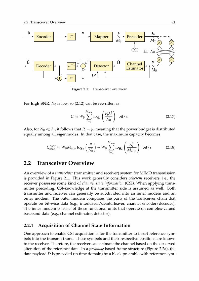
An overview of a transceiver (transmitter and receiver) system for MIMO transmissionis provided in Figure 2.1. This work generally considers coherent receivers, i.e., thereceiver possesses some kind of channel state information (CSI). When applying trans-mitter precoding, CSI-knowledge at the transmitter side is assumed as well. Bothtransmitter and receiver can generally be subdivided into an inner modem and anouter modem. The outer modem comprises the parts of the transceiver chain thatoperate on bit-wise data (e.g., interleaver/deinterleaver, channel encoder/decoder).The inner modem consists of those functional units that operate on complex-valuedbaseband data (e.g., channel estimator, detector).
2.2.1 Acquisition of Channel State Information
One approach to enable CSI acquisition is for the transmitter to insert reference sym-bols into the transmit frame. These symbols and their respective positions are knownto the receiver. Therefore, the receiver can estimate the channel based on the observedalteration of the reference data. In a preamble based frame structure (Figure 2.2a), thedata payload D is preceded (in time domain) by a block preamble with reference sym-

22 Chapter 2. Selected Areas of MIMO Baseband Processing
Time
Freq
uenc
ySpace
P P PP P PP P PP P PP P PP P PP P PP P P
DDDDDDDD
DDDDDDDD
DDDDDDDD
DDDDDDDD
DDDDDDDD
(a) Reference preambleTime
Freq
uenc
y
Space
P
P
P
D
D
D
D
DDDDDDDD
D
D
D
D
DDDDDDDD
D
D
D
D
DDDDDDDD
D
D
D
D
DDDDDDDD
P
P
P
P
P
P
P
P
P
P
P
P
P
(b) Reference pilot symbols
Figure 2.2: Physical layer frame structure with preamble/pilots (P) for channel esti-mation and data payload (D).
bols P. For a complete estimate of the channel, the preamble has to consist of at leastMS OFDM slots. An OFDM slot is also referred to as a preamble slot when locatedwithin the block preamble and as a data slot when located within the payload data.For a preamble based frame structure, the channel estimate is derived once per frame,assuming that the channel state is quasi static during the corresponding time span.This assumption is realistic for slow fading channels that can be expected in indoorscenarios like wireless LAN (see Section 2.1.3). For quickly changing channels (fastfading), the channel estimate has to be updated frequently.3 This requires an evendistribution of pilot symbols in the frame over the spatial, temporal, and frequencydimension [135]. Frame structures with distributed pilot symbols, like in Figure 2.2b,are typically used in cellular standards like LTE [38].
2.2.2 Transmitter
At the transmitter in Figure 2.1, the information bitstream b is encoded and then in-terleaved, resulting in the coded bitstream x. The redundancy added by the encodercan be used at the receiver to correct bit errors. Interleaving provides additional pro-tection against burst errors. This combination of coding and interleaving is referredto as bit-interleaved coded modulation (BICM) [23]. The mapper transforms x into astream of complex-valued transmit symbol vectors s ∈ OMS . The set O comprisesthe alphabet of possible complex-valued constellation symbols. Each constellationsymbol in O has a binary representation (label) of Q bits so that M = |O| = 2Q. Acommon choice for O is a quadrature amplitude modulation with M elements (M-QAM).The precoder generates precoded transmit symbol vectors sa from s by applying a
3 Coherence time according to (2.6) in the 800 MHz band (e.g., LTE [38] in Germany) for a fast movingcar or train at 180 km/h is 937.5 µs in contrast to an OFDM symbol length of 714.3 µs in LTE [38](short CP mode).

2.3. Linear SVD Precoding 23
power allocation scheme followed by a base transformation (see Section 2.3). To thatend, an efficient precoding scheme requires CSI at the transmitter. Next, sa is mod-ulated and transmitted via the antenna interface characterized by channel matrix Haand noise spectral density N0. A common multi-carrier modulation scheme is OFDM(see Section 2.1.2), where the transmit signal is split in the frequency domain into MForthogonal subcarriers. Some of these subcarriers are typically nulled (e.g., in IEEE802.11n [69]) to form a guard band to neighboring channels, so that MF,a ≤ MF ac-tive/used subcarriers remain. Out of these active subcarriers, MF,d ≤ MF,a are usedfor data payload transmission. The remaining MF,p pilot tones can be used for phaseand frequency offset corrections [90]. OFDM is particularly beneficial for frequencyselective fading channels, since a deep fade on one specific subcarrier will only affectthe symbols mapped to that subcarrier. For practical realizations, MF is typically cho-sen as a power of two, so the transformation from frequency domain to time domainat the transmitter can be implemented by an inverse fast Fourier transform (iFFT). Thereverse transformation from time to frequency domain at the receiver can then beimplemented by an FFT.
2.2.3 Receiver
At the receiver, reference symbols within the receive symbol vectors y are used to de-rive an estimate H of the channel matrix H ∈ CMR×MS . In contrast to Ha, H describesthe channel between transmit symbol vector s before precoding, and receive symbolvector y. This estimate is utilized by the MIMO detector to mitigate the impact of thechannel on the transmit vector. A multitude of detection algorithms and implementa-tions have been discussed in the open literature. This work focuses on equalizer-baseddetectors (see Section 2.4.2), due to their relative simplicity and deterministic execu-tion time. The detector delivers a stream LP of a posteriori log-likelihood ratios (LLRs)which are transformed to extrinsic LLRs LE and subsequently deinterleaved and for-warded to the decoder. The decoder then calculates an estimate b of the originallytransmitted information bitstream b, using the previously induced redundancy to cor-rect bit errors. To improve the error correction capabilities of the receiver, a stream LA
of a priori LLRs can be fed back from the decoder to the detector to enable turbo-likeiterations between detector and decoder [58].
2.3 Linear SVD Precoding
The results of the channel capacity analysis in Section 2.1 can be used to design alinear SVD-based precoder in conjunction with a power allocator to narrow the gapbetween achieved data rate and channel capacity. Section 2.3.1 discusses the underly-ing principle and the structure of a linear SVD precoder. Section 2.3.2 illustrates thegains achievable by means of SVD-based precoding for a practical example based onthe IEEE 802.11ac [72] standard.

24 Chapter 2. Selected Areas of MIMO Baseband Processing
2.3.1 Principle
The functionality of a linear precoder can be expressed as
sa = Fs, (2.19)
where F ∈ CMT×MS is the precoding matrix. In case no precoding is applied, Fis an identity matrix, MS = MT, and sa = s. Otherwise, matrix F combines multi-mode beamforming, power allocation, and input shaping [120]. The SVD of precodingmatrix F is given by
F = UFP VHF . (2.20)
The input shaping matrix VF ∈ CMS×MS shapes the covariance of s. In case no covari-ance information is available, the matrix is set to identity. Matrix P ∈ RMT×MS assignsthe power P2
ij to the j-th element of the shaped input vector which is then mappedonto the i-th eigenmode of the channel. The choice of multi-mode beamforming ma-trix UF ∈ CMT×MT depends on the type of CSI that is available at the transmitter.If the instantaneous channel matrix with SVD Ha = UΛVH is known, the optimalchoice is UF = V.
The acquisition of CSI and the resulting latency and inaccuracy are importantfactors for precoder systems. Generally, two different kinds of approaches to channelacquisition can be distinguished [120].
1. Reciprocity: For two communicating nodes A and B, channel matrix Ha,AB forthe transmission from A to B for a specific subcarrier is the transpose of thechannel matrix for the opposite direction of the same subcarrier. Since moderncommunication systems typically operate in duplex mode, it can be assumedthat the precoder at node A can obtain Ha,AB = HT
a,BA based on transmissionsit receives from node B. This method is also referred to as open-loop acquisition,since there is no explicit CSI feedback from B to A. One prerequisite for suchan acquisition scheme is that both transmission directions use the same channel.Strictly speaking, this is neither the case for a frequency-division duplex (FDD) sys-tem nor for a time-division duplex (TDD) system. The two directions of an FDDtransmissions are separated in the frequency domain, so reciprocity only appliesapproximately for narrowband systems where neighboring channels may be as-sumed to be similar. This is not the case for wideband systems, which are ofparticular interest for this work. For a slow fading channel (e.g., wireless LAN)in a TDD system, it is fair to assume, though, that after node A has received atransmission from node B, the channel remains quasi constant for long enoughso node A can use the channel knowledge from the received transmission toprecode the next outgoing transmission. One problem of open-loop feedback isthat reciprocity only applies to the channel itself, but not to the connected userequipment (e.g., radio frequency front end) which also influences the channelmatrix.
2. Feedback: Here, node B estimates Ha,AB and transmits CSI back to A. Therefore,this scheme is also called closed-loop channel acquisition. Since channel reci-

2.3. Linear SVD Precoding 25
6 8 10 12 14 16 18 20 22 24 26 28 30 32 34 36 38 4010−3
10−2
10−1
100
SNR
FER
8x8x8 8x6x8 8x4x8 8x2x8 6x6x6 6x4x6 6x2x6
Figure 2.3: FER for MT=MR = 8 and MT=MR = 6 for variable number of usedeigenmodes. Modulation: 256-QAM. OFDM tones: 64. OFDM datatones: 52. Frame size: 2,304 byte (uncoded). Channel coding: LDPC,codeword length 1944 bit, code rate: 5/6. Channel model: slow fading.
procity is not necessary here, both TDD and FDD schemes are equally suitable.However, the feedback data generates additional data payload, which reducesthroughput. For that reason, extensive research has been conducted as to howthe amount of feedback data can be reduced [83]. Instead of sending the entirechannel matrix, a quantized or compressed version of the CSI is transmitted.A further step is to feedback the actual precoder setup (e.g., precoding matrix)instead of CSI.
2.3.2 Precoding Gains
Figure 2.3 shows the communication performance of MIMO transmission with SVD-based linear precoding as in (2.20) with VF = IMS and MS ×MS identity matrix IMS .Communication performance is shown in terms of frame error rate (FER) as a func-tion of the SNR. Here, as well as for the remainder of this thesis, SNR is given perreceive antenna. Two symmetric antenna setups MT=MR = 8 and MT=MR = 6 arepresented, where the precoder selects the MS strongest eigenmodes. The PHY layerframe structure and the transmission setup are based on the 20 MHz mode of IEEE802.11ac [72] with a block preamble as in Figure 2.2a. The data payload is set to thesize of one MAC service data unit (MSDU) of 2,304 bytes. All use cases use the max-imum code rate of 5/6 and the maximum constellation (256-QAM). Channel codingand decoding are performed by the low-density parity-check (LDPC) algorithm [42, 86]with codewords of length 1944 bit. The channel is simulated as quasi static (slow fad-ing) according to the TGn-C model [36]. The receiver uses an open-loop linear MMSEMIMO detection algorithm (see Section 2.4.2). Two interesting observations are to be

26 Chapter 2. Selected Areas of MIMO Baseband Processing
made based on Figure 2.3. First, it illustrates the gain of eigenmode selection for afixed antenna setup. For the 8× 8 antenna configuration, for example, selecting thesix strongest eigenmodes instead of all eight delivers an SNR gain of approximately12 dB. For the 6× 6 configuration, selecting four out of six eigenmodes even deliversa gain around 15 dB. These gains naturally come at the cost of a reduced data rate.Second, it can be observed that for a fixed data rate, (e.g., MS = 6), there is a spatialdiversity gain [32, 113] of roughly 12 dB when using an 8× 8 antenna setup and se-lecting the six strongest eigenmodes instead of using all eigenmodes of a 6× 6 setup.This gain comes at the expense of a higher computational effort.
2.4 MIMO Detection
A MIMO detector derives an estimate of the originally transmitted coded bit sequencex based on the receive symbol vector y, channel matrix H and further a priori knowl-edge. The detectors presented in this section are aimed at transceiver setups withouttransmitter precoding or without knowledge of the precoding scheme at the receiver.In that case, the receiver is not aware of the transmit antenna setup but only of thenumber of transmit streams MS. Therefore, the detector sees the transmission as
y = Hs + n . (2.21)
A distinguishing property of detectors is the type of information they receive fromand supply to other receiver components.
• Hard-output detectors forward a binary (hard) estimate of the bitstream x to thechannel decoder.
• Soft-output detectors provide additional reliability information in the shape ofLLRs for each bit, where the polarity of the LLR denotes what binary symbolwas supposedly transmitted, while the amplitude indicates the certainty of theestimation.
• Soft-input, soft-output (SISO) detectors deliver LLRs to the decoder and ac-cept additional soft a priori information (e.g., from previous detector-decoderiterations) as input.
It has been shown [63] that soft-output and SISO detectors achieve a significant gain incommunication performance compared to hard-output detectors. For this reason, thiswork focuses on SISO detection schemes. Regarding the type of iterative informationexchange between two transceiver components, two different types of information canbe distinguished.
• Intrinsic information that is passed from functional unit A to unit B, for ex-ample, contains the complete reliability information including information thatwas previously supplied to A by B as a priori information.
2.4. MIMO Detection 27
• Extrinsic information passed from A to B contains only the new informationderived by A and is free of any a priori information previously supplied byB. When using LLRs, intrinsic information can be transformed into extrinsicinformation by subtracting any previously used a priori information from theextrinsic a posteriori information.
For some iterative processes, it is beneficial to exchange only the new, extrinsic infor-mation between different functional units (see Figure 2.1, for example).
Section 2.4.1 describes optimal SISO detection. A drawback of this algorithm isits high computational complexity, which renders it impractical for actual hardwareimplementations. Suboptimal detection, as presented in Section 2.4.2, provides lesscommunication performance but is more suitable for hardware implementations dueto its reduced complexity. Note that for the remainder of this thesis, a bipolar repre-sentation {+1,−1} of coded and uncoded hard information is used for consistencywith the bipolar nature of LLRs.
2.4.1 Optimal Detection
The optimal SISO strategy for coherent MIMO detection minimizes the probability ofmaking a faulty estimate for each bit. It is therefore referred to as maximum a posteriori(MAP) detection. A detailed discussion is available in [63], whereof the followingsection gives a brief summary. The intrinsic a posteriori information for the b-th bitof the i-th stream derived by a MAP SISO detector as in Figure 2.1 is given by
LPi,b = log
(P[xi,b = +1|y, H]
P[xi,b = −1|y, H]
). (2.22)
A priori information about the likelihood of xi,b being either +1 or −1 based on thelast iteration is passed from the decoder back to the detector.
LAi,b = log
(P[xi,b = +1]P[xi,b = −1]
)(2.23)
The extrinsic a posteriori information is given by
LE = LP − LA. (2.24)
This means that LE only contains information that is new to the decoder. This is whyLE is typically forwarded from the detector to the decoder instead of LP. Applyingthe Bayes theorem to (2.22) delivers
LPi,b = log
∑s∈S (+1)
i,b
p(y|s, H)P[s]
− log
∑s∈S (−1)
i,b
p(y|s, H)P[s]
(2.25)

28 Chapter 2. Selected Areas of MIMO Baseband Processing
with
P[s] =∏
i,b:xi,b=+1
exp(
LAi,b
)1 + exp
(LA
i,b
) ∏i,b:xi,b=−1
1
1 + exp(
LAi,b
) , (2.26)
where S (+1)i,b and S (−1)
i,b denote the subsets of transmit symbol vectors whose bit labelfor the i-th transmit stream at the b-th bit position is +1 or −1 respectively. For aMIMO channel with AWGN as in (2.21), the Gaussian approximation delivers
p(y|s, H) ∝ exp(−‖y−Hs‖2
N0
), (2.27)
so (2.25) can be rewritten as
LPi,b = log
∑s∈S (+1)
i,b
exp(−‖y−Hs‖2
N0
)P[s]
− log
∑s∈S (−1)
i,b
exp(−‖y−Hs‖2
N0
)P[s]
. (2.28)
Calculating (2.28) requires iterating over all 2QMS possible symbol vectors. This expo-nential computational complexity renders (2.28) unsuitable for real-time capable hard-ware implementations, particularly when constrained by energy budgets for battery-powered devices.
2.4.2 Suboptimal Detection
The max-log approximation states that the logarithm of a sum of exponential terms canbe approximated by the highest exponent of the summands.
log
(∑i
exp (ai)
)≈ max
i{ai} (2.29)
Since the exponent in (2.28) is a negative fraction, (2.29) states that the minimum of thefraction itself has to be found. Therefore, (2.28) can be approximated as follows [63].
LPi,b ≈ min
s∈S (−1)i,b
{‖y−Hs‖2
N0− log P[s]
}− min
s∈S (+1)i,b
{‖y−Hs‖2
N0− log P[s]
}(2.30)
It has been shown that the approximation in (2.30) has negligible impact on the overallcommunication performance (e.g., FER) [63, 101]. Despite the reduced computationalcomplexity achieved by replacing the sum of exponential terms in (2.28) by a mini-mum distance search, (2.30) still requires a search covering all 2QMS transmit symbol
2.4. MIMO Detection 29
vectors. To be suitable for hardware implementation, further simplifications have tobe made to the algorithm. Sections 2.4.2.1 and 2.4.2.2 present equalizer-based detec-tors that reduce the vectorial search in (2.30) to a scalar search. Despite the reductionin communication performance caused by this simplification, iterative equalizer-baseddetectors can achieve competitive results and have the advantage of deterministic exe-cution time. Sphere detectors on the other hand express the vectorial minimum searchin (2.30) as a tree search problem, where the execution time of the tree search may beindeterministic, depending on the implementation of the search. Even though the fo-cus of this work is on equalizer-based detection, Section 2.4.2.3 gives a brief overviewof sphere detection for comparison.
2.4.2.1 Open-Loop Linear MMSE Detection
Instead of performing a search over the set of transmit symbol vectors in (2.30), alinear detector performs a per-stream search over the scalar constellation symbols [89].To that end, the receive symbol vector is equalized first. Several equalization tech-niques exist (e.g., zero forcing [21]), but this work focuses on minimum mean squareerror (MMSE) based equalization. The idea of linear MMSE MIMO detection was de-veloped in [98] and is depicted in this section. The equalized MMSE symbol vector sis a linear transformation of the receive vector y by an equalizer matrix WH
ol ∈ CMS×MR
that minimizes the expected MMSE among s and transmit symbol vector s.
s = WHoly
WHol = arg min
WHol
E{‖s− s‖2
}(2.31)
From (2.31), it follows for vectors s with uncorrelated entries that
WHol =
(HHH + N0IMS
)−1HH. (2.32)
Based on s, (2.30) is reduced to a scalar search. In the absence of a priori knowledge,
LPi,b ≈ ρi
mins∈O(−1)
b
|si − s|2 − mins∈O(+1)
b
|si − s|2 (2.33)
with post-equalization signal-to-interference-plus-noise ratio (SINR)
ρi =1
N0
[(HHH + N0IMS
)−1]
ii
− 1 (2.34)
and sets O(+1)b and O(−1)
b denoting the subsets of O with a +1 or −1 at position b oftheir respective bit label.

30 Chapter 2. Selected Areas of MIMO Baseband Processing
2.4.2.2 Iterative MMSE-PIC Detection
Open-loop linear detection as presented in Section 2.4.2.1 can be extended to use a pri-ori information to improve communication performance. The MMSE-PIC algorithmis a prominent approach to iterative equalizer-based MMSE detection using parallelinterference cancellation [101, 121]. The concept is briefly illustrated in the following.Based on a priori LLRs, the elements of the most likely transmitted soft symbol vectorz ∈ CMS×1 can be reconstructed as
zi = E {si} =∑a∈O
P [si = a] a, i ∈ {1, . . . , MS}. (2.35)
Based on the observations in [126], (2.35) uses intrinsic a priori information in theshape of posterior LLRs supplied by the channel decoder. A hardware-friendly deriva-tion of z from LA based on small lookup tables (LUTs) for probabilities P [si = a] andfew scalar multiplications and additions is described in [111]. Next, the inter-antennainterference in receive vector y is mitigated using z.
yi = y−∑j 6=i
hjzj, i ∈ {1, . . . , MS} (2.36)
Here, hj denotes the j-th column vector of channel matrix H. The interference mit-igated vectors yi thus are an estimate of what the receive antennas would have re-ceived, if only zi had been transmitted via the i-th transmit stream. Then, MMSEfiltering is applied to each yi by filter vector wH
i ∈ C1×MR according to
si = wHi yi (2.37)
wHi = arg min
wHi
E{|si − si|2
}. (2.38)
From the biased MMSE estimate si, the unbiased estimate follows as
si =wH
i yi
wHi hi
, (2.39)
where wHi is a scaled version of wH
i . It was shown in [101] that all MS filter vectorswH
i can be derived from a single matrix WHit = [w1, ..wMS ]
H given by
WHit =
(HHHΛz + N0IMS
)−1HH. (2.40)
The diagonal matrix Λz ∈ RMS×MS contains the variances of z so that
Λz,ii = Var{zi}. (2.41)

2.4. MIMO Detection 31
As established in [111], these variances can also be calculated based on small LUTs andlow-complexity scalar arithmetic. The extrinsic a posteriori LLRs that are forwardedto the channel decoder can be directly calculated according to
LEi,b ≈ ρi
mins∈O(−1)
b
|si − s|2 − mins∈O(+1)
b
|si − s|2 (2.42)
with post-equalization SINR
ρi =wH
i hi
1−Λz,iiwHi hi
. (2.43)
2.4.2.3 Sphere Detection
The sphere detection algorithm transforms the search over all symbol vectors in (2.28)into a tree search. The mathematical foundation was established by [91] and laterapplied to MIMO detection (e.g., [117]). The following provides a brief synopsis ofthese works. To enable the aforementioned tree search approach, an alternative rep-resentation of the MIMO transmission equation is derived. First, the channel matrixis QR-factorized [45] so that
H = QR , (2.44)QHQ = IMS . (2.45)
Matrix Q ∈ CMR×MS is unitary, and matrix R ∈ CMS×MS is an upper triangular ma-trix with a real-valued diagonal. These properties allow the rewriting of the MIMOtransmission equation in (2.21). Applying a left multiplication by QH results in
y = Rs + n (2.46)
with y = QHy and n = QHn. Since Q is unitary, n has the same statistical propertiesas n and (2.30) can be restated as
LPi,b ≈ min
s∈S (−1)i,b
{‖y− Rs‖2
N0− log P[s]
}− min
s∈S (+1)i,b
{‖y− Rs‖2
N0− log P[s]
}. (2.47)
In the absence of a priori knowledge, the computational essence of (2.47) is to find theminimum Euclidean distance
d(s) = ‖y− Rs‖2 (2.48)
over two distinct subsets of OMS . In contrast to the Euclidean distance in (2.30), d(s)can be calculated recursively due to the triangular structure of R. One recursion cor-responds to selecting one scalar element si from the constellation alphabet O, startingfrom i = MS to 1 so that d(s) = d1.
di = di+1 + |ei|2 (2.49)

32 Chapter 2. Selected Areas of MIMO Baseband Processing
ei = yi −MS∑j=i
Rijsj (2.50)
This recursive calculation scheme allows the representation of the search for the min-imum d(s) as a tree search. The depth of the tree corresponds to the number oftransmit streams, and internal nodes have |O| children.
Since performing an exhaustive search by determining d(s) at all leaf nodes ex-hibits a high computational complexity, reduced complexity tree traversal schemeshave been proposed. The reduced complexity is achieved by pruning, i.e., discardingcertain subtrees of the main tree. Pruning can be performed by constraining di as in(2.49) or by reducing the size of S (+1)
i,b and S (−1)i,b in (2.47), for example. An overview
of tree traversal and pruning methods is provided by [101, 123].
2.4.3 Comparison
This section conducts a comparison of the previously introduced equalizer-basedMMSE and sphere detection4 algorithms. The transceiver setup is chosen according tothe IEEE 802.11n [69] standard using the maximum antenna setup MT=MR = 4 anda 16-QAM constellation. The convolutional channel encoder uses the octal generatorpolynomials g0 = 133o and g1 = 177o at a code rate of 1/2. The corresponding de-coder employs maximum a posteriori decoding according to the BCJR algorithm [85].The channel is simulated as a slow fading channel according to the TGn-C model [36]for a bandwidth of 20 MHz and 64 OFDM tones. One frame consists of four preambleslots and has a data payload of 2,304 uncoded bytes, which corresponds to the size ofone MSDU in the IEEE 802.11 [71] standard.
Figure 2.4 presents FERs for several MIMO detector configurations. For a targetFER of 1 %, a significant advantage of approximately 5.5 dB of the sphere detectorover the equalizer-based MMSE variant in the absence of detector-decoder iterationsis observed. The architectural throughput of current state-of-the-art hardware imple-mentations of 4× 4 MIMO detectors (e.g., [103]) is commonly laid out to support oneor zero iterations for a given communication standard (e.g., IEEE 802.11n [69]). There-fore, it is interesting to see that after the first iteration, the advantage of the spheredetector has already narrowed to around 2.3 dB. In the fourth iteration, it has de-creased further to about 0.7 dB. The aforementioned observations make a strong casefor equalizer-based MIMO detection. It can be argued that the significant reductionin computational complexity, as opposed to sphere detection, is worth the observeddegradation of the FER. The deterministic execution time is another advantage ofequalizer-based detection. Sphere detectors with depth-first tree traversal schemes onthe other hand exhibit an indeterministic execution time [123].
4 The sphere detector considered in this comparison employs no tree pruning, i.e., it performs anexhaustive tree search according to (2.47).

2.4. MIMO Detection 33
10 12 14 16 18 20 22 2410−3
10−2
10−1
100
SNR
FER
MMSE it-0 MMSE it-1 MMSE it-2 MMSE it-4Sphere it-0 Sphere it-1 Sphere it-2 Sphere it-4
Figure 2.4: Comparison of MIMO detection algorithms. FER for MT=MS=MR = 4.Modulation: 16-QAM. OFDM tones: 64. OFDM data tones: 52. Framesize: 2,304 byte (uncoded). Channel coding: convolutional (g0 = 133o,g1 = 177o), code rate: 1/2. Channel decoding: BCJR. Channel model:slow fading.

34 Chapter 2. Selected Areas of MIMO Baseband Processing

Chapter 3
Multi-Platform, Multi-StandardSimulation Testbed
The research activities conducted within this work involve embedded software devel-opment for third party platforms, ASIP design (including the respective firmware),as well as custom ASIC design. While the nature of all of these implementations isfundamentally different, they are all intended for the application domain of MIMObaseband processing. Therefore, consistency and comparability demand the use of acommon testbed for verification and exploration of the aforementioned target archi-tectures. In this context, verification means to assess whether a specific componentdelivers the expected theoretical communication performance. Exploration coversdetermining which numerical parameters are needed to deliver the aforementionedperformance, for example. Section 3.1 elaborates on different metrics for communica-tion performance and presents the metric of choice that is used for the remainder ofthis thesis. Section 3.2 describes the flow according to which the functionality of hard-ware and software developed within this work is verified and the impact of variousnumerical parameters can be explored. Section 3.3 then presents the actual testbedthat implements this flow. Finally, Section 3.4 introduces an extension to the testbedthat allows to insert actual hardware (e.g., evaluation boards) into the verificationflow.
3.1 Evaluation of Communication Performance
With respect to communication performance, there are several potential performancemetrics, each of them with their respective advantages and disadvantages. The fol-lowing gives a brief overview.
• The uncoded bit error rate (BER) indicates the fraction of faulty bits in the post-detection LLR stream LP compared to the coded information x (see Figure 2.1).Since the hardware and software implementations investigated in this work alloperate on coded data, the BER of the code bits (i.e., hard decision on the LLRstream before decoding) seems to be a possible performance indicator at firstglance. However, this error rate does not allow a reliable prediction of the BERafter decoding of the channel code and, thus, of the communication performanceexperienced at the higher layers of the communication system. In particular, thecomparison of post-detection LLRs with a bipolar input sequence neglects thequality of the soft-information, which has significant impact on the efficiency ofchannel coding [63].
35

36 Chapter 3. Multi-Platform, Multi-Standard Simulation Testbed
• Mutual information or transinformation is a information-theoretical perfor-mance indicator that measures how much common information is containedin two random variables (e.g., LP and x) [92]. Therefore, mutual informationconsiders the actual quality of the soft-information within LP. For this reason,it is a more complete performance indicator for post-detection LLRs than theuncoded BER. However, for practical implementations with imperfect channelencoders and decoders, it cannot be guaranteed that the complete mutual infor-mation is actually extracted by the employed coding scheme. Therefore, mutualinformation is merely an upper bound for the communication performance thatcan potentially be experienced by higher layers.
• The coded bit error rate is the fraction of faulty bits when comparing the origi-nal information b with the reconstructed post-decoding information b. Accord-ingly, the performance of channel coding is implicitly contained in the perfor-mance metric, which renders it more relevant for the evaluation of a practicalcommunication system. On the other hand, the coded BER is less general thanmutual information, since it is specific for the selected channel coding scheme.In the context of common communication standards like IEEE 802.11, one alsohas to consider that at the receiver, data is accepted as correct or consideredlost in transmission in certain granularities called frames or protocol data units(PDUs) [90]. The coded BER alone, however, gives no indication with respect tothe distribution of bit errors (e.g., whether errors occurred clustered in one PDUor spread across multiple PDUs).
• The frame error rate (FER) denotes the fraction of compromised frames/PDUswithout concern for any internal error distribution. It is well suited as a metricto describe the communication performance supplied to the upper layers of acommunication system. A potential problem lies in the aspect of comparabil-ity. It is intuitively sound that the error probability of a frame rises along withits size. Therefore, FERs from the literature can only be compared if they usethe same frame size. However, there is more than one rational regarding thedefinition of frame size, particularly for comparison among different use cases(e.g., different code rates, number of antennas, etc.). Depending on the angle ofinvestigation, frame size may be interpreted as time domain duration, numberof transmit symbols, transmit vectors, coded bits, or information bits.
Even though the testbed presented in this chapter can generate all of the afore-mentioned metrics, the communication performance figures shown in this work areFERs or FER-based. This choice was made because the focus of this work is on thepractical implementation of physical (PHY) layer hardware and software for commu-nication scenarios based on actual communication standards. As the layers abovePHY according to the ISO OSI reference model [132] accept or reject received datain the granularity of frames regardless of the error distribution in the frame, FERis the most suitable unit to express the communication performance delivered to theupper layers of the respective communication standard. As mentioned above, a mean-

3.2. Exploration and Verification Flow 37
ingful comparison of FERs requires a fixed definition of the frame size. Since IEEE802.11 [71] is an important use case for the implementations presented in this work,the frame size definition is based on that standard. IEEE 802.11 [71] operates onthe PHY layer and the medium access control (MAC) layer [90]. The payload data ex-changed among the MAC layer and the next higher protocol layer is bundled intoMAC service data units (MSDUs). Within the MAC layer, an MSDU is extended byfurther meta data (e.g., address field) to form a MAC protocol data unit (MPDU). Themaximum MSDU size defined by IEEE 802.11 [71] is 2,304 bytes. As the focus of thiswork is on the PHY layer, the testbed presented in this chapter does not include anyrouting or multi-user aspects. This means that there is no MPDU meta data, and thedata passed between the MAC and PHY layer corresponds to the size of one MSDU.For maximum throughput, it is assumed that MSDUs are always filled to up to theirmaximum size. Therefore, the coded data payload of a PHY layer service data unit(PSDU) always contains 2,304 bytes of uncoded information, regardless of the actualcode rate. Adding further meta data (e.g., preamble sequence for channel estimation)forms the complete PHY protocol data unit (PPDU) which is also referred to as a PHYlayer frame. Thus, unless specified otherwise, the size of a PHY layer frame is definedby a fixed number of 18,432 information bits for the remainder of this work. Theactual time domain duration depends on further PHY layer parameters (e.g., symbolconstellation, number of used eigenmodes, code rate, etc.).
3.2 Exploration and Verification Flow
The flow for hardware/software exploration and verification is outlined schematicallyin Figure 3.1. The starting point for any implementation is a functional algorithm evalu-ation, where the communication performance of a specific algorithm is evaluated. Forthat purpose, the algorithm is implemented in a high-level programming language(here C++) and integrated into a transceiver testbed including a wireless channel sim-ulator. For ease of programming, the development environment already contains avector arithmetic support library [47]. All arithmetic operations are performed us-ing the double-precision floating-point number format to eliminate the impact ofnumerical aspects onto communication performance. Once the algorithm has beenfunctionally verified, numerical algorithm exploration determines a first estimate of thenumerical parameters (e.g., wordwidth) that are required to achieve the previouslyestablished communication performance. To that end, the transceiver testbed offersemulation libraries for custom fixed-point and floating-point number formats. Sinceat this point, the data flow in the simulator does not match the data flow in the finalhardware implementation, yet, the results obtained at this state might still be sub-ject to change. During numerical hardware/software exploration, on the other hand, thetestbed uses a bit-accurate model of the target hardware provided by a host supportlibrary (HSL). For ASIC design, the hardware model consists of a piece of a softwarethat uses the custom number format libraries and follows the data flow of the ASICto implement the desired functionality. For the design of programmable architectures

38 Chapter 3. Multi-Platform, Multi-Standard Simulation Testbed
Functional Algorithm Evaluation(full precision floating-point)
Numerical Algorithm Exploration(custom number format)
Numerical HW/SW Exploration(bit-accurate)
ADL/SW SW
Layout
CrossCompiler
RTLGeneration
DemoBoard
TestbedTransceiver
ModelReference
HWSynthesis
RTL
Stim.HSLH
DL
Sim
ulat
or
Figure 3.1: Exploration and verification flow.
and their corresponding software, a two-step approach is used. First, a bit-accuratefunction for each instruction in the envisioned instruction set is implemented in ahigh-level programming language. These mimic functions are designed to resemblethe assembly language of the target architecture as much as possible. Then, the targetapplication is build as a composition of mimic functions. This flow has two mainbenefits: First, there will already be an initial version of the assembly software thatcan serve as a starting point for the actual implementation. Second, the one-on-onerelationship among mimic instructions and assembly instructions allows for an in-depth, instruction-level verification of the processor model against the testbed imple-mentation. In this work, programmable architectures are described by an architecturedescription language (ADL)1. The ADL model and the HSL model both generate XMLdumps that contain relevant data for each instruction executed (e.g., instruction name,operands, result). Therefore, bugs or mismatches can be detected easily and early inthe hardware design process. Integrating HSLs into the transceiver testbed also en-ables the simulation of software written for third-party platforms, since DSP vendors(e.g., TI) often provide HSL source code or binaries. Based on these bit-accurateprocessor models, extensive simulations are conducted to assure that the implemen-tation on the target hardware delivers the expected communication performance. Forsoftware development for third-party platforms, the exploration and verification flowstops at this point. For ASIC design, the verification and exploration flow continues tolower hardware abstraction levels from register-transfer level (RTL) via gate level down
1 Specifically the Language for Instruction Set Architectures - LISA [134] by Synopsys®.

3.2. Exploration and Verification Flow 39
to layout level. For programmable architectures, there is an additional level basedon ADL. On all abstraction levels, the hardware is verified against the same hardware(HW) reference model. This model uses the same HSL as the transceiver testbed tocreate an input-output equivalent golden reference.
The separation of the transceiver testbed from the HW reference model is a con-scious choice to facilitate fast and efficient exploration and verification. Instead ofcoupling the transceiver testbed with the HDL simulator to verify the communicationperformance of the hardware implementation, the workflow used in this work veri-fies the match of the HSL-based HW reference model and the HDL model (on RTL,gate and layout level) first. Once the matching of the HW reference model and theHDL model is guaranteed, numerical exploration can be conducted independentlyusing the transceiver testbed and the HSL of the current module under test (MUT). Thisanalysis can be performed in a highly parallel manner (e.g., using a compute-cluster).Due to the wide design space, particularly for the napSVD ASIC (see Chapter 6), thisproperty is an absolute necessity. The matching of the HW reference model and theHDL model is verified by means of input-output tests. The stimuli are read by theHW reference model that is aware of the timing behavior of the MUT on a cycle accu-rate level and therefore can read out and verify the results of the MUT at the correcttime. The HDL simulator itself is described on RTL and contains a wrapper for theMUT. The interface of the MUT wrapper is generic regardless of the current abstrac-tion level (RTL, gate level, layout). Accordingly, the same HDL simulator can be usedto verify the MUT on all abstraction levels. Also, since the transceiver testbed and theHW reference model are decoupled, the stimuli to the HDL simulator can but do nothave to come from the transceiver testbed.
Despite the merits of the above described separation of the transceiver testbedand the HW reference model, singular occasions may occur where a tighter couplingis desirable. One example is the use of demonstration boards as a proof-of-concept.In the scope of this work, a TI SDR platform was coupled with the transceiver testbedto showcase the SDR application described in Chapter 4, and to demonstrate its func-tionality on the actual target hardware. Naturally, it is possible to generate a set ofstimuli from the transceiver testbed and use them as input to the application run-ning on the demonstration board. A disadvantage of this setup is the high amount ofstimuli that have to be generated to verify a huge set of relevant use cases (e.g., dif-ferent communication standards, SNRs, constellations, antenna setups). For a morestreamlined verification flow, the transceiver testbed also supports a direct inclusionof demonstrator hardware into the simulated transceiver structure itself. Due to themodular structure of the simulator (see Section 3.3), each block of the transceiver class(e.g., receiver modem or arbitrary subsections thereof) can be overloaded, as long asthe interface to the rest of the transceiver remains the same. Therefore, it is possible tooverload a transceiver block so that it sends data to an external demonstration hard-ware for processing, receives back the results and feeds them back into the remainingprocessing flow. Communication among the transceiver testbed application and thedemonstration board to send and receive stimuli and results can be established byEthernet, for example.

40 Chapter 3. Multi-Platform, Multi-Standard Simulation Testbed
3.3 Modular Testbed
Within the scope of this work and during related research and project activities, amultitude of different communication systems have been evaluated in the context ofdifferent communication standards and use cases. For the sake of a streamlined ver-ification process with comparable, reproducible results, all theses systems have beenevaluated using the testbed described in this chapter. The foundation of this testbedis formed by a floating-point reference communication simulator, programmed inC++. The core algorithmic components are provided by the UPEG2, a versatile C++library of communication algorithms. The functionality provided by the UPEG li-brary is used to generate a modular testbed to mimic the communication chain asdepicted in Figure 2.1, including a model of the wireless channel. Within the mod-ular testbed, each transceiver system is represented by its own C++ class, and thefunctional subblocks are implemented by corresponding C++ methods. This divisionis of hierarchical nature progressing from coarse-grained to fine-grained fractions ofthe transceiver. On the highest level, the system is divided into transmitter, channeland receiver, where the latter is then further subdivided into an inner modem, oper-ating on complex-valued baseband data, and an outer modem, working on a bitwisedata representation. The inner modem, in turn, consists of components like detector,channel estimator, etc., which can be represented based on UPEG functionality. Com-bined, this setup provides the functionality of an entire reference transceiver systemencapsulated into a single C++ simulation class.
Each simulation class that evaluates the performance of a specific hardware com-ponent inherits (in terms of object-oriented programming) from the aforementionedreference simulation class and overloads only the method representing the hardwarecomponent under investigation. This approach guarantees that the hardware emu-lator is embedded into a complete and functional testing environment and that allderived performance data is comparable to data obtained from the reference imple-mentation. The relevant methods are typically overloaded using the functionality ofthe HSL (see Section 3.2) of the target hardware to provide a bit-accurate represen-tation of the corresponding hardware component. This way, the hardware compo-nent can be tested in an otherwise ideal environment. The concept is illustrated inFigure 3.2, where a class for the evaluation of a detector design is inherited fromthe floating-point reference simulation class and the detector method is overloaded.This type of setup is used to analyze the communication performance of the napCorearchitecture (see Chapter 5), for example.
3.4 Integration of Demonstrator Platforms
In the flow described so far, evaluation and verification of communication softwarefor third-party platforms is conducted by overloading certain methods of the refer-
2 Despite there being no publication to cite on the UPEG library itself, the author would like to thankformer colleague Martin Senst for providing this valuable evaluation and verification tool.

3.4. Integration of Demonstrator Platforms 41
Inner ModemTX Modem
Interleaver
Ch. Encoder
Precoder
Modulator
Outer Modem
Channel
RX ModemInner ModemCh. Estimator
Detector
Deinterleaver
Ch. Decoder
Outer Modem
Floating-Point Reference Simulation Class
Inner ModemTX Modem
Interleaver
Ch. Encoder
Precoder
Modulator
Outer Modem
Channel
RX ModemInner ModemCh. Estimator
Detector
Deinterleaver
Ch. Decoder
Outer Modem
Detector Simulation Class
Figure 3.2: Modular transceiver testbed design. Exemplary detector simulation classinherits all methods from reference simulation class (gray) and overloadsdetector method (green).
ence simulation class with a bit-accurate model of the target hardware. It is, however,not necessary that the actual computational task is performed by the simulator. TheC64x+ DSP [106] by TI is one of two major target platforms for the software case stud-ies in Chapter 4. It is used in many TI platforms, like the TMS320C6474 [108] whichincorporates three C64x+ cores as well as communication specific hardware accelera-tors for certain tasks that would be too costly (e.g., in terms of execution time) whenexecuted in software. In case of the TMS320C6474 [108], the VCP2 and TCP2 copro-cessors are included for Viterbi and Turbo channel decoding. The TMS320C6474 [108]is also commercially available embedded into the TMDSEVM6474L evaluation plat-form [35], including further peripherals (e.g., Ethernet adapter). Moreover, TI suppliesthe network developer’s kit (NDK) [109], a software collection to support TCP/IP com-munication, build on top of TI’s real-time operating system SYS/BIOS [110]. Usingthe above mentioned software tools, the TMDSEVM6474L [35] is connected to a hostmachine running the transceiver testbed described in Section 3.2 and 3.3. The TCP/IPsoftware stack on the TMDSEVM6474L [35] receives data from the simulation testbedand hands it to the receiver modem software described in Chapter 4. Afterwards,the processed data is passed back to the simulation testbed via TCP/IP. The testbedon the host side inherits a simulation class where the entire receiver modem is over-loaded with a communication routine that sends complex-valued receiver basebanddata to the demonstration board and receives back the uncoded information streamwhich is then used to generate error statistics. Such a demonstration setup is valu-able to verify that the developed software behaves as expected on the target system.Furthermore, while there are bit-accurate HSLs for the C64x+ instruction set, there

42 Chapter 3. Multi-Platform, Multi-Standard Simulation Testbed
Figure 3.3: Standalone demonstration setup with TMDSEVM6474L [35] evaluationplatform and host computer.
are no bit-accurate simulators for the VCP2 and TCP2 coprocessors. For that reason,it is important to verify that the communication software interfaces correctly withthe channel decoders and the desired communication performance is achieved on thetarget hardware.
For demonstration purposes, it is sometimes necessary to showcase the functional-ity of SDR software on a demonstration platform like the TMDSEVM6474L [35] with-out including the transceiver testbed. This has proven particularly beneficial whenworking with third parties who might want to apply their own stimuli sets to thedemonstration platform. For that reason, a second standalone approach for commu-nication performance evaluation on the demonstration platform was designed. Forstandalone simulation, a stimuli storage format based on the Extensible Markup Lan-guage (XML) [15] for receiver verification was defined. The format contains a numberof use case specific parameters (e.g., frame structure, preamble type, number of an-tennas, etc.) along with the complex-valued receiver baseband data. To enable theevaluation of error statistics, the originally transmitted information bits are includedas well. Just as for the evaluation using the transceiver testbed, the board is connectedto a host computer via Ethernet. Also, the software on the demonstration board re-mains the same. Instead of using the transceiver testbed to communicate with thedemonstration board, a demonstration client on the host computer parses the XMLfile and provides the demonstration board with the same TCP/IP communicationinterface as the transceiver testbed. The parsed payload is transmitted to the demon-stration board and the results are compared with the message decoded by the boardto generate error statistics. The transceiver testbed developed within this work alsocontains an XML composer to generate stimuli for standalone simulation. Figure 3.3shows the aforementioned standalone setup with the TMDSEVM6474L evaluationplatform [35] connected to a laptop.
Chapter 4
The Nucleus Methodology:Application Analysis and Synthesis
In the last two decades, wireless communications has become a wide domain withmany different communication standards and application scenarios. The variety ofwireless communication standards like IEEE 802.11a/b/g/n/ac [69,71,72], GSM [39],UMTS [40] and LTE [38] has motivated the use of programmable SDR platforms forPHY layer processing. Instead of integrating an ASIC for each communication stan-dard, SDR implements the different standards in software, supplemented by config-urable hardware accelerators for tasks that are unsuitable for a pure software solution.Ideally, the result of such an approach is that support for an additional communica-tion standard can be realized solely by a software update.
To facilitate the rapid development of new communication software, previousworks (e.g., [96]) have envisioned the Nucleus methodology which this chapter isbased upon. As briefly introduced in Chapter 1, the core idea of the Nucleus method-ology is to analyze the functional blocks of a set of communication standards withrespect to their algorithmic realizations and identify the recurring computational ker-nels that generate the major computational load. The purely algorithmic represen-tation of such a kernel is referred to as a Nucleus. Ideally, this analysis delivers amanageable set of Nuclei, so the entire application can be described as a compositionof Nuclei embedded into a surrounding control flow. For every target platform, eachNucleus has at least one corresponding Flavor, a highly optimized, platform-specificimplementation. The set of all Flavors developed for a specific platform constitutesthe Flavor library. Concentrating the development and optimization effort on thispotentially small library guarantees the overall efficiency of the developed software.Also, this approach separates the computational load from the surrounding controlflow. This is beneficial because the control flow can commonly be represented byplatform-independent constructs of a programming language (e.g., branches, loops,function calls). The Flavors, on the other hand, are highly platform-specific, but theirinterface (e.g., function headers) can be kept generic. Therefore, the control flow canbe implemented by platform-independent frame code that calls the respective Flavorsfor the target platform.
Depending on the target platform, Flavors may have different shapes. For maxi-mum flexibility and rapid development, it is desirable that as many of them as possi-ble can be implemented in software. However, the high data rates and strict latencyconstraints of modern communication standards might impose the use of specializedhardware accelerators for certain Flavors. In the context of digital signal process-ing for wireless communications, channel decoding is a typical example of such a
43

44 Chapter 4. The Nucleus Methodology: Application Analysis and Synthesis
case. The irregular permutation patterns and specialized operations as well as itsindependence of further use case parameters like antenna setup or constellation al-phabet make it a suitable candidate for a tailored hardware accelerator. In line withthis reasoning, common SDR platforms like the TI TMS320C6474 [108] or the InfineonX-Gold SDR2x [95] contain accelerators for Viterbi and Turbo channel decoding. Moreadvanced platforms like the TI TMS320TCI6618 [82] contain further accelerators forbit-interleaving or FFT, for example.
There are two particular cases where the Nucleus methodology shows its strengthto enable fast and efficient development of communication applications. The first caseoccurs when implementing new communication standards. A cellular standard likeLTE [38] and a local-coverage standard like IEEE 802.11 [71] wireless LAN have differ-ent requirements for mobility and therefore different PHY layer frame structures andchannel estimation schemes. Still, a considerable part of baseband processing (e.g.,MIMO detection) is similar. Therefore, the implementation of a new standard can belargely based on Flavors already developed for other communication standards. Thesecond case is the migration of a set of communication standards from one platformto another. Migrating the Flavor library to the new target platform is inevitable, butit will be demonstrated in this chapter that the Flavor library typically is sufficientlysmall, so the migration effort is manageable. As mentioned before, the frame coderepresenting the control flow of each communication standard can be migrated with-out any adaptation. Overall, this minimizes the migration effort, even if the respectivetarget platforms are fundamentally different.
Previous work [96] suggests an iterative, two-phase optimization process for themapping of a communication application to a heterogeneous target platform. Thefirst step consists of a mapping of Nuclei to Flavors, which means deciding how a cer-tain part of the application is executed on the target platform. This is important, sincethere might be more than one Flavor that matches a Nucleus (e.g., execution on a DSPor a hardware accelerator). The second step is the temporal and spatial mapping.Here, a decision is made regarding on which processing element (PE) and at what timethe selected Flavor is executed. This process is repeated in an iterative fashion until allconstraints are met and the objective function of the optimization process has reacheda (local/global) extremum. Typical constraints for communication applications arethe throughput and latency requirements of the respective communication standards.Exemplary objective functions could be power/energy consumption or resource uti-lization. Despite the interesting challenges of application mapping, the focus of thischapter is on multi-standard support and application porting, which mainly involvesNuclei identification, Flavor library development and the writing of frame code. Au-tomatic tools for application mapping to heterogeneous multiprocessor system on chip(MPSoC) platforms are provided by the MAPS tool suite [25], for example.
Section 4.1 presents the analysis of the PHY layer of two wireless communica-tion applications according to the Nucleus methodology. One of these applicationsis based on IEEE 802.11n [69] wireless LAN and the other is derived from the cel-lular LTE [38] standard. For both cases, the receiver application is analyzed andthe corresponding Nuclei are identified. Section 4.2 introduces two SDR processor

4.1. Nucleus Analysis: Baseband Receiver for Wireless Communications 45
cores that are investigated as targets for the previously analyzed communicationstandards. The first is the STxP70 processor by ST Microelectronics, used in MP-SoCs like the P2012/STHorm platform [10]. The second processor core is the TITMS320C64x+ [106] (or short C64x+) very long instruction word (VLIW) DSP as usedby the previously introduced TMS320C6474 platform [108]. Section 4.3 explores thealgorithmic design space spanned by potential implementations of the previously an-alyzed application. Section 4.4 choses a suitable candidate from that design space andpresents the implementation of the aforementioned baseband receiver on both targetprocessors. Section 4.5 discusses the findings of this chapter.
4.1 Nucleus Analysis: Baseband Receiver for WirelessCommunications
This section presents a case study showcasing the Nucleus methodology. Two PHYlayer communication schemes are analyzed in this context. The first one is a wirelessLAN variant based on IEEE 802.11n [69]. The second scheme is designed for cellularcommunication and is based on LTE [38]. Neither of these communication schemesmatch the respective standard exactly. The main differences lie in the transmit andreceive outer modem. Since this work focuses on inner modem components, theremaining parts of baseband processing have been simplified and unified. None of theinvestigated communication schemes contain a scrambler. Instead, the outer modemscontain a single encoder-interleaver or deinterleaver-decoder pair, regardless of thecurrent use case. IEEE 802.11n [69], in contrast, defines a two-encoder setup whenoperating in high throughput mode.
The resulting transceiver setup is depicted in Figure 4.1 which is a more specificversion of the general setup shown in Figure 2.1, excluding precoding (i.e., MT = MS).IEEE 802.11n [69] and LTE [38] both employ OFDM modulation and demodulation incombination with a CP for protection against inter-symbol interference. OFDM sys-tems typically reserve certain subcarriers for specific purposes. Some subcarriers atthe borders of the channel band are zeroed to reduce interference with transmissionson adjacent frequencies. Others are used for synchronization purposes. The subcarriermapper at the transmitter side adds these dedicated subcarriers to the data payloadand they are removed again by the subcarrier demapper at the receiver side. From thePHY layer baseband perspective, the main difference between wireless LAN and cel-lular communication is channel estimation. For the purpose of pilot aided channelestimation, the transmitter injects pilot symbols into the payload, which are used atthe receiver to estimate the channel. The distribution of pilot symbols in the PHY layerframe with respect to time, frequency and space is defined according to the mobilityrequirements of the respective standard (see Section 2.2.1). These requirements arefundamentally different when comparing wireless LANs, designed for low speeds orstatic terminals, and cellular networks, hardened for use in high speed trains, for ex-ample. Accordingly, channel estimation for these two standards is also fundamentallydifferent, as will be discussed in Section 4.1.2.
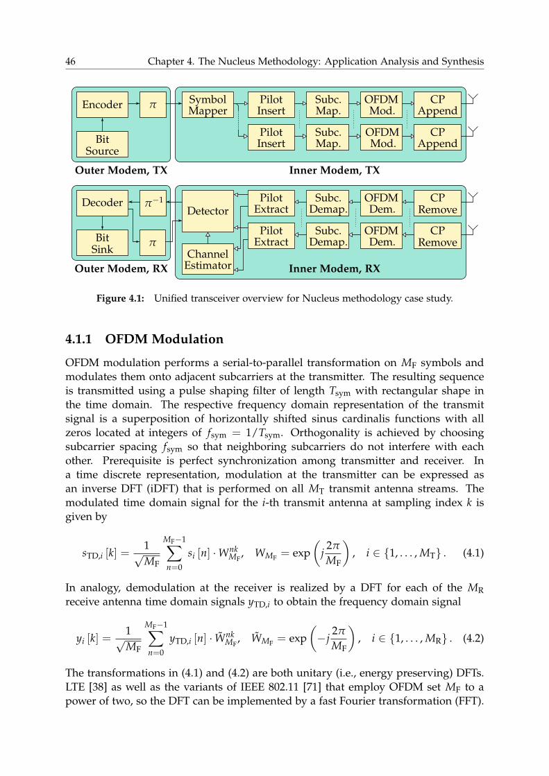
46 Chapter 4. The Nucleus Methodology: Application Analysis and Synthesis
Encoder
Decoder
π
π−1
SourceBit
Outer Modem, TX
MapperSymbol
InsertPilot
Map.Subc.
Map.Subc.
AppendCP
AppendCP
Inner Modem, TX
RemoveCP
RemoveCP
Demap.Subc.
Demap.Subc.
InsertPilot
ExtractPilot
ExtractPilot
Detector
SinkBit
EstimatorChannel
Outer Modem, RX Inner Modem, RX
Mod.OFDM
Mod.OFDM
Dem.OFDM
Dem.OFDM
π
Figure 4.1: Unified transceiver overview for Nucleus methodology case study.
4.1.1 OFDM Modulation
OFDM modulation performs a serial-to-parallel transformation on MF symbols andmodulates them onto adjacent subcarriers at the transmitter. The resulting sequenceis transmitted using a pulse shaping filter of length Tsym with rectangular shape inthe time domain. The respective frequency domain representation of the transmitsignal is a superposition of horizontally shifted sinus cardinalis functions with allzeros located at integers of fsym = 1/Tsym. Orthogonality is achieved by choosingsubcarrier spacing fsym so that neighboring subcarriers do not interfere with eachother. Prerequisite is perfect synchronization among transmitter and receiver. Ina time discrete representation, modulation at the transmitter can be expressed asan inverse DFT (iDFT) that is performed on all MT transmit antenna streams. Themodulated time domain signal for the i-th transmit antenna at sampling index k isgiven by
sTD,i [k] =1√MF
MF−1∑n=0
si [n] ·WnkMF
, WMF = exp(
j2π
MF
), i ∈ {1, . . . , MT} . (4.1)
In analogy, demodulation at the receiver is realized by a DFT for each of the MRreceive antenna time domain signals yTD,i to obtain the frequency domain signal
yi [k] =1√MF
MF−1∑n=0
yTD,i [n] · WnkMF
, WMF = exp(−j
2π
MF
), i ∈ {1, . . . , MR} . (4.2)
The transformations in (4.1) and (4.2) are both unitary (i.e., energy preserving) DFTs.LTE [38] as well as the variants of IEEE 802.11 [71] that employ OFDM set MF to apower of two, so the DFT can be implemented by a fast Fourier transformation (FFT).

4.1. Nucleus Analysis: Baseband Receiver for Wireless Communications 47
Nucleus Parameters Value Equation
FFT num. of symbols MF (4.2)iFFT num. of symbols MF (4.1)
Table 4.1: Nuclei identification for OFDM modulation and demodulation.
FFT and iFFT are reformulations of DFT and iDFT that recursively subdivide the sumsin (4.2) and (4.1). The number of newly created subsums per division is referred toas the radix R of the transformation, and the process of subdividing all sums denotesan FFT/iFFT stage The division is continued until only sums with R inputs remain.Therefore, a Radix-R FFT of length M contains logR(M) stages. While the traces ofthe algorithm date back to Carl Friedrich Gauss in 1805 [60], the first variant targetingdigital signal processing was published in 1965 [29]. The complexity of the algorithmin [29] is O(M log M) as opposed to O(M2) in (4.2) and (4.1). The first division of asignal x of length M for a Radix-2 DFT according to [29] is given by
X [k] = DFTM (x [k]) =M/2−1∑
n=0
x[2n] · W2nkM +
M/2−1∑n=0
x[2n + 1] · W(2n+1)kM
=M/2−1∑
n=0
x[2n] · W2nkM + Wk
M
M/2−1∑n=0
x[2n + 1] · W2nkM
= DFTM/2 (x[2k]) + WkM ·DFTM/2 (x[2k + 1]) , (4.3)
where DFTM denotes a DFT with an input size of M complex-valued scalars. Thisprocess can be repeated until only DFTs of size two and multiplications with twiddlefactors (i.e., powers of WM) remain. The Nuclei involved in OFDM modulation arelisted in Table 4.1.
4.1.2 Channel Estimation
An IEEE 802.11n [69] PHY layer frame stores its pilot symbols in a block preamble thatspans all transmit streams and subcarriers and is located at the temporal beginningof the frame. The frame size is chosen sufficiently small, so it can be assumed thatthe channel estimation based on the up-front preamble is valid for the duration ofthe entire frame. In order to derive an estimate H of the channel matrix H for oneparticular subcarrier, a pilot matrix AP ∈ CMS×MA with MA ≥ MS is transmitted.The column vectors of AP denote temporally distributed transmit vectors filled withpilot symbols. In the following, it is assumed that the minimum sufficient number oftransmit pilot vectors is used (i.e., MA = MS). The receive pilot matrix YP ∈ CMR×MS
contains the corresponding temporally distributed receive vectors so that
YP = HAP + N. (4.4)

48 Chapter 4. The Nucleus Methodology: Application Analysis and Synthesis
Matrix N ∈ CMR×MS denotes the respective composition of AWGN vectors.
4.1.2.1 Frequency Domain Estimation
The most straight forward approach to channel estimation is to derive a frequencydomain (FD) estimate H of H for each subcarrier separately. For a frequency domain,least squares (FDLS) estimation, the noise term in (4.4) is discarded. If the rows of APare linearly independent, (APAH
P ) has full rank and the estimate
H = YPAHP
(APAH
P
)−1(4.5)
is derived based on the right-hand pseudo-inverse of AP. In case AP is also chosen tobe (scaled) unitary so that APAH
P = aIMS , a ∈ R, (4.5) can be simplified further [52].
H =YP
aAH
P (4.6)
4.1.2.2 Time Domain Estimation
Since the sampled channel impulse response of length L is typically shorter than theOFDM symbol length, matrices H are correlated in the frequency domain. This factcan be exploited by means of a time domain (TD) channel estimation. TD channelestimation starts up from the results delivered by FD estimation for each relevantsubcarrier. This means the FD estimate of the paths from each transmit antenna toeach receive antenna is derived first, according to (4.6). TD channel estimation isthen performed for all single input, single output channels formed by the set of allpossible transmit-receive antenna pairs. The following gives a brief overview of singleinput, single output TD channel estimation. For more details, the interested reader isreferred to [57], for example.
Let B ∈ CMF×MF be a diagonal matrix containing the pilot symbols of a singletransmit antenna for each of the MF subcarriers. Vector h ∈ CMF×1 denotes the FDchannel impulse response from the same antenna to a specific receive antenna. Thereceived FD signal is given by
yP = Bh + n, (4.7)
where n ∈ CMF×1 is the per-subcarrier noise vector. Now let g ∈ CL×1 be the sin-gle input, single output TD channel impulse response with a maximum length of Lsamples and FL ∈ CMF×L a DFT matrix to transform vector g to FD. With these newvariables, (4.7) can be rewritten as
yP = BFLg + n. (4.8)
Based on (4.8), the least squares estimate g of the TD channel impulse response isderived by discarding the noise vector and applying the left-side pseudo inverse ofBFL.
g =((BFL)
H BFL
)−1(BFL)
H yP (4.9)

4.1. Nucleus Analysis: Baseband Receiver for Wireless Communications 49
Using TD signal g, the FD signal h is derived by applying DFT matrix FMF .
h = FMF
((BFL)
H BFL
)−1(BFL)
H yP (4.10)
The entire matrix preceding vector yP in (4.10) depends only on the preamble and theOFDM setup. Therefore, it can be computed offline. Moreover, the expression canbe simplified if BHB = bIMF with b ∈ R. This condition is fulfilled, if all constella-tion symbols have the same amplitude, which is a reasonable assumption, since pilotsymbols are typically chosen from a binary phase shift keying (BPSK) constellation [71].
h = FMF
(FH
L FL
)−1FH
LBH
byP (4.11)
Since FL is unitary and the last two factors in (4.11) correspond to the FD estimatehFD (see (4.6)), one can also write
h = FMFFHL hFD. (4.12)
This particular simplification only applies when estimating the FD coefficients of allMF subcarriers, which is referred to as complete training in [57]. The computation of(4.12) can now be efficiently implemented by transforming frequency domain estimatehFD from FD to TD, discarding all except for the first L samples and transforming theresult back to FD. This process is intuitively sound, since L is the assumed TD channelimpulse length. Therefore, all TD samples after the L-th position can be safely zeroed.
4.1.2.3 Interpolation
For PHY layer frame structures with distributed pilot symbols (e.g., LTE [38]), channelcoefficients for data subcarriers have to be estimated based on the surrounding pilotsymbols in the time-frequency lattice. A variety of approaches to this problem exists.The most common one is to estimate the channel at the pilot subcarriers and calculatethe channel coefficients for the data subcarriers by means of polynomial interpolation[66], where the benefit of higher order polynomial interpolation increases for higherSNRs. A first order interpolator performs linear interpolation according to [65]
H(1)(kL + n) = (1− α) HP(k) + α HP(k + 1). (4.13)
Here, HP(k) is the channel estimate based on the k-th pilot subcarrier, and pilots arelocated at every L-th subcarrier. Therefore, the weighting-factor for the n-th interme-diate subcarrier is given by α = n/L. A quadratic interpolator uses three channelestimates.
H(2)(kL + n) = c1HP(k− 1) + c0HP(k) + c−1HP(k + 1) (4.14)
The weighting-factors
c1 =α (α + 1)
2, c0 = (1− α) (1 + α) , c−1 =
α (α− 1)2
(4.15)
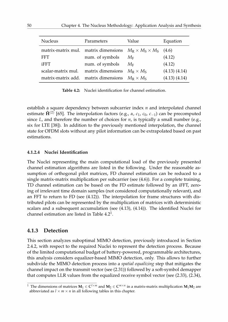
50 Chapter 4. The Nucleus Methodology: Application Analysis and Synthesis
Nucleus Parameters Value Equation
matrix-matrix mul. matrix dimensions MR ×MS ×MS (4.6)FFT num. of symbols MF (4.12)iFFT num. of symbols MF (4.12)scalar-matrix mul. matrix dimensions MR ×MS (4.13) (4.14)matrix-matrix add. matrix dimensions MR ×MS (4.13) (4.14)
Table 4.2: Nuclei identification for channel estimation.
establish a square dependency between subcarrier index n and interpolated channelestimate H(2) [65]. The interpolation factors (e.g., α, c1, c0, c−1) can be precomputedsince L, and therefore the number of choices for n, is typically a small number (e.g.,six for LTE [38]). In addition to the previously mentioned interpolation, the channelstate for OFDM slots without any pilot information can be extrapolated based on pastestimations.
4.1.2.4 Nuclei Identification
The Nuclei representing the main computational load of the previously presentedchannel estimation algorithms are listed in the following. Under the reasonable as-sumption of orthogonal pilot matrices, FD channel estimation can be reduced to asingle matrix-matrix multiplication per subcarrier (see (4.6)). For a complete training,TD channel estimation can be based on the FD estimate followed by an iFFT, zero-ing of irrelevant time domain samples (not considered computationally relevant), andan FFT to return to FD (see (4.12)). The interpolation for frame structures with dis-tributed pilots can be represented by the multiplication of matrices with deterministicscalars and a subsequent accumulation (see (4.13), (4.14)). The identified Nuclei forchannel estimation are listed in Table 4.21.
4.1.3 Detection
This section analyzes suboptimal MIMO detection, previously introduced in Section2.4.2, with respect to the required Nuclei to represent the detection process. Becauseof the limited computational budget of battery-powered, programmable architectures,this analysis considers equalizer-based MIMO detection, only. This allows to furthersubdivide the MIMO detection process into a spatial equalizing step that mitigates thechannel impact on the transmit vector (see (2.31)) followed by a soft-symbol demapperthat computes LLR values from the equalized receive symbol vector (see (2.33), (2.34),
1 The dimensions of matrices M1 ∈ Cl×m and M2 ∈ Cm×n in a matrix-matrix multiplication M1M2 areabbreviated as l ×m× n in all following tables in this chapter.

4.1. Nucleus Analysis: Baseband Receiver for Wireless Communications 51
(2.42), (2.43)). For an efficient implementation of (2.31), first the matched-filter symbolvector
yMF = HHy (4.16)
is calculated by means of a matrix-vector multiplication.2 Next, the Gram matrix
G = HHH (4.17)
is computed, which requires the multiplication of channel matrix estimate H by itsown Hermitian transpose. The symmetry in the occurring inner products allows asignificant reduction of the computational complexity. Since the resulting matrix isHermitian, its lower triangular part equals the mirrored, conjugated upper triangularpart. Then, matrices
Aol =(G + N0IMS
)(4.18)
Ait =(GΛz + N0IMS
). (4.19)
are derived for open-loop (ol) and iterative (it) equalization. Calculating Ait requiresan additional multiplication of G by diagonal matrix Λz which contains the variancesof the remapped symbol vector z. The diagonal addition of N0 is of negligible com-plexity compared to the remaining computations. Next, matrices Aol and Ait have tobe inverted. This presents a major computational effort and a challenge for numericalstability due to the high dynamic range. As a result, Flavors for this Nucleus typ-ically rely on matrix factorization [49, 84] (e.g., QR or LU decomposition). The factthat matrix Aol is hermitian can be used to simplify the matrix inversion in open-loopequalization. The final equalizer step of the open-loop algorithm is performed by onelast matrix-vector multiplication to derive
sol = A−1ol yMF. (4.20)
For iterative equalization, the first step is to perform parallel interference cancellationusing the remapped symbol vector z. This corresponds to a number of scalar-vectormultiply-accumulate operations.
yMF,i = yMF −∑j 6=i
gjzj, i ∈ {1, . . . , MS} (4.21)
The transmit vector is estimated by an unbiased MMSE filter using the column vectorsait,i, i ∈ {1, . . . , MS} of matrix A−1
it . The filter process can be realized by two innerproduct calculations and one scalar inversion.
sit,i =aH
it,i yMF,i
aHit,i gi
(4.22)
2 Since the practical detector implementations in Chapters 4 and 6 operate based on channel matrixestimate H, matrix H in the theoretical detector formulations in Chapter 2 is omitted for H.

52 Chapter 4. The Nucleus Methodology: Application Analysis and Synthesis
After that, the computation scheme for open-loop and iterative detection is the same.The original form of the soft-symbol demapper in (2.33) consists of the product of thepost-equalization SINR ρi and distance term Di,b subject to minimization for the i-thspatial stream and bit label position b.
LPi,b = ρiDi,b (4.23)
Di,b =
mins∈O(−1)
b
|si − s|2 − mins∈O(+1)
b
|si − s|2 (4.24)
Deriving Di,b imposes a high computational burden on embedded systems be-cause it contains a search over the entire alphabet O of constellation symbols. How-ever, typical constellations chosen for IEEE 802.11 [71] wireless LAN or LTE [38] ex-hibit properties that allow to simplify the calculation. The aforementioned standards,for example, both employ Gray mapping [46], depicted in Figure 4.2 for 4-QAM,16-QAM and 64-QAM constellations. Gray mapping means that the labels of neigh-boring constellation symbols vary by one bit, only. This, in turn, also means separategroups of bits encode the inphase and quadrature symbol position. Therefore, thecomplex-valued search in (4.24) can be reduced to two real-valued searches. For theGray-coded 16-QAM constellation in Figure 4.2b, for example, the inphase componentis encoded via the two leftmost bits and the quadrature component is determined bythe rightmost ones. In the real-valued problem formulation, the Euclidean distancecalculation in (2.33) corresponds to subtracting the distances of the equalized symbolcomponent to the closest constellation points with a zero or one at the bit-position ofinterest. This subtraction cancels out the square dependency of the distance on theinphase or quadrature components sI,i = <(si) and sQ,i = =(si). As a result, the cal-culation of the embraced term in (4.24) can be reduced to calculating two (i.e., one forinphase, one for quadrature) piecewise linear functions [112]. The maximum numberof linear subsections depends on the number of bits per constellation symbol and isgiven by 2Q/2 − 1. The functions follow directly from the constellation alphabets, forexample 4-QAM, 16-QAM and 64-QAM as shown in Figure 4.2. They are identicalfor the inphase and quadrature component as well as for the different elements ofthe equalized receive vector. Therefore, the index i is omitted in the following. For4-QAM, (4.24) becomes
D4-QAM1 (sI) = 4sI. (4.25)
For 16-QAM, the piecewise linear function is defined by
D16-QAM1 (sI) =
4sI |sI| ≤ 28(sI − 1) sI > 28(sI + 1) sI < −2
D16-QAM2 (sI) = 8− 4|sI|. (4.26)

4.1. Nucleus Analysis: Baseband Receiver for Wireless Communications 53
I
Q1000
1101
1−1
(a) 4-QAM
I
Q10 1011 1001 1000 10
10 1111 1101 1100 11
10 0111 0101 0100 01
10 0011 0001 0000 00
1 3−1−3
(b) 16-QAM
I
Q
010 010011 010001 010000 010
010 011011 011001 011000 011
010 001011 001001 001000 001
010 000011 000001 000000 000
100 010101 010111 010110 010
100 011101 011111 011110 011
100 001101 001111 001110 001
100 000101 000111 000110 000
010 100011 100001 100000 100
010 101011 101001 101000 101
010 111011 111001 11000 111
010 110011 110001 110000 110
100 100101 100111 100110 100
100 101101 101111 101110 101
100 111101 111111 11110 111
100 110101 110111 110110 110−1 1 3 5 7−3−5−7
(c) 64-QAM
Figure 4.2: Gray-coded constellation alphabets.

54 Chapter 4. The Nucleus Methodology: Application Analysis and Synthesis
For 64-QAM, the respective function is
D64-QAM1 (sI) =
4sI |sI| ≤ 28(sI − 1) 2 < sI ≤ 48(sI + 1) −4 ≤ sI < −212(sI − 2) 4 < sI ≤ 612(sI + 2) −6 ≤ sI < −416(sI − 3) sI > 616(sI + 3) sI < −6
D64-QAM2 (sI) =
8(3− |sI|) |sI| ≤ 24(4− |sI|) 2 < |sI| ≤ 68(5− |sI|) |sI| > 6
D64-QAM3 (sI) =
{4(|sI| − 2) |sI| ≤ 44(6− |sI|) |sI| > 4 .
(4.27)
The last computationally intensive step is to derive the post-equalization SINR. Foropen-loop and iterative detection, the SINR is given by [98]
ρol,i ≈1
N0
[(HHH + N0IMS
)−1]
ii
(4.28)
ρit,i =wH
i hi
1−Λz,iiwHi hi
. (4.29)
Since the term within brackets in the denominator of (4.28) has already been calcu-lated when deriving the equalizer matrix, the remaining computational step is thescalar inversion of the diagonal of the inverted matrix in brackets. For the iterativevariant, the inner product wH
i hi has already been calculated in the denominator of(4.22), so the main computational complexity lies in the scalar inversion. An overviewof the Nuclei identified for MIMO detection is provided by Table 4.3.
4.1.4 Permutation Based Tasks
Tasks like CP removal, subcarrier demapping, pilot extraction, and interleaving/dein-terleaving in the outer modem are mostly based on permutations. As permutationsare no computational tasks, they are also not identified as Nuclei in this context.Regardless, their efficient implementation is important to achieve the timing require-ments of modern communication standards. For some tasks this is straightforward.CP removal, for example, is realized by discarding a number of receive symbols be-fore forwarding the antenna streams to the OFDM demodulator. In a memory-basedsystem, this simply means applying an offset to the base-pointer of the FFT pro-cessing unit. Subcarrier demapping and pilot extraction are more complex to im-

4.1. Nucleus Analysis: Baseband Receiver for Wireless Communications 55
Nucleus Parameters Value Equation
matrix-vector mul. matrix dimensions MS ×MR (4.16)MS ×MS (4.20)
matrix-herm. mul. matrix dimensions MS ×MR ×MS (4.17)matrix-diag. matrix mul. matrix dimensions MS ×MS ×MS (4.19)matrix inversion (herm.) matrix dimensions MS ×MS (4.18)matrix inversion matrix dimensions MS ×MS (4.19)scalar-vector mul.-acc. vector size MS (4.21)inner product vector size MS (4.22)piecewise linear func. linear subsections 2Q/2 − 1 (4.25) (4.26) (4.27)scalar inversion - - (4.22) (4.28)
Table 4.3: Nuclei identification for MIMO detection.
plement because pilots, payload and synchronization symbols are intertwined in astandard and use case specific pattern. A feasible approach is to integrate these twotasks into the addressing of the inputs to detection and channel estimation. Thiscan be done without any penalty regarding timing, if the target platform containsflexible address generation units (AGUs) that can mimic the necessary access pat-terns. Otherwise, there will be an overhead for address calculation in software.Tasks like interleaving, finally, are not suitable for software implementation on mostgeneric, programmable platforms. As interleaving schemes for wireless communica-tion have pseudo-random permutation schemes, a specialized AGU that can gener-ate the standard-specific pseudo-random addresses is necessary [4]. Furthermore, amemory to buffer several hundreds or even thousands of soft-bits may be requiredfor cases where the entire codeword has to be deinterleaved before channel decodingbegins (e.g., when using highly parallel channel decoders).
4.1.5 Channel Decoding
As the focus of this work is on inner modem components, a detailed Nucleus analysisof channel decoding is out of the scope of this work. A study of channel decodingschemes, relevant for modern wireless communication standards, with respect to theircommon computational components has been conducted in [118]. The authors presenta versatile architecture that supports convolutional and turbo decoding for a varietyof communication standards. The resulting 15-stage design with a complex memorysubsystem allowing access to up to six memories in parallel is highly tailored tochannel decoding and can be considered weakly programmable. This underlines theprevious assessment that efficient channel decoding is not suitable for implementationon generic, programmable hardware but requires a tailored architecture instead.

56 Chapter 4. The Nucleus Methodology: Application Analysis and Synthesis
4.1.6 Summary
The preceding sections of this chapter have performed a Nucleus analysis of inner mo-dem algorithms for cellular and wireless LAN communication. To tailor to the com-putational limitations of programmable SDR platforms, detection was constrained toequalizer-based algorithms. The results of the analysis are summarized in Table 4.4.The identified Nuclei come from the domains of Fourier analysis and vector arith-metic. Moreover, a few specialized scalar arithmetic functions are required. Overall,the set of Nuclei is rather small, so the corresponding Flavor libraries can be devel-oped with reasonably low implementation effort. This finding speaks for the validityof the Nucleus methodology and its applicability to digital baseband signal process-ing. The Nuclei in Table 4.4 are to be understood as purely algorithmic constructs.The nature of their Flavors may vary significantly based on the respective target hard-ware architecture. Different number formats and wordwidths in the data path, forexample, may require different degrees of numerical stabilization, particularly fortasks with high dynamic range like matrix inversion.

4.1.Nucleus
Analysis:Baseband
Receiver
forW
irelessC
omm
unications57
Nucleus Parameters Value RX block Equation
FFT num. of symbols MF OFDM mod. (4.2)channel est. (4.12)
iFFT num. of symbols MF OFDM mod. (4.1)channel est. (4.12)
matrix inversion (herm.) matrix dimensions MS ×MS detection (4.18)matrix inversion matrix dimensions MS ×MS detection (4.19)matrix-matrix mul. matrix dimensions MR ×MS ×MS channel est. (4.6)adjoint matrix mul. matrix dimensions MS ×MR ×MS detection (4.17)matrix-diag. matrix mul. matrix dimensions MS ×MS ×MS detection (4.19)matrix-matrix add. matrix dimensions MR ×MS channel est. (4.13) (4.14)matrix-vector mul. matrix dimensions MS ×MR detection (4.16)
MS ×MS detection (4.20)scalar-matrix mul. matrix dimensions MR ×MS channel est. (4.13) (4.14)scalar-vector mul.-acc. vector size MS detection (4.21)inner product vector size MS detection (4.22)piecewise linear func. linear subsections 2Q/2 − 1 detection (4.25) (4.26) (4.27)scalar reciprocal - - detection (4.22) (4.28)
Table 4.4: Nuclei identification: summary for receiver inner modem.

58 Chapter 4. The Nucleus Methodology: Application Analysis and Synthesis
4.2 Target Platforms
This section presents the two target processor cores for the implementation of the in-ner modem functionality analyzed in Section 4.1. The first is the STxP70, an extendibleRISC processor core embedded into the P2012/STHorm platform [10], presented inSection 4.2.1. Section 4.2.2 introduces the second target, the TI TMS320C64x+ [106], awidely used VLIW DSP.
4.2.1 ST Microelectronics P2012
The P2012 [10] (also referred to as STHorm) is a modular many-core computing fab-ric composed of several ENcore compute clusters. Each cluster contains up to 16STxP70 processor cores with private program memories and a shared data mem-ory subsystem. Booting and management of the individual clusters is performed bythe cluster controller (CC). The STxP70 [10] is a RISC-like processor core that canexecute two instructions per cycle (dual issue). It can be equipped with tightly cou-pled extensions [76] at design-time for application specific acceleration. Each coreis programmable in the C programming language, and the functionality added bythe aforementioned extension can be accessed via intrinsics. Additionally, each clus-ter can be extended by stand-alone hardware accelerators called hardware processingelements (HWPEs). Figure 4.3 provides a system level overview of the P2012 platform.
Since the majority of the Nuclei in Table 4.4 come from the domain of vectorarithmetic, the VECx SIMD vector extension provided by ST Microelectronics is aparticularly attractive option for this case study. VECx allows integer operations on128-bit vectors which can be interpreted to contain four, eight, or 16 words of 32, 16,or eight bit. Native fixed-point support is not provided, so there are no shifting unitafter the multipliers to normalize the integer multiplication result to a certain fixed-point format. This limits the efficiency of fixed-point applications in two ways. First,each multiplication has to be followed by an additional explicit right shift to normal-ize the fixed-point result, which reduces the achievable throughput. Second, withouta shifting unit, the wordwidth of the result of a multiplication is the sum of the widthof the two input operands. Thus, when performing SIMD multiplications of 16-bitfixed-point words, the multiplications actually have to be realized using instructionsfor 32-bit integers to avoid overflows. Also, the VECx is tailored to real-valued vec-tor arithmetic, meaning any complex-valued functionality has to be implemented insoftware.
To compare different implementations in terms of area or energy efficiency, it isimportant to characterize the target platform with respect to hardware complexityand energy consumption. Unfortunately, such data is rarely available for commercialplatforms. Therefore, a rough estimate using additional data from other sources hasto be conducted. In 2012, ST Microelectronics presented a tape-out of a version of theP2012 [10] in 28 nm CMOS technology [7] with four ENcore clusters. The STxP70 [10]cores were extended by a single precision floating-point unit. The silicon area per clus-ter was reported as 3.8 mm2. To estimate the area of one processor core, the size of the

4.2. Target Platforms 59
PE 1 PE 2 PE N
ENCore
ENco
reIn
terf
ace
CC
Inte
rfac
e
Local Interconnect
HW HW
Cluster Controller
Fabric
P2012H
WSynchronizer
Controller
PlatformCP
Sub-system
DMASub-
system
Data MemoryShared
Many-CoreComputing Cluster
PE 1 PE 2HWPE K
PM PM PM
Figure 4.3: System level overview of the P2012/STHorm platform [10].
memory subsystem has to be estimated first and subtracted from the above number.The ENcore cluster contains 256 kilobyte (kB) of shared data memory, 17 programmemories of 16 kB each (including the CC) and 32 kB of private data memory for theCC. In total, the resulting memory size is 560 kB. The footprint of the memory systemis estimated based on 28 nm SRAM memory. TSMC reports the integration on 28 nmSRAM cells at 0.127 µm2 per cell [127]. For a functional memory, sense amplifiers andprecharge circuitry have to be considered in addition to the naked SRAM cell. The au-thors of [77] present such a design that provides 4 kbit storage per 1208.4 µm2. Basedon this number, the area footprint of the memory subsystem of the P2012 is estimatedto occupy 1.35 mm2. Since the CC is also based on the STxP70 [10], the remaining areais distributed among 17 cores, leaving 0.144 mm2 per core. Assuming a cell density of85 % (compare Chapter 6) leads to an estimate of 403.6 kGE per core. Since the proces-sor cores in [10] are equipped with a scalar, single precision floating-point unit whichis not relevant for this work, 11.5 kGE are subtracted based on the trial synthesis of a32-bit floating-point multiply-accumulate unit. The VECx extension requires at leastfour additional fixed-point 16-bit multiply-accumulate units and one 32-entry vectorregister file on top of the base core configuration. The multiply-accumulate units re-quire 8.72 kGE for 90 nm CMOS at the scaled clock frequency. The vector register filewith 128-bit words, two read ports and one write port claims additional 33.1 kGE.This brings the total estimated size of the STxP70 [10] core with VECx extension to433.9 kGE. Under heavy load, power consumption is reported at 0.5 mW per clusterat a clock frequency of 600 MHz. Distributing this power among the 16 computa-tional processors and presuming that switching activity approximately scales withhardware complexity, a single STxP70 [10] with VECx is attributed a power consump-tion of 34.3 mW. Table 4.5 summarizes the estimated characteristics, listing hardwarecomplexity AGE, standard cell area A, clock frequency fclk, power consumption P andenergy consumption Eclk per cycle in case of heavy load.

60 Chapter 4. The Nucleus Methodology: Application Analysis and Synthesis
Feature size Vdd [V] A [mm2] AGE [kGE] fclk [MHz] P [mW] Eclk [pJ]
28 nm 1.0 0.155433.9
60034.3
61.590 nm (scaled) 1.0 1.63 187 198
Table 4.5: Estimated characteristics of the STxP70 [10] processor core.
4.2.2 Texas Instruments TMS320C64x+
The TMS320C64x+ [106] (or short C64x+) is a VLIW DSP that is commonly embeddedinto TI integer or fixed-point signal processing platforms like the TMS320C6474 [108].The following section gives an overview of relevant architectural features. The C64x+[106] contains eight functional units that form two data paths A and B. Each data pathcontains the functional units listed below.
• The .M multiplication unit supports an operand wordwidth of 32 bit, but canalso divide 32-bit input words into two 16-bit words or four 8-bit words andperform several multiplications in parallel.
• The .L units mainly performs either additions/subtractions or logic functions.
• The .S unit includes functionality for packing/unpacking data to match differentnumber formats (e.g., sign extension of 8-bit integer words when converted to16-bit words). It also implements arithmetic and logic bit shift operations. Thisprovides a strong advantage over the STxP70 [10] with VECx extension for effi-cient fixed-point processing, since it allows to implement a pipelined fixed-pointmultiply-accumulate operations with full utilization of the .M unit performingthe multiplications, the .L unit performing the additions, and the .S unit per-forming the shift back of the decimal point to its intended position.
• The .D unit is responsible for storing data from the register files to the memoryor loading data from the memory subsystem into one of the register files.
The architecture also incorporates two register files associated with data paths A and Brespectively, even though the functional units can also load (at most) one operand perclock cycle from their non-associated register file. Figure 4.4 shows a simplified high-level perspective of the C64x+ [106] DSP core. The initial stages fetch and dispatch aninstruction word which is then decoded by the respective data path where it definesthe external configuration of the aforementioned functional units. The functionalunits are not aligned sequentially in a certain order to form a pipeline. Instead,they are arranged in parallel so all units can be active at the same time. Since eachfunctional unit has its own read and write ports to the register file, a processingpipeline can be formed dynamically at runtime where the register file takes the roleof the pipeline register. While the additional access ports to the register files cause an

4.3. Algorithmic Design Space 61
.L1
.S1
.M1
.D1
Reg
iste
rFi
leA
from Register File BIn
stru
ctio
nD
ecod
e
16/3
2Bi
tIn
str.
Dis
patc
h
Inst
ruct
ion
Fetc
h
Figure 4.4: Overview of the TI C64x+ [106] DSP architecture.
Feature size Vdd [V] A [mm2] AGE [kGE] fclk [MHz] P [mW] Eclk [pJ]
65 nm 1.2 - - 1200 660 55090 nm (scaled) 1.0 1.98
688867 458 529
130 nm 1.2 4.14 600 - -
Table 4.6: Estimated characteristics of the TI C64x+ [106] DSP.
overhead with respect to hardware complexity, they also provide more flexibility toform many types of processing pipelines.
A detailed description of an implementation of the C64x+ in 130 nm CMOS tech-nology is provided by [2]. The silicon complexity is listed as 64 million transistors,including hardware accelerators and the entire memory subsystem. The C64x+ coreitself makes up a fraction of around 4.31 % of the total chip area, which puts it at ap-proximately 2.76 million transistors or 689 kGE. The design achieves a clock frequencyof 600 MHz while consuming 718 mW of power. Unfortunately, authors in [2] do notlist an exact power breakdown of the on-chip components, so the power breakdownis taken from the TMS320C6474 implementation in 65 nm technology. TI list a typ-ical power consumption of 6 W for the entire 3-core platform including peripherals,where each core is attributed a share of 11 % of the total power consumption [105].This results in a power consumption of 660 mW per core and an energy consumptionof 550 pJ per cycle when running at the maximum clock frequency of 1.2 GHz. Theestimated performance data of of the C64x+ [106] core is summarized in Table 4.6.
4.3 Algorithmic Design Space
The Flavors corresponding to the Nuclei in Table 4.4 do not necessarily mimic thecomputation scheme of the initial form of the Nucleus description. This section

62 Chapter 4. The Nucleus Methodology: Application Analysis and Synthesis
describes a series of algorithmic transformations applied to the purely algorithmic,Nuclei-based application description presented in Section 4.1. These transformationsare either motivated by the reduction of computational complexity or by the need foradditional numerical stability.
4.3.1 Equalizer
The matrix inversion involved in the equalization of the MIMO receive symbol vectorsmay require numerical stabilization (e.g., based on matrix factorization) depending onthe wordwidth and number format of the data path on the target processor. The fol-lowing paragraphs analyze different factorization/inversion schemes (i.e., LU, DnQ,LDLh, QR [1, 45, 92, 122]) along with further miscellaneous vector arithmetic opera-tions required for equalization with respect to their computational complexity. Forthis analysis, computational complexity is evaluated on the granularity of the follow-ing scalar operations:
• cmul: Complex-valued scalar multiplication.
• cadd: Complex-valued scalar addition.
• rsqrt: Reciprocal real-valued square root.
• sqrt: Real-valued square root.
• rsca: Reciprocal of real-valued scalar value.
To keep the set of elementary operations small, multiplications and additions involv-ing real-valued operands are also counted as complex-valued. This section only liststhe computational complexity results. The interested reader is referred to AppendixA for a detailed complexity derivation.
4.3.1.1 Triangular Matrix Inversion
Some factorization schemes (e.g., LU) require the inversion of a triangular matrix, sothe complexity of this operation is discussed up-front here. Without loss of generality,the complexity is derived for a lower triangular matrix L ∈ Cn×n. The diagonal entriesof L−1 are computed directly from the diagonal of L.
L−1ii =
1Lii
(4.30)
The off-diagonal elements are derived by back-substitution according to
L−1ij = −
i−1∑k=j
L−1kj
LiiLik. (4.31)
It is assumed that the reciprocal of a complex-valued number x (e.g., in (4.30)) iscomputed by first expanding the fraction 1/x by the complex conjugate of x, com-puting the reciprocal of the real-valued denominator (i.e., |x|2) and multiplying the

4.3. Algorithmic Design Space 63
result by the conjugate of x. Therefore, one complex-valued reciprocal is mappedonto two complex-valued multiplications and one real-valued reciprocal. The overallcomputational complexity of (4.30) and (4.31) is given by
Ncmul =n3 + 5n
3(4.32)
Ncadd =n3 − 3n2 + 2n
6(4.33)
Nrsca = n. (4.34)
4.3.1.2 Triangular Matrix Inversion with Unity Diagonal
In some cases (e.g., Section 4.3.1.4), the triangular matrix to invert has a unity diago-nal. This results in a reduced computational complexity compared to Section 4.3.1.1.
Ncmul = Ncadd =n3 − 3n2 + 2n
6(4.35)
4.3.1.3 Triangular Matrix-Vector Multiplication
Equalization based on certain factorizations (e.g., LU) contains the multiplication ofthe matched-filtered receive vector by a series of triangular matrices. The complexityof the multiplication of a triangular matrix M ∈ Cn×n by a vector v ∈ Cn×1 is
Ncmul =n∑
i=1
i =n(n + 1)
2(4.36)
Ncadd =n−1∑i=1
i =(n− 1)n
2. (4.37)
4.3.1.4 LU Factorization
By applying LU factorization, a matrix A ∈ Cn×n is rewritten as the product
A = LU (4.38)
of lower triangular matrix L ∈ Cn×n with unity diagonal and upper triangular matrixU ∈ Cn×n [45]. Based on this decomposition, the inversion of A is given by
A−1 = U−1L−1, (4.39)
which is the matrix algebra equivalent of Gaussian elimination. Matrices L and Ucan be computed by the computation scheme in Algorithm 1 [45]. Both matrices areembedded into the result matrix M ∈ Cn×n and can be extracted from its lower andupper triangular parts, where the diagonal of M belongs to U. The computational

64 Chapter 4. The Nucleus Methodology: Application Analysis and Synthesis
Algorithm 1 LU factorization computation scheme [45].1: M← A2: for k = 1 to n− 1 do3: for i = k + 1 to n do4: Mik = Mik/Mkk5: end for6: for i = k + 1 to n do7: for j = k + 1 to n do8: Mij ← Mij −Mik Mkj9: end for
10: end for11: end for
complexity of Algorithm 1 is given by
Ncmul =n3 + 5n− 6
3
Ncadd =2n3 − 3n2 + n
6Nrsca = n− 1. (4.40)
4.3.1.5 Divide and Conquer (DnQ)
A divide and conquer (DnQ) approach solves a bigger problem by decomposing it intoa set of smaller problems that are solved independently and then combined to derivethe final result. In the following, the inversion of matrix A ∈ C2×2 is defined as oneof these sub-problems. The direct form of the inversion of A is given by
A−1 =1
det A
(+a22 −a12
−a21 +a11
), (4.41)
with determinant det A = a11a22− a12a21. Based on (4.41), bigger size matrices can beinverted in divide and conquer fashion [1], for example matrix M ∈ C4×4 composedof submatrices A, B, C, D ∈ C2×2.
M =
(A B
C D
)(4.42)
The inverse of M can be written entirely based on matrices A, B, C, D [1] accordingto
M−1 =
(A−1 + A−1BSCA−1 −A−1BS
−SCA−1 S
)(4.43)
with Schur complementS = (D− CA−1B)−1. (4.44)

4.3. Algorithmic Design Space 65
The application of (4.43) and (4.44) is not limited to 4× 4 matrices but may be ap-plied to any partitioned matrix as in (4.42). However, this section discusses the 4× 4case due to its relevance for IEEE 802.11n [69] MIMO detection. The computationalcomplexity of the 2× 2 inversion algorithm in (4.41) is given by
N2×2cmul = 8, N2×2
cadd = 1, N2×2rsca = 1. (4.45)
In the granularity of 2 × 2 operations, the 4 × 4 algorithm requires two matrix in-versions, six matrix multiplications, and two matrix additions. The matrix multi-plications are composed of eight scalar multiplications and four additions. Matrixadditions, finally, require four scalar additions. Combining these complexities, theoverall computational effort of the 4× 4 inversion is given by
N4×4cmul = 64, N4×4
cadd = 34, N4×4rsca = 2. (4.46)
If only used for the inversion of hermitian matrices, the complexity in (4.46) can bereduced further (e.g., exploiting B = CH).
4.3.1.6 LDLh Factorization
The LDLh algorithm factorizes a square, positive semi-definite matrix A ∈ Cn×n intothe product
A = LDLH, (4.47)
where L is a lower triangular matrix with a unity diagonal and D is a diagonal matrix[122]. The inverse of A is calculated according to
A−1 = L−HD−1L−1. (4.48)
Due to the diagonal/triagonal structure of D and L, these inversions are less compu-tationally complex. Matrix D−1 is calculated by the element-wise scalar reciprocal ofthe diagonal elements of D, and matrix L−1 can be derived via back substitution. Theelements of D are defined by
Djj = Ajj −j−1∑k=1
∣∣Ljk∣∣2 Dkk. (4.49)
The diagonal elements of the lower triangular matrix L are initialized by Ljj = 1. Thesubdiagonal elements are calculated according to
Lij =1
Djj
Aij −j−1∑k=1
LikDkkLHjk
for i > j . (4.50)

66 Chapter 4. The Nucleus Methodology: Application Analysis and Synthesis
The computation of (4.49) and (4.50) requires a total of
Ncmul =n3 + 6n2 − n
6(4.51)
Ncadd =n3 − n
6(4.52)
Nrsca = n (4.53)
complex-valued multiplications, additions, and real-valued scalar reciprocals.
4.3.1.7 Modified Gram-Schmidt QR Factorization
QR factorization rewrites a matrix A ∈ Cm×n as the product of unitary matrix Q ∈Cm×n and upper triangular matrix R ∈ Cn×n. Two common choices for hardwareimplementation are the modified Gram-Schmidt (MGS) and the Givens rotation (GR)scheme [92, 122]. The MGS scheme derives Q from the input matrix by a series ofcolumn-wise vector projections and subtractions that eliminate inter-column lineardependencies. Since it operates exclusively on vectors of the same size, this schemeis particularly well suited for SIMD architectures. However, the series of projectionsand subtractions can be numerically critical by exceeding the numeric range of nar-row fixed-point formats, which makes further stabilization necessary. GR, on theother hand, employs norm-preserving vector rotations, so it is less critical with re-spect to numerical stability. Executing these rotations requires trigonometric func-tions, though. Unless the target platform contains hardware accelerators for thesefunctions, GR is not well suited for programmable solutions. For the STxP70 [10],for example, 4× 4 QR factorization by GR has a 68 % execution time overhead as op-posed to a stabilized MGS factorization [51]. For ASIC implementations on the otherhand, the opposite result is obtained. The authors of [84] present a GR-based QRfactorization ASIC that employs CORDIC rotations to efficiently implement trigono-metric functions. The resulting GR implementation is 69 % more area-efficient thanthe corresponding MGS implementation.
The computational scheme of the MGS algorithm is shown in Algorithm 2. Thealgorithm starts by computing norms ξi, i ∈ {1, . . . , n} of all n column vectors. Then,it iterates from left to right through the column vectors of the input matrix, normalizesthe current column vector and finally projects it onto all adjacent column vectors andsubtracts the result of the projection from the right-hand vector to generate a set oforthonormal column vectors. The resulting computational complexity is
Ncmul = mn2 + 2mn +n2 − n
2Ncadd = mn2
Nsqrt = nNrsca = n. (4.54)

4.3. Algorithmic Design Space 67
Algorithm 2 Modified Gram-Schmidt (MGS) QR factorization.1: Q← A2: for i = 1 to n do3: ξi =
(AHA
)ii
4: end for5: for i = 1 to n do6: Rii =
√ξi
7: qi ← qi/Rii8: for j = i + 1 to n do9: Rij ← qH
i qj10: qj ← qj − Rij qi11: ξ j ← ξ j − |Rij|212: end for13: end for
4.3.1.8 Comparison
The following compares the computational complexity of open-loop linear MIMOequalization including equalizer matrix calculation using the LU, LDLh, DnQ, and QRalgorithms. Table 4.7 lists the vector arithmetic operations involved in equalization.The LU, LDLh and DnQ algorithms have to compute matrix Aol from (4.18). Thus,they all require one multiplication of the channel matrix with its adjoint version andthe addition of the noise spectral density on the resulting matrix diagonal. Usinga regularized QR factorization (see Section 4.4.1.1) allows to circumvent these twopreprocessing steps. LU, LDLh and DnQ also require the matched filter receive vectoryMF derived from a matrix-vector multiplication. For LU and LDLh factorization, thefactor matrices L, U and D have to be inverted. The inversions of both matricesL can be simplified as they both have a unity diagonal. To complete equalization,the inverted matrices have to be multiplied by the matched filter receive vector. ForLU factorization, this requires two multiplications of a triangular matrix by a vector,where one of the matrices has a unity diagonal. For the LDLh algorithm, two ofthe three factor matrices are triangular with unity diagonal, and the third matrix isdiagonal. As the inverse of diagonal matrix D is already calculated within the LDLhfactorization, the inversion is not listed again in Table 4.7. Since the DnQ variantcomputes A−1
ol without factorization, equalization is finished by multiplying A−1ol by
matched filter vector yMF. For QR factorization, neither Q nor R have to be inverted,since Q is unitary and R−1 is inherently calculated by the regularized QR factorizationalgorithm. Therefore, equalization is finished by two matrix-vector multiplications,whereof one matrix is triangular.
Table 4.8 shows the resulting scalar operation counts. LDLh and QR factorizationare both only applicable for the inversion of hermitian matrices. This specializationshould deliver a reduced complexity compared to the LU and DnQ algorithm whichare applicable to any matrix of full rank. However, this expectation is only fulfilled bythe LDLh algorithm that has the overall lowest computational complexity. QR-based

68 Chapter 4. The Nucleus Methodology: Application Analysis and Synthesis
LU LDLh DnQ QR
adjoint matrix mul. 1 1 1 0matrix-diag. matrix add. 1 1 1 0matrix factorization 1 1 - 1triag. matrix inversion 1 0 0 0triag. matrix inversion (unity diag.) 1 1 0 0matrix-vector mul. 1 1 2 1triag. matrix-vector mul. 1 0 0 1triag. matrix-vector mul. (unity diag.) 1 2 0 0diag. matrix-vector mul. 0 1 0 0
Table 4.7: Computational complexity of open-loop MIMO equalization in granular-ity of vector arithmetic operations using LU, LDLh, DnQ, and QR basedmatrix inversion.
2× 2 4× 4
LU DnQ LDLh QR LU DnQ LDLh QR
cmul 24 22 19 40 130 136 102 224cadd 9 10 8 19 77 92 66 146rsca 3 1 2 2 7 2 4 4rsqrt 0 0 0 0 0 0 0 0sqrt 0 0 0 2 0 0 0 4
Table 4.8: Computational complexity of 2× 2 and 4× 4 open-loop MIMO equalizerin granularity of scalar operations.
equalization, on the other hand, has the overall highest computational complexity.As a compensation, QR factorization exhibits the lowest numerical precision require-ments of all presented alternatives [49]. The computational complexities of LU andDnQ based equalization are close to identical with a slight advantage of LU for the4× 4 case.
Based on scalar operation count, LDLh should be chosen for open-loop equaliza-tion and LU for the iterative variant. This conclusion may be valid for an ASIC that canbe designed to match the structure of the algorithm at hand, but for implementationon an existing programmable processor core, the match between algorithm and archi-tecture has to be considered as well. LU and LDLh factorization operate on vectorsof varying size, so their implementation on a vectorial SIMD processor (see Section

4.3. Algorithmic Design Space 69
2-2-4 4
sI
-24
-16
8
16
24 D16-QAM1
-8
(a) First soft-bit.
2-2-4 4
sI
-24
-16
8
16
24 D16-QAM2
-8
(b) Second soft-bit.
Figure 4.5: Soft-symbol demapping for 16-QAM.
5.2.1) like the STxP70 [10] will result in underutilization of the data path. DnQ, onthe other hand, operates on fixed size vectors and matrices. Thus, it lends itself wellto implementation on vectorial SIMD architectures, as long as their number formatprovides a sufficient range for the direct matrix inversion in (4.41) (see Chapter 5).The narrow wordwidth fixed-point architectures considered in this chapter call forthe numerically more stable QR-based equalization.
4.3.2 Soft-Symbol Demapper
For Gray-coded constellations alphabets, soft-symbol demapping reduces to the cal-culation of a constellation dependent, piecewise linear function for the inphase andquadrature components of each equalized symbol (see Section 4.1.3). A piecewiselinear function is characterized by its subsections and their respective slopes and in-tercepts. For maximum flexibility, an implementation parametrized by the characteri-zation of an arbitrary piecewise linear function is desirable. This function then couldbe used in the LLR calculation for any constellation. Unfortunately, the input rangechecks and conditional statements in (4.26) and (4.27) do not lend themselves well tosoftware implementation due to potential jumps and pipeline flushes. Instead, the ex-pressions for 16-QAM and 64-QAM are transformed to a continuous expression. For64-QAM, this step involves an additional approximation to make the piecewise linearfunction more manageable. The 4-QAM demapping function, on the other hand, isalready continuous and requires no further simplification.
The 16-QAM demapping function according to (4.26) is illustrated in Figure 4.5.The second soft-bit is already in a form that can be computed by any processor thatcan calculate absolute values. As previously shown in the scope of this work [52], thefirst soft-bit can be constructed from the second one by clipping all values below zero,

70 Chapter 4. The Nucleus Methodology: Application Analysis and Synthesis
2-2-4 4
-16
81624
-8
-24
324048
-32-40-48
6 8
52
-52
-6-8sI
D64-QAM1
(a) First soft-bit.
2-2-4 4
-16
81624
-8
-24
324048
-32-40-48
6 8
52
-52
-6-8sI
D64-QAM2
(b) Second soft-bit.
2-2-4 4
-16
81624
-8
-24
324048
-32-40-48
6 8
52
-52
-6-8sI
D64-QAM3
Approx.Exact
(c) Third soft-bit.
Figure 4.6: Soft-symbol demapping for 64-QAM.
multiplying the result by sign(sI) and adding the result to a linear function with anintersect of zero and a slope of four according to
D16-QAM1 (sI) = sign(sI) ·max
{0, D16-QAM
2 (sI)}+ 4 sI. (4.55)
Since most DSPs have an instruction for maximum and sign calculation, (4.55) is morehardware friendly than (4.26).
The authors of [112] propose a hardware-friendly approximation of 64-QAM soft-symbol demapping as in (4.27) that is described in the following. To illustrate thereasoning behind this approximation, Figure 4.6 shows the exact demapping func-tions in solid black and the approximated functions in dashed red lines. The strictlyincreasing demapping function of the first soft-bit as in Figure 4.6a is approximatedby extending the linear segment for |sI| ≤ 2 to the entire range of sI. The zigzaggedtriangular shape of the second soft-bit is simplified to a straight triangular function(see Figure 4.6b). For the third soft-bit illustrated in Figure 4.6c, the authors of [112]propose no additional approximation. In addition to the approximations in [112], thethird soft-bit can be constructed from the approximation of the second one by takingthe negative of its absolute value and shifting it up by eight units. The resulting,simplified demapping functions are given by
D64-QAM1 (sI) ≈ 4 sI
D64-QAM2 (sI) ≈ −|sI|+ 16
D64-QAM3 (sI) ≈ −|D64-QAM
2 (sI)|+ 8. (4.56)

4.4. Application Synthesis 71
Since the approximated demapping functions in (4.56) are continuously formulated,they are suited for a hardware-friendly implementation. Simulations conducted within[112] and this work did not show any notable performance degradation using afore-mentioned approximation.
4.4 Application Synthesis
Following the platform-independent Nuclei identification in Section 4.1, this sectionpresents practical implementation results of mapping the analyzed application ontothe two target processor cores introduced in Section 4.2. After some algorithmic trans-formations for improved numerical stability in Section 4.4.1, benchmarked Flavor im-plementations are discussed in Section 4.4.2. The target application is then synthe-sized using these Flavors. Synthesis results are listed Section 4.4.3.
4.4.1 Adaptations for Narrow Wordwidth
To enable the use of 16-bit fixed-point data formats on the STxP70 [10] and C64x+[106] target processor cores, MGS QR factorization is used to circumvent a directmatrix inversion in the equalizer. On the one hand, this algorithm exhibits the highestcomputational complexity in terms of scalar operation count of the equalizer variantscompared in Table 4.8. On the other hand, it works strictly on fixed-size columnvectors of the input matrix and therefore it is well suited for implementation on aSIMD processor core. Also, it has shown to be numerically stable with the narrowestwordwidth of all compared algorithms [49]. Section 4.4.1.1 provides more details onthe use of the QR factorization for open-loop equalization. Section 4.4.1.2 does thesame for iterative equalization. In Section 4.4.1.3, further modification for operationon narrow wordwidth number formats are introduced.
4.4.1.1 Open-loop Equalization by Regularized QR Factorization
The following describes the inversion of a hermitian matrix by means QR factorizationand uses the result to calculate equalizer matrix WH
ol from (2.32). Every hermitianmatrix M ∈ CN×N can be written as
M = AHA + aIN (4.57)
for A ∈ CM×N with M, N ∈N and a ∈ R [45]. Augmenting A to form matrix
A =
[A√
a IN
]∈ C(M+N)×N (4.58)
allows to rewrite the inversion of M based on the QR factorization A = QR [128]which is referred to as a regularized QR factorization. Here, Q ∈ C(M+N)×N is a

72 Chapter 4. The Nucleus Methodology: Application Analysis and Synthesis
unitary matrix and R ∈ CN×N is an upper triangular matrix. The inverse of M is thengiven by
M−1 =(
AHA)−1
=(
RHQHQR)−1
= R−1R−H. (4.59)
Partitioning Q into matrices Q1 ∈ CM×N and Q2 ∈ CN×N [128] so that[A√
a IN
]=
[Q1
Q2
]R (4.60)
reveals that [128]
R−1 =Q2√
a. (4.61)
Therefore, the triangular matrix inversion in (4.59) can be avoided by reformulating
M−1 =Q2QH
2a
. (4.62)
For open-loop equalization, computational complexity can be reduced by using equal-izer matrix WH
ol directly instead of deriving matched filtered receive vector yMF andthen applying the matched filter equalizer matrix A−1
ol . Matrix WHol can be represented
by (4.62) choosing A = H and a = N0. In that case, H = Q1R. With that, it followsthat
WHol = M−1HH =
Q2QH1√
N0. (4.63)
Based on (4.63), open-loop equalization can be reduced to a regularized QR factoriza-tion followed by two matrix-vector multiplications, given there is sufficient memoryto store Q2 and QH
1 . Otherwise, WHol can be computed up-front and then be used to
equalize receive vector y directly.
4.4.1.2 Iterative Equalization by QR Factorization
For a regular matrix M ∈ CN×N that is not necessarily hermitian (e.g., Ait in (4.19)),QR factorization can also be used to reduce the dynamic range of matrix inversion.By factorizing M = QR with unitary matrix Q ∈ CN×N and upper triangular matrixR ∈ CN×N, it follows that
M−1 = R−1QH. (4.64)
In this formulation, the inverse of R has to be calculated explicitly. For iterativeequalization, M is set to Ait and the calculation proceeds according to (4.22).
4.4.1.3 Stabilized Modified Gram-Schmidt QR Factorization
The MGS QR factorization scheme from Algorithm 2 is now extended further foradditional numerical stability. The stabilization measures are shown in Algorithm 3.First, it is assumed that a =
√N0 and b ∈ R(MR+MS)×1 is a vector with all entries

4.4. Application Synthesis 73
Algorithm 3 Regularized MGS QRD with dynamic scaling and IACM [51].
1: Q←[HT;
(a IMS
)T]T
2: for i = 1 to MS do3: ξi =
(HHH
)ii + N0
4: end for5: for i = 1 to MS do6: for j = i to MS do7: if max{|<{qj[1]}|, |={qj[1]}|, ..} < TL then8: qj ← 2qj9: ξ j ← 4 · ξ j
10: else if max{|<{qj(1)}|, |={qj(1)}|, ..} > TH then11: qj ← qj/212: ξ j ← 1/4 · ξ j13: end if14: end for15: qi ← qi/
√ξi
16: for j = i + 1 to MS do17: s = (b ◦ qi)
H (b ◦ qj)
18: qj ← qj − s qi19: ξ j ← ξ j − |s|220: end for21: end for
equal one. The Hadamard operator ◦ denotes element wise multiplication. Matrix Qin Line 1 is initialized with the augmented channel matrix and contains [QT
1 QT2 ]
T afterprocessing is finished. For Q to be unitary, its column vectors have to be normalizedto unity. To that end, column norms of Q are precalculated in Line 3 and updatedin Line 19 after every projection and subtraction. The core part of the algorithm islocated in Lines 15 to 20. The algorithm proceeds column-wise from left to right,normalizes the leftmost column, projects it onto all right-hand column vectors andsubtracts the projected vectors. Afterwards, the algorithm repeats the same schemefrom the next column vector to the right until all columns have been normalizedand the resulting matrix Q is unitary. Line 6 to 14 implement column-wise dynamicscaling [81]. Dynamic scaling operates on entire column vectors and starts by findingthe maximum absolute value of all real/imaginary parts of each element within thecurrent vector. In case this value is above a certain threshold TH, a bitwise arithmeticright shift of all elements is executed. If it is below the lower threshold TL, a left shiftis performed. Since Algorithm 3 tracks the column vector norms of Q, norms ξi haveto be updated after each shift.
Within the scope of this work [51], it was shown that linear detection based onAlgorithm 3 with dynamic scaling still becomes numerically unstable for the high-SNR regime for processing on a typical 16-bit system. The reason is that for high SNR,N0 becomes small and therefore only a small amount of LSBs are used to calculate Q2.

74 Chapter 4. The Nucleus Methodology: Application Analysis and Synthesis
As a result, the equalizer matrix in (4.63) itself becomes instable. This problem canbe circumvented by using an identity augmented channel matrix (IACM) [51], a channelmatrix augmented by an identity matrix instead of an identity matrix scaled by
√N0,
as input matrix to the regularized QR factorization. In response, the inner productcalculation in Line 17 has to be adapted to scale the last MS elements of qi and qj by√
N0, thus setting
a = 1 (4.65)
bi =
{1 i ≤ MR√
N0 i > MR.(4.66)
All QR factorization based equalizer implementations listed in the remainder of thischapter apply dynamic scaling as well as IACM.
4.4.2 Flavor Implementation
Table 4.9 provides an overview of the Flavors corresponding to the Nuclei presentedin Table 4.4 and the algorithmic transformations described in Section 4.3. Target pro-cessor cores are the previously introduced STxP70 [10] by ST Microelectronics andthe C64x+ [106] DSP by TI. The results for the STxP70 [10] are partly based on aninitial implementation developed in the scope of the author’s earlier work [48]. Forthe TI C64x+ [106] DSP, Flavors for FFT, iFFT, 4× 4 matrix-matrix multiplication, andreciprocal calculation are taken from the DSP library [104] provided by TI. All otherFlavors were developed exclusively in the scope of this work. Table 4.9 compares cy-cle count Cexe and execution time Texe as well as estimated energy consumption Eexeand hardware efficiency ηH for the relevant Flavors on both processors. Estimates Eexeand ηH are based on the cycle counts derived from cycle accurate simulation modelsand the cycle based efficiency metrics presented in Table 4.5 and 4.6. Technology de-pendent results are scaled to 90 nm feature size and 1 V supply voltage to enable afair comparison between the STxP70 [10] and the C64x+ [106] processor cores.
Regarding hardware efficiency, it turns out that the C64x+ [106] delivers superiorperformance for all investigated Flavors. This finding renders the STxP70 [10] unsuit-able for the more computationally complex iterative equalizer-based detection, whichis also the reason why the corresponding Flavors for iterative detection were imple-mented only on the C64x+ [106]. The efficiency gap can be explained by the moregeneric nature of the STxP70 [10] that comprises a dual issue RISC pipeline, while theFlavors in Table 4.9 mostly rely on the vector extension. In terms of energy efficiency,on the other hand, the STxP70 [10] performs similar or even superior.
Some interesting conclusions can be be drawn regarding the suitability of each ar-chitecture for different Flavors based on how the ratio of both processors’ efficiencieschange from Flavor to Flavor. The hardware efficiency advantage of the C64x+ [106]is most significant for the FFT/iFFT operation. Even though the FFT implementationon the STxP70 [10] can be vectorized to a certain extend [48] by exploiting the SIMDarchitecture, the C64x+ [106] offers special instructions that facilitate an efficient FFT
4.4. Application Synthesis 75
processing (e.g., for permutation, simultaneous addition and subtraction). The hard-ware efficiency gap between the two processors is smallest for Flavors based on vectorarithmetic using vectors with four elements. This effect can be observed clearly forthe regularized MGS QR factorization. For the 4× 4 variant, the hardware and energyefficiency ratios of the STxP70 [10] over the C64x+ [106] are 0.48 and 3.7, respectively,which are two of the highest ratios observed for all Flavors. Accordingly, the 4-waySIMD STxP70 [10] performs best when the size of the vectors involved in the Flavorcorresponds to the SIMD parallelism. In comparison, the ratios shrink to 0.23 and 1.8for the 2× 2 variant of the same Flavor. This raises the question of the versatility ofSIMD architectures for vector arithmetic tasks and their suitability for flexible SDR so-lutions. This issue will be discussed in-depth in Section 5.2, which presents differentdesign choices for SIMD architectures. These choices ultimately relate to positioningthe design somewhere along the efficiency-flexibility trade-off.
Note that the STxP70 [10] with VECx vector extension does not place itself clearlyon that scale. On the one hand, much needed hardware support for efficient digitalsignal processing is lacking (e.g., native fixed-point arithmetic or support for complex-valued computations). On the other hand, certain important measures for flexibilitywere not taken. Most notable are shortcomings in the memory subsystem. The 4-waySIMD capabilities could have been used for a fourfold parallelization of typical scalarprocessing instead of using it for vector arithmetic only. Unfortunately, though, thememory subsystem does not provide the means to efficiently load and store non-adjacent data in parallel. As a result, the vector data path is only suitable for op-erations on vectors of four adjacent scalars. For all other cases, it is underutilized,which explains why the STxP70 [10] falls short in terms of hardware efficiency whencompared to the TI C64x+ [106].
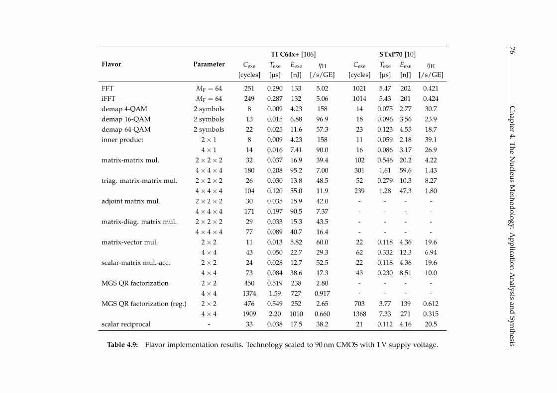
76C
hapter4.T
heN
ucleusM
ethodology:Application
Analysis
andSynthesis
Flavor ParameterTI C64x+ [106] STxP70 [10]
Cexe Texe Eexe ηH Cexe Texe Eexe ηH
[cycles] [µs] [nJ] [/s/GE] [cycles] [µs] [nJ] [/s/GE]
FFT MF = 64 251 0.290 133 5.02 1021 5.47 202 0.421iFFT MF = 64 249 0.287 132 5.06 1014 5.43 201 0.424demap 4-QAM 2 symbols 8 0.009 4.23 158 14 0.075 2.77 30.7demap 16-QAM 2 symbols 13 0.015 6.88 96.9 18 0.096 3.56 23.9demap 64-QAM 2 symbols 22 0.025 11.6 57.3 23 0.123 4.55 18.7inner product 2× 1 8 0.009 4.23 158 11 0.059 2.18 39.1
4× 1 14 0.016 7.41 90.0 16 0.086 3.17 26.9matrix-matrix mul. 2× 2× 2 32 0.037 16.9 39.4 102 0.546 20.2 4.22
4× 4× 4 180 0.208 95.2 7.00 301 1.61 59.6 1.43triag. matrix-matrix mul. 2× 2× 2 26 0.030 13.8 48.5 52 0.279 10.3 8.27
4× 4× 4 104 0.120 55.0 11.9 239 1.28 47.3 1.80adjoint matrix mul. 2× 2× 2 30 0.035 15.9 42.0 - - - -
4× 4× 4 171 0.197 90.5 7.37 - - - -matrix-diag. matrix mul. 2× 2× 2 29 0.033 15.3 43.5 - - - -
4× 4× 4 77 0.089 40.7 16.4 - - - -matrix-vector mul. 2× 2 11 0.013 5.82 60.0 22 0.118 4.36 19.6
4× 4 43 0.050 22.7 29.3 62 0.332 12.3 6.94scalar-matrix mul.-acc. 2× 2 24 0.028 12.7 52.5 22 0.118 4.36 19.6
4× 4 73 0.084 38.6 17.3 43 0.230 8.51 10.0MGS QR factorization 2× 2 450 0.519 238 2.80 - - - -
4× 4 1374 1.59 727 0.917 - - - -MGS QR factorization (reg.) 2× 2 476 0.549 252 2.65 703 3.77 139 0.612
4× 4 1909 2.20 1010 0.660 1368 7.33 271 0.315scalar reciprocal - 33 0.038 17.5 38.2 21 0.112 4.16 20.5
Table 4.9: Flavor implementation results. Technology scaled to 90 nm CMOS with 1 V supply voltage.

4.4. Application Synthesis 77
4.4.3 Application Benchmark
This section discusses application synthesis, composing the target application of theFlavors presented in Section 4.4.2. This synthesis serves as a proof-of-concept for theNucleus methodology and allows to assess its efficiency. Once again, the STxP70 [10]with VECx vector extension and the TI C64x+ [106] DSP are used as target processors.Both processors employ the same frame code but use their own individual Flavorlibraries. It is the aim of this section to show that the main computational effortlies within the previously identified Flavors, while the impact of the frame code orany miscellaneous operations is negligible. Since it exhibits the highest computationalcomplexity of all inner modem tasks discussed in this chapter, this section presents theaforementioned synthesis for equalizer-based MIMO detection for a 2× 2 and 4× 4antenna setup. The comparison is performed for the open-loop variant, since iterativedetection is not implemented on the STxP70 [10] due to throughput limitations.
The upper part of Table 4.10 lists the theoretical per-subcarrier execution timesfor 2× 2 and 4× 4 open-loop linear MIMO detection based on the identified Flavors.The lower part lists the execution time of the entire detection application includingall overheads (e.g., control structures in the frame code). The open-loop algorithmcan be divided into a preprocessing part that computes the equalizer matrix, and adetection part that equalizes the receive vector using this matrix and then performssoft-symbol demapping on the equalized vector. Table 4.10 list the execution timefor 64-QAM soft-symbol demapping, since 64-QAM is the densest constellation in theIEEE 802.11n [69] standard with the most computationally complex demapping. If thewireless channel can be assumed to be constant for the duration of one frame, whichis usually the case for indoor wireless LAN communication (see Section 2.2.1), theequalizer matrices have to be computed only once per subcarrier and can be reusedduring the entire frame.
The execution times in Table 4.10 were obtained from an exemplary transmissionof one IEEE 802.11n [69] PHY layer frame with eight data slots. The correspondinginformation payload is 4.1 kbit for the 2× 2 setup and 8.1 kbit for the 4× 4 variant fora 5/6 code rate. The Flavor density, i.e., the fraction of the total execution time spentexecuting the listed Flavors in relation to the overall execution time, is over 90 % forall antenna setups on both platforms. This means that an optimized Flavor libraryguarantees short execution times and an efficient target application. Also, the Flavorlibrary for inner modem processing presented in Table 4.9 only contains a manageableset of Flavors. Therefore, the overall implementation effort is limited as well, whichallows a fast migration from one target platform to another (e.g., from the STxP70 [10]to the C64x+ [106]).
To be IEEE 802.11n [69] real-time capable, each core has to be able to performdetection for MF,d subcarriers within TOFDM = 4 µs, the duration of one OFDM symbolwith a 0.8 µs CP guard interval. This means that for a per-subcarrier detection timeTdet, the minimum number of cores for real-time capability is
Nmincore =
⌈MF,dTdet
TOFDM
⌉. (4.67)

78 Chapter 4. The Nucleus Methodology: Application Analysis and Synthesis
5 10 15 20 25 30 35 40 45 500
5
10
15
20
2516-QAMMSDU
64-QAMMSDU
Nco
re
(a) Scaled to 90 nm CMOS.
5 10 15 20 25 30 35 40 45 500
2
4
6
8
MD
Nco
re
C64x+ 2x2 C64x+ 4x4 STxP70 2x2 STxP70 4x4
(b) Fabricated technology (STxP70 [10] in 28 nm CMOS, C64x+ [106] in 65 nm CMOS).
Figure 4.7: Number of cores for real-time detection.
The exact choice for Ncore also has to consider the desired minimum frame size. Thetime backlog introduced by preprocessing has to be compensated during the detec-tion phase. Naturally, the shorter the desired frame, the more cores are required tocompensate the backlog. For a per-subcarrier preprocessing time Tpre, a minimum ofMD data slots per frame requires
Ncore =
⌈MF,dTpre + MF,dMDTdet
TOFDM (MS + MD)
⌉(4.68)
cores. Figure 4.7a shows (4.68) as a function of the number of data slots MD forTOFDM = 4 µs and MF,d = 52 (i.e., 20 MHz, long CP mode of IEEE 802.11n [69] with260 Mbit/s peak data rate). Target architectures are the C64x+ [106] and STxP70 [10].

4.4. Application Synthesis 79
For comparability, both processor cores are scaled to 90 nm CMOS technology. Rea-sonable requirements for Ncore are derived by choosing MD so that the number ofinformation bits per frame corresponds to the MSDU size (2,304 byte) for 4, 16, and64-QAM using a code rate of R = 5/6. Since the 64-QAM packs the most bits perconstellation symbol, MD is smallest for 64-QAM. In order to support 4 × 4 real-time detection when scaled to 90 nm CMOS, the target architecture has to includethree C64x+ [106] cores or eleven STxP70 [10] cores. Figure 4.7b shows Ncore for theoriginal feature sizes of 65 nm for the C64x+ [106] and 28 nm for the STxP70 [10].The core counts are reduced to two and four, respectively. These numbers are feasi-ble for practical implementations, since commercially available TI platforms like theTMS320C6472 [107] comprise six C64x+ [106] cores and a single ENcore cluster of theP2012/STHorm platform contains 16 STxP70 cores [10].

80C
hapter4.T
heN
ucleusM
ethodology:Application
Analysis
andSynthesis
TI C64x+ [106] STxP70 [10]
2x2 4x4 2x2 4x4
Section Flavors Cexe Texe Cexe Texe Cexe Texe Cexe Texe
[cycles] [µs] [cycles] [µs] [cycles] [µs] [cycles] [µs]
Accumulated Flavor execution time
Preprocessing
MGS QR fact. (reg.) (1x) 476 0.549 1,909 2.20 703 3.77 1,368 7.33tmat-mat mul. (1x) 26 0.030 104 0.122 52 0.279 239 1.28scalar reciprocal (2x/4x) 66 0.076 132 0.152 42 0.225 84 0.450Σ 568 0.655 2,145 2.47 797 4.27 1,691 9.06
Detectionmat-vec mul. (1x) 11 0.013 43 0.050 22 0.118 62 0.332demap 64-QAM (2x/4x) 22 0.025 44 0.051 23 0.123 46 0.246Σ 33 0.038 87 0.100 45 0.241 88 0.471
Measured execution time
Preprocessing 607 0.700 2,274 2.62 831 4.45 1,725 9.24Detection 35 0.040 96 0.111 54 0.289 97 0.520
Flavor density
93.8 % 93.4 % 91.6 % 95.8 %
Table 4.10: Open-loop linear MMSE MIMO detector execution time analysis on STxP70 [10] and TI C64x+ [106] per subcarrierfor PHY layer frames with eight data slots. Technology scaled to 90 nm CMOS with 1 V supply voltage.

4.5. Discussion 81
4.5 Discussion
Modern wireless communications is a multi-standard application domain. The SDRvision strives for flexible, mostly programmable platforms that these standards canbe implemented on. In the ideal case, new communication standards can be ported tothese platforms by means of software updates, only. Standards like IEEE 802.11n [69]or LTE [38] impose tough real-time constraints on the SDR platforms and their com-munication application software. As a consequence, the communication software hasto be highly optimized for execution time. On the other hand, the multitude of com-munication standards and potential target platforms require well-readable, portablecode. Naturally, these requirements are of contradicting nature.
This chapter described the Nucleus methodology as an approach to overcome thisproblem. Starting point was an analysis of communication standards with respectto recurring computational kernels, the Nuclei. While different standards may targetdifferent use cases (e.g., cellular network vs. wireless LAN), the analysis conducted inthis chapter showed that there is a manageable, small set of Nuclei that describes thePHY layer inner modems of the IEEE 802.11n [69] as well as the LTE [38] standard.Therefore, the overall application can be described as a composition of Nuclei embed-ded into a standard-specific control flow. Practical, platform-specific implementationsof these Nuclei, so called Flavors, have to be developed for each target platform. How-ever, since the set of Nuclei is small, the development effort can be concentrated onfew Flavors, which enables an efficient implementation with minimum developmenteffort.
Two commercially available processor cores (i.e., STxP70 [10] by ST Microelec-tronics and TMS320C64x+ [106] by TI) were selected for a case study. The STxP70 [10]is a RISC processor with SIMD extensions and the TMS320C64x+ [106] is a VLIWDSP. Since both are programmable, a platform-independent frame code mimickingthe control flow of the PHY layer inner modem of communication schemes basedon IEEE 802.11n [69] wireless LAN and LTE [38] cellular communication was devel-oped in the C programming language. Flavors were implemented in C, extended byplatform-specific, C-callable intrinsics that utilize the special capabilities of each typeof processor core, keeping their function headers in standard C, though. Therefore,the frame code is identical for both target platforms and can be reused for any C-programmable target. Flavors were implemented and optimized for each target andcompared with respect to their execution time and estimated energy consumption.
A more in-depth analysis was conducted for open-loop linear MMSE MIMO de-tection, which is a highly computationally intensive part in wireless LAN and cellularreceiver applications. Comparing the execution time of the Flavors involved in detec-tion with the overall execution time of the detector including control overhead andmiscellaneous functionality revealed that more than 90 % of the total execution time isspent executing Flavors. Therefore, an optimized Flavor library guarantees an efficientcommunication application. Furthermore, the real-time capability of the detector wasanalyzed, applying the timing constraints of the IEEE 802.11n [69] standard. For 4× 4MIMO detection, the detector was real-time capable for the 20 MHz, long CP mode

82 Chapter 4. The Nucleus Methodology: Application Analysis and Synthesis
with 260 Mbit/s peak data rate when using two TMS320C64x+ [106] cores or fourSTxP70 [10] cores. These requirements are feasible for existing commercial platformsbased on these two processors (e.g., TMS320C6472 [107] with six TMS320C64x+ [106]processor cores and P2012/STHorm [10] with 16 STxP70 processor cores per proces-sor cluster).
For the use in battery-powered consumer electronics, (e.g., smartphone, laptop)an SDR implementation based on the TMS320C64x+ [106] is critical, though. Whenaiming to support 4× 4 MIMO for the aforementioned IEEE 802.11n [69] use case, thetwo required TMS320C64x+ [106] cores, fabricated in 65 nm CMOS with 1.2 V supplyvoltage, consume 1.32 W power for detection only. A typical smartphone battery (atthe time of writing this thesis) delivers around 2500 mAh [97] which would be drainedwithin 2.27 h by the detector alone. Therefore, the TMS320C64x+ [106] is more suitedfor devices with a fixed power supply (e.g., base stations) or for mobile applicationswith a higher energy budget (e.g., vehicular). The four STxP70 [10] processor cores,fabricated in 28 nm CMOS with 1 V supply voltage, consume 137 mW and would last18.2 h with the aforementioned battery capacity. In conclusion an SDR implementa-tion based on the STxP70 [10] is potentially feasible for use in smartphones but has tobe limited to low complexity detection algorithms like open-loop linear detection.
In terms of development effort, the Nucleus methodology greatly contributed to aquick porting of the PHY layer modem application to the two different target proces-sors. The major implementation effort was located in the numerical stabilization ofthe equalizer matrix calculation. To guarantee high throughput, the applications onboth target processors operate on 16-bit fixed-point data. To keep the equalizer matrixcalculation and particularly the included matrix inversion stable, a modified Gram-Schmidt QR factorization with further algorithmic extensions for numerical stabilityhad to be used. Dynamic range and hence the need for numerical stabilization riseeven more when using detector-decoder iterations, since soft-information is fed backfrom the decoder to the detector where it introduces another source of variation. Inaddition, iterative equalizer-based detection causes a significant increase in computa-tional complexity over open-loop linear detection, since the equalizer matrices have tobe recalculated for all subcarriers for each new OFDM slot and not only for each PHYlayer frame. High computational complexity, the need for numerical stabilization, thedesired flexibility, and the tight energy budget of battery-powered devices discussedin this chapter are key motivators for the napCore processor architecture which ispresented in the next chapter.
Chapter 5
napCore: An ASIP for MIMOBaseband Processing
5.1 Motivation
In the last chapter, the SDR vision of a flexible, programmable platform has beenmotivated in response to the growing number of standards and use cases that haveto be supported by a single device. A programmable platform increases flexibilityand decreases time to market, but has drawbacks in terms of efficiency, manifestedas an increase in silicon area and energy consumption when compared to a tailoredASIC solution. The width of the efficiency gap between a programmable proces-sor and an ASIC performing the same task typically depends on the degree of pro-grammability and flexibility of the processor core. For instance for the flexible C64x+VLIW DSP [106] that served as one of the targets for the baseband software describedin the last chapter, real-time capability for open-loop linear 4 × 4 MIMO detectioncan be achieved with two C64x+ cores. Therefore, real-time execution is feasible forcommercial multi-core platforms like the TMS320C6472 [107]. However, the highpower consumption of 1.32 W solely for linear 4× 4 MIMO detection at a data rate of260 Mbit/s1 renders such DSPs unsuitable for battery-powered consumer electronicslike smartphones. By giving up parts of the programmability and flexibility of a DSP,an ASIP provides improved efficiency instead, which makes it more suitable for usein battery-powered devices. A certain ASIC-ASIP efficiency gap will always remain,but ASIP designers aim to reduce this gap as much as possible. In the following, thecauses of the gap are explained and lean hardware design is presented as a novelapproach to mitigate the ASIC-ASIP efficiency gap.
The simple and repetitive control flow of an ASIC can be represented by a finitestate machine (FSM) which controls the combinational logic elements in the data path.This hardwired control is more energy-efficient than reading instruction words from aprogram memory and decoding them. Moreover, ASIC designers can reduce energyconsumption by adapting the wordwidth of each arithmetic unit in the data pathto the individual numerical requirements at design-time, while processor cores forbaseband processing are commonly limited to one or very few integer or fixed-pointnumber formats. To mitigate the ASIC-ASIP efficiency gap, ASIP designers havedeveloped increasingly complex architectures like coarse grained reconfigurable arrays(CGRAs) controlled by an ASIP [26] or stream based architectures [33]. While im-
1 Measured for IEEE 802.11n [69] using a 64-QAM constellation, code rate 5/6, OFDM symbol lengthTOFDM = 4 µs, bandwidth WB = 20 MHz.
83
84 Chapter 5. napCore: An ASIP for MIMO Baseband Processing
proving efficiency, these architectures suffer from a loss of flexibility and programma-bility. This work takes the opposite design approach and presents a fully and easilyprogrammable, flexible lightweight SDR ASIP and its efficiency-enabling concepts.
An efficient ASIP needs a suitable instruction set, versatile enough to support amultitude of use cases but also application-specific enough to boost the processor’s ef-ficiency into the range of comparable ASICs. The vectorial nature of MIMO basebandprocessing motivates a SIMD instruction set with native support for complex-valuedarithmetic. The limited dynamic range of fixed-point number formats requires addi-tional effort for numerical stabilization (e.g., scaling or matrix factorization) [51] whichcan be avoided by the use of floating-point arithmetic. Despite the increased energyconsumption per operation, the higher dynamic range enables the use of algorithmswith reduced execution time [53], which puts this drawback into perspective.
MIMO baseband processing algorithms show diverse requirements in numeri-cal precision depending on the use case (e.g., antenna setup). Moreover, some ofthese algorithms can be decomposed into distinct sections with different precisionrequirements. These two findings combined render the application domain of MIMOprocessing an interesting case study for NAP. In the context of this chapter, NAP isrealized by means of adapting the numerical precision of the data path at runtime ona bit-granular level to reduce switching activity and hence energy consumption. Theconcept is extended further in Chapter 6 by adapting additional numerical parame-ters. The idea of NAP is related to the concept of approximate computing (AC) [59]which assumes that a small degradation of processing accuracy is tolerable due toperceptual limitations of humans with regard to multimedia content, for example.Research conducted within the scope of this work shows that the same concept ap-plies to MIMO baseband processing.
This chapter presents the napCore [55], a fully programmable floating-point pro-cessor core that implements aforementioned efficiency enabling measures. The core isgenerally suitable for algorithms based on vector arithmetic. Equalizer-based MIMOdetection was chosen as an exemplary application domain due to its popularity andthe availability of implementations in the open literature (e.g., [20, 26, 33, 34, 103]) forcomparison. Similar results can be obtained for other vectorial algorithms (e.g., lin-ear channel estimation and interpolation). The napCore design proves that a well-designed lightweight ASIP can compete with less flexible architectures and non-programmable ASICs in terms of efficiency. The main contribution of this chapteris to show that the right mix of efficiency enablers generates an architecture whichproves that efficiency does not require complexity and does not contradict the con-cept of an architecture which is easy to use.
Section 5.2 gives a general overview of the architectural design space of basebandprocessing SIMD architectures. Next, Section 5.3 presents the napCore architectureand its efficiency-enabling features. Section 5.4 introduces a Huawei® prototype DSParchitecture for baseband processing that was extended with NAP capabilities withinthis work [50] and serves as a comparison to the napCore. Section 5.5 shows an archi-tectural exploration by comparing energy efficiency and area efficiency of topograph-ical gate-level models for varying operand widths. In Section 5.6, equalizer-based
5.2. Architectural Design Space 85
MIMO detection is used as a case study. After elaborating on the numerical preci-sion requirements of the software implementation, a layout of the processor core forthese requirements is presented. Energy efficiency as well as area efficiency of theimplementation are reviewed. Section 5.7 discusses the findings of this chapter.
5.2 Architectural Design Space
Even after deciding for a floating-point architecture with SIMD capabilities, thereare still a number of relevant design choices to be made, some of which are dis-cussed in the following. The choices a hardware designer makes generally dependon the requirements and operational constraints imposed on an architecture by itsuse case(s). In the domain of wireless communications, a typical requirement is tofulfill the throughput and latency requirements of a certain communication standard.Operational constraints may be the energy budget of battery-powered devices or lim-its with respect to heat dissipation for passively cooled systems. This section moti-vates the design choices made while developing the napCore architecture, which isintended for energy-efficient battery-powered operation. Efficiency enabling archi-tectural measures are discussed in detail. In the scope of this work, a Huawei pro-totype baseband DSP intended for use in LTE [38] base stations was extended withNAP capabilities during a research collaboration with Huawei Technologies SwedenAB. The comparison of both ASIPs is particularly interesting, since their operationalconstraints are fundamentally different. Even though the Huawei DSP also offersfloating-point SIMD capabilities, it is deployed in a base station with a fixed powerconnection, meaning its power consumption is not constrained by a battery but solelyby thermal limits of the communication equipment. For this reason, the Huawei DSPcan afford a higher degree of flexibility and programmability which usually comes atthe expense of a degradation of energy efficiency.
5.2.1 SIMD Architecture Type
The first choice to be made is what type of SIMD should be implemented. Section 4.4.2already briefly touched upon the difference between parallel and vectorial SIMD,which is discussed here in more detail. In its literal interpretation, a SIMD instruc-tion performs the same instruction on multiple data concurrently. In hardware, thismeans that a single instruction is decoded and then executed on parallel, independentfunctional units (FUs) operating on independent data. Typical instructions would bethe element-wise multiplication or addition of two vectors of equal size. For this typeof interpretation of SIMD, there is no connection for data or control among the FUs.Therefore, this type of SIMD architecture is referred to as parallel SIMD in this work.A high-level schematic of a parallel SIMD processor designed as a load/store Har-vard architecture2 is shown in Figure 5.1a with four parallel FUs. Instruction words2 A load/store architecture performs all arithmetic operations on registers. It only interfaces with the
memory by loading memory content into registers or storing register contents in the memory. AHarvard architecture physically separates data and program memory.

86 Chapter 5. napCore: An ASIP for MIMO Baseband Processing
PFE
FE
PMEM
DC
/LD
WB
Register File
Data Memory
FU
FU
FU
FU
(a) Parallel SIMD
PFE
FE
PMEM
DC
/LD
WB
Register File
Data Memory
FU
FU
FU
FU
FU
FU
FU
FU
(b) Vectorial SIMD
Figure 5.1: High level comparison of parallel and vectorial SIMD.
are requested and then received from the program memory (PMEM) in the pre-fetch(PFE) and fetch (FE) stage, respectively. The next stage (DC/LD) decodes the instruc-tion and loads operands from the register file. The result computed by the parallelFUs is passed back to the register file in the writeback (WB) stage. Parallel SIMDarchitectures are programmed similarly to processors operating on scalars, the onlydifference being that the storage location of vectorial operands and results have to beindicated. For certain operations, it may be beneficial to allow data exchange betweenFUs, though. A typical example is the calculation of an inner product (or dot product)where two vectors are multiplied element-wise first, and products are then summedup. Figure 5.1b shows a high-level schematic of such an architecture type, which isreferred to as vectorial SIMD. Generally, vectorial SIMD architectures can be usedand programmed like parallel SIMD architectures, since the data links between FUsdo not necessarily have to be utilized. However, vectorial SIMD also allows anotherprogramming mode where the contents of the operands are interpreted as vectors inan arithmetic sense and not as independent scalar data. This distinction can make asignificant difference for instruction set design and thus for the resulting architectureand its flexibility.
Vectorial SIMD is an attractive choice for application domains that contain a lotof vector arithmetic tasks, as it is the case for MIMO baseband processing. For atypical load/store processor architecture, this means that one vector in the arithmeticsense corresponds to one vector register. As a consequence, a P-way SIMD proces-sor architecture (without further modifications) is only suited to handle vectors ofsize P, which is a significant limitation with regard to flexibility. This limitation canbe partially overcome by a smart instruction set that can, for example, also inter-pret one vector register to contain two vectors of size P/2. For parallel SIMD on theother hand, the only limitation caused by the choice of P is the minimum degreeof data-level parallelism that is required to utilize the parallelism provided by the

5.2. Architectural Design Space 87
architecture. Physical layer applications for OFDM transmissions with several tens(e.g., IEEE 802.11n [69]), hundreds (e.g., IEEE 802.11ac [72]), or even thousands (e.g.,LTE [38]) of subcarriers typically provide sufficient parallelism, so a reasonable choiceof P does not impose any limitation on the efficient use of functional units. Thisraises the question of the benefit of vectorial SIMD architectures. The answer liesin the unfavorable size of the vector register file and the complexity of the memoryinterface that are necessary for parallel SIMD architectures to guarantee a high FUutilization. For a load/store architecture, solving P problems in parallel naturally re-quires P times more data that has to be stored in the vector register file as opposedto a vectorial SIMD architecture solving one problem at a time. Therefore a parallelSIMD architecture has to provide a bigger vector register file. When the storage re-quirements of the problem to be solved exceed the size of the vector register file, datahas to be cached in the memory. For processor architectures with a single instructionslot, this means the computation has to be halted until new data is available. As aresult, the FU utilization declines. An alternative approach would be to design a multiinstruction slot architecture, where load and store commands to the memory can beexecuted in parallel to the arithmetic operations so FU utilization can be kept high.The price to pay is a more complex vector register file and memory interface, sinceboth have to provide additional read and write ports for the caching operations. Insummary, a parallel SIMD architecture is more flexible with respect to the supportedvector/matrix sizes of vector arithmetic computations, but this flexibility comes at thecost of additional hardware complexity.
5.2.2 IEEE 754 Floating-Point Compliance
The floating-point number format has been formalized by the IEEE 754-1985 standard[67] and extended in 2008 [68] (e.g., adding support for decimal base numbers). Afloating-point number x can generally be written as
x = sgn ·m · be, (5.1)
with sign sgn ∈ {+1,−1}, mantissa m, base b, and exponent e. The mantissa is nor-malized to lie within a certain range (e.g., 1 ≤ m < 2 for b = 2) unless exponente takes its minimum value. For these denormal numbers, m may take any arbitrarypositive value, thereby extending the range of representable numbers. Handling de-normal numbers in hardware causes significant overheads in hardware complexity,though. This is illustrated in Figure 5.2 which shows the hardware complexity of two32-bit floating-point multiply-accumulate units as a function of the clock period Tclk.The first unit is fully IEEE 754 compliant while the second one has no support fordenormal numbers. When comparing both implementations at their respective pointsof maximum area efficiency, the IEEE 754 compliant implementation has a 33 % hard-ware complexity overhead. At the design point for maximum throughput, the IEEE754 compliant version even has an overhead of 69 % over the simplified implementa-tion synthesized for the same clock period. This overhead has motivated hardware

88 Chapter 5. napCore: An ASIP for MIMO Baseband Processing
2.4 2.6 2.8 3 3.2 3.4 3.65
10
15
20
25
Tclk [ns]
AG
E[k
GE]
IEEE 754 compliantNo denormal numbers
Figure 5.2: Synthesis results of 32-bit floating-point multiply-accumulate unit for90 nm CMOS technology with 1 V supply voltage.
designers (e.g., for graphics processing units (GPUs) [43]) to deviate from the standardand round denormal numbers to zero, for example.
For IEEE 802.11n [69] as well as LTE [38], the number of matrix/vector sizes to besupported for vector arithmetic computations is limited (e.g., by the set of supportedantenna configurations). Therefore, the napCore design, that aims for simplicity, is de-signed as a vectorial SIMD processor. Also, support for denormal numbers is droppedto reduce hardware complexity. Since the Huawei baseband DSP has a constant powersupply, it can afford more flexibility. Thus, it is designed as a VLIW, parallel SIMDprocessor core with full IEEE 754 compliance.
5.3 napCore Architecture
This section discusses the architecture of the napCore processor design. Special em-phasis is put on features enabling area and energy efficiency while abstracting fromany specific application. The napCore is a fully programmable SIMD processor coredesigned for vector arithmetic. Due to the limited number of vector sizes that haveto be supported for typical MIMO baseband processing and to circumvent hardwareoverhead in the memory subsystem and register file design (see Section 5.2), a vec-torial SIMD architecture was selected. The data path of the napCore provides nativesupport for complex-valued arithmetic. Its runtime-adaptive floating-point numberformat can be changed within one clock cycle by means of mantissa masking (seeSection 5.3.4). The design contains separate memories for program data and vectordata. The latter is a two-port memory with one read port and one write port. Itstores data words of the same width as the vector operands, so one vector can be
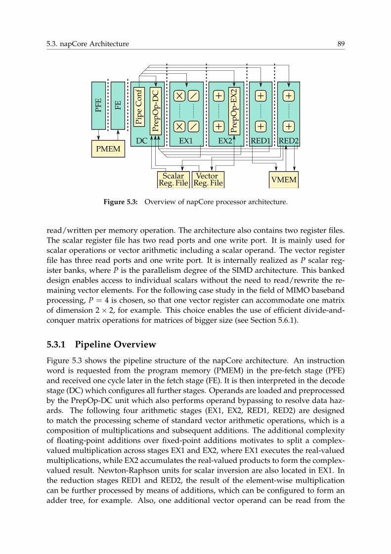
5.3. napCore Architecture 89
PFE
FE
DC
Prep
Op-
DC
Scalar
EX1 EX2 RED1
Prep
Op-
EX2
RED2Pi
peC
onf
PMEM
VMEMVectorReg. File Reg. File
Figure 5.3: Overview of napCore processor architecture.
read/written per memory operation. The architecture also contains two register files.The scalar register file has two read ports and one write port. It is mainly used forscalar operations or vector arithmetic including a scalar operand. The vector registerfile has three read ports and one write port. It is internally realized as P scalar reg-ister banks, where P is the parallelism degree of the SIMD architecture. This bankeddesign enables access to individual scalars without the need to read/rewrite the re-maining vector elements. For the following case study in the field of MIMO basebandprocessing, P = 4 is chosen, so that one vector register can accommodate one matrixof dimension 2× 2, for example. This choice enables the use of efficient divide-and-conquer matrix operations for matrices of bigger size (see Section 5.6.1).
5.3.1 Pipeline Overview
Figure 5.3 shows the pipeline structure of the napCore architecture. An instructionword is requested from the program memory (PMEM) in the pre-fetch stage (PFE)and received one cycle later in the fetch stage (FE). It is then interpreted in the decodestage (DC) which configures all further stages. Operands are loaded and preprocessedby the PrepOp-DC unit which also performs operand bypassing to resolve data haz-ards. The following four arithmetic stages (EX1, EX2, RED1, RED2) are designedto match the processing scheme of standard vector arithmetic operations, which is acomposition of multiplications and subsequent additions. The additional complexityof floating-point additions over fixed-point additions motivates to split a complex-valued multiplication across stages EX1 and EX2, where EX1 executes the real-valuedmultiplications, while EX2 accumulates the real-valued products to form the complex-valued result. Newton-Raphson units for scalar inversion are also located in EX1. Inthe reduction stages RED1 and RED2, the result of the element-wise multiplicationcan be further processed by means of additions, which can be configured to form anadder tree, for example. Also, one additional vector operand can be read from the

90 Chapter 5. napCore: An ASIP for MIMO Baseband Processing
vBP
vREG
sBP
sREG
is_bp
is_bp
4
4
1
1
4
1
&
1
1
1
s1 s4
DC
Pipe
line
reg.
DC
-EX
1
EX1
vreg_idxelem_idx
sreg_idx
1
1
1
1
cfg_pis2 s3
&
&
&
π
Figure 5.4: Schematic of data acquisition for first operand.
vector register file by the PrepOp-EX2 unit in EX2 to serve as input to RED1 (e.g.,for multiply-accumulate operations). Results are written back to the vector memory(VMEM) or the scalar/vector register files after processing is completed in the RED2stage.
5.3.2 Operand Acquisition
For programmable architectures with inherent parallelism like SIMD or VLIW proces-sors, the potential for data-level parallelism is defined by the parallelism of the datapath, given there is an efficient operand acquisition mechanism. Even for regular vec-tor arithmetic operations, this is a challenging task. Depending on the instruction,very different data access patterns have to be realized for the previously describedSIMD architecture with a scalar and a vector register file, for example. This, in turn,leads to the complex operand acquisition circuitry depicted in Figure 5.4 for the firstoperand. Widths of the data path are given as multiples of complex-valued scalars.
The vector and scalar register files vREG and sREG are accessed depending on thetype of the operand. Bypassing units vBP and sBP attempt to obtain the demandedoperand from the pipeline, where it is potentially present as the result from a previousoperation (see Section 5.3.3) and signal the successful acquisition (is_bp) to the subse-quent multiplexer. In the next step, the required scalar elements are sent to the fourmantissa masking units marked by &. The switch s3 configures if the operand to loadis scalar or vectorial and accordingly activates the first or all masking units. A scalaroperand, however, can come from a scalar register or one element of a vector registeras configured by s2. If the scalar comes from the vector register, the right element isselected by s1. The masked operands are forwarded to the pipeline register betweenstages DC and EX1. In case the same scalar element is to be forwarded to all elementsof the operand, as required for a scalar-vector multiplication for example, this can betriggered by s4. Otherwise the masking results are forwarded element by element.When fetching the operand in the EX1 stage, there is an additional permutation unitmarked as π.

5.3. napCore Architecture 91
hilo1 hilo2
cb1
hilo3
cb2 cb3
Op.
1
Op.
2
hilo4
Figure 5.5: Permutation units for vector operands.
Figure 5.5 shows a schematic overview of the permutation networks for the twovector operands in front of the multipliers in EX1. Apart from straight pass-through,the networks support patterns tailored to 2× 2 vector arithmetic operations like ma-trix inversion, determinant calculation, or matrix-matrix multiplication. Since the firstvector operand (Op. 1) typically holds the left-hand value of a multiplication and 2× 2matrices are stored row-wise in the vector registers, the left and right pair of multi-plexers are wired to select one of the two matrix rows via hilo1 and hilo2. Furthermore,the crossbar cb1 allows to repeat the same scalar element twice at the output. The pathfor the second vector operand (Op. 2) contains the same set of multiplexers. Since theright-hand value of a matrix multiplication is typically accessed column-wise whilethe matrix is stored row-wise, the input can be transposed via crossbar cb2. Cross-bar cb3 is used to realize further permutations (e.g., for 2× 2 matrix inversion). Thisflexible operand acquisition paired with the P-wise partitioned vector register file al-lows versatile data access schemes like obtaining scalars from the scalar register fileor from elements of the vector register file, the use of vector elements in scalar opera-tions, and using scalar elements (from vREG as well as sREG) in vectorial operations.Still, it should be noted that such permutation units are not required at all for parallelSIMD architectures.
5.3.3 Operand Bypassing
The bypassing units vBP and sBP in the DC stage attempt to fetch an operand fromthe pipeline as a result of a previous instruction instead of waiting until it becomesavailable in the register file after passing through the pipeline. Since the ALU ofthe napCore architecture spans across several pipeline stages, the bypassing unitshave to know for each instruction at which stage of the pipeline its computation isfinished. When executing a component-wise complex multiplication of two vectorsfor example, the result is valid after the summation of the partial products in the EX2stage and can be bypassed from there. To inform vBP and sBP about this context,the decoding circuit injects an index into the pipeline for each decoded instruction,indicating after how many arithmetic stages its result is valid. The bypassing logicuses this information to decide whether or not an operand is bypassed. Since anadditional vector operand can be loaded as input to the RED1 stage, one further

92 Chapter 5. napCore: An ASIP for MIMO Baseband Processing
s e e e e e m m m m m m m m m
&
man
-msk
Figure 5.6: Mantissa masking.
operand preprocessing unit (PrepOp-EX2) is located in the EX2 stage. The majordifference between PrepOp-DC and PrepOp-EX2 is that there is no bypassing in thelatter, and it obtains just one vector from the vector register file.
5.3.4 Numerically Aware Processing
Many algorithms can be decomposed into distinct sections of different requirementsfor numerical precision, as will be demonstrated in Section 5.6.1 for the exemplarycase of two equalizer-based MIMO detection algorithms. For a floating-point number(see (5.1)), the normalized nature of the floating-point mantissa, which guarantees1 ≤ m < 2, can be exploited. Normalization assures that masking a certain numberof least significant bits (LSBs) of the mantissa, in the following referred to as mantissamasking, will always leave the same number of most significant bits (MSBs). Note thatthis is not the case for fixed-point data formats, where the MSB may be located atany bit position within a data word. Accordingly, mantissa masking is more suitablefor floating-point number formats. The principle is illustrated in Figure 5.6, wherea variable bitmask is applied to the last four LSBs of an exemplary floating-pointnumber format. The width of the bitmask has to be chosen according to the variationof precision requirements in the target application domain. For the napCore, onemasking unit is placed as in Figure 5.6 at the end of operand loading in PrepOp-DCas well as after every arithmetic component within the 4-stage ALU. The bitmask canbe adapted at runtime by a configuration instruction in the program code.
5.3.5 Floating-Point Newton-Raphson Iterator
One common task in vector arithmetic is vector norming, which requires the calcu-lation of a scalar reciprocal. This operation is one of the few examples where thefloating-point arithmetic unit is less complex than its fixed-point counterpart, as willbe illustrated in the following. Since root finding problems like scalar reciprocals arecomputationally complex, they are typically approximated by the Newton-Raphsonalgorithm [92] which finds the nulls of a function f by iteratively calculating
yn+1 = yn −f (yn)
f ′(yn)n = 0, 1, 2, .. (5.2)

5.3. napCore Architecture 93
res0
res1
res2
res3
vr0
vr1
vr2
vr3 Pipe
line
regi
ster
RED
1-R
ED2
0
Pipe
line
regi
ster
EX2-
RED
1
RED2RED1
no_red1 fw cfg_pi no_red2 no_red3 no_red4
π
Figure 5.7: Configurable reduction stages RED1 and RED2.
given an initial choice of y0, where f ′ is the derivative of function f . To find y = 1/x,the nulls of the function f (y) = 1/y − x have to be determined. In that case, theiteration according to (5.2) is given by
yn+1 = 2yn − y2nx, (5.3)
where the napCore calculates one iteration per cycle. The choice of a suitable initialy0 close to the converging point of the iteration is essential for fast convergence. Fora floating-point number as in (5.1), the scalar reciprocal is calculated as
1a= sgn · 1
m· 2−e. (5.4)
Since mantissa m lies in the range of 1 ≤ m < 2, the reciprocal mantissa is alsolimited in range (0.5 < 1/m ≤ 1). Thus, the selection of y0 is less complex thanfor a fixed-point implementation, where the range of the input operand has to beconsidered explicitly. This allows the implementation of a simple two-choice selectionmechanism, dividing the solution space into two parts of equal size. Four subsequentNewton-Raphson iterations are sufficient for the baseband applications described inSections 2.4.2.1 and 2.4.2.2.
5.3.6 Configurable Reduction Stages
To support a versatile instruction set (e.g., for efficient processing of vectorial dataof different dimensions), the reduction stages RED1 and RED2 are designed to fitthe requirements of a wide range of vector arithmetic operations. The maximumnumber of required complex adders in RED1 corresponds to SIMD parallelism degreeP, which is needed if a multiply-accumulate operation with P-dimensional vectoroperands is executed. Note that for an inner product, an adder tree of depth ld(P)

94 Chapter 5. napCore: An ASIP for MIMO Baseband Processing
is sufficient, which requires P/2 adders in RED1 (if P is a power of 2). In RED2,P/4 adders are sufficient for an inner product, but for the configuration of P = 4,an additional adder is placed in RED2, where it is used for specialized instructionsfor√
P×√
P vector arithmetic (the dimension for which one square matrix fits intoone vector register). Figure 5.7 shows parts of the reduction stages RED1 and RED2for P = 4. For reasons of simplicity, not all multiplexing and demultiplexing controlsignals are included. As previously discussed, there are four and two complex addersin RED1 and RED2, respectively. To support various vector arithmetic operations,the additions in stages RED1 and RED2 require flexible interconnects. The inputto RED1 can come from the result of previous pipeline stages (res0. . . res3) or fromthe vector register file (vr0. . . vr3), whose content can also be forwarded to RED2(fw). If no additions are required for the current instruction, the result from EX2can also be simply forwarded through the pipeline by setting no_red1. . . no_red4. Aswill be shown in Section 5.6.1, support for
√P×√
P vector arithmetic enables efficientdivide and conquer algorithms (e.g., for matrix inversion). The price to pay to supportthese operations is the permutation network marked as π in front of the adders inFigure 5.7, configurable via cfg_pi. Once again, the multiplexing, demultiplexing, andpermutation logic depicted in Figure 5.7 would not be necessary for a purely parallelSIMD architecture like the Huawei baseband DSP that is described in the next sectionfor comparison.
5.4 Huawei Baseband DSP Architecture
The Huawei baseband DSP discussed in the scope of this work is a research pro-cessor core designed for baseband processing in LTE [38] base stations. The core isC-programmable and special features (e.g., SIMD support) are accessible as C intrin-sics. Starting point of the design is a Cadence® Tensilica® Xtensa® basic 32-bit RISCcore [22] that is extended by further functionality for baseband processing. The corehas SIMD capabilities, but these are not motivated by the high share of vector arith-metic in MIMO baseband processing but by the high degree of data-level parallelismin multicarrier transmission schemes like LTE [38]. For that reason, the vector datapath of the Huawei baseband DSP is designed for parallel SIMD execution. The pro-cessor has a VLIW instruction set architecture, where the vector data path is controlledby one instruction slot. Figure 5.8 gives an overview of the instruction set architecture.One VLIW instruction word has four instruction slots (slot 0 to 3) that are describedin the following.
Slot 0 contains all Xtensa base functionality as well as load/store operations fromthe memory to the vector registers or vice versa. Slot 1 controls the floating-pointvector data path with support for complex-valued as well as real-valued multiply-accumulate operations with a SIMD parallelism degree of four. Within this work,the design-time configurable wordwidth of floating-point data in the vector data pathis set to 20 bit. The 20-bit floating-point words are extended back to 32-bit singleprecision floating-point when written back to the memory. In addition to the standard

5.5. Synthesis Results 95
CTRL + vector L/S Vector data path CTRL + Misc. DFT- All Xtensa base- Queue port- Vector load/store- All single VR move- 16/32 bit imm.
- FP vector MAC- FP vector conditional
- Some Xtensa base- Vector load- Vector select ops- Vector table ops- Vector move ops- FP scalar ALU- 16/32 bit imm.
- Exponential
Slot 0 Slot 1 Slot 2 Slot 3
Figure 5.8: Overview of Huawei baseband DSP instruction set architecture.
32-bit scalar register file, there is a vector register file with storage for 24 vector words.Slot 2 contains some Xtensa base functionality as well as support for vector dataloading/movement. Slot 3 is dedicated to computations on the exponent of complex-valued numbers. This is used for DFT/iDFT calculations, for example. Similar tothe napCore architecture, the Huawei baseband DSP implements NAP for its vectordata path by masking a configurable number of LSBs of the floating-point mantissaat the inputs of all arithmetic functional units in the vector data path. In this context,functional units are defined on the granularity of elementary arithmetic operationslike real-valued additions or multiplications. This means that in the vector data path,there is one masking unit in front of the real-valued multiplication in each complex-valued multiply-accumulate unit. The next mask is in front of the addition of thepartial products to form results of complex-valued multiplications, and the final one isin front of the adders for the accumulation part of the multiply-accumulate operation.
The memory subsystem of the Huawei baseband DSP is a Harvard architecturewith distinct data and program memories. The program memory subsystem containstwo memory blocks with 1024 words each. The data memory is composed of fivememory blocks, each with storage for 512 vector words.
5.5 Synthesis Results
This section discusses synthesis results of the napCore architecture and identifies de-sign points optimizing throughput, area efficiency, and energy efficiency, respectively.Based on this analysis, the potential for energy savings using mantissa masking isevaluated. Finally, napCore synthesis results are compared with the Huawei base-band DSP introduced in Section 5.4.
5.5.1 Design Space Exploration
Figure 5.9a presents synthesis results of the napCore architecture for different floating-point number formats. Here, s stands for the sign bit, m represents the number ofmantissa bits, not including the redundant leading MSB (hidden bit), and e stands

96 Chapter 5. napCore: An ASIP for MIMO Baseband Processing
1.8 2 2.2 2.4 2.6 2.880
100
120
140
160
180
200
220
Tclk [ns]
Har
dwar
eco
mpl
exit
y[k
GE]
s1m8e6s1m12e6s1m16e6
(a) Hardware efficiency.
1.8 2 2.2 2.4 2.6 2.80.2
0.4
0.6
0.8
1
1.2
Tclk [ns]En
ergy
per
cycl
e[n
J]
s1m8e6s1m12e6s1m16e6
(b) Energy efficiency.
Figure 5.9: napCore synthesis results (90 nm CMOS, 1 V supply voltage).
for the number of exponent bits. The design is synthesized for a 90 nm standard per-formance CMOS technology under typical conditions with a supply voltage of 1 V.On the Y-axis, the figure shows the hardware complexity AGE as number of requiredkilo gate equivalents (kGE) without memory as a function of the clock period Tclk onthe X-axis. The figure allows the identification of the design points with maximumarchitectural throughput as well as the minimum area-timing (AT) products, whichrepresent the design points for maximum hardware efficiency.
Figure 5.9b shows the results of an energy benchmark for the same clock frequen-cies and number formats as presented in Figure 5.9a. The Y-axis shows the averageenergy consumption E per clock cycle. Results are derived based on averaged poweranalysis of topographical gate-level models of the processor architecture. The bench-mark program consists of a series of matrix-vector multiplications implemented byinner products, thus, it occupies all ALU stages of the pipeline simultaneously andis a good indicator for the energy consumption under full load. Naturally, a relaxedtiming constraint during synthesis allows for a more energy-efficient hardware im-plementation, but the decrease of E(Tclk) shows saturating behavior, so at a certainpoint, the marginal decrease in energy consumption does not justify lowering theclock frequency. As a result, this plot allows the identification of the design pointsfor energy efficiency in the saturation area of E(Tclk). The results from Figure 5.9aand Figure 5.9b are summarized in Table 5.1, giving the clock frequency at the designpoints for maximum throughput f T
clk, maximum hardware efficiency f Aclk, and energy
efficiency f Eclk as well as the corresponding hardware complexities AT
GE, AAGE and AE
GE.Table 5.2 gives a more detailed overview of the power breakdown of the napCore
architecture for number formats s1m8e6, s1m12e6 and s1m16e6. Here, as well as for the

5.5. Synthesis Results 97
s1m8e6 s1m12e6 s1m16e6
f Tclk 588 526 476
f Aclk 500 476 435
f Eclk 435 400 385
ATGE 131 160 198
AAGE 96.1 137 176
AEGE 88.1 123 162
Table 5.1: Clock frequency fclk [MHz] and hardware complexity AGE [kGE] for dif-ferent design points of napCore architecture.
s1m8e6 s1m12e6 s1m16e6
mW % mW % mW %
EX1 44.4 33.9 90.4 45.2 148.0 51.2EX2 15.8 12.1 20.3 10.1 27.4 9.5RED1 9.6 7.3 13.2 6.6 18.4 6.4RED2 11.2 8.5 14.9 7.4 20.0 6.9PMEM 9.6 7.3 8.9 4.5 8.6 2.9REG 11.5 8.8 13.5 6.8 17.3 6.0MISC 28.9 22.1 38.8 19.4 49.3 17.1
Σ 131 200 289
Table 5.2: Post-synthesis power breakdown of napCore architecture under full loadbenchmark.
remainder of this chapter, all configurations are synthesized at the design point forenergy efficiency. The table shows the power consumption of the arithmetic stages,the program memory and the register files as well as further miscellaneous parts likecontrol and pipeline registers. For all configurations, the major share of the poweris consumed by the 16 multipliers in the EX1 stage, and their share increases whenraising the number of mantissa bits from eight (33.9 %) to 16 (51.2 %). The secondlargest share comes from the floating-point adders in the remaining ALU stages. Afraction of around 62 to 74 % of the total energy is consumed within the ALU. Theremainder is distributed among control, memory accesses, register file accesses, andswitching activity within pipeline registers.

98 Chapter 5. napCore: An ASIP for MIMO Baseband Processing
4 6 8 10 12 14 160.1
0.2
0.3
0.4
0.5
0.6
0.7
0.8
Mantissa bits
Ener
gype
rcy
cle
[nJ]
s1m8e6 EPclk
s1m8e6 EALUclk
s1m12e6 EPclk
s1m12e6 EALUclk
s1m16e6 EPclk
s1m16e6 EALUclk
Figure 5.10: Post-synthesis energy consumption per cycle under full load bench-mark for s1m8e6, s1m12e6 and s1m16e6.
5.5.2 Energy Benchmark for Mantissa Masking
To assess the potential energy savings achievable by adaptive mantissa precision, thesame benchmark as presented in Section 5.5.1 is executed for core configurationss1m8e6, s1m12e6 and s1m16e6. The mantissa width is reduced bit by bit in softwareat runtime so the changes in energy consumption can be observed. The results areshown in Figure 5.10. The first triplet of lines (suffix EP
clk) shows the energy consump-tion of the entire processor core, while the second triplet (suffix EALU
clk ) solely containsthe energy consumed within the arithmetic logic stages EX1, EX2, RED1 and RED2.
Figure 5.10 outlines the potential as well as limitations of mantissa masking. Onthe one hand, it demonstrates that the runtime-adaptive mantissa format enables en-ergy savings which show nearly linear behavior with respect to the chosen word-width. On the other hand, there is still an overhead of masking down the mantissaformat as opposed to using arithmetic units which natively support the required pre-cision. This overhead shows in the difference in energy consumption per cycle be-tween core configurations s1m16e6 and s1m12e6 for 12 mantissa bits, for example. Fors1m16e6, mantissa masking decreases energy consumption from 0.780 nJ using fullprecision to 0.669 nJ by masking four mantissa LSBs. However, in native s1m12e6arithmetic, the operation only consumes 0.539 nJ.
5.5.3 Comparison with Huawei Baseband DSP
For this work, the Huawei baseband DSP was synthesized for a 28 nm CMOS technol-ogy with a clock frequency of 800 MHz. Scaled to 90 nm CMOS, this corresponds to aclock speed of 248 MHz. The vector data path operates on 20-bit floating-point valueswith a s1m12e7 configuration. Synthesis results are summarized in Table 5.3.
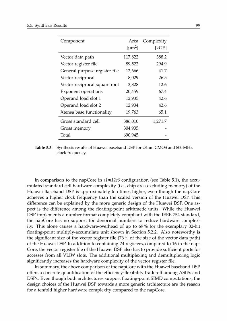
5.5. Synthesis Results 99
Component Area Complexity[µm2] [kGE]
Vector data path 117,822 388.2Vector register file 89,522 294.9General purpose register file 12,666 41.7Vector reciprocal 8,029 26.5Vector reciprocal square root 3,828 12.6Exponent operations 20,459 67.4Operand load slot 1 12,935 42.6Operand load slot 2 12,934 42.6Xtensa base functionality 19,763 65.1
Gross standard cell 386,010 1,271.7Gross memory 304,935 -Total 690,945 -
Table 5.3: Synthesis results of Huawei baseband DSP for 28 nm CMOS and 800 MHzclock frequency.
In comparison to the napCore in s1m12e6 configuration (see Table 5.1), the accu-mulated standard cell hardware complexity (i.e., chip area excluding memory) of theHuawei Baseband DSP is approximately ten times higher, even though the napCoreachieves a higher clock frequency than the scaled version of the Huawei DSP. Thisdifference can be explained by the more generic design of the Huawei DSP. One as-pect is the difference among the floating-point arithmetic units. While the HuaweiDSP implements a number format completely compliant with the IEEE 754 standard,the napCore has no support for denormal numbers to reduce hardware complex-ity. This alone causes a hardware-overhead of up to 69 % for the exemplary 32-bitfloating-point multiply-accumulate unit shown in Section 5.2.2. Also noteworthy isthe significant size of the vector register file (76 % of the size of the vector data path)of the Huawei DSP. In addition to containing 24 registers, compared to 16 in the nap-Core, the vector register file of the Huawei DSP also has to provide sufficient ports foraccesses from all VLIW slots. The additional multiplexing and demultiplexing logicsignificantly increases the hardware complexity of the vector register file.
In summary, the above comparison of the napCore with the Huawei baseband DSPoffers a concrete quantification of the efficiency-flexibility trade-off among ASIPs andDSPs. Even though both architectures support floating-point SIMD computations, thedesign choices of the Huawei DSP towards a more generic architecture are the reasonfor a tenfold higher hardware complexity compared to the napCore.

100 Chapter 5. napCore: An ASIP for MIMO Baseband Processing
5.6 Case Study: Equalizer-Based MIMO Detection
In the following case study, the concept of NAP is applied to equalizer-based MIMOdetection. The open-loop and iterative equalizer-based detection algorithms that areemployed in this chapter were previously introduced in Section 2.4.2.1 and 2.4.2.2, re-spectively. Their software implementation on the napCore is discussed in Section 5.6.1,including an evaluation of the required numerical precision. After that, a layoutedversion of the processor core for the maximum required precision is presented inSection 5.6.2 and used in Section 5.6.3 to evaluate the efficiency of the implementa-tions of the previously introduced algorithms. Based on these efficiency benchmarks,Section 5.6.4 compares the napCore to other architectures from the literature.
5.6.1 Software Implementation
For open-loop detection, equalization and SINR calculation are subdivided into threeclasses of different numerical precision requirements. The first one, Pmul
ol , is used inthe multiplicative part of equalization (see (2.32)), namely calculating
Aol =(
HHH + N0IMS
)and subsequently
s = A−1ol HHy. (5.5)
The class P invol covers the inversion of A−1
ol itself, while P llrol includes deriving the SINR
as in (2.34), which is later used for LLR calculation. The precision requirements ofthese classes are presented at the end of this section. Similar to open-loop detection,three different classes of precision requirements are defined for iterative detection.The class Pmul
it covers the calculation of
Ait =(
HHHΛz + N0IMS
)(5.6)
as well as the interference mitigated vectors yi in (2.36). The class P invit contains the
actual matrix inversion of A−1it , and P llr
it is used for the calculation of SINRs, whichare used later for LLR computation. The aforementioned precision classes are chosenso that the implementation of the algorithms on the napCore achieves the same com-munication performance as the reference floating-point implementation. The achiev-able FER for the maximum 4× 4 antenna constellation is shown in Figure 5.11 for4-QAM, 16-QAM, and 64-QAM for open-loop detection and iterative detection withone detector-decoder iteration. The data payload of one frame in terms of informationbits corresponds to the size of one MSDU in the IEEE 802.11 [71] standard. FERs arederived from extensive Monte Carlo simulations for a 4× 4 MIMO setup with an i.i.d.Rayleigh slow fading channel superimposed by AWGN. The power delay profile ofthe channel impulse response is modeled according to the TGn-C model [36]. The
2 it-0 and it-1 denote initial open-loop detection and first iterative detection

5.6. Case Study: Equalizer-Based MIMO Detection 101
6 8 10 12 14 16 18 20 22 24 26 28 30 3210−3
10−2
10−1
100
SNR
FER
4-QAM it-0 16-QAM it-0 64-QAM it-04-QAM it-1 16-QAM it-1 64-QAM it-1
Figure 5.11: FER for open-loop and iterative 4× 4 MIMO detection using 4-QAM,16-QAM, and 64-QAM constellations. OFDM tones: 64. OFDM datatones: 52. Frame size: 2,304 byte (uncoded). Channel coding: convolu-tional (g0 = 133o , g1 = 177o), code rate: 1/2. Channel decoding: BCJR.Channel model: slow fading.
receiver setup is chosen as depicted in Figure 4.1 with convolutional channel codingof rate R = 1/2, using generator polynomials g0 = (133)8 and g1 = (171)8. Channeldecoding is performed according to the BCJR algorithm [85].
For a software implementation, the previously introduced algorithms have to bemapped onto the proposed processor architecture. The algorithmic design space,particularly for the inversion of Aol and Ait, was explored in Section 4.3. Now, asuitable candidate has to be picked for the napCore architecture. A vectorial SIMDcore is inherently suitable for vector arithmetic like the calculation of Aol in (5.5)and Ait in (5.6). As discussed in Section 5.3.6, the napCore supports 2 × 2 matrixoperations, where each matrix is stored in a single vector register. These operationsenable an efficient implementation of higher order matrix inversions using a DnQalgorithm based on the Schur complement [1]. The computational complexity of theDnQ algorithm was compared to other algorithms in Section 4.3 and found to beslightly more complex than the LU-based variant. However, its regular data accesseson same-size data fragments make it a better fit for the napCore architecture. TheLTE [38] uplink equalizer-based MIMO detector implemented on the Huawei DSP isformulated slightly different from the algorithms in Section 2.4.2.1 and 2.4.2.2, sincethe uplink scenario also has to compensate interference from other users. Anotherdifference is that the equalizer matrices for the LTE [38] implementation are hermitianfor both the open-loop and the iterative case [50]. Since the generic nature of the DSPdoes not impose a bias towards any inversion algorithm, LDLh is selected because ithas the lowest computational complexity of the researched algorithms.

102 Chapter 5. napCore: An ASIP for MIMO Baseband Processing
Antenna setup 2 x 2 2 x 4 4 x 4 4 x 8
Open-loop 22 24.5 80 101Iterative 32.5 35 112 137
Table 5.4: Cycle count of equalizer-based MIMO detection on napCore architecture.
On the napCore, MIMO detection for multiple antenna setups (e.g., 2× 2, 2× 4,4 × 4 and 4 × 8) can be efficiently implemented based on (4.41) and (4.43). Cyclecounts for the execution of MIMO detection including equalizing and SINR calcu-lation are listed in Table 5.4 for the aforementioned setups3. In Section 4.4.3, thenumber of STxP70 and C64x+ cores required for real-time capable open-loop detec-tion was calculated as a function of the frame size for the 20 MHz mode of the IEEE802.11 standard [71]. The dependency on the frame size occurs for these two processorcores because the upfront matrix inversion necessary for equalizer matrix calculationrequires more execution time than the duration of the block preamble. This causes abacklog that has to be compensated during the multiplication of equalizer matricesand receive symbol vectors. For the napCore, on the other hand, even the 4× 4 matrixinversion requires only 47 cycles. This is sufficiently short to not cause any backlogeven for a single napCore instance according to the layout from Section 5.6.2, whichruns at 400 MHz for 90 nm CMOS. As a result, the number of cores required for real-time operation does not depend on the frame length. For open-loop detection, twocores suffice according to (4.67). Since iterative detection equalizer matrices have tobe recalculated for each receive symbol vector, the computational load is significantlyhigher, and real-time iterative detection, including the initial open-loop detection, re-quires five cores. When scaled to 28 nm CMOS for comparability with the STxP70core, these numbers reduce to one and two respectively.
In the following, the numerical precision requirements of the previously intro-duced six precision classes are analyzed, when using the DnQ matrix inversion algo-rithm. For this analysis, the number format of each precision class is reduced untilit causes a perceivable impact on the FER shown in Figure 5.11. Table 5.5 shows therequired mantissa bits for all precision classes. One sees an increase in precision re-quirements for more dense constellations due to the narrower margin of error. Thematrix inversion generally turns out to have a higher precision requirement than themultiplicative section because of the higher dynamic range, which can be mainly lo-cated within the determinant calculation. Only the SINR calculation has a constantprecision requirement, since the channel decoder’s algorithmic performance dependson the LLR precision and not on the used constellation. Also, it is interesting toobserve the drop in precision requirements from the initial open-loop detection tothe subsequent iterative detection. These findings can be exploited by the flexiblecharacteristics of the napCore to reduce energy consumption.
3 Half cycles in Table 5.4 are due to the interleaved processing of two subcarriers.

5.6. Case Study: Equalizer-Based MIMO Detection 103
P invol Pmul
ol P llrol P inv
it Pmulit P llr
it
4-QAM m8 m7 m4 m5 m4 m416-QAM m11 m10 m4 m8 m7 m464-QAM m12 m11 m4 m11 m10 m4
Table 5.5: Precision requirements for open-loop and iterative 4× 4 MIMO detection.
Register File
EX1
RED2
RED1_RED2
PFEFE
PMEMVMEM1
VMEM2
EX2
DCRED1
EX2_RED1
DC_EX1
EX1_EX2
napCore
Figure 5.12: Layout of napCore with s1m12e6 configuration for energy efficiency us-ing 90 nm CMOS technology and 1 V supply voltage.
5.6.2 Layout Implementation
Table 5.5 identifies the s1m12e6 floating-point number format as the maximum preci-sion requirement for the previously introduced equalizer-based detection algorithms.To prove the feasibility of the napCore architecture, this section presents a post-layoutmodel for that particular precision at the design point for energy efficiency. For in-creased accuracy, all following assessments of energy efficiency are based on thatmodel. Figure 5.12 shows the physical view of the architecture implementation, over-laid with the interpolated borders between the pipeline stages, pipeline registers (e.g.,DC_EX1 marks the pipeline register between the DC stage and the EX1 stage) as wellas program and vector memory. The layout achieves the target frequency of 400 MHz.One clearly sees the high wiring effort on the top metal layer (in turquoise) to connectthe vector register file to the DC stage, as well as the strategic placement of the DCstage itself in the middle of the design to facilitate vector bypassing from all compu-tational stages back to DC. Another contribution to the dense wiring in the DC stage

104 Chapter 5. napCore: An ASIP for MIMO Baseband Processing
4-QAM 16-QAM 64-QAM full prec.
mW nJ mW nJ mW nJ mW nJ
it-0 119 23.8 134 26.8 138 27.6 143 28.6it-1 86.9 24.3 105 29.4 117 32.8 124 34.7
Table 5.6: Power and energy consumption of equalizer-based 4× 4 MIMO detectionon s1m12e6 napCore.
results from the flexible operand acquisition logic described in Section 5.3.2. Also theregister file is strategically located close to the DC stage for operand loading as wellas to the RED2 stage for operand writeback.
The design presented in Figure 5.12 contains a vector memory for 512 vectorwords of length 152 bit, which is partitioned into two memory banks. The instruc-tions are fetched from a dedicated program memory with space for 1024 words of32 bit. For the sake of flexibility and extendability, the program memory size issignificantly higher than the number of instructions required for MIMO detection.Similarly, the aforementioned detection implementations operate on the register filesexclusively and the vector memory is only included to support further potential ap-plications with higher caching needs. The total design dimension (including memoryand power rings) is 965 µm by 1020 µm resulting in a total area of 0.984 mm2. Theupper part containing the pipeline and the register file measures 597 µm by 905 µmtotaling an area of 0.540 mm2. Based on the post-layout model, energy consumptionwas re-evaluated and found to be around 30 to 40 % higher than for the topographicalgate-level model, depending on the application.
5.6.3 Use Case Energy Assessment
In the following, the energy efficiency of open-loop and iterative equalizer-basedMIMO detection is assessed. The results of this analysis are shown in Table 5.6 forprecisions as in Table 5.5 and full precision as reference. Energy and power valuesare given per iteration (i.e., not including previous iterations). As predicted, energyconsumption drops when switching to lower order constellations with lower preci-sion requirements. When comparing the open-loop variant with iterative detection,the power consumption of the former is notably higher. This can be explained by thehigher precision requirements in it-0 and by the fact that the values themselves startconverging in it-1, which reduces switching activity. Due to the shorter executiontime, the energy consumption of open-loop detection is still less than for the iterativevariant, though.
It shall be noted here that there is not just one correct precision and thus oneenergy number per use case. The precisions shown in Table 5.5 are only necessary toachieve the same communication performance as the double precision floating-point

5.6. Case Study: Equalizer-Based MIMO Detection 105
Target FER P inv Pmul P llr E [nJ]
Open-loop detection at 24 dB
T1 m8 m7 m3 23.8T2 m9 m8 m3 24.8T3 m11 m10 m4 26.8
Iterative detection at 19 dB
T1 m4 m3 m2 24.1T2 m5 m4 m3 24.5T3 m8 m7 m4 29.4
Table 5.7: Communication performance vs. energy, 4 × 4 MIMO detection (16-QAM).
reference implementation. Depending on the application, this kind of communica-tion performance may not be required, for example if a lower data rate would alsosuffice for the application to function correctly or when a few compromised bits donot diminish the overall user experience. As a result, it makes sense to trade energysavings for communication performance (e.g., in terms of FER), depending on the ap-plication requirements. Table 5.7 illustrates this trade-off for open-loop and iterativedetection using a 16-QAM constellation. It shows the reduction of numerical preci-sion requirements for FER targets T1, T2 and T3 in the range of 1 · 10−1, 5 · 10−2 and1 · 10−2 at reference SNRs of 24 dB for open-loop and 19 dB for iterative detection.The complete FER trajectory for iterative detection subject to this precision reductionis shown in Figure 5.134. It is interesting to see that already for target T2, the mantissawidth can be reduced from eight to five or less bits for iterative detection. This factmight potentially be exploited by integrating a set of small integer multipliers into thefloating-point data path to handle operations with less precision requirements. Thegain of such a measure can be approximated based on Figure 5.10. Figure 5.13 alsoshows the achieved data rate which is the amount of correctly transfered informationbits per unit of time. The data rate depends on the FER and the use case (i.e., antennasetup, code rate, constellation alphabet, etc.) and is discussed in more detail in Sec-tion 7.1. Already at an SNR of 18 dB, the reduced precision class T2 delivers 97 % ofthe data rate of the double-precision floating-point equivalent class T3.
5.6.4 Comparison with State-of-the-Art
To assess the efficiency of the napCore design, a literature based comparison withstate-of-the-art equalizer-based MMSE MIMO detectors for a 4 × 4 antenna config-uration is conducted. The results of this comparison are summarized in Table 5.8.
4 The unsteady trajectories of the curves for targets T1 and T2 are caused by numerical effects, not byshort simulation time.

106 Chapter 5. napCore: An ASIP for MIMO Baseband Processing
10 12 14 16 18 20 2210−3
10−2
10−1
100
SNR
FER
10 12 14 16 18 20 220
20
40
60
80
100
SNRD
ata
rate
[Mbi
t/s]
T1T2T3
Figure 5.13: FER and data rate degradation caused by reduced numerical precisionfor 4× 4 iterative MIMO detection (it-1) using a 16-QAM constellation.OFDM tones: 64. OFDM data tones: 52. Frame size: 2,304 byte (un-coded). Channel coding: convolutional (g0 = 133o , g1 = 177o), coderate: 1/2. Channel decoding: BCJR. Channel model: slow fading.
The implementation levels range from synthesized via layouted down to silicon im-plementations. Since equalizer-based detectors operate on symbol vectors, hardwareand energy efficiency are defined as processed symbol vectors per second and gateequivalent (vec/s/GE) and processed symbol vectors per unit of energy (vec/nJ), re-spectively. For comparability with [103], energy consumption is listed for the useof a 64-QAM constellation. It is not straightforward how to include the silicon areaof the memories within the napCore into the comparison, since neither of the twoequalizer-based detection algorithms requires caching in the vector memory. Also theapplication size of the equalizer-based MIMO detection algorithms is around 10 % ofthe available program memory, which can be considered negligible compared to therest of the design. Therefore, memory is not included in the area comparison. Energyefficiency is given including memories, though.
When assessing programmability and flexibility, different architectures can becharacterized by their programming interface and data path reconfigurability. Thetailored ASIC designs [20] and [103] both have no programming interface and are in-ternally controlled by an FSM. The adaptive stream processing engine (ASPE) [33] isprogrammed in a VLIW-like fashion to configure the data flow through the functionalunits before stream processing begins. Even though an up-front configured data pathsupersedes accesses to the program memory during execution, it limits potential ap-plications to those with a repetitive, regular data flow. Also, high throughput can onlybe guaranteed if a sufficient number of functional units is available to occupy the com-plete width of the processing pipeline. Therefore, the architecture can be considered

5.6. Case Study: Equalizer-Based MIMO Detection 107
moderately flexible. The remaining architectures sequentially reconfigure their datapath for each instruction. In [34], an assembly-programmable array of floating-pointmultiply-accumulate elements is shown, but the authors explicitly mention the limitedflexibility of the data path. The reconfigurable ASIP (rASIP) design in [26] containsa two-dimensional coarse grained reconfigurable array (CGRA) configured by a RISCcore via a configuration memory. While the RISC core can be easily programmed inassembly, the functional units of the CGRA have to be programmed by a configurationbitstream, which limits the ease of programming. Also, the structure of the CGRA ishighly tailored to the target application. As a result, the overall rASIP can be con-sidered medium flexible and medium programmable. The napCore, programmableby scalar or SIMD assembly and equipped with a versatile instruction set, is clearlythe simplest but also the most flexible and easy to use among the presented alterna-tives. In terms of hardware efficiency, it outperforms flexible designs [33] and [34] bya factor of three or four respectively. The comparison with [34] is particularly inter-esting, since both are floating-point designs with comparable hardware complexity.Nevertheless, the architectural measures described in Section 5.3 that maximize theutilization of the functional units within the vector data path result in a clear advan-tage in hardware efficiency. Despite the application specific, highly parallel structureof [26], the lightweight napCore design still has a 27 % higher hardware efficiency.The non-programmable ASIC solution in [20] is only superior by a marginal factor of1.08, since it implements fixed-point matrix inversion by a series of Rank1 updates,resulting in a comparably long execution time. The most efficient ASIC design [103]makes use of LU factorization combined with a block floating-point number formatwhich allows a faster and more efficient matrix inversion. Hence, [103] is superior bya factor of three in terms of hardware efficiency. Energy efficiency is generally harderto compare since it depends on stimuli, method of measurement, test conditions, andthe implementation level. Nevertheless, it should be mentioned that the tailored ASICin [103] is 5.9 times more energy-efficient than the napCore layout when operating atthe precision for 64-QAM. The gap decreases when switching to less dense constella-tions or trading communication performance for energy efficiency.

108C
hapter5.napC
ore:An
ASIP
forM
IMO
BasebandProcessing
napCore Burg [20] Studer [103] Eberli [33] Eilert [34] Chen [26]
Number format floating-pt. fixed-pt. block floating-pt. fixed-pt. floating-pt. fixed-pt.Implementation layout synth. silicon silicon synth. layoutArchitecture type ASIP ASIC ASIC ASPE ASIP rASIPMatrix inversion algorithm DnQ Rank1 LU DnQ DnQ Rank1Iterative yes no yes no no noIncludes SINR calculation yes no yes no no no
CMOS technology [nm] 90 250 90 180 65 65Clock frequency [MHz] 400 167 568 250 400 400HW complexity [kGE] 123 89 410 383 120 482Core area [mm2] 0.54 - 1.5 3.7 - 1.4Clock cycles per detection 69 / 80 / 112b 102 18 83 204 17a
Scaled clock frequency [MHz]c 400 464 568 500 289 289Scaled core area [mm2] 0.54 - 1.5 - - 2.7
HW efficiency [vec/s/GE] 47.1 / 40.7 / 29.0b 51.1 86.3d 15.7 11.8 37.1d
Area efficiency [Mvec/s/mm2] 10.7 / 9.26 / 6.61b - 23.5d 6.51 - 6.66d
Energy efficiency [vec/nJ] 0.050 / 0.043 / 0.031b - 0.183d - - -
a One cycle added as opposed to [26] to complete equalization.b Given for open-loop algorithm without and with SINR computation and iterative algorithm with SINR calculation.c Clock frequency scaled linearly with feature size.d Impact of LLR block and symbol/variance remapping was subtracted, since it is not part of the other architectures.
Table 5.8: Comparison with state-of-the-art 4× 4 equalizer-based MIMO detectors. All efficiencies scaled to 90 nm CMOS.

5.7. Discussion 109
5.7 Discussion
This chapter illustrated the potential as well as the limitations of a fully programmablefloating-point processor core to compete with significantly less flexible architecturesin terms of area and energy efficiency. A bundle of architectural measures were de-scribed that make this core a flexible and efficient target for algorithms based oncomplex-valued vector arithmetic. A versatile instruction set for complex vector arith-metic fosters high throughput. An optimized operand acquisition scheme includingsmart bypassing as well as vector arithmetic affine permutation units further improvesthe architectural throughput and hence the achieved area efficiency. Energy efficiencycan be optimized by means of NAP for floating-point arithmetic, which allows theprogrammer to adapt the numerical precision at runtime to the application require-ments to reduce switching activity and thereby energy consumption.
For a practical analysis, open-loop and iterative equalizer-based MIMO detectionwere chosen as applications for a case study. The detection algorithms were parti-tioned into distinct sections with different numerical precision requirements, whichagain are different for each modulation scheme. Based on this analysis, the result-ing energy consumption was assessed using a post-layout model. This assessmentrevealed the potential of numerically aware processing in conjunction with floating-point arithmetic. As an example, the relaxed precision requirements of the less dense4-QAM constellation allow to reduce the used wordwidth and thereby the energyper MIMO detection by 17 % (open-loop) or 30 % (iterative) as opposed to full preci-sion. Also, it was shown how numerical precision and energy efficiency can be tradedgradually for communication performance. An exemplary lowering of the target datarate by 3 % at an SNR of 18 dB enabled a 17 % decrease in energy consumption foriterative detection. Compared to tailored MIMO detector implementations that pro-vide less programmability and flexibility, the napCore architecture still turns out to bemore efficient. Non-programmable ASIC implementations like [20] and [103] providesuperior efficiency, but the difference is less than one order of magnitude. Therefore,the main contribution of this chapter is the reduction of the ASIC-ASIP efficiencygap while maintaining a high degree of flexibility and programmability. A Huawei®
DSP for LTE uplink baseband processing, that was extended in this work to supportadaptive floating-point precision [50], was used for comparison with a more genericarchitecture. The price to pay for the additional flexibility of the DSP was quantifiedas a more than tenfold disadvantage in area efficiency that also translates to a reducedenergy efficiency. Therefore, the Huawei DSP is suitable for deployment in systemswith constant power supply (e.g., base station) but not for use in battery-powereddevices.
Section 4.4.3 discussed that four STxP70 [10] cores, generic dual-issue RISC pro-cessors with a SIMD extension, are sufficient for real-time capable 4× 4 open-looplinear detection, consuming approximately 137 mW when fabricated in 28 nm CMOSwith 1 V supply voltage. A common smartphone battery (at the time of writing thisthesis) with a charge of 2500 mAh [97] could deliver this power for 18.2 h. Iterativedetection turned out not to be feasible due to the increased computational complex-

110 Chapter 5. napCore: An ASIP for MIMO Baseband Processing
ity. The napCore architecture, when scaled to 28 nm CMOS and 1 V supply voltage,on the other hand, only requires one and two processor cores for real-time capable4× 4 open-loop and iterative equalizer-based detection with one detector-decoder it-eration. Considering the processor core utilization of 33 % for open-loop and 74 %for iterative detection, the corresponding power consumptions are 45.5 and 195.8 mWrespectively, where the value for iterative detection includes the initial, open-loop de-tection. For comparison: the HTC® Dream G1 smartphone consumes around 820 mWwhen making a GSM phone call [24]. The aforementioned battery could power theopen-loop detection on the napCore for 54.9 h and the iterative detection for 12.8 h.The open-loop operation time of the napCore is around three times higher than theone estimated for the STxP70 [10]. This number is highly competitive and suitablefor battery-powered operation. The operation time for iterative detection on the otherhand is around four times smaller than the open-loop variant due to the constantrecalculation of the equalizer matrices. While still suitable for battery operation, iter-ative detection should only be used when necessary.
Overall, the napCore has proven to be a prime example of the lean design ap-proach, demonstrating how a simple but flexible design allows to channel the effortsof hardware and software development on the essential functionality for a given setof problems. The next chapter will showcase how the same paradigm can be appliedto ASIC design to deliver versatile and efficient tailored architectures.

Chapter 6
napSVD: An ASIC for Linear MIMOPrecoding
The importance of precoding for wireless communication systems has been discussedin Section 2.3. Modern wireless communication standards introduce new use cases(e.g., spatial multiplexing with more antennas, higher code rates, denser constellationalphabets) which have the potential to achieve higher data rates than established stan-dards. In IEEE 802.11n [69] wireless LAN, for example, the maximum use case em-ploys spatial multiplexing with MT = MR = 4 and a 64-QAM constellation. The morerecent IEEE 802.11ac [72] standard, on the other hand, supports spatial multiplexingfor setups up to MT = MR = 8 and a 256-QAM constellation alphabet. To achievethe high throughput promised by IEEE 802.11ac [72] at a reasonable SNR, additionalprocessing is required. Due to the superlinear rise in computational complexity withthe number of transmit streams, it is infeasible to burden the receiver with high com-plexity MIMO detection algorithms like sphere detection [124]. The computationalcomplexity of the vector arithmetic operations required for equalizer-based MIMOdetection (e.g., matrix factorization) presented in Section 4.3 also shows a cubic de-pendency on the size of the channel matrix. Therefore, even open-loop linear MIMOdetection for an 8× 8 antenna setup presents a significant challenge for a hardwareimplementation, particularly for battery-powered devices with a strict energy budget.So instead of increasing the receiver complexity, part of the computational burdenshould be moved to the transmitter.
Linear precoding based on SVD is a viable solution to this problem. Section 6.1gives an overview of existing algorithms and architectures for linear precoding andmotivates the need for a more versatile architecture which is presented in this chap-ter. The underlying principle of this architecture is to compute the SVD of bigger sizechannel matrices based on 2× 2 vector arithmetic only, instead of designing a circuitthat is specific to one particular MIMO setup, as it is commonly done in the literature.In accordance with the lean design principle, the corresponding 2× 2 functional unitsare highly optimized and then used to compose the SVDs of different size matrices.Therefore, Section 6.2 starts by introducing a suitable algorithm and architecture for2× 2 SVD which are then extended to N × N in Section 6.3. Numerical precision re-quirements and achievable communication performance are discussed in Section 6.4.Section 6.5 presents synthesis results, a prototype layout, and efficiency benchmarksof the architecture. A comparison with other state-of-the-art linear precoders is con-ducted as well to underline the efficiency of the lean design methodology and theresulting SVD accelerator. Section 6.6 concludes this chapter.
111

112 Chapter 6. napSVD: An ASIC for Linear MIMO Precoding
6.1 Motivation
Hardware implementations for SVD have been a subject to VLSI research for severaldecades. Most implementations can be divided into one of two groups, depending onthe underlying decomposition algorithm.
6.1.1 Jacobi Based Implementations
In 1960, Forsythe and Henrici [41] described the cyclic Jacobi method, an algorithm thatcomputes the SVD of a complex-valued m × n matrix (m, n ∈ N) based on left andright multiplications of the input matrix by a series of unitary matrices. These unitarymatrices are identity except for four scalar elements at positions (p, p), (p, q), (q, p),and (q, q) with p, q ∈ N. The cyclic aspect of the algorithm refers to the selectionscheme of p and q. The algorithm iterates over the input matrix in a series of sweeps,where in each sweep, all viable p and q are selected in a cyclic fashion. In 1982,Brent and Luk [16] proposed the implementation of the SVD of a real-valued m× nmatrix (m ≥ n) on a linear multiprocessor array as well as on a two-dimensionalarray. The underlying algorithm was based on one-sided plane rotations. A particularcontribution of [16] was to exchange the cyclic processing scheme of [41] for a newscheme called parallel ordering. This scheme partitions the SVD process into dn/2eindependent sub-processes which operate on disjunct sections of the input matrix.The two-dimensional processing architecture mentioned in [16] was developed furtherin [18], using a two-sided Jacobi algorithm to calculate the SVD of an n× n matrix.The potential for computing m× n SVDs by first calculating the QR factorization andthen decomposing the R-matrix was also briefly discussed. In 1992, Hemkumar [62]used the parallel ordering scheme for the computation of SVDs of complex-valued,square matrices. As in [18], the associated algorithm is based on the two-sided Jacobialgorithm. Parallel ordering is used to break down the computation of an n× n SVDinto a number of 2 × 2 SVDs. The 2 × 2 SVDs themselves are performed by two-step, two-sided unitary transformations. The algorithm and processing scheme aspresented in [62] was implemented on a two-dimensional systolic array.
6.1.2 Golub and Kahan Based Implementations
In 1965, Golub and Kahan [44] suggested a numerically stabilized algorithm to com-pute SVDs in a two-step approach. In the first step, the input matrix is transformedto a bidiagonal form (e.g., by a series of Householder transformations [64]). In thesecond step, the intermediate matrix is diagonalized, delivering the singular valueson the diagonal of the resulting matrix. The architecture proposed in [102] calcu-lates SVDs according to [44] for 4× 4 complex-valued matrices based on Givens ro-tations [45]. Since the QR factorization of a complex-valued matrix can also be cal-culated using Givens rotations and QR factorization is required for other basebandprocessing tasks (e.g., preprocessing for sphere detection as in Section 2.4.2.3), thedesign in [102] can be reconfigured to calculate QR factorizations instead. A ver-

6.2. 2 x 2 SVD Algorithm and Architecture 113
sion of [102] tailored to SVD only is presented in [99]. As expected, the architectureachieves higher hardware efficiency at the cost of less flexibility. Designs [99,102] havea relatively small hardware complexity of around 40 kGE. Throughput requirementsof standards like IEEE 802.11n [69] are supposed to be achieved by entity duplication.
6.1.3 The Need for a Versatile, High-Throughput Architecture
With the advent of new communication standards like IEEE 802.11ac [72], the numberof use cases that have to be supported by the precoding hardware increases steadily.Even though the high computational complexity of SVD calls for an ASIC solution,the approach of designing a circuit for one specific antenna configuration (e.g., 4× 4in [99, 102]) is not viable anymore for a progressive architecture. Instead, a designthat is highly tailored to SVD but at the same time versatile in terms of supporteduse cases is desirable. It is of particular importance that this architecture does nothave a “favorite” use case, but is equally suitable for all potential antenna setups. Arelated aspect to the support of multiple use cases is NAP which was already usedduring the design of the ASIP presented in Chapter 5. It is intuitive that numericalprecision requirements (e.g., number of necessary sweeps in [18]) vary dependingon the use case. Therefore, a truly versatile architecture should not only be flexiblewith respect to use cases but also regarding the employed numerical precision. Thischapter presents the napSVD architecture [54] that satisfies both of these criteria.
The authors of [99, 102] discard systolic architectures like [62, 129], claiming thatalthough these types of architectures achieve a high throughput, the penalty in hard-ware complexity is too high, leading to poor hardware efficiency. While it is truethat a systolic array may not be the most efficient solution for matrix factorization,the Jacobi-based algorithms in [16,41,62] should not be neglected, particularly due totheir seamless scalability to arbitrary matrix dimensions. In the 1980s, the technicalcapabilities for silicon integration of functional units and the connection infrastruc-ture between these units were limited. The choice for systolic array architectures withnearest-neighbor communication for parallel processing of matrix decomposition al-gorithms was only natural. Today, more than 35 years later with large-scale produc-tion of semiconductors approaching 10 nm feature size [31], it is equally natural toapply the concepts of [16,41,62] to a different kind of target architecture. In this work,the complex-valued, two-step, two-sided 2× 2 SVD is computed by a fully pipelinedaccelerator. This accelerator is combined with two multiplication engines and twoscratchpad memories to realize the full-size two-sided unitary transformations andthe computation of the precoding matrix for N × N MIMO.
6.2 2 x 2 SVD Algorithm and Architecture
This section discusses the core 2× 2 SVD algorithm in detail and presents the resultingSVD architecture. Section 6.2.1 introduces the CORDIC algorithm which is a keycomponent for the implementation of the 2 × 2 algorithm. Section 6.2.2 describes

114 Chapter 6. napSVD: An ASIC for Linear MIMO Precoding
how the 2× 2 SVD can be composed of CORDIC and vector arithmetic operations assuggested by [62]. The hardware architecture implementing that algorithm is shownin Section 6.2.3.
6.2.1 CORDIC Algorithm
The coordinate rotation digital computer (CORDIC) algorithm [119] published by Volderin 1959 is a method to compute trigonometric functions with limited hardware re-sources. A two-dimensional vector v0 = [x0, y0]
T is rotated by an angle Φ, resultingin a vector vL = [xL, yL]
T according to vL = RΦv0 with
RΦ =
(cos Φ − sin Φ
sin Φ cos Φ
)= cos Φ
(1 − tan Φ
tan Φ 1
). (6.1)
Generally, the rotation by the angle of Φ can be expressed as a series of micro-rotationsby angles αi, i ∈ {0, . . . , L− 1} so that
Φ =L−1∑i=0
σiαi, σi ∈ {+1,−1} , (6.2)
where L is the number of micro-rotations. The bipolar variable σi controls the di-rection of the i-th micro-rotation. For a hardware-friendly computation scheme, thevalues αi are chosen so that the multiplication of matrix RΦ in (6.1) by the input vectorcan be represented by binary shifts and additions only. This demands that
tan αi = 2−i ⇔ αi = arctan(
2−i)
. (6.3)
The rotation of v0 can now be expressed in a simplified, iterative fashion.(xL
yL
)= κ
L−1∏i=0
(1 −σi2−i
σi2−i 1
)(x0
y0
)(6.4)
κ =L−1∏i=0
cos αi (6.5)
The correction factor κ has to be applied once after the last iteration. The iteration foreach scalar element is given by
xi+1 = xi − σi 2−iyi
yi+1 = yi + σi 2−ixi
zi+1 = zi − σi arctan 2−i, (6.6)
where zi corresponds to the rotation angle including an initial offset z0. This offset isnecessary because the maximum achievable rotation angle (not including the initial

6.2. 2 x 2 SVD Algorithm and Architecture 115
v0
v1
v2
v3
v4v5v6
y
x
‖v0‖
Figure 6.1: CORDIC vectoring example
value of z0) is limited to slightly above ±π/2. The choice of z0 and the computationscheme for σi stipulate the CORDIC mode. The two modes relevant for this work,namely vectoring and rotation, are presented in the following.
6.2.1.1 Vectoring
In vectoring mode, the input vector is rotated so that the y-component converges tozero. As a result, xL and zL contain the polar coordinates (i.e., the radial and angularcomponent) of v0. Due to the limited angular range of the CORDIC algorithm, apreprocessing step that rotates the arbitrary input vector v0 = [x0, y0]
T and phase z0into the first quadrant of the Cartesian coordinate system is required. The output ofpreprocessing, v0 and z0, then serves as input to (6.6).
(x0, y0, z0) =
(+x0, +y0, 0) x0 ≥ 0, y0 ≥ 0(+y0, −x0, π/2) x0 < 0, y0 ≥ 0(−x0, −y0, π) x0 < 0, y0 < 0(−y0, +x0, 3π/2) x0 ≥ 0, y0 < 0
(6.7)
To let the y-component converge to zero, the micro-rotation direction is chosen ac-cording to
σi = − sign(yi). (6.8)
Figure 6.1 shows an exemplary CORDIC operation in vectoring mode with six micro-rotations. The growth of the vector norm ‖v6‖ compared to ‖v0‖ is clearly visible.For an infinite number of micro-rotations, the correction factor is given by
κ∞ =‖v0‖‖v∞‖
= limL→∞
L−1∏i=0
arctan(
2−i)≈ 0.607252935. (6.9)
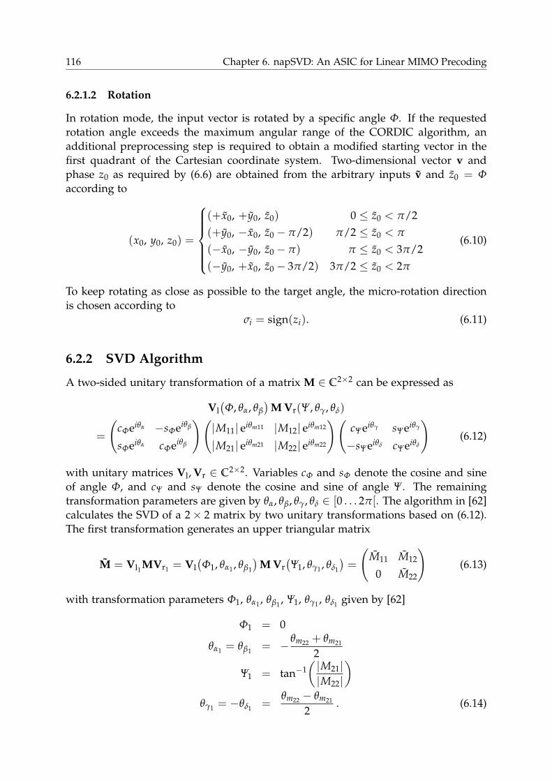
116 Chapter 6. napSVD: An ASIC for Linear MIMO Precoding
6.2.1.2 Rotation
In rotation mode, the input vector is rotated by a specific angle Φ. If the requestedrotation angle exceeds the maximum angular range of the CORDIC algorithm, anadditional preprocessing step is required to obtain a modified starting vector in thefirst quadrant of the Cartesian coordinate system. Two-dimensional vector v andphase z0 as required by (6.6) are obtained from the arbitrary inputs v and z0 = Φ
according to
(x0, y0, z0) =
(+x0, +y0, z0) 0 ≤ z0 < π/2(+y0, −x0, z0 − π/2) π/2 ≤ z0 < π
(−x0, −y0, z0 − π) π ≤ z0 < 3π/2(−y0, +x0, z0 − 3π/2) 3π/2 ≤ z0 < 2π
(6.10)
To keep rotating as close as possible to the target angle, the micro-rotation directionis chosen according to
σi = sign(zi). (6.11)
6.2.2 SVD Algorithm
A two-sided unitary transformation of a matrix M ∈ C2×2 can be expressed as
Vl(Φ, θα, θβ
)M Vr(Ψ, θγ, θδ)
=
(cΦeiθα −sΦeiθβ
sΦeiθα cΦeiθβ
)(|M11| eiθm11 |M12| eiθm12
|M21| eiθm21 |M22| eiθm22
)(cΨeiθγ sΨeiθγ
−sΨeiθδ cΨeiθδ
)(6.12)
with unitary matrices Vl, Vr ∈ C2×2. Variables cΦ and sΦ denote the cosine and sineof angle Φ, and cΨ and sΨ denote the cosine and sine of angle Ψ. The remainingtransformation parameters are given by θα, θβ, θγ, θδ ∈ [0 . . . 2π[. The algorithm in [62]calculates the SVD of a 2× 2 matrix by two unitary transformations based on (6.12).The first transformation generates an upper triangular matrix
M = Vl1MVr1 = Vl(Φ1, θα1 , θβ1
)M Vr
(Ψ1, θγ1 , θδ1
)=
(M11 M12
0 M22
)(6.13)
with transformation parameters Φ1, θα1 , θβ1 , Ψ1, θγ1 , θδ1 given by [62]
Φ1 = 0
θα1 = θβ1 = −θm22 + θm21
2
Ψ1 = tan−1(|M21||M22|
)θγ1 = −θδ1 =
θm22 − θm21
2. (6.14)

6.2. 2 x 2 SVD Algorithm and Architecture 117
The second transformation delivers a real-valued diagonal matrix
M = Vl2MVr2 = Vl(Φ2, θα2 , θβ2
)M Vr
(Ψ2, θγ2 , θδ2
)=
(M11 0
0 M22
)(6.15)
that contains the singular values of M. The corresponding transformation parametersΦ2, θα2 , θβ2 , Ψ2, θγ2 , θδ2 based on M are given by [62]
θα2 = −θm12 + θm11
2
θβ2 = θγ2 = −θδ2 =θm12 − θm11
2
tan(Φ2 ±Ψ2) = −(
|M12||M22| ∓ |M11|
). (6.16)
The complex-valued exponentials as well as the cosine and sine in (6.12) can be gen-erated by the CORDIC algorithm in rotation mode. The angular coordinates of thescalar elements in M and M, and the trigonometric functions in (6.14) and (6.16) canbe derived using a CORDIC in vectoring mode. The diagonal matrix containing thesingular values is given by
Λ = Vl2Vl1 M Vr1Vr2 . (6.17)
6.2.3 Architecture
This section describes the architecture implementing the algorithm for 2 × 2 SVDdescribed in Section 6.2.2. A core component of this architecture is the CORDICunit (Section 6.2.3.1) which is used to realize a 2 × 2 unitary transformation matrix(UTM) generator (Section 6.2.3.2). Four of these generators are required to implementthe two-step, two-sided unitary transformation that generates a 2× 2 SVD (Section6.2.3.4).
6.2.3.1 CORDIC
The CORDIC architecture template used in this work is depicted in Figure 6.2. It isdesigned to perform one CORDIC operation (i.e., vectoring or rotation) in multiplecycles, reusing the same hardware. Therefore, the elements within the template arecontrolled by an FSM and adapted to the current processing cycle. The preprocess-ing block (Prep.) implements the rotation of the input vector to the right quadrantof the Cartesian coordinate system (see (6.7), (6.10)). The preprocessed input is thenforwarded within the same clock cycle to the iterator block (IT) which executes plainCORDIC micro-rotations. The iterator block consists of a chain of iterator elementswhereof each performs a single CORDIC micro-rotation as in (6.6). The number ofiterator elements in the chain is design-time configurable. The output of the chaincan be fed back to the input multiple times (e.g., depending on numerical precisionrequirements). After finishing the iteration phase, the result is routed to the post-

118 Chapter 6. napSVD: An ASIC for Linear MIMO Precoding
Prep.
IT
Postp.x0y0z0
xLyLzL
Figure 6.2: Schematic of CORDIC unit.
processing block (Postp.) in the subsequent clock cycle. The postprocessing blockmultiplies the scalar elements of the post-iteration vector by correction factor κ ac-cording to (6.5).
The architecture template can also be design-time configured to support runtime-adaptable parameters to tune the numerical precision of the CORDIC operation tothe numerical precision requirements of the surrounding application. By doing so,switching activity in the circuit is minimized, which reduces the energy consumptionper CORDIC operation.
• Adapting CORDIC iteration cycles configures the number of micro-rotationson the granularity level of iterators in the IT block. The correction factor κ in thepostprocessing block is adapted accordingly.
• Adapting the iterator chain length by bypassing a configurable number of iter-ators adapts the number of micro-rotations on the granularity level of a singlerotation.
• A configurable bitmask, applied to a certain number of LSBs prior to eachmicro-rotation and the postprocessing unit, implements an adaptive numberformat.
6.2.3.2 2 x 2 Unitary Transformation Matrix Generation
The schematic of the UTM generator for left-hand side matrix Vl(Φ, θα, θβ) is shown inFigure 6.3. Inputs and outputs of CORDIC units are ordered according to Figure 6.2.For all following schematics, unlabeled inputs are supposed to be zeroed. The UTMgeneration circuit is divided into two coarse-grained computational stages (St.). Eachcomputational stage performs its respective task in a maximum of CS clock cyclesbefore passing the result to the next state. This means that during each time periodof CS cycles, also referred to as a computational cycle, the UTM generator performs thesame task on different data. The computation of the left-hand and right-hand unitarymatrices Vl(Φ, θα, θβ) and Vr(Ψ, θγ, θδ) in (6.12) requires the sines and cosines of Φ
and Ψ. These trigonometric functions are generated in the first computational stage bya CORDIC unit in rotation (rot.) mode, passing 1 and 0 to x0 and y0, respectively, andΦ or Ψ to z0. At the output of the CORDIC unit, the cosine and sine are available atports xL and yL. These values are then passed to the second computational stage andassigned to the real-valued components of the complex-valued inputs of four CORDIC

6.2. 2 x 2 SVD Algorithm and Architecture 119
CORDICrot.
CORDICrot.
CORDICrot.Φ
cΦ
sΦ
θα
θβ
Vl,11
Vl,12
Vl,22
Vl,21
1
−1
St.1 St.2
CORDICrot.
CORDICrot.
Figure 6.3: Schematic of left-hand side 2× 2 unitary transformation matrix (UTM)generator.
units in rotation mode, while the imaginary components are set to zero. Forwardingθα and θβ (for Vl(Φ, θα, θβ)) or θγ and θδ (for Vr(Ψ, θγ, θδ)) to the corresponding z0ports generates the desired transformation matrices.
6.2.3.3 Transformations Q1 and Q2
The 2× 2 SVD of input matrix M is realized by two transformations denoted as Q1and Q2. The corresponding hardware blocks labeled Q1 and Q2 compute the requiredUTMs.
The schematic of Q1 is illustrated in Figure 6.4. The circuit is spread across fourcomputational stages, whereof the first two (in yellow) calculate the transformationparameters from (6.14) and the last two (in turquoise) generate the UTMs. The firststage calculates amplitudes and phases of scalar components M21 and M22 of inputmatrix M, utilizing two CORDIC units in vectoring mode (vec.). From these results,the second stage computes Ψ1 based on the amplitudes of M21 and M22. Phasesθα1 and θγ1 are calculated using θm21 and θm22 according to (6.14). In the next twostages, the 2× 2 transformation matrices of Q1 are computed. Due to Φ1 = 0, thenon-diagonal parts of Vl(Φ1, θα1 , θβ1) are zero as well. Furthermore, θα1 = θβ1 meansthat the two diagonal elements are equal. Thus, the computation of Vl(Φ1, θα1 , θβ1)can be reduced to a single CORDIC operation in rotation mode. As a result, the lefttransformation matrix is already available in the third computational stage, while thecomputation of the right matrix is finished in stage four. In addition to the arithmeticoperations performed in Q1, the input matrix is stored in a first-in, first-out (FIFO)storage element that samples its input every CS-th clock cycle. The delayed value ofM is used to calculate M as in (6.13).
The structure of the Q2 architecture is shown in Figure 6.5. The parameters forUTM generation according to (6.16) are calculated in the first two computationalstages. The last two stages generate the transformation matrices themselves. The firstcomputational stage derives amplitudes and phases of the scalar elements M11, M12and M22 of matrix M. Since the operand to the tangent in (6.16) is a fraction of am-
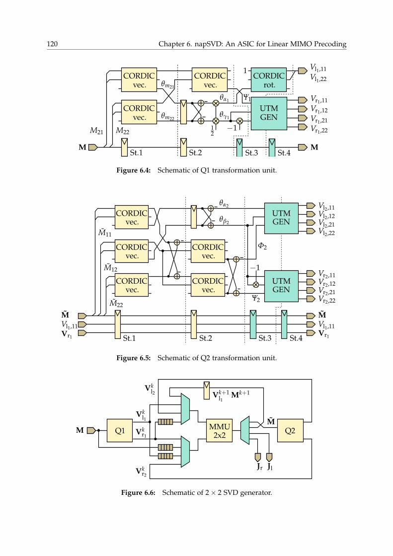
120 Chapter 6. napSVD: An ASIC for Linear MIMO Precoding
M21 M2212
θα1
1 Vl1,11
−1
Vr1,11Vr1,12Vr1,21Vr1,22
M M
θγ1
UTMGEN
St.1 St.2 St.4St.3
Ψ1
Vl1,22CORDICvec. θm21
CORDICvec. θm22
CORDICvec.
CORDICrot.
Figure 6.4: Schematic of Q1 transformation unit.
M
Vl2,11Vl2,12Vl2,21Vl2,22
−1
St.1 St.2 St.3 St.4
Vl1,11Vr1
MVl1,11Vr1
Φ2
Ψ2
M11
M12
M22
θα2
θβ2
Vr2,11Vr2,12Vr2,21Vr2,22
CORDICvec.
CORDICvec.
CORDICvec.
CORDICvec.
CORDICvec.
UTMGEN
UTMGEN
Figure 6.5: Schematic of Q2 transformation unit.
Q1 2x2
JlJr
Q2MM
Vk+1l1
Mk+1Vk
l2
Vkr2
Vkl1
Vkr1
MMU
Figure 6.6: Schematic of 2× 2 SVD generator.

6.2. 2 x 2 SVD Algorithm and Architecture 121
plitude terms, there is no need for CORDIC postprocessing in the preceding CORDICunit, because the correction factor κ cancels out. As a result, sums |M22| ∓ |M11| canbe calculated in the last cycle of the first computational stage. The second stage com-putes θα2 , θβ2 , θγ2 , and θδ2 , as well as the phases of the cosine and sine, Φ2 and Ψ2, ofthe two transformation matrices. For the latter two, the design exploits the fact thatthe phase output of the CORDIC operation does not require postprocessing, so Φ2and Ψ2 are computed in the last cycle of the second computational stage. Stages threeand four take the previously calculated parameters as inputs and generate the left andright-hand UTMs Vl(Φ2, θα2 , θβ2) and Vr(Ψ2, θγ2 , θδ2). Q2 also buffers the transforma-tion matrices generated by Q1 in a FIFO, so they can be combined with the results ofQ2 to derive the overall transformation matrices.
6.2.3.4 2 x 2 SVD
The architecture of the 2× 2 SVD block is illustrated in Figure 6.6. The 2× 2 SVDgenerator contains an instance of the Q1 and the Q2 transformation unit, and a 2× 2matrix multiplication unit (MMU) to compute M according to (6.13) and the final leftand right-hand unitary matrices
Jl(M) = Vl2Vl1 , Jr(M) = Vr1Vr2 , (6.18)
meaning the multiplication unit has to perform a total of four matrix multiplicationsper 2× 2 SVD. Allocating one cycle per matrix multiplication motivates the choice ofCS = 4, so that the 2× 2 SVD generator computes one SVD every four clock cycles. Toachieve a competitive clock frequency, the matrix multiplier has an additional pipelineregister between the real-valued scalar multipliers and the subsequent adders. Whilstincreasing the clock frequency, this pipelining introduces a potential data hazard. TheMMU has a budget of CS = 4 clock cycles to compute matrix M which is requiredas input to Q2, and for output matrices Jl and Jr (see (6.18)). Since the computationof one matrix multiplication has a latency of two clock cycles, the calculation of Malone introduces a latency of four cycles. However, Vl2 and Vr2 depend on M, soall calculations in the MMU that use these two matrices have to be scheduled afterthe calculation of M but within the same computational cycle. With a latency of fourcycles for the computation of M, this constraint cannot be fulfilled. To overcome thisissue, the design exploits the fact that Vl1 is available CS clock cycles prior to Vr1 .Consequently, the intermediate result Vl1M is computed one computational cycleprior to the computation of M and stored in a clock-gated register until it is usedin the next computational cycle. The assignments of multiplications to clock cycles iwithin computational cycle k is given by
Mout =
(Vk
l1Mk)
Vkr1
i = 1
Vk+1l1
Mk+1 i = 2
Vkl2
Vkl1
i = 3
Vkr1
Vkr2
i = 4 .
(6.19)

122 Chapter 6. napSVD: An ASIC for Linear MIMO Precoding
Algorithm 4 Cyclic Jacobi algorithm for SVD of N × N matrix [41].1: Λ← M2: V← IN3: for s ← 1 to NSW do4: for p ← 1 to N − 1 do5: for q ← p + 1 to N do6: Λ← Ja
l (p, q, Λ(p,q))Λ Jar (p, q, Λ(p,q))
7: V← V Jar (p, q, Λ(p,q))
8: end for9: end for
10: end for
The computation of matrix M, which is input to Q2, starts in the second clock cycleand is continued in the first clock cycle of the following computational cycle. Since thematrix multiplication unit contains one pipeline register, M can be used starting fromthe third clock cycle within the computational cycle. Therefore, the computationalcycles of Q2 have a two clock cycle phase offset as opposed to Q1.
6.3 N x N SVD Algorithm and Architecture
The aforementioned Jacobi method for SVD allows the computation of the SVD ofan N × N matrix based on two-sided unitary transformations. Section 6.3.1 intro-duces the underlying algorithm of the Jacobi method which is then transferred intoa representation entirely based on 2× 2 arithmetic. Section 6.3.2 describes how thepreviously introduced 2× 2 SVD architecture can be embedded into a bigger circuitwhere it is used to implement N × N SVDs. Control flow and address generationof the N × N architecture are designed to guarantee full utilization of the 2× 2 SVDunit.
6.3.1 Algorithm
The cyclic Jacobi method [41] for SVD of matrix M ∈ CN×N in its original form isshown in Algorithm 4, where IN denotes an N × N identity matrix. The singularvalues of M are computed in an iterative fashion based on 2× 2 SVDs and N × Nmatrix-matrix multiplications. To that end, the input matrix is multiplied by a series ofaugmented left and right-hand transformation matrices Ja
l and Jar . These matrices are
identity except at four positions: (p, p), (p, q), (q, p), (q, q) with p < q ≤ N. At thesefour positions, Ja
l and Jar are defined by Jl(Λ
(p,q)) and Jr(Λ(p,q)). Here, Λ(p,q) ∈ C2×2

6.3. N x N SVD Algorithm and Architecture 123
denotes a matrix composed of four elements of Λ at the aforementioned positions.The scalar elements for row i and column j of Ja
l and Jar are given by
Jal,ij
(p, q, Λ(p,q)
)=
1 i=j ∧ i 6=p ∧ j 6=q
Jl,11
(Λ(p,q)
)i=p ∧ j=p
Jl,12
(Λ(p,q)
)i=p ∧ j=q
Jl,21
(Λ(p,q)
)i=q ∧ j=p
Jl,22
(Λ(p,q)
)i=q ∧ j=q
0 else
(6.20)
Jar,ij
(p, q, Λ(p,q)
)=
1 i=j ∧ i 6=p ∧ j 6=q
Jr,11
(Λ(p,q)
)i=p ∧ j=p
Jr,12
(Λ(p,q)
)i=p ∧ j=q
Jr,21
(Λ(p,q)
)i=q ∧ j=p
Jr,22
(Λ(p,q)
)i=q ∧ j=q
0 else.
(6.21)
For each iteration s, which is also referred to as a sweep, Algorithm 4 iterates over allpairs (p, q) to update matrices Λ and V. After a sufficient number of sweeps NSW,matrix Λ contains the singular values of M on its diagonal and V converges to theprecoding matrix from (2.11).
Algorithm 4 can be optimized by exploiting the fact that a sweep over all pairs(p, q) contains N − 1 groups of N/2 pairs that can be processed in parallel withoutinterfering with each other [16]. The corresponding rearrangement of pairs (p, q) iscalled parallel ordering. The pairs can be generated in a hardware-friendly fashionby a register bank and a fixed permutation mesh between the inputs and outputs ofthe bank. The register contents are initialized with increasing integers from 1 to N.For each following clock cycle, the circuit generates a new set of independent pairs.Figure 6.7 shows the generation of all pairs for an 8× 8 SVD. The preliminary values( p, q) from the register bank have to be postprocessed according to
(p, q) =
{( p, q) p < q(q, p) q < p.
(6.22)
Using parallel ordering as in Figure 6.7 results in a cycle count of
CSW = CS(N − 1)N/2 (6.23)
per sweep which is listed in Table 6.1 for N ∈ {2, 4, 6, 8}.Since the parallel ordering pairs are disjunct, Algorithm 4 can be rewritten so
the left and right-hand multiplication matrices from Line 6 are not based on just one

124 Chapter 6. napSVD: An ASIC for Linear MIMO Precoding
(1,2) (3,4) (5,6) (7,8)
(1,4) (2,6) (3,8) (5,7)
(1,6) (4,8) (2,7) (3,5)
(1,8) (6,7) (4,5) (2,3)
(1,7) (8,5) (6,3) (4,2)
(1,5) (7,3) (8,2) (6,4)
(1,3) (5,2) (7,4) (8,6)
Figure 6.7: Pair generation of parallel ordering for 8× 8 SVD.
N 2 4 6 8
CSW 4 24 60 112
Table 6.1: Clock cycles to process one N × N SVD sweep.
pair of the current parallel ordering permutation but on all N/2 of them. This stepfacilitates a high throughput hardware implementation by enabling the computationof more transformations on the input matrix without having to wait for the resultsof previous transformations which first have to pass through the entire processingpipeline. For the disjunct pairs (pv, qv), v ∈ {1, . . . , N/2} of the current parallelordering permutation, the combined left-hand transformation matrix Jc
l ∈ CN×N is
Jcl =
N/2∑v=1
Jpl [v]
Jpl,ij[v] =
Jl,11
(Λ(pv,qv)
)i=pv ∧ j=pv
Jl,12
(Λ(pv,qv)
)i=pv ∧ j=qv
Jl,21
(Λ(pv,qv)
)i=qv ∧ j=pv
Jl,22
(Λ(pv,qv)
)i=qv ∧ j=qv
0 else .
(6.24)
Similarly, based on all disjunct pairs (pu, qu), u ∈ {1, . . . , N/2}, the combined right-hand matrix Jc
r ∈ CN×N is given by
Jcr =
N/2∑u=1
Jpr [u]
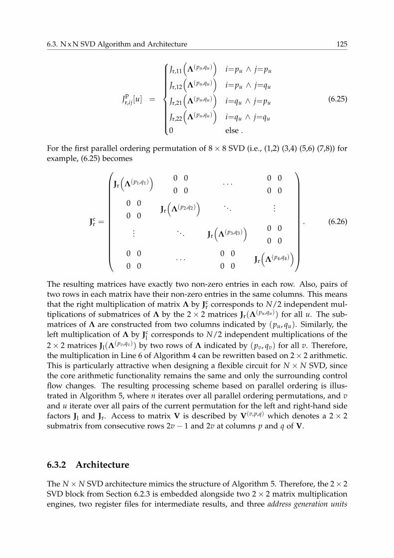
6.3. N x N SVD Algorithm and Architecture 125
Jpr,ij[u] =
Jr,11
(Λ(pu,qu)
)i=pu ∧ j=pu
Jr,12
(Λ(pu,qu)
)i=pu ∧ j=qu
Jr,21
(Λ(pu,qu)
)i=qu ∧ j=pu
Jr,22
(Λ(pu,qu)
)i=qu ∧ j=qu
0 else .
(6.25)
For the first parallel ordering permutation of 8× 8 SVD (i.e., (1,2) (3,4) (5,6) (7,8)) forexample, (6.25) becomes
Jcr =
Jr
(Λ(p1,q1)
) 0 0
0 0· · ·
0 0
0 0
0 0
0 0Jr
(Λ(p2,q2)
) . . . ...
... . . . Jr
(Λ(p3,q3)
) 0 0
0 0
0 0
0 0· · ·
0 0
0 0Jr
(Λ(p4,q4)
)
. (6.26)
The resulting matrices have exactly two non-zero entries in each row. Also, pairs oftwo rows in each matrix have their non-zero entries in the same columns. This meansthat the right multiplication of matrix Λ by Jc
r corresponds to N/2 independent mul-tiplications of submatrices of Λ by the 2× 2 matrices Jr(Λ(pu,qu)) for all u. The sub-matrices of Λ are constructed from two columns indicated by (pu, qu). Similarly, theleft multiplication of Λ by Jc
l corresponds to N/2 independent multiplications of the2× 2 matrices Jl(Λ
(pv,qv)) by two rows of Λ indicated by (pv, qv) for all v. Therefore,the multiplication in Line 6 of Algorithm 4 can be rewritten based on 2× 2 arithmetic.This is particularly attractive when designing a flexible circuit for N × N SVD, sincethe core arithmetic functionality remains the same and only the surrounding controlflow changes. The resulting processing scheme based on parallel ordering is illus-trated in Algorithm 5, where n iterates over all parallel ordering permutations, and vand u iterate over all pairs of the current permutation for the left and right-hand sidefactors Jl and Jr. Access to matrix V is described by V(v,p,q) which denotes a 2× 2submatrix from consecutive rows 2v− 1 and 2v at columns p and q of V.
6.3.2 Architecture
The N×N SVD architecture mimics the structure of Algorithm 5. Therefore, the 2× 2SVD block from Section 6.2.3 is embedded alongside two 2× 2 matrix multiplicationengines, two register files for intermediate results, and three address generation units

126 Chapter 6. napSVD: An ASIC for Linear MIMO Precoding
Algorithm 5 Jacobi algorithm with parallel ordering for SVD of N × N matrix.1: Λ← M2: V← IN3: for s ← 1 to NSW do4: for n ← 1 to N − 1 do5: Compute next set of pairs (p1, q1), .., (pN/2, qN/2)6: for u ← 1 to N/2 do7: for v ← 1 to N/2 do8: Λ(pv,qu) ← Jl(Λ
(pv,qv))Λ(pv,qu)Jr(Λ(pu,qu))9: V(v, pu,qu) ← V(v, pu,qu)Jr(Λ(pu,qu))
10: end for11: end for12: end for13: end for
(AGUs) to direct the required data from the register files to the computational unitsand feed the results back to the register files.
6.3.2.1 Functional Units Overview
The structure of the N × N SVD architecture implementing Algorithm 5 is shown inFigure 6.8. In the following, the main components are introduced. The IO register file(IO reg) acts as a local cache. It is accessible from the outside to write the input matri-ces M and read out the result, once M has been iteratively transformed to Λ. To theinside, it provides 2× 2 submatrices of the current version of Λ as input to the 2× 2SVD block to compute Jl(Λ
(pv,qv)) and Jr(Λ(pu,qu)). It also provides Λ(pv,qu) to the Λ
multiplication engine (Λ mul). The result produced by the multiplication engine (i.e.,the left side of Algorithm 5, Line 8) is fed back to the IO register file to update the Λ-matrix. After all sweeps have been processed, the register file contains the final matrixΛ which has been diagonalized and whose entries now hold the singular values of M.To match the access pattern of Algorithm 5, the register file accepts four scalar inputsand delivers four scalar outputs per clock cycle. The storage elements are organized ina two-dimensional grid, whereof two rows can be addressed simultaneously via tworow indices. Out of these two rows, two columns are selected by two column indices.Trial synthesis and layout runs show that the resulting multiplexing and demultiplex-ing complexity is significant enough to prolong the critical path. Therefore, there is anadditional pipeline register in front of the demultiplexing network from the input ofthe register file to the actual storage cells. Also, all computational elements connectedto the output of the IO register file have their inputs directly connected to a pipelineregister so there is a sufficient time budget for the multiplexing network at the outputof the IO register file. Additional pipeline registers are inserted at the same positionsin the register file holding matrix V.
The access pattern described by the two for-loops in Line 6 and 7 of Algorithm 5can only be realized if all N/2 matrices Jl and Jr of the current parallel ordering

6.3. N x N SVD Algorithm and Architecture 127
IO regSVD 2x2
Jl bufΛ mul
Jr buf
IO-SVDAGU
IO-Λ mulAGU
addr. out
addr. inda
taou
t
data
in V mul V reg
V reg-V mulAGU
Figure 6.8: Schematic of N × N SVD generator.
permutation have been computed. However, the 2 × 2 SVD block computes thesematrices successively. Therefore, two buffers (Jl buf, Jr buf) are placed in front of theΛ multiplication engine. They delay the computation of Line 8 until the 2× 2 SVDblock has delivered enough matrices Jl and Jr of the current parallel ordering permu-tation, so that the Λ multiplication engine can run at the highest possible utilization.The third input to the multiplication engine is matrix Λ(pv,qu), the middle-factor fromAlgorithm 5, Line 8. In case of v = u, this input comes from the 2× 2 SVD enginethrough which it passed via a FIFO. This data cannot be obtained directly from the IOregister file, since the register file has to provide the next input to the 2× 2 SVD blockin the same clock cycle. For all remaining clock cycles of the current computationalcycle, the SVD block requires no additional inputs from the IO register file, so theregister file can supply data to the Λ multiplication engine directly.
The V multiplication engine (V mul) generates the N × N precoding matrix Vfrom the 2× 2 output matrices Jr of the 2× 2 SVD block. The computation followsLine 9 of Algorithm 5. The intermediate version of the precoding matrix is stored inthe V register file (V reg). Since Algorithm 5 operates on consecutive rows of V, theregister file can be simplified as opposed to the Λ register file. While still providingrandom access to two columns, the row-access is now controlled by a single addressso that the content of one row in the register file matches two consecutive rows ofmatrix V. The corresponding AGU computes the output addresses of the V registerfile for the intermediate matrices V(v, pu,qu) which are forwarded as left-hand inputsto the V multiplication engine. The right-hand inputs come directly from the outputof the 2× 2 SVD block.
6.3.2.2 Control Flow & Address Generation
The control flow of the N × N SVD block is mainly defined by the way the designsteps through the loops in Algorithm 5 and the corresponding accesses patterns tothe IO register file. In addition to the flow presented in Algorithm 5, the hardwareimplementation also interleaves the processing of a certain number of matrices to en-

128 Chapter 6. napSVD: An ASIC for Linear MIMO Precoding
able full utilization of the 2 × 2 SVD pipeline. The overall access pattern and thecorresponding address generation is composed of a number of nested control loopsthat are introduced in the following from the inside to the outside of the loop hierar-chy of Algorithm 5.
• Serial access control refers to the serialization of parallel ordering permutationsso data can be transferred from and to the Λ and V register files whose interfacesare designed for a single 2× 2 matrix per access.
• Matrix access control decides which of the input matrices in the IO register fileis processed. Every time one serial access cycle is completed, the control flowswitches to the next matrix where the same serial access pattern with the sameparallel ordering permutation is used. For the address generation, an offsetcorresponding to the number of rows of one input matrix is added to the rowaddresses.
• Parallel access control manages the iteration through the parallel ordering per-mutations. Once all serial accesses of the current parallel ordering permutationhave been used on all matrices, the next parallel ordering permutation is gener-ated.
• Sweep control keeps track of what sweep the architecture is in to know when theSVD computation is finished. It does not impact the actual address generation,since each sweep operates on the same addresses. After completion, the designswitches into an IO state, in which the IO register file is accessible from thedesign boundary, so results can be read out and the matrices for the next set ofSVDs can be written in.
Different AGUs have different serial access control flows, as can be seen by thedifferent indexing schemes on the parallel ordering permutation pairs in Line 8 and 9of Algorithm 5. The remaining control of all AGUs is identical, though. The IO-SVDAGU generates the access pattern for the 2× 2 matrix input to the 2× 2 SVD block.Serial access control selects a pair from one single parallel ordering permutation unitin a cyclic fashion. Since the SVD block expects a new input every CS clock cycles,the IO-SVD AGU is clock-gated so the serial access control proceeds only every CS-thclock cycle. The IO-Λ mul AGU generates the addresses for matrices Λ(pv,qu) in Line 8of Algorithm 5. Note that pair (pv, qu) contains two different indexing schemes. Thus,serial access control iterates through all combinations of u and v from Algorithm 5.The sequence of u and v is selected to minimize the latency introduced by the buffer-ing between the SVD block and the multiplication engine. The generated addressesare buffered in a FIFO and used later to write back the result of the multiplication inLine 8. Serial access control of the V reg-V mul AGU iterates through a single set ofparallel ordering permutations that generate one pair (pu, qu) every CS clock cycles.For each pair, the row-counter v advances until the pu-th and qu-th column of thecurrent matrix have been processed completely.

6.3. N x N SVD Algorithm and Architecture 129
6.3.2.3 Latency Analysis and Circuit Dimensioning
To efficiently utilize the N × N SVD architecture, all computational stages should bekept busy at all times. Since Algorithm 5 performs SVD in an iterative fashion, theresult of one iteration has to be computed by the 2× 2 SVD unit and the multiplicationengines, and then be written back to the IO register file before the next iteration canstart. Parallel ordering allows the independent processing of N/2 SVDs of size 2× 2without updating the input matrix. However, the architecture in Figure 6.8 consistsof more than N/2 computational stages, which means that the design cannot be fullyutilized when operating on one input matrix only. This problem can be mitigated byprocessing MI input matrices in an interleaved scheme, as indicated in Section 6.3.2.2.Since handling a bigger number of matrices results in increased storage requirementsfor both register files, it is desirable to reduce interleaving to the smallest degreethat enables maximum utilization of all functional units. To that end, the previouslyintroduced architecture and its data flow have to be analyzed with respect to latency(i.e., the total number of computational stages). The 2× 2 SVD block itself causes alatency of nine computational cycles; four from Q1, another four from Q2, and onefrom the matrix multiplier. The buffering of Jl and Jr causes an additional latencyof two computational cycles. Finally, the two cascaded matrix multipliers in the Λ
multiplication engine cause another delay corresponding to one computational cycle.Therefore, the overall latency of the processing pipeline equals LT = 12 computationalcycles, meaning the processing pipeline has to be fed with at least LT + 1 inputs for2 × 2 SVD calculation before operating again on the first input matrix. Since eachparallel ordering permutation contains N/2 independent pairs, the number MI ofinterleaved matrices has to satisfy
MI ≥⌈
2(LT + 1)N
⌉=
⌈26N
⌉. (6.27)
Based on (6.27), the storage requirement in terms of complex-valued scalars is
SI = MIN2 =
⌈2(LT + 1)
N
⌉N2 =
⌈26N
⌉N2. (6.28)
In line with the IEEE 802.11ac [72] standard, 8× 8 MIMO is defined as the maximumantenna setup and the N × N SVD template is configured accordingly. The results ofMI and SI for N ∈ {2, 4, 6, 8} are summarized in Table 6.2. The data shows that N = 8has the highest storage requirements, so the IO register file is designed to hold four8× 8 matrices arranged in 32 rows and 8 columns.
Next, the multiplication engines for Λ and V are dimensioned so they can han-dle the throughput generated by the 2× 2 SVD block which always operates at fullutilization. Based on Algorithm 5, there are
Mppmul = N2/4 (6.29)

130 Chapter 6. napSVD: An ASIC for Linear MIMO Precoding
Dimension: N Matrices: MI Storage: SI
2 13 524 7 1126 5 1808 4 256
Table 6.2: Storage requirements of interleaved N × N SVD with N ∈ {2, 4, 6, 8}.
Antenna setup 2× 2 4× 4 6× 6 8× 8
CORDIC iterations 4 5 5 6Scalar wordwidth 10 12 12 13Number of sweeps 1 2 2-3 3-4
Table 6.3: Numerical precision requirements for SVD precoding.
three-factor matrix multiplications required per parallel ordering permutation. Thematrix factors stem from N/2 SVDs of size 2× 2, each taking CS = 4 cycles to com-pute. Thus, the 2× 2 SVD block has a total execution cycle count of
Cppsvd = 2N (6.30)
for one parallel ordering permutation. For the multiplication engine to match thethroughput of the SVD block, it has a cycle budget of
Cppmul =
Cppsvd
Mppmul
=8N
(6.31)
per two-sided matrix multiplication which is one for the maximum use case of N = 8.This means the multiplication engine has to be designed to deliver a throughput ofone three-factor matrix multiplication per clock cycle. Therefore, the Λ multiplicationengine is composed of two cascaded matrix multiplication units whereof the secondtakes the output of the first as its left-hand input. The same argumentation appliesto the dimensioning of the V multiplication engine with respect to one-sided matrixmultiplications, so the corresponding block contains a single pipelined 2× 2 matrixmultiplier.

6.4. Numerical Precision Analysis 131
6.4 Numerical Precision Analysis
This section discusses the numerical precision requirements of N× N SVD precodingusing the napSVD architecture for N ∈ {2, 4, 6, 8}. The results are summarized inTable 6.3. The maximum requirements are considered achieved when the communi-cation performance (i.e., FER) of the napSVD architecture is indistinguishable fromthe performance delivered by the reference implementation presented in Chapter 3,using double precision floating-point arithmetic. The napSVD architecture has threeconfiguration parameters for numerical precision: number of sweeps, scalar word-width, and number of CORDIC iterations. All three influence energy consumptionand FER. Reducing CORDIC iterations and scalar wordwidth below the configura-tion for floating-point equivalence causes significant FER-impairments while offeringcomparably small reductions of energy consumption. Therefore, both parameters arefixed to the use case requirements in Table 6.3. In contrast, the number of sweeps isdirectly proportional to energy consumption, so the more attractive trade-off of en-ergy consumption and FER when altering NSW is considered in the following. To thatend, Figures 6.9a to 6.9c show the FERs of 4× 4, 6× 6 and 8× 8 antenna setups for avarying number of sweeps1. The frame structure conforms with the IEEE 802.11ac [72]standard with an up-front block preamble. The number of information bits per framecorresponds to the maximum MSDU size in IEEE 802.11 [71] (excluding the direc-tional multi-gigabit (DMG) beamforming mode of IEEE 802.11ad [70]). All setups useLDPC channel coding according to IEEE 802.11 [71] for the highest codeword lengthof 1944 bit, the highest code rate of 5/6 and the densest symbol constellation alpha-bet: 256-QAM. MIMO detection is performed by a low-complexity open-loop linearMMSE algorithm (see Section 2.4.2.1).
The analysis shows that the precision requirement in terms of sweeps changesbetween antenna configurations but also within a single configuration when using adifferent number of eigenmodes/streams MS. For a 4× 4 transmission, two sweepsdeliver double floating-point equivalent communication performance. For a targetFER of 1 %, the offset when using one sweep is around 3 dB when using all foureigenmodes and circa 1.4 dB and 0.7 dB for three or two eigenmodes, respectively. A6× 6 transmission requires three sweeps for floating-point equivalent communicationperformance for MS ∈ {5, 6}, and two sweeps otherwise. For MS = 5, switching fromthree sweeps to two causes a degradation of 0.7 dB. For MS = 6, the gap for switchingfrom three sweeps to two is significantly larger: around 3 dB. Applying one sweeponly is not even feasible, since the target FER is not achieved for realistic SNR val-ues. The 8× 8 setup needs four sweeps for floating-point equivalent communicationperformance at MS = 8 and three sweeps when using less eigenmodes. The gap incommunication performance when using two sweeps instead of three varies from analmost negligible degradation for small MS up to a 1.3 dB offset for seven modes.When reducing further to one sweep, the gap widens to slightly above 1 dB for smallMS via 4 dB for seven eigenmodes up to an impractically high SNR for eight modes.
1 For N = 2, there can be only one sweep, so 2× 2 MIMO is excluded from this examination.

132 Chapter 6. napSVD: An ASIC for Linear MIMO Precoding
16 18 20 22 24 26 28 30 32 34 36 38 40 4210−3
10−2
10−1
100
MS=2 MS=3 MS=4
FER
(a) MT = MR = 4
16 18 20 22 24 26 28 30 32 34 36 38 40 4210−3
10−2
10−1
100
MS=3 MS=4 MS=5 MS=6
FER
(b) MT = MR = 6
16 18 20 22 24 26 28 30 32 34 36 38 40 4210−3
10−2
10−1
100
MS=4 MS=5 MS=6 MS=7 MS=8
SNR
FER
NSW: 1 2 3 4
(c) MT = MR = 8
Figure 6.9: Impact of number of sweeps on FER. Modulation: 256-QAM. OFDMtones: 64. OFDM data tones: 52. Frame size: 2,304 byte (uncoded).Channel coding: LDPC, codeword length 1944 bit, code rate: 5/6. Chan-nel model: slow fading.

6.5. Implementation Results 133
1.4 1.6 1.8 2320
330
340
350
360
Tclk [ns]
Har
dwar
eco
mpl
exit
y[k
GE]
(a) Hardware efficiency.
1.4 1.6 1.8 20.9
0.92
0.94
0.96
0.98
1
Tclk [ns]En
ergy
per
cycl
e[n
J]
(b) Energy efficiency.
Figure 6.10: 8 × 8 napSVD synthesis results (90 nm CMOS, 1 V supply voltage).Wordwidth of real-valued scalar: 13 bit. Wordwidth of angular value:12 bit.
f Tclk f A
clk f Eclk AT
GE AAGE AE
GE
769 769 556 358.7 358.7 327.5
Table 6.4: Clock frequency fclk [MHz] and area A [kGE] for different design pointsusing 90 nm CMOS with 1 V supply voltage.
6.5 Implementation Results
The architecture described in Section 6.3.2 was synthesized and layouted for a 90 nmCMOS technology with 1 V supply voltage. The wordwidth was chosen according tothe maximum precision requirements for the SVD of an 8× 8 matrix, meaning 13 bitper real-valued scalar inside the IO register file (wordwidth reduces for certain func-tional units within the ASIC) and 12 bit per angular value. Synthesis was performedin topographical mode for varying clock periods Tclk. Figure 6.10a shows the result-ing hardware complexity as a function of Tclk. Figure 6.10b displays the energy perclock cycle consumed by the post-synthesis model when executing 8× 8 SVDs withfull precision. In line with the analysis in Section 5.5.1, these post-synthesis results areused to identify the clock frequencies f T
clk, f Aclk and f E
clk as well as hardware complex-ities AT
GE, AAGE and AE
GE for maximum architectural throughput, hardware efficiencyand energy efficiency. The results are summarized in Table 6.4.

134 Chapter 6. napSVD: An ASIC for Linear MIMO Precoding
Functional unit kGE % mW %
SVD 2x2 133.0 37.1 383.0 49.7Λ mul 70.5 19.7 205.0 26.6IO reg 70.2 19.6 55.4 7.2V mul 26.1 7.3 63.7 8.3V reg 44.0 12.3 21.7 2.8Misc 14.9 4.2 41.2 4.8
Total 358.7 770.0
Table 6.5: Breakdown of hardware complexity and post-layout power consumptionof the 8× 8 napSVD architecture for fclk = 752 MHz (90 nm CMOS, 1 Vsupply voltage).
The post-synthesis design achieves a maximum clock frequency of 769 MHz. Incontrast to the napCore presented in Chapter 5, this design point coincides with theone for maximum hardware efficiency. This finding can be explained by the fact thatthe napSVD design is register heavy (see Table 6.5), since it contains two tailoredregister files for inplace calculation of singular values and precoding matrices. Also,the 2× 2 SVD subdesign contains several FIFO buffers for intermediate results (seeFigures 6.4, 6.5, 6.6). Even though registers make up a significant share of the overallhardware complexity, their complexity does not grow for higher clock frequencies.Therefore, hardware efficiency is maximized for high clock frequencies. Regardingenergy consumption, all observed design points vary by less than 5 %. In summary,the design point for maximum throughput also delivers the highest hardware ef-ficiency, and energy efficiency only varies insignificantly for different frequencies.Thus, fclk = f T
clk is the design point of interest and all remaining investigations of thenapSVD architecture in this work are conducted for this clock frequency.
To prove the feasibility of the proposed design, the napSVD architecture was lay-outed at the design point for maximum throughput. Figure 6.11 shows the resultinglayout with an overlay of the physical view with the borders between functional units.The post-layout design achieves a clock frequency of 752 MHz. The design footprintis 1219 µm by 1214 µm including - and 1159 µm by 1154 µm excluding power rings,which results in a die area of 1.48 mm2 and a standard cell area of 1.34 mm2. For in-creased accuracy, all following assessments of energy efficiency are conducted basedon the post-layout model.
Table 6.5 provides a breakdown of power consumption and hardware complexityof the napSVD architecture when performing 8× 8 SVD. The 2× 2 SVD accelerator isthe most significant source of power consumption (49.7 %), followed by the two 2× 2matrix multiplication engines for Λ and V matrices (26.6 and 8.3 %). Despite a signif-icant share of 19.6 and 12.3 % in hardware complexity, the IO and V-matrix registerfiles only consume 7.2 and 2.8 % of the overall power. Even though the two regis-

6.5. Implementation Results 135
IO reg
V reg
J regJ reg
V mul
SVD 2x2
napSVD
Λ mul
Figure 6.11: Layout of the 8× 8 napSVD architecture in 90 nm CMOS with 1 V sup-ply voltage.
ter files have the exact same storage capacity, the IO variant has a higher hardwarecomplexity than the V-matrix register file. The underlying cause is the more complexaddressing scheme of the IO register file that allows reading and writing of a 2× 2submatrix specified by two row-indices and two column-indices. This requires a morecomplex multiplexing and demultiplexing network than for the V-matrix register filewhich provides random column access but always delivers data from two adjacentrows. Figure 6.11 also identifies the IO register file as a hotspot of routing congestion.There is a high wiring density up to the topmost wiring layer shown in turquoise.This finding corresponds with the observations made regarding the napCore layout(see Section 5.6.2), underlining the importance of register file design that is often un-derestimated when architectural exploration is performed up to gate-level, only. Toachieve the competitive clock frequency of the napSVD, for example, the multiplexingand demultiplexing logic of both register files in the design has to be pipelined, asmentioned in Section 6.3.2.1.
6.5.1 Use Case Energy Benchmark
This section assesses the power and energy consumption of the napSVD architecturewhen executing different use cases. The analysis is based on the precision require-ments from Table 6.3 for 2 × 2, 4 × 4, 6 × 6 and 8 × 8 SVD precoding. Table 6.6presents power consumptions Psvd
2×2, PmulΛ , Pmul
V and PΣ of the 2× 2 SVD block, themultiplication engines to generate matrices Λ and V, and the overall napSVD design.Furthermore, the energy Esw per sweep and the energy Eclk per cycle are listed. Theenergy is derived from a time-based power analysis in Synopsys® PrimeTime®, based

136 Chapter 6. napSVD: An ASIC for Linear MIMO Precoding
Psvd2×2 Pmul
Λ PmulV PΣ Esw Eclk
[mW] [mW] [mW] [mW] [nJ] [nJ]
2× 2 318 - - 402 2.14 0.5344× 4 363 104 36.1 595 19.0 0.7916× 6 367 155 48.1 673 53.7 0.8958× 8 383 205 63.7 770 115 1.027
Table 6.6: Power and energy benchmark of SVD precoding use cases on post-layoutnapSVD model with fclk = 752 MHz for N ∈ {2, 4, 6, 8} using 90 nm CMOSand 1 V supply voltage.
on a simulation of the post-layout netlist with realistic stimuli from the simulationtestbed presented in Chapter 3.
There is a significant drop of 175 mW in power consumption when switchingfrom 8 × 8 down to the 4 × 4 antenna configuration. Several factors contribute tothis behavior. First, the 6× 6 and 4× 4 configuration can operate numerically stablewith less CORDIC iterations and a smaller wordwidth than the 8× 8 setup (see Table6.3). This allows to employ NAP to reduce power consumption. The strong reductionin power consumption for the multiplication units (i.e., 49 % for the calculation ofΛ comparing N = 8 and N = 4) also results from the multiplicative calculationscheme for Λ and V shown in Algorithm 5. While the 2× 2 SVD accelerator is alwaysoperating under full load, the utilization of the multiplication engines depends on thesize of the input matrix. Table 6.6 also compares the energy consumption per SVDsweep among different matrix sizes. Due to the difference in cycle counts per sweepand in base power consumption, one sweep for an 8× 8 matrix consumes around sixtimes more energy than for 4× 4. Considering that a 4× 4 SVD requires up to twosweeps, and an 8× 8 SVD demands up to four sweeps, the total energy per SVD isup to 12 times higher for the 8× 8 use case than for 4× 4.
6.5.2 Comparison with State-of-the-Art
This section puts the napSVD design into perspective by comparing it with otherSVD architectures from the literature. For a fair comparison, all designs are scaled to90 nm CMOS technology and a supply voltage of 1 V. Table 6.7 gives an overview ofall designs and their respective performance metrics. It should be noted that energyconsumption is difficult to compare among different works due to different imple-mentation levels and simulation approaches. For this reason, Table 6.7 only listsenergy for works based on tape-outs or with a detailed description of how the resultswere obtained2.2 The variance of simulated energy consumption is significant among different simulation approaches.
To demonstrate this effect, the energy consumption of the napSVD design was evaluated using asimple but common approach based on fixed toggle rates at the input ports. These toggle rates are

6.5. Implementation Results 137
The matrix decomposition units MDU1 and MDU2 presented in [102] computethe SVD or QR factorization of 4 × 4 matrices. SVD is performed based on theGolub-Kahan (GK) algorithm [44]. Both, bidiagonalization and diagonalization areexpressed entirely based on Givens rotations. The slim core arithmetic unit consistsof one two-dimensional CORDIC unit and one multiply-accumulate unit only. Themain difference between MDU1 and MDU2 is that the latter can adapt the numberof CORDIC micro-rotations at runtime. In 180 nm CMOS, MDU1 and MDU2 have asmall size of 42.3 and 38.1 kGE at a clock frequency of 133 and 272 MHz, respectively.The small hardware complexity per MDU is penalized by a high cycle count of 1,539and 4,306 per SVD. For 4× 4 MIMO, the napSVD architecture has a significant ad-vantage in hardware efficiency of a factor of 10.7 and 13.2 over MDU1 and MDU2.Similar results are obtained for energy efficiency where the napSVD has an advantageof 15.0 and 13.6 over MDU1 and MDU2. In the light of this significant gap, it shouldbe mentioned that the napSVD architecture in its current configuration does not sup-port QR factorization. The architecture in [99] is based on [102] but tailored to SVDonly. As in [102], the supported input matrix size is 4× 4. The more tailored designapproach allows to improve the hardware efficiency significantly. Still, the napSVDhas an efficiency advantage factor of 3.1 over [99], in addition to supporting multi-ple matrix dimensions efficiently. Also, the results from [99] are given post-synthesisand no energy estimates are provided. One contribution to the efficiency advantageof the napSVD over [99, 102] comes from its beneficial numerical properties. Evenfor 8× 8 MIMO, the two-sided Jacobi scheme from Algorithm 5 operates numericallystable on a 13-bit fixed-point data format using CORDIC units with a maximum of sixmicro-rotations. The GK-based designs in [99, 102], on the other hand, contain mem-ory with 16-bit per real-valued scalar, and [99] mentions that the internal wordwidthwidens up to 19 bit. Also, the design in [99] requires nine CORDIC micro-rotationsfor numerically stable operation.
The authors of [129] use a systolic array for generalized triangular decomposition(GTD) with SVD as a special case for up to 8 × 8 MIMO. Inefficiencies associatedwith systolic arrays [99,102], particularly hardware underutilization, give the napSVDarchitecture a 25-fold advantage in terms of area efficiency for 8× 8 channel matrices.Since [129] supports smaller size matrices by disabling processing elements in thearray, the napSVD, that always full utilizes its core 2× 2 SVD unit, has a 100-fold areaefficiency advantage for 4× 4 MIMO.
The design from [130] computes SVDs of matrices up to size 4 × 4. The un-derlying algorithm called SL-SVD (superlinear convergence) relies on the orderedsingular values λ1 ≥ λ2 ≥ λ3 ≥ λ4 being different enough so that the relationλn
1 � λn2 � λn
3 � λn4 is fulfilled for a sufficiently high n ∈ N. This assumption
then propagated through the design and switching activity is derived accordingly. This approachdelivered an energy consumption 20 times lower than the results obtained from the setup describedin Section 6.5.1. Even for taped-out designs like the MIMO detector from [103], a change of stimulialone caused a sixfold difference in energy consumption.

138 Chapter 6. napSVD: An ASIC for Linear MIMO Precoding
is required because the further derivation requires that the n-fold self-multiplicationP(n) of P(0) = HH
a Ha can be approximated by
P(n) = P(n−1)P(n−1) =
MT∑i=1
λ2n+1
i vivHi ≈ λ2n+1
1 v1vH1 . (6.32)
The authors performed simulations for one channel scenario and claim that n = 8is sufficient. All further efficiency assessments are based on that claim. It must bekept in mind that the choice of n is highly dependent on the channel characteristicsand will be higher if the singular values lie closer together. This becomes more andmore problematic for bigger size channel matrices. In the corner case for two or moresingular values being equal, the algorithm never converges. A channel with equalsingular values is the optimal case that maximizes channel capacity [113], though.The aforementioned assumption buys the design in [130] an advantage of 25 % overthe napSVD in terms of area efficiency for 4× 4 SVD.
ASIP design [80] provides an interesting comparison with a programmable solu-tion. The architecture of [80] is rather generic with a data path composed of fourfloating-point units for multiplication and addition, and four accelerators for squareroot calculation. Similar to the napSVD architecture, the ASIP also has the versatilityto compute SVDs of different size matrices. However, in the case of ASIP [80], thisversatility is penalized by a high execution time. Therefore, the napSVD has a 188-fold advantage in area efficiency over [80] for 8× 8 SVD. This significant ASIC-ASIPefficiency gap3 points to the fact that efficient SVD computation requires more spe-cialized hardware and a suitable architecture should at least support certain trigono-metric functions (e.g., implemented by CORDIC units).
3 For comparison: the highly optimized MMSE-PIC architecture [103] only has a threefold advantageover the napCore ASIP (presented in Chapter 5) in terms of hardware efficiency.
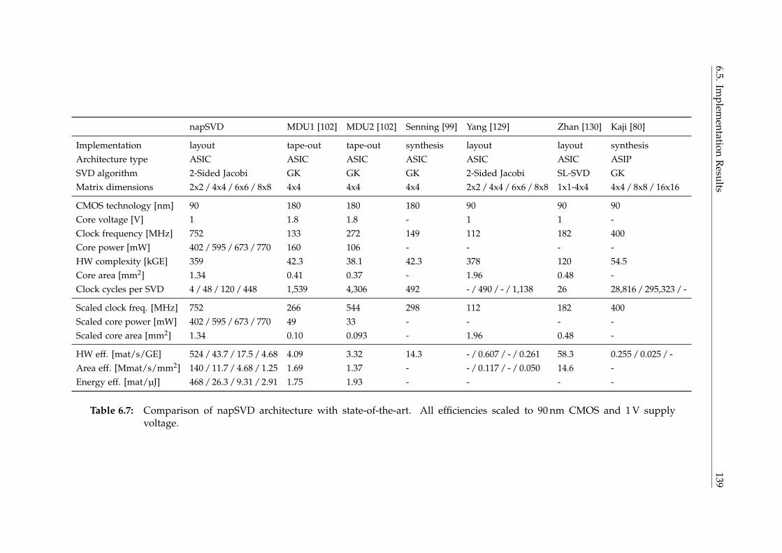
6.5.Implem
entationR
esults139
napSVD MDU1 [102] MDU2 [102] Senning [99] Yang [129] Zhan [130] Kaji [80]
Implementation layout tape-out tape-out synthesis layout layout synthesisArchitecture type ASIC ASIC ASIC ASIC ASIC ASIC ASIPSVD algorithm 2-Sided Jacobi GK GK GK 2-Sided Jacobi SL-SVD GKMatrix dimensions 2x2 / 4x4 / 6x6 / 8x8 4x4 4x4 4x4 2x2 / 4x4 / 6x6 / 8x8 1x1-4x4 4x4 / 8x8 / 16x16
CMOS technology [nm] 90 180 180 180 90 90 90Core voltage [V] 1 1.8 1.8 - 1 1 -Clock frequency [MHz] 752 133 272 149 112 182 400Core power [mW] 402 / 595 / 673 / 770 160 106 - - - -HW complexity [kGE] 359 42.3 38.1 42.3 378 120 54.5Core area [mm2] 1.34 0.41 0.37 - 1.96 0.48 -Clock cycles per SVD 4 / 48 / 120 / 448 1,539 4,306 492 - / 490 / - / 1,138 26 28,816 / 295,323 / -
Scaled clock freq. [MHz] 752 266 544 298 112 182 400Scaled core power [mW] 402 / 595 / 673 / 770 49 33 - - - -Scaled core area [mm2] 1.34 0.10 0.093 - 1.96 0.48 -
HW eff. [mat/s/GE] 524 / 43.7 / 17.5 / 4.68 4.09 3.32 14.3 - / 0.607 / - / 0.261 58.3 0.255 / 0.025 / -Area eff. [Mmat/s/mm2] 140 / 11.7 / 4.68 / 1.25 1.69 1.37 - - / 0.117 / - / 0.050 14.6 -Energy eff. [mat/µJ] 468 / 26.3 / 9.31 / 2.91 1.75 1.93 - - - -
Table 6.7: Comparison of napSVD architecture with state-of-the-art. All efficiencies scaled to 90 nm CMOS and 1 V supplyvoltage.
140 Chapter 6. napSVD: An ASIC for Linear MIMO Precoding
6.6 Discussion
Recent wireless standards like IEEE 802.11ac [72] wireless LAN define new transmis-sion setups (e.g., 8× 8 MIMO, 256-QAM, 5/6 code rate) to achieve high data rates.MIMO precoding at the transmitter is a key method to realize these data rates at rea-sonable SNRs. At the same time, precoding for lower throughput modes (e.g., lesstransmit and receive antennas) should be supported equally efficiently. This chapterdiscussed the napSVD ASIC architecture targeting SVD-based linear MIMO precod-ing. Even though designed as an ASIC for high throughput applications like IEEE802.11ac [72], the algorithmic and architectural focus of the napSVD design is on ver-satility. To that end, the entire SVD was reformulated based on 2× 2 vector arithmeticoperations that can be combined to form SVDs of bigger size matrices by applicationof the two-sided Jacobi method [41]. Therefore, the main computational units are oneCORDIC based 2× 2 SVD accelerator and two 2× 2 matrix multiplication engines.The 2 × 2 data path is mostly controlled by address generation units that employparallel ordering [16]. Parallel ordering generates the memory addresses of 2× 2 sub-matrices of the full-size matrix which the two-sided Jacobi algorithm can operate onindependently without data dependencies. At the same time, parallel ordering is eas-ily implementable by a single register and a simple permutation network. However,realizing the required access schemes to the input matrix requires a register file thatsupports addressing of a 2× 2 submatrix by the respective row and column indices.The data access schemes are repeated on the same input data for multiple iterations,referred to as sweeps, until the result converges to the actual SVD. To adapt to thenumerical precision requirements of different matrix sizes, additional measures foradaptive numerical precision were taken. The napSVD is configurable in terms offixed-point wordwidth, number of CORDIC iterations in the 2× 2 SVD accelerator,and number of conducted sweeps. The resulting architecture has a hardware com-plexity of 359 kGE and achieves a clock frequency of 752 MHz using a 90 nm CMOStechnology with 1 V supply voltage. As a proof-of-concept, a layout was conducted,occupying 1.34 mm2 of standard cell area.
Numerical precision requirements for 2× 2, 4× 4, 6× 6 and 8× 8 MIMO in termsof wordwidth, CORDIC iterations and sweeps were evaluated by extensive Monte-Carlo simulations. Additionally, it was explored how the number of sweeps can beused to trade communication performance in terms of low frame error rate againstenergy efficiency—an investigation that will be continued in-depth in Chapter 7. Thistrade-off is particularly attractive, since the energy consumption per SVD is directlyproportionally to the number of sweeps, while often, the loss in communication per-formance when using less sweeps is tolerable. Execution times per sweep are 4, 24, 60and 112 clock cycles for 2× 2, 4× 4, 6× 6 and 8× 8 complex-valued input matrices.The maximum number of required sweeps is one, two, three and four for the abovematrix sizes. The resulting area efficiencies are 140, 11.7, 4.68 and 1.25 million SVDcalculations per second and square millimeter of silicon area. Energy efficiency wasevaluated based on the post-layout model and found to be 468, 26.3, 9.31 and 2.91matrices per microjoule.

6.6. Discussion 141
These efficiencies were used for a comparison of the napSVD architecture withother state-of-the-art complex-valued SVD implementations from the literature, mostof which are tailored to 4× 4 input matrices, which is a significant loss of versatilitycompared to the napSVD. The two taped-out designs presented in [102] employ theGolub and Kahan [44] algorithm for 4 × 4 MIMO. In addition, they also have theversatility to perform QR factorization. Aided by favorable numerical properties, thenapSVD has an advantage in area and energy efficiency of 6.9 and 15 over the moreefficient implementation from [102]. The capability to perform QR factorization isdropped in the post-synthesis implementation presented by [99] in favor of improvedefficiency. Regardless, the napSVD architecture still has an advantage by a factorof 3.1 over the post-synthesis design in terms of hardware efficiency. The authorsof [130] implement an algorithm that achieves a low execution time if the singularvalues of the channel matrix are sufficiently different. This assumption allows [130]to achieve a 25 % area efficiency advantage over the napSVD for 4× 4 MIMO (i.e., themaximum input matrix size of [130]). In the corner case where at least two singularvalues are the same, the algorithm from [130] never converges, though. Systolic arrayarchitecture [129] has a significant area efficiency disadvantage by a factor of 100 and25 for 4× 4 and 8× 8 MIMO, respectively. The flexible ASIP in [80] supports up to16× 16 MIMO. However, the generic architecture of [80] causes high execution times.As a consequence, the napSVD has an advantage of a factor of 188 with respect tohardware efficiency for 8× 8 MIMO.
Overall, this chapter presented MIMO precoding for next generation wirelesscommunication as an application scenario where the architectural throughput re-quirements demand the use of tailored ASICs (see [80] as a negative example). Thepresented napSVD architecture proves that a tailored precoding ASIC can still be ver-satile in terms of supported antenna setups, while achieving competitive efficienciescompared to other designs from the literature. The lean design principle was a keyenabler of this efficiency, identifying 2× 2 SVD as the central computational kernelthat was highly optimized in hardware and then used as the main building blockfor the decomposition of bigger size matrices. Chapter 7 continues the investigationon the napSVD and MIMO precoding by placing the architecture into a higher layercommunication context.

142 Chapter 6. napSVD: An ASIC for Linear MIMO Precoding

Chapter 7
System Level Study of a BasebandTransmit System with SVD Precoding
After the efficiency of the napSVD architecture as an independent entity was dis-cussed in Chapter 6, this chapter embeds the architecture into an overall communica-tion system based on the IEEE 802.11ac [72] PHY layer and a simplified MAC layer.Several performance metrics of the system and their relation among each other arestudied. The investigated performance metrics are introduced in Section 7.1. The cho-sen metrics evaluate the communication performance that the PHY and MAC layer ofthe wireless LAN communication system, including the napSVD architecture, exposeto the upper layers of the ISO OSI reference model [133]. Today, wireless LANs are de-ployed in different types of scenarios ranging from small domestic networks up to bignetworks in public places. Therefore, Section 7.2 presents two scenarios used for thestudies conducted within this chapter. Next, Section 7.3 lays out the hardware char-acteristics of the IEEE 802.11ac [72] based communication system including an initialassessment of energy efficiency and silicon area requirements for both deploymentscenarios. The versatility of the napSVD architecture allows it to support a multitudeof use cases (e.g., number of antennas, spatial streams, etc.) and numerical param-eters which together make up the communication design space that is described inSection 7.4. Thereafter, this design space is explored in order to optimize variousperformance metrics. Section 7.5 expounds the optimization flow, which is then usedin Section 7.6 to explore the aforementioned design space for the two deploymentscenarios and different optimization targets. Section 7.7 discusses the results.
7.1 Performance Metrics
Typical metrics to evaluate the PHY and MAC layer performance of a communicationsystem in the context of a standard like IEEE 802.11ac [72] wireless LAN are datarate, spectral efficiency, energy efficiency, and latency. The relevance of each metricdepends on the perspective of the evaluation.
• Data rate Θ denotes the number of correctly received information bits per unitof time that are provided by the MAC layer to the upper layers of the ISO OSIreference model [133]. The data rate is constrained by the maximum theoreticalinformation throughput Θmax. For a transmission with Q bits per symbol, MSspatial streams, code rate R, and symbol rate Bs, it follows that
Θmax = BsQMSR. (7.1)
143

144 Chapter 7. System Level Study of a Baseband Transmit System with SVD Precoding
For this investigation, only those MF,d out of the total of MF subcarriers withinan OFDM symbol that carry payload data are included in the calculation of Bs.Therefore, the symbol rate of an OFDM transmission is given by
Bs =MF,d
TOFDM. (7.2)
For the remainder of this chapter, the long CP mode of IEEE 802.11 [71] com-pliant OFDM transmission with an OFDM symbol length of TOFDM = 4 µs isused. The theoretical maximum data rate would be achieved if the transmis-sion operated at an FER of zero and if there was no further overhead from theMAC layer. For an error prone transmission, a mechanism to respond to com-promised frames is required. Automatic repeat-request (ARQ) is a transmissionscheme where the receiver issues a repeat-request in case the received data iscompromised [9]. Compromised data can be identified by means of error detect-ing codes (e.g., parity check codes). A system that employs an additional errorcorrecting code on the message encoded by an error detecting code is referred toas hybrid ARQ type 1. If the error correcting parity bits are only transmitted se-lectively in case the receiver detects an error, the transmission scheme is labeledas hybrid ARQ type 2 [28]. The following investigation assumes a hybrid ARQtype 1 system. In this system, each correctly decoded frame is confirmed by thereceiver to the transmitter via an acknowledgement (ACK) message. If the frameis compromised and can not be reconstructed by the error correcting code, anegative acknowledgement (NAK) is sent back to the transmitter. In case of a NAKor no response at all within a certain time frame, the transmitter retransmits themessage. The resulting data rate is [28]
Θ =Θmax∑∞
i=1 FERi−1 = Θmax (1− FER) , (7.3)
where the denominator in the fraction shows the expected number of transmis-sion attempts. Maximizing the data rate is of particular importance to optimizethe user experience of typical non-interactive internet applications like videostreaming. However, a higher data rate typically comes at the expense of adecrease in energy efficiency.
• Spectral efficiency ηS is the data rate provided per bandwidth WB,d occupied bythe MF,d data subcarriers per OFDM symbol, and it indicates how efficiently thespectrum is utilized.
ηS =Θ
WB,d(7.4)
Normalization to WB,d is chosen instead of WB, so that ηS can be comparedamong different IEEE 802.11ac [72] channels, since the ratio of MF,d and MFchanges depending on the channel bandwidth. Spectral efficiency is of no im-mediate interest to a single end-user but rather to the access point that aims to

7.1. Performance Metrics 145
serve as many end-user terminals (in the following referred to as wireless clients)as possible using the available spectrum. This can be achieved by switchingto higher code rates, denser constellation alphabets or by using more spatialstreams. Section 6.5.1 already outlined that an improvement in spectral effi-ciency via a higher use of spatial diversity comes at the expense of an over-proportional increase in computational complexity and hence energy consump-tion of the precoder circuit. The same can be said for the receiver at the wirelessclient based on the operation counts derived in Section 4.3 for the computationalkernels involved in equalizer-based MIMO detection. Particularly for the partrelated to matrix inversion, all algorithms showed a complexity of O(M3) withrespect to complex-valued multiplications and additions for M = MT = MR.
• Energy efficiency ηE was introduced in Section 1.4 as the achieved data rate Θnormalized to power P, which is equivalent to the number of correctly transmit-ted information bits per unit of energy. For the remainder of this chapter, energyefficiency is calculated per data slot containing BDS bits and requiring process-ing energy EDS
1. The latter is given from a MAC layer perspective, includingthe energy of all transmit attempts of a hybrid ARQ type 1 system.
ηE =ΘP
=BDS
EDS(7.5)
Energy efficiency is relevant for battery-powered devices as well as devices witha fixed power connection due to different reasons. For battery-powered devices,higher energy efficiency translates to the ability to transfer more informationper battery cycle. Devices with a fixed power connection do not have batterycycles, but they are limited by thermal constraints. An access point for domes-tic use, for example, should ideally not contain an active cooling system. Foreconomic reasons, it would even be desirable if it were safely operable with thebare package only (i.e., no passive cooling, either). Therefore, the permittedpower consumption of such devices is constrained. In this context, high energyefficiency is desirable to deliver the highest possible data rate to the wirelessclients using the limited power budget. Since the exploitation of spatial diver-sity has a super-linear cost function with respect to energy, and the use of denserconstellation alphabets or higher code rates is limited by the available SNR, themost straight forward way for an energy-efficient transmission is to use a simpletransmission setup over a wide bandwidth. This approach, however, is limitedby the scarcity of spectrum.
• Latency denotes the time from a data unit entering an information processingand transmission system until leaving the system. Said system can be spatiallydistributed (i.e., include a wireless transmission path). For the system level
1 Calculating efficiency based on data slots implies that majority of data slots are fully utilized. Thismeans that zero-padding to fill up PHY layer frames whose payload size is no exact multiple of theLDPC codeword size is negligible. In a communication setup with frame aggregation, this assumptionis reasonable.

146 Chapter 7. System Level Study of a Baseband Transmit System with SVD Precoding
Domestic Public
Max. relative velocity [m/s] 5 5Channel bandwidth [MHz] 20 80Num. of wireless clients 5 ≤ 50Wireless client localization fixed variable
Table 7.1: Deployment scenario overview.
study conducted in this chapter, latency is defined as the time from an MSDUentering the MAC layer at the transmit side, until it is correctly decoded andleaves the MAC layer at the receive side. This time includes all transmissionattempts of the aforementioned hybrid ARQ type 1 system.
7.2 Deployment Scenarios
To evaluate the performance metrics introduced in Section 7.1 for a baseband trans-mission system including the napSVD architecture, this section defines two scenariosthat the system is deployed in. A deployment scenario is defined by the availablebandwidth WB, the number of wireless clients Ncl, and the client behavior (e.g., mov-ing patterns). The scenarios are summarized in Table 7.1.
The domestic scenario mimics a typical two person household in an urban home.It considers two wireless clients per person (e.g., laptop and smartphone) and oneadditional common device (e.g., media center). All clients are considered mobilewithin the domestic environment, but their localization is fixed to the confines of theenvironment (i.e., they do not leave). Also, a maximum relative transmitter-receivervelocity of vmax
trx = 5 m/s is assumed. In an urban household, it is likely that theranges of neighboring wireless networks overlap. However, since IEEE 802.11ac [72]offers up to 24 non-overlapping 20 MHz channels [115], it is assumed here that eachhousehold is able to use an unobstructed 20 MHz channel.
The public scenario represents a deployment at a crowded, public space (e.g., hotellobby, coffee shop). It considers up to 50 wireless clients that are connected to a singleaccess point. Similar to the domestic scenario, each of these clients is consideredmobile with a maximum relative velocity of vmax
trx = 5 m/s. In addition, it is assumedthat the number of clients varies significantly over time (e.g., due to time-dependentcustomer behavior). Also, the public space is presumed to span a wider area thatsuffers less from interference with neighboring wireless networks and therefore canuse an unobstructed 80 MHz channel.

7.3. System Setup 147
7.3 System Setup
As mentioned in Section 7.1, the study conducted in this chapter covers the PHY andMAC layer performance of an IEEE 802.11ac [72] based communication system, wherethe MAC layer is simplified to a hybrid ARQ type 1 scheme [28]. Even though thefocus of this chapter is on the transmitter side, communication performance has to beevaluated in conjunction with a specific receiver configuration. To this end, the samesetup as described in Section 6.4 is employed. The receiver uses an open-loop linearMMSE MIMO detector (see Section 2.4.2.1) followed by an IEEE 802.11 [71] compliantLDPC decoder with a codeword length of 1944 bit. Transmitter and receiver employadaptive modulation and coding (AMC) (see Section 7.4.3) with available code rates 1/2,2/3, 3/4, 5/6 and the choice among a 4, 16, 64, and 256-QAM constellation alphabet.The number of antennas can be chosen from MT = MR ∈ {4, 6, 8} and the numberof eigenmodes is configurable from 2 to MT. Hardware related aspects (e.g., siliconarea, power) are studied for the relevant contributors to the baseband PHY layerpower consumption of a MIMO OFDM transmit system, namely OFDM modulation(i.e., iFFT), precoding (i.e., SVD computation), and equalizing (i.e., multiplication ofprecoding matrices by transmit vectors).
The versatile complex-valued FFT processing unit from [131] is used as a referenceimplementation for this study. Several reasons contributed to this decision. First, thedesign in [131] is configurable with respect to FFT length from 8-point up to 4096-point. This kind of versatility suits the needs of modern multi use case and multistandard communication systems. Second, the design has been taped out, provingthe underlying concept and fortifying claims with respect to energy efficiency. Third,power and energy benchmarks are listed for all FFT lengths. The numbers in [131]are given for a 250 nm CMOS technology with a supply voltage of 2.5 V.
Matrix-vector multiplication units to multiply the precoding matrix of each sub-carrier by the matching set of transmit vectors were synthesized in this work for90 nm CMOS technology with 1 V supply voltage. A 10-bit wordwidth was chosen inaccordance with the width of common ADC/DAC components [5] for wireless com-munication systems. The internal computation scheme was based on a set of parallelinner product calculations. Energy consumption and hardware complexity were de-rived at the design points for maximum hardware efficiency ηH. Table 7.2 provides anoverview of the energy consumption E, silicon area A, and processing time Tproc ofthe SVD block, the matrix-vector multiplication unit, and the selected FFT unit fromthe literature. The numbers are given for processing data of a specified granular-ity. The table also lists the resulting area efficiency ηA,n normalized to that particulargranularity. For comparability, the FFT architecture from [131] is scaled to the silicontechnology used in this work: 90 nm CMOS with 1 V supply voltage.
7.3.1 Capacity of SVD Subsystem
The IEEE 802.11ac [72] standard was a major motivator for the MIMO precodingASIC discussed in Chapter 6. A central question when judging the suitability of a

148 Chapter 7. System Level Study of a Baseband Transmit System with SVD Precoding
Block Granularity Use caseE A Tproc ηA,n
[nJ] [mm2] [ns] [/µs/mm2]
mat-vec mul. TX vector
MT=2 0.0106 0.060 1.2 13,889MT=4 0.0449 0.252 1.2 3,307MT=6 0.1080 0.589 1.3 1,306MT=8 0.2450 0.920 1.7 639
SVD sweep
MT=MR=2 2.14 0.498 6.99 287MT=MR=4 19.0 0.920 42.0 25.9MT=MR=6 53.7 1.12 105 8.50MT=MR=8 115 1.34 196 3.81
FFT [131] OFDM sym.
MF=64 10.3 0.405 201 12.3MF=128 18.4 0.439 349 6.53MF=256 46.7 0.509 789 2.49MF=512 109.4 0.648 1,750 0.882
Table 7.2: Characterization of napSVD, matrix-vector multiplication unit, and FFTunit. Components scaled to 90 nm CMOS with 1 V supply voltage.
circuit for a particular standard is whether it provides sufficient computational powerto fulfill the standard requirements (e.g., throughput), or how many instances of thecircuit would be required to do so. For wireless clients that only maintain a singlecommunication link, this question can be answered by comparing the architecturalthroughput with the standard requirements. For infrastructure equipment (e.g., anIEEE 802.11 [71] access point), however, this evaluation is less straight forward, be-cause the access point has to maintain links to a variable number of wireless clients.
For MIMO precoding, the computational burden is not related to the amount oftransmitted data. This is contrary to most other baseband components. For equalizer-based MIMO detection, for example, there is a specific computational complexity perreceive symbol vector (see Section 4.3, Table 4.8). For MIMO precoding, on the otherhand, the precoding matrices have to be calculate once for every subcarrier and mayremain the same as long as the channel can be considered constant, regardless of theamount of transmitted data. A good measure for the valid time of the precodingmatrices is the coherence time Tco (see Section 2.1.1, (2.6)) which depends on car-rier frequency fc, relative velocity vtrx between transmitter and receiver, and speedof light c. As long as an architecture can compute the precoding matrices of all sub-carriers within that time frame, it is real-time capable for the given scenario. Evenwhen the coherence time is known, the number of precoding matrices that have to becomputed is not fixed, but depends on the available bandwidth WB, the number ofwireless clients Ncl, and their behavior. For downlink transmission, the access point
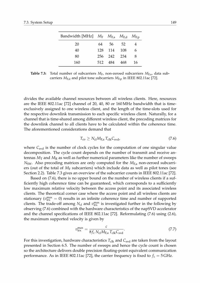
7.3. System Setup 149
Bandwidth [MHz] MF MF,a MF,d MF,p
20 64 56 52 440 128 114 108 680 256 242 234 8160 512 484 468 16
Table 7.3: Total number of subcarriers MF, non-zeroed subcarriers MF,a, data sub-carriers MF,d and pilot tone subcarriers MF,p in IEEE 802.11ac [72].
divides the available channel resources between all wireless clients. Here, resourcesare the IEEE 802.11ac [72] channel of 20, 40, 80 or 160 MHz bandwidth that is time-exclusively assigned to one wireless client, and the length of the time-slots used forthe respective downlink transmission to each specific wireless client. Naturally, for achannel that is time-shared among different wireless client, the precoding matrices forthe downlink channel to all clients have to be calculated within the coherence time.The aforementioned considerations demand that
Tco ≥ NclMF,a TclkCsvd, (7.6)
where Csvd is the number of clock cycles for the computation of one singular valuedecomposition. The cycle count depends on the number of transmit and receive an-tennas MT and MR as well as further numerical parameters like the number of sweepsNSW. Also precoding matrices are only computed for the MF,a non-zeroed subcarri-ers (out of the total of MF subcarriers) which include data as well as pilot tones (seeSection 2.2). Table 7.3 gives an overview of the subcarrier counts in IEEE 802.11ac [72].
Based on (7.6), there is no upper bound on the number of wireless clients if a suf-ficiently high coherence time can be guaranteed, which corresponds to a sufficientlylow maximum relative velocity between the access point and its associated wirelessclients. The theoretical corner case where the access point and all wireless clients arestationary (vmax
trx = 0) results in an infinite coherence time and number of supportedclients. The trade-off among Ncl and vmax
trx is investigated further in the following byobserving (7.6) combined with the hardware characteristics of the napSVD acceleratorand the channel specifications of IEEE 802.11ac [72]. Reformulating (7.6) using (2.6),the maximum supported velocity is given by
vmaxtrx =
c8 fc NclMF,a TclkCsvd
. (7.7)
For this investigation, hardware characteristics Tclk and Csvd are taken from the layoutpresented in Section 6.5. The number of sweeps and hence the cycle count is chosenso the architecture delivers double precision floating-point equivalent communicationperformance. As in IEEE 802.11ac [72], the carrier frequency is fixed to fc = 5 GHz.

150 Chapter 7. System Level Study of a Baseband Transmit System with SVD Precoding
5 10 15 20 25 30 35 40 45 500
5
10
15
Ncl
vmaxtrx
4x46x68x8
Figure 7.1: Maximum supported relative velocity vmaxtrx between access point and
wireless clients for MIMO precoding with the napSVD architecture de-pending on the number of clients Ncl. Transmission setups: 4× 4, 6× 6,and 8× 8 MIMO operating in 160 MHz mode of IEEE 802.11ac [72].
Figure 7.1 shows the maximum mobility that can be supported by a single napSVDentity for a 160 MHz channel as a function of the connected wireless clients. The hor-izontal line at 5 m/s or 18 km/h is a realistic upper bound for the maximum velocitythat occurs in an indoor wireless LAN scenario. The corresponding coherence time is1.5 ms for a 5 GHz carrier frequency. In accordance with the public deployment sce-nario defined in Section 7.2, up to 50 wireless clients are considered, which is a goodupper bound for crowded rooms served by a single access point. For 4× 4 precoding,the maximum velocity remains above the aforementioned upper limit for up to 48clients, so a single napSVD instance can support high mobility for a high number ofclients, even in a crowded public indoor scenario. For 6× 6 and 8× 8 precoding, 5 m/smobility is supported for up to 12 and five clients, respectively, which is sufficient fora domestic scenario. Also, it must be kept in mind that this investigation considersthe pessimistic corner case where all wireless clients are moving at maximum velocityand use the maximum antenna configuration. Therefore, more wireless clients can besupported in a more realistic scenario.
7.3.2 Energy Breakdown
The energy efficiency of the baseband transmit system and the energy distributionamong the FFT, SVD and equalizer units can be estimated based on Table 7.2. Thisstep is essential to assess the impact and the significance of the napSVD architec-ture in a system context. For a first approximation, energy consumption is studiedfor retransmission-free communication, meaning the receiver can correctly decodeeach message at its first transmission attempt. This is a reasonable assumption for
7.3. System Setup 151
transmission scenarios where the SNR is sufficiently high so the FER is low enoughfor retransmissions to have no significant impact on the overall energy consumption.Since common internet applications (e.g., streaming of multimedia content) are muchmore data intensive on the downlink than on the uplink, all following investigationsassume the corner case that the system operates in downlink mode at all times andthat additional overheads like inter-frame space (IFS) and random backoff periods, usedto implement collision avoidance (CA) [90], are negligible.
Let EEQv denote the energy per matrix-vector multiplication of the equalizer listed
in Table 7.2. Based on BDS information bits per data slot, the resulting energy effi-ciency is
ηEQE =
BDS
EEQv MF,a
. (7.8)
The energy per data slot in (7.8) is calculated based on all MF,a non-zeroed subcar-riers that have to be precoded for an OFDM transmission, while the actual payloadresides within MF,d subcarriers, only. With energy EFFT
sym per OFDM symbol, the energyefficiency of the FFT block becomes
ηFFTE =
BDS
EFFTsymMT
. (7.9)
The calculation of the energy efficiency of the SVD block requires further systemlevel parameters. For the corner case of a perfectly static channel, it is sufficient tocalculate the precoding matrices once and use them for all remaining transmissions.In consequence, the energy efficiency of the SVD block converges to infinity. For themore realistic case with a non-zero relative transmitter-receiver velocity, the channelcan only be considered constant for the duration of the coherence time Tco (see (2.6)).In this scenario, the precoding matrices have to be updated after the passing of Tco.Assuming the channel is populated by Ncl wireless clients, a single client receives
NcoDS =
Tco
TOFDMNcl(7.10)
data slots within the coherence time of the channel. Therefore, the energy efficiencyof the SVD block is given by
ηSVDE =
BDSNcoDS
NSWESVDsc MF,a
=BDSTco
NSWESVDsc MF,aTOFDMNcl
, (7.11)
with energy consumption ESVDsc per SVD sweep and subcarrier according to Table 7.2.
The overall energy efficiency of a transmit baseband system consisting of OFDM mod-ulator, SVD and equalizer is
ηBBE =
1
1/ηFFTE + 1/ηSVD
E + 1/ηEQE
. (7.12)

152 Chapter 7. System Level Study of a Baseband Transmit System with SVD Precoding
2x2 4x4 6x6 8x80
50
100
150
4.1 11.624.7
4.9
29.7 29.7 29.7 29.7
Antenna setup
1/η
BB E[p
J/bi
t]
iFFTEQ
SVD
(a) vmaxtrx = 1 m/s
2x2 4x4 6x6 8x8
12.334.7
74.1
4.9
29.7 29.7 29.7 29.7
Antenna setup
(b) vmaxtrx = 3 m/s
2x2 4x4 6x6 8x8
20.5
57.8
123.5
4.9
29.7 29.7 29.7 29.7
Antenna setup
(c) vmaxtrx = 5 m/s
Figure 7.2: Energy distribution among iFFT, SVD computation, and equalization fordomestic scenario. Bandwidth: 20 MHz. Full utilization of spatial di-versity (MT=MS=MR). Modulation: 256-QAM. Frame size: 2,304 byte(uncoded). Channel coding rate: 5/6. Wireless clients: 5.
The calculation of the efficiencies in (7.8), (7.9), (7.11) considers the processing of dataslots but discards the preamble slots (see Section 2.2.1). The underlying reason isthat IEEE 802.11ac [72] employs frame aggregation, i.e., a single PSDU can aggre-gate several MPDUs totaling a payload of up to 4,692,480 bytes to minimize protocoloverhead. A detailed discussion of frame aggregation is out of the scope of this work.However, in the light of this mechanism, the share of the block preamble in the overallPHY layer frame (PPDU) can be considered negligible.
Due to the dependency of ηSVDE on velocity vmax
trx and the number of wirelessclients, ηBB
E has to be studied for several meaningful scenarios. The first one consid-ered here is the domestic scenario introduced in Section 7.2 for a typical two personhousehold with five wireless devices. Figure 7.2 shows the energy consumption anddistribution of this scenario for maximum relative transmitter-receiver velocities of 1,3 and 5 m/s. Several observations can be made based on the data from Figure 7.2.First, the polynomial dependency of the computational complexity of SVD on the in-put matrix size [45] is visible by a corresponding dependency of energy consumptionon the channel matrix size. For vmax
trx = 5 m/s and 4× 4 MIMO, for example, FFT andSVD have a similar energy share, but the SVD becomes clearly dominant for 8× 8.Second, the maximum velocity has a significant impact on the energy share of SVD.For vmax
trx = 1 m/s and 8× 8 MIMO, FFT and SVD still have an approximately equalenergy consumption, while for vmax
trx = 5 m/s, the share of SVD is around 4.2 timesbigger. Regardless of the use case, the equalizer unit has a minor impact on the overallenergy consumption.

7.3. System Setup 153
2x2 4x4 6x6 8x80
100
200
300
400
500
600
700
800
39.3111.1
237.2
29.9 29.9 29.9 29.9
Antenna setup
1/η
BB E[p
J/bi
t]
iFFTEQ
SVD
(a) Ncl = 10
2x2 4x4 6x6 8x8
8.878.6
222.1
474.4
29.9 29.9 29.9 29.9
Antenna setup
(b) Ncl = 20
2x2 4x4 6x6 8x8
13.3117.8
333.2
711.6
29.9 29.9 29.9 29.9
Antenna setup
(c) Ncl = 30
Figure 7.3: Energy distribution among iFFT, SVD computation, and equalization forpublic scenario. Bandwidth: 80 MHz. Full utilization of spatial diver-sity (MT=MS=MR). Modulation: 256-QAM. Frame size: 2,304 byte (un-coded). Channel coding rate: 5/6. Maximum velocity: 5 m/s.
For the public scenario, the number of wireless clients is significantly higher.Therefore, the energy distribution is evaluated for 10, 20 and 30 wireless clients. Re-sults are shown in Figure 7.3. The energy consumption of SVD per transmitted bitrises linearly with the number of wireless clients, since with an increasing amount ofclients, each client can send less data within the channel coherence time. For all usecases with a 4× 4 or higher antenna setup, SVD causes the dominant share of energyconsumption, starting with Ncl = 10 and 4× 4 MIMO, where FFT and SVD have com-parable shares, up to Ncl = 30 and 8× 8 MIMO, where the energy share of SVD is 24times higher than for FFT. Overall, the napSVD block is a significant contributor tothe energy consumption of transmit baseband processing for any communication sce-nario that contains high velocities (for indoor standards), high number of antennas,high number of wireless clients, or any combination thereof.
7.3.3 Area Breakdown
The silicon area requirements of a real-time capable transmit system vary, dependingon the maximum use case supported for the downlink to an individual wireless client(i.e., maximum antenna setup, number of SVD sweeps) and the wireless client sce-nario (i.e., number of wireless clients, maximum velocity). Since silicon area is a major
154 Chapter 7. System Level Study of a Baseband Transmit System with SVD Precoding
production cost factor of the transmitter, it has to be estimated upfront to determinethe feasibility of certain downlink characteristics and deployment scenarios for a spe-cific product type. In this section, silicon area is estimated based on the normalizedarea efficiencies ηEQ
A,n, ηFFTA,n and ηSVD
A,n of the equalizer, the FFT unit, and the SVD unit,respectively, reported in Table 7.2.
The equalizer block multiplies the precoding matrix of each non-zeroed subcarrierby the corresponding set of initial transmit vectors. This results in MF,a matrix-vectormultiplications per OFDM slot. Therefore, the equalizer requires a silicon area of
AEQ =MF,a
ηEQA,nTOFDM
. (7.13)
OFDM modulation has to be executed for each transmit antenna within a time budgetof one OFDM slot. The resulting silicon area is
AFFT =MT
ηFFTA,n TOFDM
. (7.14)
The SVD of each subcarrier has to be renewed within the coherence time of the wire-less channel for each wireless client, which demands a silicon area of
ASVD =MF,aNclNSW
ηSVDA,n Tco
. (7.15)
Since coherence time Tco is proportional to the reciprocal of the relative velocity vtrxbetween transmitter and receiver, ASVD scales linearly with vtrx as well as with thenumber of wireless clients. Silicon areas AEQ and AFFT, on the other hand, do notdepend on the number or relative velocity of wireless clients. The area requirementsfor 90 nm CMOS according to (7.13), (7.14), (7.15) are shown in Table 7.4 and 7.5 fora domestic scenario (i.e., Ncl = 5, vtrx = 5 m/s, WB = 20 MHz) and a public scenario(i.e., Ncl = 50, vtrx = 5 m/s, WB = 80 MHz) respectively. Values are given dependingon the maximum number of SVD sweeps and the number of transmit antennas.
With an area of 0.381 mm2 for the most demanding domestic use case, the transmitbaseband system occupies only one quarter of the area of an equalizer-based MMSE4× 4 MIMO detector [103] performing two detector-decoder iterations for a 20 MHzIEEE 802.11n [69] channel. Therefore, the area requirements shown in Table 7.4 canbe considered feasible for domestic consumer products. Using the maximum con-stellation density and code rate (i.e., 256-QAM, R = 5/6) of IEEE 802.11ac [72], thetransmit system delivers an accumulated peak downlink data rate of 693 Mbit/s cor-responding to 139 Mbit/s per wireless client. The total area is split among equalizer,FFT unit, and SVD unit in shares of 5.7, 42.8, and 51.5 % respectively.
Due to the higher bandwidth and number of wireless clients for the most demand-ing public use case defined in Section 7.2, the resulting silicon area requirement of9.37 mm2 is around 25 times higher than for the domestic scenario. For comparison,an ARM Cortex-A8 processor (excluding L2 cache and NEON extension) occupies

7.4. Design Space 155
NSW
MT 2 4 6 8
1 0.0424 0.0929 0.155 0.2342 0.100 0.177 0.2833 0.199 0.3324 0.381
Table 7.4: Silicon area [mm2] requirements of baseband transmit system for domes-tic scenario. Bandwidth: 20 MHz. Maximum velocity: 5 m/s. Wirelessclients: 5. All components scaled to 90 nm CMOS with 1 V supply volt-age.
NSW
MT 2 4 6 8
1 0.233 0.732 1.60 3.022 1.04 2.55 5.143 3.50 7.254 9.37
Table 7.5: Silicon area [mm2] requirements of baseband transmit system for pub-lic scenario. Bandwidth: 80 MHz. Maximum velocity: 5 m/s. Wirelessclients: 50. All components scaled to 90 nm CMOS with 1 V supply volt-age.
around 4 mm2 of silicon area in 65 nm CMOS [6], or 7.67 mm2 when scaled to 90 nmCMOS. In conclusion, the area requirements for the public use case can be consid-ered too high for consumer products for domestic use, but suitable for more powerfulprofessional solutions deployed in a public scenario. For the maximum constella-tion and code rate of IEEE 802.11ac [72], the accumulated peak downlink data rate is3.12 Gbit/s or 62.4 Mbit/s per wireless client. The area distribution among equalizer,FFT unit, and SVD unit is 1.0, 8.6, and 90.4 % respectively.
7.4 Design Space
In a wide design space that spans across different antenna setups, number of eigen-modes, constellation alphabets, code rates, and numerical parameters, it is beneficialto conduct some up-front evaluations based on a reduced parameter set. This en-ables an isolated analysis and visualization of the effects that are going to play animportant role in the following exhaustive design space exploration in Section 7.6.

156 Chapter 7. System Level Study of a Baseband Transmit System with SVD Precoding
14 16 18 20 22 24 26 28 30 32 34 36 38 40 420
5
10
15
20
25
2.5 dB
1.2 dB
0.5 dB
SNR
ηS
[bit
/s/H
z]MS=2, NSW=1 MS=2, NSW=2MS=3, NSW=1 MS=3, NSW=2MS=4, NSW=1 MS=4, NSW=2
Figure 7.4: Spectral efficiency for MT=MR = 4, MS ∈ {2, 3, 4}. Modulation: 256-QAM. Frame size: 2,304 byte (uncoded). Channel coding: LDPC, code-word length 1944 bit, code rate: 5/6. Channel model: slow fading.
Therefore, Section 7.4.1 presents spectral efficiencies for different numbers of eigen-modes for a fixed antenna setup, constellation alphabet, and code rate. Next, Section7.4.2 discusses the impact of the antenna setup on spectral efficiency. Code rate andconstellation alphabet remain constant, but the number of eigenmodes is chosen tomaximize spectral efficiency. Finally, Section 7.4.3 shows the impact of AMC, whereconstellation alphabet and code rate may vary, for a fixed antenna setup.
7.4.1 Eigenmode Selection
The transceiver system described in Section 7.3 has the option to choose the numberof eigenmodes MS according to the channel state and the optimization target. Uti-lizing more eigenmodes delivers a higher data rate Θ and spectral efficiency ηS butat the same time, it demands a higher SNR to be operational. This trade-off is il-lustrated in Figure 7.4 which shows spectral efficiency ηS as a function of the SNRfor 4× 4 MIMO and different number of eigenmodes. The constellation alphabet isfixed to 256-QAM and the code rate is set to 5/6. The number of SVD sweeps NSWis varied between one and two to show the impact of the numerical parameter oncommunication performance.
Figure 7.4 shows the feasibility of different MS depending on the SNR, whereMS = 3 outperforms MS = 2 for SNRs beyond 25 dB and MS = 4 becomes feasiblefor an SNR equal or above 34 dB. From an energy efficiency perspective, it is desir-able to switch to a higher number of eigenmodes as soon as it becomes feasible, sincethe energy consumption per SVD depends on MT and MR but not on MS. Hence,increasing MS means that the same amount of energy per SVD is used to transmitmore data. Figure 7.4 also illustrates the trade-off among data rate and energy effi-

7.4. Design Space 157
5 10 15 20 25 30 35 40 450
10
20
30
40
50
MS=1
MS=2
MS=3
MS=4
MS=5
MS=6
MS=7
MS=80.7 dB
2.5 dB
2.5 dB
SNR
ηS
[bit
/s/H
z]
4x4, NSW=14x4, NSW=26x6, NSW=16x6, NSW=26x6, NSW=38x8, NSW=18x8, NSW=28x8, NSW=38x8, NSW=4
Figure 7.5: Maximum spectral efficiency per antenna and SVD sweep setup forMT=MR ∈ {4, 6, 8}, MS ≤ MT. Modulation: 256-QAM. Frame size:2,304 byte (uncoded). Channel coding: LDPC, codeword length 1944 bit,code rate: 5/6. Channel model: slow fading.
ciency when varying numerical parameters (i.e., NSW). SVD computation for NSW = 2consumes twice as much energy as NSW = 1 but offers a gain in terms of SNR. Thatgain depends on the SNR and the position on the curve’s trajectory, though. This isvisualized in Figure 7.4 by the gap between the trajectories for NSW = 1 and NSW = 2for all MS at the position where 95 % of the theoretical maximum spectral efficiencyis reached. At 2.5 dB, the gap is most significant for the highest MS = 4 and dimin-ishes down to 0.5 dB for MS = 2. However, when the SNR exceeds a certain value,the FERs for NSW = 1 and NSW = 2 have both dropped so far that the resultingspectral efficiencies are hardly distinguishable. For these SNRs, the SVD computationenergy can be reduced by 50 % by switching to NSW = 1 without any notable effecton communication performance.
7.4.2 Antenna Setup
In Section 2.3.2, it was shown that for a fixed number of eigenmodes/streams MS,transmission setups with higher number of antennas at the transmit and receive sideachieve any target FER at a lower SNR than setups with less transmit and receiveantennas, given that the same modulation and coding scheme is used. The advantagein FER translates to a superior data rate Θ and spectral efficiency ηS according to (7.3)

158 Chapter 7. System Level Study of a Baseband Transmit System with SVD Precoding
−5 0 5 10 15 20 25 30 35 400
5
10
15
20
25
1.6 dB
9.2 dB
14.7 dB
SNR
ηS
[bit
/s/H
z]4-QAM16-QAM64-QAM256-QAM
Figure 7.6: Adaptive modulation and coding for 4 × 4 MIMO using NSW=2 SVDsweeps and MS ∈ {2, 3, 4} spatial streams. Frame size: 2,304 byte (un-coded). Channel coding: LDPC, codeword length 1944 bit. Channelmodel: slow fading.
and (7.4). Figure 7.5 shows the spectral efficiency for antenna setups MT = MR ∈{4, 6, 8} using a 256-QAM constellation alphabet and code rate R = 5/6. Comparedto Figure 7.4, Figure 7.5 shows the envelope of ηS per antenna setup for all numbersof streams. The trajectories are plotted for multiple choices of NSW to illustrate theimpact of numerical parameters on communication performance, where the curve fora certain number of sweeps is only shown if it is visibly different from the curvesgenerated for less sweeps.
Figure 7.5 illustrates the superior spectral efficiency provided by a transceiversetup with more transmit and receive antennas, and the advantage increases forhigher MS. For MS = 2, for example, the SNR offset between the points where ηSconverges to its theoretical maximum for MT = MR = 4 and MT = MR = 8 is around10 dB. For MS = 4, the corresponding offset has increased to approximately 20 dB.Another interesting aspect is the impact of NSW on ηS for 6× 6 and 8× 8 MIMO. Par-ticularly for the latter, the spectral efficiency advantage of NSW = 4 over NSW = 3 issmall. The SNR gap at 95 % of the theoretical maximum spectral efficiency is shownin Figure 7.5 for the highest and second highest number of sweeps. For 8× 8 MIMO,this gap is limited to 0.7 dB for NS = 8 and and disappears completely for NS ≤ 7.Therefore, from an energy efficiency perspective, restraining NSW ≤ 3 is an attractiveoption.
7.4.3 Adaptive Modulation and Coding
The investigations in Section 7.4.1 and 7.4.2 have been conducted for a fixed con-stellation alphabet and code rate. However, the IEEE 802.11ac standard [72] defines

7.5. Methodology 159
multiple modulation and coding schemes (MCSs) covering 4, 16, 64, and 256-QAM andcode rates R ∈ {1/2, 2/3, 3/4, 5/6}. A system that employs AMC is able to switchamong different MCSs to pursue a specific optimization target. To illustrate the vastamount of resulting use cases, Figure 7.6 shows spectral efficiency ηS for all previ-ously mentioned MCSs and MS ∈ {2, 3, 4} for a 4× 4 antenna setup. The number ofsweeps is fixed to the maximum numerical requirement NSW = 2 in order not to over-populate the plot. Additionally, the envelope with the maximum spectral efficiency ishighlighted per constellation in bold lining.
Compared to Figure 7.4, the addition of AMC creates a smoothly increasing spec-tral efficiency envelop that spans a wider SNR range. Generally, less dense constel-lations are feasible at lower SNRs but their slope of ηS over SNR is also lower sothat even when operating at high code rates, they are quickly outperformed by moredense constellations operating at lower code rates. It is interesting to observe thatthese transitions already happen at comparably low SNRs. At 1.6 dB, 4-QAM is su-perseded by 16-QAM which is utilized up to 9.2 dB. Thereafter, 64-QAM providessuperior spectral efficiency up to 14.7 dB, followed by 256-QAM.
7.5 Methodology
This section elaborates on the methodology that is used in Section 7.6 to explore thedesign space described in Section 7.4 and to perform optimizations of different targetfunctions composed of the performance metrics defined in Section 7.1. All requiredalgorithmic performance metrics (i.e., throughput Θ, spectral efficiency ηS, number oftransmit attempts Ntx) are calculated based on FERs derived for all considered AMCconfigurations, antenna setups, number of streams MS, and number of SVD sweepsNSW by extensive Monte-Carlo simulations. A small share of these FERs were alreadypresented in Section 6.4 to show the numerical precision requirements of precodingusing the napSVD architecture. Hardware-related performance numbers (i.e, energyefficiency ηE, power consumption P) combine the FERs or derived metrics with hard-ware benchmarks taken from the napSVD accelerator presented in Chapter 6, thededicated matrix-vector multiplication units for equalizing presented in this chapter,or from implementations in the open literature (compare Table 7.2).
Due to the wide design space that has to be explored in this chapter, a flexibledesign space exploration and performance metric evaluation software was developedin this work, using the Python programming language [93]. The object-oriented soft-ware consists of two main components: the use case evaluation class and the use caseiterator. The use case evaluation class represents one particular use case defined byantenna setup (i.e., MT, MR), number of eigenmodes/streams MS, code rate R, con-stellation alphabet, and numerical parameters (i.e., NSW). At its instantiation, a usecase evaluation class reads in its respective FER-trajectory and the relevant hardwarecharacteristics. The class interface provides a set of methods that compute all relevantperformance metrics based on this data for a given set of environmental parameters(i.e., velocity vtrx, number of wireless clients Ncl, SNR). The use case iterator starts

160 Chapter 7. System Level Study of a Baseband Transmit System with SVD Precoding
out by creating a set of instances of the use case evaluation class based on a freelyconfigurable design space specification. This is of particular importance for optimiza-tions carried out on a partitioned design space (e.g., Figure 7.7). Next, the use caseiterator steps through the coordinates in the space defined by the environmental pa-rameters. For each of these coordinates, the iterator performs an exhaustive searchbased optimization.
The optimization process follows the basic idea presented in [14] transferred toa baseband transmit system. The three central steps to optimize a primary target,potentially constrained by a set of secondary targets, are summarized in the following.
• Feasible set generation selects the subset of the design space that fulfills theconstraints imposed by the secondary optimization target for the current envi-ronmental parameters. When optimizing spectral efficiency, for example, onemight impose an additional constraint on energy efficiency. The use cases thatfulfill the energy efficiency constraint form the feasible set. If no secondaryoptimization target is specified, the feasible set contains the entire design space.
• Candidate set generation conducts an exhaustive search in the feasible set andselects the best use case according to the primary optimization target. If nosecondary optimization target is specified, the optimization is finished at thispoint. Otherwise, a candidate set is selected as a subset of the feasible set,where all use cases in the candidate set deliver performance metrics for theprimary optimization target that deviate only by a small margin from the bestuse case. Within this chapter, that margin is set to 2 % of the optimal value.Similar to the receiver study conducted in [14], it was noted in this work that forthe transmit system described in Section 7.3, often, use cases exist that performalmost as good as the best candidate with respect to the primary optimizationtarget, but are significantly superior with respect to the secondary optimizationtarget. At the plateaus of spectral efficiency shown in Figure 7.4 for 4× 4 MIMO,for example, the spectral efficiencies for one and two SVD sweeps are hardlydistinguishable, while the former consumes only half of the energy of the latterfor SVD calculation.
• Candidate selection choses the most desirable candidate from the candidate set.While the selection method generally is configurable, in this chapter, the use casethat performs best with respect to the secondary optimization target is selected.
7.6 Multidimensional Design Space Exploration
This section explores the design space laid out in Section 7.4 by optimizing and con-straining different performance metrics using the optimization flow introduced inSection 7.5. Section 7.6.1 optimizes spectral efficiency while constraining energy ef-ficiency or power consumption and vice versa. The optimizations are performed forthe domestic and the public deployment scenario introduced in Section 7.2. Section7.6.2 imposes an additional latency constraint for the energy efficiency and spectral

7.6. Multidimensional Design Space Exploration 161
efficiency optimization in the domestic scenario and discusses the impact on the op-timization results.
7.6.1 Spectral Efficiency, Energy Efficiency & Power Consumption
As pointed out in Section 7.1, spectral efficiency ηS and energy efficiency ηE are twomajor performance indicators of a wireless communication system. In addition, theyare often oppositional, since spectral efficiency comes at the expense of higher com-putational complexity and therefore higher energy consumption. However, both areworthwhile from a communication system perspective. A system with high spectralefficiency delivers high data rates to as many wireless clients as possible within theconfines of the available bandwidth. High energy efficiency corresponds to deliver-ing high amounts of information per unit of energy, or equivalently, high throughputper unit of power, which is important to enable eco-friendly communication systems.For a system with a highly variable computational load, it may be more desirable toconstrain or minimize power consumption to ensure the integrity of the processingsystem. It must be kept in mind that this is fundamentally different from a maxi-mization or constraint of energy efficiency, where an increased number of wirelessclients would result in an additional computational load and hence a potentially crit-ical power consumption. For this reason, Section 7.6.1.1 that studies the domesticscenario with a fixed number of wireless clients investigates spectral efficiency andenergy efficiency, while Section 7.6.1.2 focuses on spectral efficiency and power con-sumption for the public scenario with a variable number of wireless clients.
7.6.1.1 Domestic Scenario
To generate an overview of the achievable efficiencies, Figure 7.7 shows an optimiza-tion of spectral efficiency and energy efficiency, performed separately for antennasetups MT = MR ∈ {4, 6, 8}. The optimization for both targets is performed withoutsecondary constraints, so Figure 7.7 shows the maximum achievable performance forboth targets. As expected, 8× 8 MIMO provides the highest spectral efficiency, while4 × 4 MIMO achieves the best overall energy efficiency. Comparing the optimiza-tions for ηS and ηE, the achieved spectral efficiencies vary less than the correspondingenergy efficiencies, confirming earlier assessments that a small decrease in spectralefficiency often offers a significant gain in energy efficiency. Another interesting ob-servation can be made comparing the energy efficiencies of different antenna setupsfor a fixed SNR. Section 6.5.1 stated that for a floating-point equivalent SVD computedby the napSVD architecture, the energy consumption of the 8× 8 variant is around 12times higher than for the 4× 4 version. In comparison, the energy efficiency achievedwith energy efficiency as primary optimization target is only around 1.6 times higherfor 4× 4 than for 8× 8, before the curve for the latter plateaus around 35 dB. Sev-eral factors contribute to this discrepancy. First, an 8× 8 transmission system has atwo times higher maximum data rate Θmax than an otherwise identical 4× 4 system.Second, the aforementioned floating-point equivalent SVD uses two and four SVD

162 Chapter 7. System Level Study of a Baseband Transmit System with SVD Precoding
−5 0 5 10 15 20 25 30 35 400
10
20
30
40
50η
S[b
it/s
/Hz]
4x4, ηS optimized4x4, ηE optimized6x6, ηS optimized6x6, ηE optimized8x8, ηS optimized8x8, ηE optimized
(a) Spectral efficiency
−5 0 5 10 15 20 25 30 35 400
5
10
15
20
25
SNR
ηE
[bit
/nJ]
(b) Energy efficiency
Figure 7.7: Maximizing spectral efficiency and energy efficiency for domestic sce-nario and individual antenna setups: MT=MR ∈ {4, 6, 8}. Bandwidth:20 MHz. Frame size: 2,304 byte (uncoded). Channel coding: LDPC,codeword length 1944 bit. Channel model: slow fading. Wireless clients:5. Maximum velocity: 5 m/s.
sweeps for 4× 4 and 8× 8, respectively, while an otherwise unconstrained system op-timized for energy efficiency will use one sweep for both. Third, the spatial diversitygain (see Section 2.3.2) of the 8× 8 setup renders use cases with more eigenmodesfeasible for lower SNRs than for the 4× 4 antenna configuration. These effects com-bined put the aforementioned difference for floating-point equivalent computationinto perspective and show that the costs of using higher antenna setups are less thantypically estimated, particularly for processing systems that employ NAP.

7.6. Multidimensional Design Space Exploration 163
Figure 7.8 shows the results of an optimization with spectral efficiency as primaryoptimization target, imposing different constraints on energy efficiency. In this opti-mization, the design space encompasses all antenna setups. The number of transmitantennas chosen by the optimization procedure described in Section 7.5 is shown inFigure 7.8c along with the number of SVD sweeps in Figure 7.8d. Figure 7.7 showedthat at any SNR, the antenna setup with most transmit and receive antennas achievesthe highest spectral efficiency due to the corresponding spatial diversity gain (see Sec-tion 2.3.2). However, higher antenna setups also have a higher energy consumption,so they only become feasible if the SNR is sufficient to enable operation at an MCSwith high code rate and dense constellation alphabet (see Section 7.4.3). Therefore, anenergy efficiency constrained spectral efficiency optimization starts from the lowestantenna setup at low SNR and switches to the next higher antenna setup as soon asthe SNR is sufficiently high so that a use case fulfilling the energy efficiency constraintbecomes feasible. For stricter (i.e., higher) constraints on ηE, a higher SNR is required.Figure 7.8c illustrates this relationship. For a mild constraint of ηE ≥ 5 bit/nJ, 8× 8MIMO becomes feasible at 13 dB. For a medium constraint (i.e., ηE ≥ 10 bit/nJ), itbecomes feasible for an SNR greater or equal 26 dB, whilst only permitting one SVDsweep. Finally, for a strict constraint of ηE ≥ 15 bit/nJ, transmission with eight anten-nas is not feasible at all for the observed SNR range.
Figure 7.9 presents an optimization with energy efficiency as primary optimiza-tion target and spectral efficiency as secondary target. When optimizing energy effi-ciency, the transmitter switches to use cases using as little transmit antennas as possi-ble as soon as the SNR is high enough for these use cases to become feasible. The pointwhere the switch happens depends on the constraint imposed on spectral efficiency.A low constraint on ηS can be fulfilled by an MCS with low code rate and sparseconstellation alphabet which becomes feasible for low SNR, while a stricter constraintcan only be satisfied by an MCS with high code rate and dense constellation alphabetwhich requires a higher SNR (compare Figure 7.6). This effect is visible in Figure7.9c. For a low constraint of ηS ≥ 8 bit/s/Hz, the transmitter switches from 8× 8 to6× 6 MIMO at 11 dB and to 4× 4 at 15 dB. A medium constraint of ηS ≥ 20 bit/s/Hzcan be fulfilled by 6 × 6 MIMO upwards from an SNR of 25 dB, and 4 × 4 MIMObecomes feasible at 37 dB. Finally, a strict constraint of ηS ≥ 32 bit/s/Hz cannot bemet by any 4× 4 or 6× 6 MIMO transmission mode using the available MCSs of IEEE802.11ac [72], regardless of the SNR. Therefore, the constraint of ηS ≥ 32 bit/s/Hzrequires an 8× 8 MIMO setup for the entirety of the observed SNR range. Similar ob-servations as for the number of antennas can be made for the number of SVD sweepsshown in Figure 7.8d. In order to optimize energy efficiency, the transmitter reducesthe number of sweeps as soon as the SNR is high enough so the spectral efficiencyconstraint can be fulfilled despite the reduced communication performance.
Overall, the constrained optimizations for spectral efficiency and energy efficiencyin Figure 7.8 and 7.9 lead to very different optimization strategies and results, partic-ularly for a communication system including the napSVD architecture, offering highflexibility with respect to supported use cases and numerical precision settings. Theresults clearly show the advantages of a versatile precoding system and its adaptabil-

164 Chapter 7. System Level Study of a Baseband Transmit System with SVD Precoding
ity to different operational constraints. At the same time, they underline the impor-tance of a clear definition of optimization targets and constraints to deliver the desiredend user experience.
7.6.1.2 Public Scenario
Two major distinguishing factors between the public and the domestic scenario are thenumber of wireless clients and their behavior. A communication system for a publicscenario has to be prepared for a higher number of wireless clients, and the numberof wireless clients in the public scenario is subject to a higher variance (e.g., due totime-dependent customer behavior). For this reason, the optimization performed forthe domestic scenario has to be adapted to account for these differences. Accordingto (7.4) and (7.5), the power consumption of the baseband transmit system is given by
P =WB,dηS
ηE. (7.16)
For a fixed bandwidth WB,d, P solely depends on the quotient of ηS and ηE. The formeris only linked to the SNR via the corresponding FER (see (7.3), (7.4)). Energy efficiencyηE, on the other hand, also depends on the number of wireless clients (see (7.11)) inaddition to the SNR. In consequence, the number of clients influences the power con-sumption. Power consumption in combination with the external temperature and thecooling system may become critical with respect to heat dissipation, which in turnmay compromise the device integrity. This is of particular importance for highly in-tegrated devices with many components on one chip due to dark silicon effects (seeSection 1.3), predicting that for shrinking CMOS feature sizes, decreasing fractionsof a chip can run at full utilization due to thermal constraints. In response, it is ofutmost importance that a processing system offers parameters to lower power con-sumption while the system performance degrades gracefully. In case of the basebandtransmit system discussed in this chapter, the number of transmit antennas and SVDsweeps can be adapted to reduce the computational load, which allows for a lowerclock frequency and hence a lower power consumption. These mechanisms are inves-tigated further in Figure 7.10 which maximizes spectral efficiency while constrainingthe power consumption of the transmit baseband processing system to 500 mW for avarying number of wireless clients. Throughout this investigation, it is assumed thatthe clock frequency can be scaled continuously.
Figure 7.10a shows the impact of the power constraint on the achieved spectralefficiency for Ncl ∈ {10, 30, 50} wireless clients. For Ncl = 10, the power constrainthas little effect on spectral efficiency. As illustrated in Figure 7.10c, the optimizationprocess chooses an eight antenna transmission for the entire observed SNR range.Below 35 dB, the curve is close to identical to the results of the unconstrained spectralefficiency optimization for 8× 8 MIMO indicated by the dotted line. For Ncl = 30,transmission is limited to 6× 6 MIMO and one sweep, and transmission for Ncl = 50is only feasible for 4× 4 MIMO. The power consumption traces in Figure 7.10b eachshow a significant variance. Major changes in power consumption occur whenever

7.6. Multidimensional Design Space Exploration 165
−5 0 5 10 15 20 25 30 35 400
10
20
30
40
50η
S[b
it/s
/Hz]
ηE ≥ 5 bit/nJηE ≥ 10 bit/nJηE ≥ 15 bit/nJ
(a) Spectral efficiency
−5 0 5 10 15 20 25 30 35 400
5
10
15
20
25
ηE
[bit
/nJ]
(b) Energy efficiency
−5 0 5 10 15 20 25 30 35 404
6
8
MT
(c) Transmit antennas
−5 0 5 10 15 20 25 30 35 401
234
SNR
NSW
(d) SVD sweeps
Figure 7.8: Maximizing spectral efficiency, constraining energy efficiency for domes-tic scenario. Bandwidth: 20 MHz. Frame size: 2,304 byte (uncoded).Channel coding: LDPC, codeword length 1944 bit. Channel model: slowfading. Wireless clients: 5. Maximum velocity: 5 m/s.

166 Chapter 7. System Level Study of a Baseband Transmit System with SVD Precoding
−5 0 5 10 15 20 25 30 35 400
10
20
30
40
50η
S[b
it/s
/Hz]
ηS ≥ 8 bit/s/HzηS ≥ 20 bit/s/HzηS ≥ 32 bit/s/Hz
(a) Spectral efficiency
−5 0 5 10 15 20 25 30 35 400
5
10
15
20
25
ηE
[bit
/nJ]
(b) Energy efficiency
−5 0 5 10 15 20 25 30 35 404
6
8
MT
(c) Transmit antennas
−5 0 5 10 15 20 25 30 35 401
234
SNR
NSW
(d) SVD sweeps
Figure 7.9: Maximizing energy efficiency, constraining spectral efficiency for domes-tic scenario. Bandwidth: 20 MHz. Frame size: 2,304 byte (uncoded).Channel coding: LDPC, codeword length 1944 bit. Channel model: slowfading. Wireless clients: 5. Maximum velocity: 5 m/s.

7.6. Multidimensional Design Space Exploration 167
−5 0 5 10 15 20 25 30 35 400
10
20
30
40
50η
S[b
it/s
/Hz]
Ncl = 10Ncl = 30Ncl = 50Ncl = 10, unconstr.
(a) Spectral efficiency
−5 0 5 10 15 20 25 30 35 40200
300
400
500
P[m
W]
(b) Power
−5 0 5 10 15 20 25 30 35 404
6
8
MT
(c) Transmit antennas
−5 0 5 10 15 20 25 30 35 401
234
SNR
NSW
(d) SVD sweeps
Figure 7.10: Maximizing spectral efficiency, constraining power consumption to500 mW for public scenario. Bandwidth: 80 MHz. Frame size: 2,304byte (uncoded). Channel coding: LDPC, codeword length 1944 bit.Channel model: slow fading. Maximum velocity: 5 m/s.

168 Chapter 7. System Level Study of a Baseband Transmit System with SVD Precoding
−5 0 5 10 15 20 25 30 35 400
10
20
30
40
50η
S[b
it/s
/Hz]
Ncl = 10, ηS ≥ 7 bit/s/HzNcl = 30, ηS ≥ 21 bit/s/HzNcl = 50, ηS ≥ 35 bit/s/Hz
(a) Spectral efficiency
−5 0 5 10 15 20 25 30 35 400
1
2
3
P[W
]
(b) Power
−5 0 5 10 15 20 25 30 35 404
6
8
MT
(c) Transmit antennas
−5 0 5 10 15 20 25 30 35 401
234
SNR
NSW
(d) SVD sweeps
Figure 7.11: Minimizing power consumption, constraining spectral efficiency forpublic scenario. Bandwidth: 80 MHz. Frame size: 2,304 byte (un-coded). Channel coding: LDPC, codeword length 1944 bit. Channelmodel: slow fading. Maximum velocity: 5 m/s.

7.6. Multidimensional Design Space Exploration 169
the use cases for adjacent SNRs employ a different number of SVD sweeps. Thesepoints are significant for power consumption due to the direct proportionality of thenumber of sweeps to computational complexity. Minor variations, on the other hand,are caused by changes of MS. Overall, there is a considerable impact of the powerconstraint on the user experience in terms of data rate for a high number of wirelessclients. Comparing the trajectories of ηS for Ncl = 10 and Ncl = 50 shows that thelatter only achieves around 50 % of the spectral efficiency (measured at 30 dB) of theformer. In addition, the resulting data rate also has to be divided among five timesmore wireless clients.
Figure 7.11 shows the result of an optimization for minimum power consumptionwhile constraining spectral efficiency. Trajectories are given for Ncl ∈ {10, 30, 50}wireless clients. For a public communication system with a highly varying number ofclients, it is desirable that the system can adapt to the number of clients and providea fixed minimum data rate to each of them. For that reason, the system-wide spectralefficiency constraint ηS is scaled up along with the number of wireless clients Ncl.The spectral efficiency per client is set to ηS/Ncl ≥ 0.7 bit/s/Hz. For an 80 MHzIEEE 802.11ac [72] channel with 234 out of 256 subcarriers used for data transmission,the corresponding guaranteed data rate is 51.2 Mbit/s, which is approximately theaverage peak data rate of a fixed internet connection in Germany at the time of thewriting of this thesis [3].
The number of wireless clients with the aforementioned guaranteed data rate perclient has a significant impact on the SNR at which operation becomes feasible. For10, 30 and 50 wireless clients, this point is at an SNR of 3, 18 and 30 dB, respectively.At these points, the power consumption of the baseband processing system reachesits maximum, since at that SNR, the spectral efficiency constraint can only be fulfilledby an 8× 8 antenna setup and a high number of sweeps. As shown in Figure 7.11c,the antenna setup can be reduced to 6× 6 and 4× 4 at 7 and 12 dB for Ncl = 10, andat 24 and 39 dB for Ncl = 30. For 50 wireless clients, the spectral efficiency constraintcan only be fulfilled by an 8× 8 antenna setup for the observed SNR range. However,Figure 7.11d shows that the number of SVD sweeps can be reduced from three at30 dB to one at 33 dB, which enables a significant reduction of power consumption.
7.6.2 Latency
Apart from data rate, latency (i.e., the amount of time from the first transmit at-tempt until successful reception at the receiver) is a central performance indicatorfor a wireless communication system from an end-user perspective. The quantifica-tion of latency depends on the perspective of the analysis (e.g., at which layer of theISO OSI reference model [133] time is measured) and on details of the receiver im-plementation (e.g., [14]). The latter is outside the scope of this analysis. To abstractfrom details of the receiver architecture, this section analyzes the expected numberof transmit attempts Ntx necessary for a frame to be decoded correctly in the com-munication system described in Section 7.3. According to Section 7.1, the expected

170 Chapter 7. System Level Study of a Baseband Transmit System with SVD Precoding
−5 0 5 10 15 20 25 30 35 401
1.02
1.04
1.06
1.08
1.1
1.12
1.14
1.16
1.18
1.2
SNR
Ntx
optimize ηS, Ntx = 1.024optimize ηE, Ntx = 1.048
Figure 7.12: Expected number of transmit attempts per frame for domestic scenario.Bandwidth: 20 MHz. Frame size: 2,304 byte (uncoded). Channel cod-ing: LDPC, codeword length 1944 bit. Channel model: slow fading.
number of transmit attempts per frame for a system with a hybrid ARQ type 1 [28]retransmission scheme is
Ntx =1
1− FER. (7.17)
Figure 7.12 shows Ntx for the aforementioned domestic communication scenario.One trace is optimized for spectral efficiency ηS, the other is optimized for energyefficiency ηE, both without imposing any secondary constraints on the optimization.When optimizing for energy efficiency, the average expected number of transmit at-tempts per frame, Ntx, over the observed SNR range is notably higher than for thespectral efficiency optimization. From an energy perspective, it is often more bene-ficial to switch to a less energy consuming transmission mode and thereby accept aslight increase of retransmissions instead of operating in an almost error free modewith high energy consumption. Spectral efficiency optimization maximizes the quo-tient of the maximum theoretical data rate Θmax and the number of transmit attemptsNtx per frame (see (7.3)) over all potential transceiver setups for each individual SNR.For a given Θmax, the optimization will therefore choose Ntx as small as possible with-out concern for energy consumption. However, there are several potential choices forΘmax at each SNR. In consequence, optimizing ηS is not equivalent to a minimiza-tion of latency. Minimizing latency without any secondary constraints corresponds tochoosing a communication setup with the lowest possible FER. For the given trans-mit system, this is achieved by choosing the highest antenna setup, the lowest coderate, constellation density and number of eigenmodes, and the highest number of

7.6. Multidimensional Design Space Exploration 171
SVD sweeps. Naturally, the outcome of this optimization is neither favorable from anenergy efficiency nor spectral efficiency perspective.
For certain types of applications, latency can have a significant impact on the userexperience. Prominent examples of such applications are voice and video telephony.For these applications, it makes sense to constrain the expected number of transmitattempts as a secondary target function. The primary optimization target functionhas to be chosen to reflect the nature of the application. The required data rate forvoice communication is comparably low in relation to the achievable data rates ofIEEE 802.11 [71] wireless LAN. The ITU-T G.722 [75] audio codec that covers 7 kHzof audible spectrum, for example, requires a data rate of only 64 kbit/s. On a 20 MHzIEEE 802.11ac [72] channel, the corresponding spectral efficiency per wireless clientis less than 0.004 bit/s/Hz. Therefore, the transmission can be optimized for energyefficiency. A video stream encoded by the common H.264 [74] standard using a basicBaseline, Level 3.2 profile, on the other hand, requires a data rate of 20 Mbit/s. Forthe aforementioned channel, this corresponds to a spectral efficiency of 1.23 bit/s/Hzper wireless client. Using the higher quality Baseline, Level 4.2 profile even demands50 Mbit/s of data rate, resulting in a spectral efficiency requirement of 3.08 bit/s/Hz.In conclusion, video telephony demands medium to high data rates for the communi-cation system presented in this chapter (compare Figure 7.7, for example), dependingon the number of wireless clients. Transmission of uncompressed video (e.g., to wire-less displays) imposes even higher demands on data rates while demanding a lowlatency transmission.
Based on these considerations, Figure 7.13 presents the results of an optimizationof the domestic scenario baseband transmit system for spectral efficiency and energyefficiency, respectively. Both optimization are constrained by a strict upper limit ofNtx ≤ 1.001 on the expected number of transmit attempts per frame. Without anyconstraint on energy efficiency, the spectral efficiency optimization selects MT = 8 ex-clusively, since for a fixed number of eigenmodes, fixed coding and fixed modulation,the setup with the highest number of antennas provides the lowest FER and thereforethe highest data rate at any SNR (see Section 2.3.2). This optimization strategy resultsin an overall poor energy efficiency, though. Optimizing energy efficiency withoutany constraint on spectral efficiency shows a fundamentally different behavior. Inorder to save energy, the system switches to the lowest antenna setup (i.e., MT = 4)as soon as FERs have fallen enough to deliver an Ntx below the set threshold.
Figures 7.13a and 7.13b also show the results of unconstrained optimizations ofηS and ηE which are an upper bound to the optimizations constrained by Ntx. Whenoptimizing ηS, the penalty in terms of spectral efficiency for imposing an additionalconstraint on the number of transmit attempts and thus on latency is rather limited.This is particularly noteworthy in the context of Figure 7.12 which shows that thenumber Nrtx = Ntx − 1 of retransmit attempts of the unconstrained optimization,averaged over the observed SNR range, is more than 20 times higher than the limitfor the constrained optimization. However, the rich choice of MCSs that forms adense cluster of FERs and spectral efficiencies along the SNR-axis (see Figure 7.6)enables the system to achieve the target FER by switching to a lower MCS with just

172 Chapter 7. System Level Study of a Baseband Transmit System with SVD Precoding
−5 0 5 10 15 20 25 30 35 400
10
20
30
40
50
ηS
[bit
/s/H
z]
optimize ηS, Ntx ≤ 1.001optimize ηSoptimize ηE, Ntx ≤ 1.001optimize ηE
(a) Spectral efficiency
−5 0 5 10 15 20 25 30 35 400
5
10
15
20
25
ηE
[bit
/nJ]
(b) Energy efficiency
−5 0 5 10 15 20 25 30 35 404
6
8
SNR
MT
(c) Transmit antennas
Figure 7.13: Maximizing energy efficiency and spectral efficiency, constraining ex-pected transmit attempts per frame for domestic scenario. Bandwidth:20 MHz. Frame size: 2,304 byte (uncoded). Channel coding: LDPC,codeword length 1944 bit. Channel model: slow fading.

7.7. Discussion 173
a marginal impact on spectral efficiency. The retransmission constraint has a moresignificant impact on the energy efficiency optimization, and the gap of ηE betweenthe constrained and unconstrained optimization widens for smaller choices of Ntx.This is due to the fact that FER cannot be traded for energy consumption because ofthe constraint imposed on the FER via Ntx.
7.7 Discussion
This chapter embedded the napSVD architecture into a baseband transmit systemcomposed of an OFDM modulator taken from the open literature [131], a precodingpreprocessor (i.e., the napSVD) to calculate the precoding matrices, and an equalizerto multiply the precoding matrices by the initial transmit vectors. A domestic anda public deployment scenario for an IEEE 802.11ac [72] based wireless LAN weredefined, the former mimicking an urban home with five wireless clients sharing a20 MHz channel, the latter representing a public place (e.g., hotel lobby, coffee shop)with a varying number of up to 50 wireless clients sharing an 80 MHz channel. Sili-con area was estimated so that the communication system is real-time capable up to8× 8 MIMO using all eight eigenmodes (MS = 8) with double precision floating-pointequivalent algorithmic performance. These requirements translate to an area require-ment of only 0.381 mm2 for the domestic scenario and 9.37 mm2 for the public scenariousing a 90 nm CMOS technology with 1 V supply voltage. For a retransmission-freecommunication link, which is a valid approximation in the low FER regime, the en-ergy efficiency of a transmission with MT = MR = MS = 8 for the maximum modu-lation and coding setup in IEEE 802.11ac [72] is 6.32 bit/nJ for the domestic scenarioand 0.819 bit/nJ for the public scenario. The resulting peak power consumptions are110 mW and 3.81 W, respectively.
A core aspect of the napSVD architecture is versatility with respect to supportedcommunication setups (i.e., antenna setup, number of eigenmodes, number of SVDsweeps). Combined with the modulation and coding options offered by IEEE 802.11ac[72], a wide design space of transmission use cases is generated. This chapter inves-tigated the selection of use cases to optimize certain performance metrics while con-straining others. The study was conducted from a MAC layer perspective, reportingthe communication performance that a simplified IEEE 802.11ac [72] MAC protocolwith a hybrid ARQ type 1 retransmission scheme exposes to the upper layers of theISO OSI reference model [133]. To study communication performance, the trans-mit system was complemented with a receiver including an open-loop linear MMSEMIMO detector and an LDPC channel decoder. The metrics studied within this chap-ter were energy efficiency, spectral efficiency, power consumption, and latency.
If no secondary constraints are imposed, spectral efficiency can be maximized byalways using all available transmit antennas and switching to denser constellations,higher code rates, and more eigenmodes as soon as the SNR is high enough so thenext mode of operation becomes feasible with regard to its FER. For the domesticscenario, different additional constraints were imposed on energy efficiency. The re-
174 Chapter 7. System Level Study of a Baseband Transmit System with SVD Precoding
sults showed that the stricter the constraint, the higher the minimum required SNRfor communication to become feasible. Similarly a higher SNR was required beforecommunication modes with higher number of antennas could fulfill a stricter energyefficiency constraint.
An energy efficiency optimization without secondary constraints always choosesthe least number of transmit antennas with no regard for the impairments in terms ofspectral efficiency. While it is desirable to reduce energy consumption, the users of awireless network expect a certain minimum communication performance. Therefore,the energy efficiency optimization for the domestic scenario was constrained by a setof different minimum spectral efficiency requirements. For low SNR, these require-ments can either not be fulfilled at all or only by using all transmit antennas. However,as soon as the SNR is high enough so a transmission mode with less transmit anten-nas fulfills the spectral efficiency constraint despite the reduced spatial diversity gain,the transmit system reduces the number of antennas. The stricter the constraint onspectral efficiency, the higher the required SNR for communication to become feasibleand for the transmit system to switch to less transmit antennas.
Energy efficiency is a worthwhile optimization target for a cost-efficient and eco-friendly communication system. However, for the public deployment scenario, powerconsumption becomes a more essential factor. As opposed to the domestic deploy-ment scenario, the public scenario experiences a high variance regarding the num-ber of wireless clients and in consequence a higher variance in computational load.Instead of optimizing or constraining the data rate per unit of power (i.e., energyefficiency), the device integrity due to thermal constraints, and hence the power con-sumption itself, takes precedence. Therefore, the spectral efficiency optimization ofthe public scenario was power-constrained instead of energy efficiency constrained.The results were observed for different numbers of wireless clients. It is importantto note that a constraint on power consumption is fundamentally different form aconstraint on energy efficiency, since a power limit alone imposes no limit on theachieved communication performance but merely on the thermal strain of the device.Therefore, power-constrained communication is feasible if the permitted maximumpower limit is high enough so baseband processing can be performed for all wirelessclients for at least the lowest number of transmit antennas with the lowest numericalprecision. As opposed to energy efficiency, this constraint is independent of the SNR.Depending on the number of wireless clients, the transmit system has to limit thenumber of transmit antennas to stay below the power limit.
When minimizing power consumption for the public scenario, the spectral effi-ciency was constrained in such a way that the data rate per wireless client is constantto guarantee a minimum communication performance per client, regardless of thenumber of clients connected to the system. In consequence, operation for a highernumber of wireless clients is only feasible at higher SNRs where modulation andcoding schemes that deliver more information bits per symbol vector are feasible.Power consumption is highest at the SNR where operation first becomes feasible andthen declines for higher SNRs since denser constellation alphabets and higher coding

7.7. Discussion 175
rates become feasible, so the spectral efficiency constraint can be fulfilled using lesstransmit antennas and less numerical precision.
Latency is an important performance indicator for real-time critical interactive ap-plications like telephony. The exact latency of a transceiver system depends on detailsof the receiver implementation (see [14], for example) which are out of the scope ofthis chapter. However, a major contributing factor to latency is the number of trans-mit attempts before a message is successfully decoded at the receiver, which can beevaluated based on the transmit and receive algorithms alone. Therefore, spectral ef-ficiency and energy efficiency were optimized again for the domestic scenario with anadditional strict constraint of an expected number of Ntx = 1.001 transmit attemptsper frame, which corresponds to an FER of approximately 10−3. The results were thencompared to the efficiencies of an unconstrained optimization. For most of the ob-served SNR range (i.e., below 30 dB), the result of the constrained and unconstrainedspectral efficiency optimization were just marginally different, both in terms of spec-tral efficiency and energy efficiency. This shows that spectral efficiency and latencyare compatible optimization targets. The energy efficiency optimization was affectedmore significantly by the latency constraint, since communication performance cannotbe traded for energy efficiency without violating the strict FER constraint.
Overall, this chapter presented the optimization of different wireless LAN deploy-ment scenarios with respect to a variety of optimization targets. The transmissionmodes selected by the optimization varied significantly (e.g., with respect to the num-ber of transmit antennas, used eigenmodes, numerical parameters), depending on theoptimization targets. This finding underlines the necessity of versatile communica-tion hardware like the napSVD architecture to support all of these modes and adaptto the needs of different applications, environments and operational constraints.

176 Chapter 7. System Level Study of a Baseband Transmit System with SVD Precoding

Chapter 8
Conclusions and Outlook
The central question this thesis evolves around is: how to deal with complexity? In thecontext of modern wireless communications, complexity has two very different butequally important notions. First, each individual new standard is typically designedfor higher data rates than its predecessor and therefore more computationally com-plex in itself. Second, with each new standard, the total amount of standards that hasto be supported by a single communication device increases. Ideally, it should alsobe possible that the implementation of a standard can be easily migrated from onecommunication device to another that is potentially based on a different type of archi-tecture. This results in three desirable characteristics that a communication solutionshould exhibit to be ready for modern wireless communications.
• Portability: The ability of a volatile implementation (e.g., software, FPGA bit-stream) to be migrated from one type of architecture to another. Portabilityis loosely quantifiable by the reciprocal of the time effort to perform the port-ing [125].
• Flexibility: The suitability of an architecture to be the target for rapid develop-ment of a multitude of applications. Flexibility can be roughly estimated by thereciprocal of the time effort to develop a new application for the target architec-ture [11].
• Versatility: The capability of an implementation to process multiple variants ofthe same problem (e.g., vector arithmetic operations for different size matrices).
In addition to the challenge of complexity, wireless communication applicationsare subject to strict constraints in terms of energy and area efficiency. To handle com-plexity under tight efficiency constraints, two central concepts were applied through-out this work.
• Numerically aware processing (NAP) denotes the capability of a piece of soft-ware or a hardware architecture to adapt its numerical properties at runtime.Numerical properties refer to attributes such as wordwidth, number format, ornumber of iterations in an iterative algorithm, for example.
• The lean design approach aims to provide lightweight solutions for complexproblems. In essence, a problem is decomposed on an algorithmic and archi-tectural level into its core components, which are then highly optimized. Thisgenerates a strong optimization focus and is likely to deliver efficient results.
177

178 Chapter 8. Conclusions and Outlook
Ideally, this decomposition delivers a scalable solution, so that multiple vari-ants of one problem can be composed of the same algorithmic and architecturalkernels.
Throughout this work, NAP and the lean design approach were applied to severalMIMO baseband processing implementations. The types of the implementationsranged from pure software solutions via programmable hardware and matching soft-ware to pure hardware design.
8.1 Summary
Since this work has a strong conceptual focus, Chapter 1 started out by elaboratingon the aforementioned challenges of complexity in modern wireless communicationsalong with the proposed solution approaches.
Since the PHY layer is on the bottom of the ISO OSI reference model [133], itsperformance limits all higher layer functionality. Therefore, PHY layer processing isof central importance for any communication system, which makes it a suitable targetfor the application of the aforementioned design principles. Typical modern wirelesscommunication systems (e.g., LTE [38], IEEE 802.11 [71] wireless LAN) employ MIMOto exploit the spatial diversity of the wireless channel. In such systems, the transmitprecoder and the receive MIMO detector are two components of critical computationalcomplexity, so they are particularly emphasized in this thesis. Chapter 2 introducedthe algorithmic foundation of MIMO PHY layer communication as far as relevant forthis work, and provided details on linear SVD-based precoding and optimal as wellas suboptimal MIMO detection algorithms.
Chapter 3 briefly presented the simulation testbed that was used for algorithmicexploration and verification of communication performance throughout this thesis.The modular testbed provides reference implementations of common communicationalgorithms, where each module can be overloaded to embed a bit-accurate model of aspecific implementation, for example. For the in-house and third-party programmablearchitectures investigated in this work, the testbed provides host support librariesthat mimic the instruction set of the target architectures in a bit-accurate fashion.Alternatively, modules can be overloaded with communication routines that embedactual verification hardware (e.g., evaluation boards) into the simulation.
Chapter 4 presented the first implementation case study of this work: a MIMObaseband receiver inner modem for LTE [38] and IEEE 802.11n [69] wireless LAN tar-geting two different programmable processing architectures (i.e., ST MicroelectronicsSTxP70 [10], TI TMS320C64x+ [106]). The chapter investigated design methods tomake a software solution portable (to different target architectures) and efficient atthe same time. Normally, these are contradicting requirements since efficient soft-ware is typically highly tailored to its target platform and therefore hard to port toanother target. However, the lean design approach can be applied to baseband soft-ware development by means of the Nucleus methodology. The target applicationswere analyzed on an algorithmic level and decomposed into their computationally
8.1. Summary 179
demanding kernels called Nuclei. Thereafter, the applications can be described as acomposition of Nuclei. Two central findings were made in this analysis. First, a smallset of Nuclei is sufficient to describe each of the target applications. Second, the re-quired Nuclei are almost identical comparing LTE [38] and IEEE wireless LAN [69].Platform specific, highly optimized versions (called Flavors) of these Nuclei were de-veloped for both target architectures. Focusing the implementation effort on a smallFlavor library created a strong optimization focus, which in turn resulted in an ef-ficient implementation. Next, the target application was synthesized based on thecontrol flow of the different standards represented by a platform-independent soft-ware called frame code. Since the frame code is platform-independent, porting toanother architecture can be realized by porting of the Flavor library alone. The imple-mentation of a new standard on the same platform corresponds to adapting the com-prehensible frame code and potentially adding new Nuclei and Flavors. As shown inChapter 4, the difference in required Nuclei among standards is rather small. There-fore, the resulting implementations can be considered portable, flexible, and efficientwithin the abilities of a programmable solution. The exemplary synthesis of open-loop linear 4× 4 MMSE MIMO detection for the IEEE 802.11n [69] 20 MHz, long CPmode with 260 Mbit/s peak data rate was estimated to consume around 137 mW ofpower when running on the STxP70-based P2012/STHorm platform [10] fabricated in28 nm CMOS, which can be considered suitable for application in a smartphone (seeSection 4.5, [14]).
Despite the attractive power consumption of the aforementioned MIMO detector,the processor architectures investigated in Chapter 4 are rather generic. Therefore,they are not suitable to implement algorithms of higher computational complexitylike iterative MIMO detection, particularly due to the increased numerical stabilityissues and high dynamic range that cannot be represented well by narrow wordwidthinteger and fixed-point number formats. Hence, Chapter 5 presented the napCore, anASIP that is more tailored to MIMO baseband processing than the architectures fromChapter 4 but still provides a comprehensible programming interface for rapid imple-mentation. According to the lean design approach, the ASIP was laid out to be equallyslim and efficient. Due to the vectorial nature of many MIMO baseband processingalgorithms, a SIMD instruction set with native support for complex-valued arithmeticwas selected. To avoid overhead in execution time caused by numerical stabilizationefforts due to high dynamic range (e.g., for iterative detectors), the SIMD data pathuses floating-point arithmetic exclusively. For reduced complexity, support for denor-mal numbers was replaced by saturation. To efficiently utilize the available functionalunits, elaborate mechanisms for operand acquisition, permutation, and bypassingwere developed. NAP was integrated by runtime-configurable bitmasks applied tothe floating-point mantissa and it was shown that power consumption depends ap-proximately linearly on the mantissa width. Precision requirements were investigatedfor open-loop and iterative equalizer-based 4× 4 MMSE MIMO detection using dif-ferent constellation alphabets. Less dense constellations showed reduced precisionrequirements due to the higher margin of error in the detection process. Also, lessmantissa bits were necessary for later iterations. These observations were used to

180 Chapter 8. Conclusions and Outlook
employ NAP to minimize the energy per detection. The comparison with other lessprogrammable, less flexible architectures revealed the full strength of the lean designapproach since the napCore showed a significant advantage in energy and hardwareefficiency, while also providing superior ease-of-use. As expected, tailored ASICs stillhave an advantage over the napCore (e.g., the MMSE-PIC implementation in [103]has a threefold advantage in hardware efficiency). When scaled to 28 nm CMOS forcomparison with Chapter 4, realizing open-loop and iterative1 4× 4 equalizer-basedMMSE MIMO detection consumes 45.5 and 195.8 mW respectively.
For some applications, programmable solutions cannot provide enough perfor-mance using currently available silicon technology and staying within operationalconstraints. In that case, programmability and flexibility in the strict sense have to begiven up. Still, the hardware design should maintain the highest possible degree ofversatility. Chapter 6 presented SVD-based linear precoding for up to 8× 8 MIMOas in the recent IEEE 802.11ac [72] standard as an exemplary application of that type.While the maximum size of a channel matrix that an SVD has to be performed forhas grown, smaller sizes have to be supported as well, which demands an ASIC thatis versatile within the confines of SVD-precoding. In line with the lean design ap-proach, Chapter 6 sought a slim solution on an algorithmic and architectural level.The cyclic Jacobi method [41] that iteratively calculates the SVD of an N × N matrixbased on a series of left and right-hand unitary transformations was selected as thetarget algorithm. Using parallel ordering [16], the algorithm can be parallelized anddecomposed exclusively into 2× 2 vector arithmetic. This approach lends itself wellto a divide and conquer hardware implementation. The napSVD ASIC design de-veloped in Chapter 6 consists of a 2× 2 SVD unit, two 2× 2 matrix multiplicationengines, two register files (i.e., one for the channel matrix, one for the precoding ma-trix), and a series of FSMs and AGUs that steer the data flow among these units andgenerate the appropriate addresses. NAP was implemented on three different levels.Since the underlying algorithm operates iteratively, the number of iterations can beadapted, which is an attractive measure since the energy consumption per SVD isdirectly proportional to the number of iterations. Additionally, the wordwidth canbe controlled at runtime by masking of a certain number of LSBs at numerous placeswithin the data path. Finally, since the 2× 2 SVD block is largely based on CORDICoperations [119], the number of CORDIC iterations is another useful numerical pa-rameter. For a practical case study, the AGUs and FSMs of the design were configuredto support N ∈ {2, 4, 6, 8} and the design was layouted for a 90 nm CMOS technology.Other precoding architectures from the open literature are either limited to one spe-cific antenna setup [99, 102] or suffer from significant efficiency drawbacks to achievesupport for variable MIMO setups [80, 129]. The only post-layout ASIC that deliverssimilar efficiency (for up to 4× 4 MIMO) [130] has to rely on all singular values beingdifferent enough for certain approximations to hold (see Section 6.5.2).
After presenting the performance of several implementations from the domainof MIMO baseband processing individually, Chapter 7 performed an analysis from a
1 After the first open-loop iteration, one additional detector-decoder iteration is performed. The powernumber for iterative detection includes the initial open-loop detection.

8.2. Discussion 181
system perspective. The evaluation was based on system level performance metricsthat the MAC layer exposes to upper layers of the ISO OSI reference model [133] (i.e.,data rate, latency) and further metrics that describe the efficiency of the underlyingcommunication hardware (i.e., spectral efficiency, energy efficiency, power consump-tion). The system under investigation comprises PHY layer processing based on IEEE802.11ac [72] and a basic MAC layer that implements hybrid ARQ type 1 [28]. Tosupplement the receiver side system level studies in [14, 123], Chapter 7 focused onthe transmitter side, where the SVD precoding ASIC from Chapter 6 was comple-mented by further central components of a baseband transmit system, i.e., an OFDMmodulator described in the open literature [131], and an equalizer. This enabled theanalysis of the impact of NAP parameters on the overall system performance. Par-ticular emphasis was put on the relation of energy efficiency, power consumption,spectral efficiency, and latency. To that end, an exhaustive search based design spaceexploration was performed, optimizing either spectral efficiency, energy efficiency orpower consumption while imposing different constraints on the remaining metrics.The versatility of the napSVD architecture regarding antenna setup and numericalprecision turned out to be a major enabling factor to achieve the different optimiza-tion goals.
8.2 Discussion
Overall, it was the aim of this work to show the importance of portability, flexibilityand versatility in an increasingly complex wireless communication ecosystem andhow these properties can be achieved by NAP and the lean design approach whilestaying within the challenging constraints of modern communication standards. Theconcepts of NAP and the lean design approach have been successfully demonstratedin the context of a pure software solution for given third-party architectures, a highlyflexible and programmable ASIP, and a versatile ASIC.
In 1965, Moore’s law [87] postulated that with the advances of integrated circuittechnology, more and more transistors can be embedded on a silicon chip at a compet-itive price point. However, recent technology nodes have failed to resolve the relatedthermal issues [37, 116], and increasing challenges in lithography for small featuresizes limit the scalability of manufacturing costs [88]. Therefore, solving increasinglycomplex problems by higher degrees of integration alone is not a viable approach any-more. Instead, joint architectural and algorithmic measures are necessary. The leandesign approach, i.e., taking the simplest solution and making it as efficient as possible hasproven to be a successful design philosophy for all presented implementations. A par-ticular added value of this approach, even though hard to quantify, is ease-of-use. Anexponentially growing number of transistors on a chip also means an exponentiallygrowing complexity that somehow has to be made accessible to the user/program-mer. Therefore, for any implementation, a central issue determining its relevance forpractical implementations is: how easily is it configurable/programmable? Throughoutthis work, the lean design approach has proven to be a major enabler of ease-of-use.
182 Chapter 8. Conclusions and Outlook
Also, it has helped to improve the efficiency of the presented implementations. Thishas been particularly notable for the napSVD ASIC design developed in Chapter 6.Breaking the SVD algorithm down to 2× 2 vector arithmetic allowed to focus the op-timization effort on a few central components (mainly the 2× 2 SVD block), which inturn delivered an architecture with high efficiency. At the same time, its divide andconquer approach to compute bigger size SVDs makes the architecture very versatilewith respect to the supported matrix dimensions. The architecture can be runtimeconfigured to support different matrix sizes, which has proven to be beneficial in theinvestigations of Chapter 7 to adapt to different system level optimization targets. Inaddition, if need arises to support 16× 16 SVD precoding, for example, the napSVDdesign can be adapted easily at design-time since the core 2× 2 SVD unit remains thesame.
Numerical precision and NAP were another central aspect of this thesis. The firstapplication scenario for NAP is to adapt an architecture to the precision requirementsof a specific application or use case at runtime. The way how this can be achieveddepends on the target hardware architecture. In case the architecture is fixed (e.g.,a third-party processor core) and does not support NAP, the numerical properties ofthe data path cannot be reconfigured. Therefore, the employed algorithm has to beadapted (see DS and IACM in Chapter 4) for numerically challenging applications oruse cases (e.g., MIMO detection for a dense constellation alphabet). In consequence,execution time and energy consumption increase accordingly. If the architecture isflexible with respect to numerical parameters, it can be reconfigured to match the re-quirements of the current application or use case. Parameter changes that impact thedata path (e.g., wordwidth) leave the execution time unchanged but scale the energyper clock cycle up or down. Parameters that impact the control flow (e.g., iterationcontrol) on the other hand leave the energy per clock cycle unchanged but prolong orshorten the execution time. The mantissa masking feature of the napCore is an exam-ple of the first category, while adapting sweeps and CORDIC iterations of the napSVDarchitecture belongs in the second category. Another important aspect of numericalprecision is the number format. Floating-point arithmetic is commonly consideredtoo power-consuming to be a viable solution for embedded processing [78]. It may betrue that for a single arithmetic operation (e.g., multiplication, addition) the floating-point variant of the operation consumes more energy than the fixed-point version.However, the inherent numerical stability of floating-point arithmetic allows to usealgorithms with reduced execution time. For equalizer-based MIMO detection, forexample, the napCore architecture demonstrated that the reduced execution time en-abled by floating-point arithmetic overcompensates the increase in energy consump-tion per operation and therefore delivers superior energy efficiency over an equivalentfixed-point implementation [49]. The second application of NAP is to trade commu-nication performance for energy efficiency. The potential for this approach was dis-cussed for the napCore and napSVD architectures individually. In addition, the studyin Chapter 7 showed that the approach also delivers significant efficiency gains froma system level perspective.

8.3. Outlook 183
8.3 Outlook
The software design study in Chapter 4 covers PHY layer implementations for twoprominent communication standards, was ported to two different processing plat-forms, and demonstrated on the TI TMDSEVM6474L [35] evaluation board. In con-clusion, PHY layer aspects have been studied in detail. However, the demonstratorcould be extended by an RF fronted for a more illustrative demonstration. Also, theapplication could be extended by a MAC layer implementation so the system caninterface with higher layer communication protocols.
The napCore architecture was studied for use in equalizer-based MIMO detection,but there are further application in wireless baseband processing that are also basedon vector arithmetic operations (e.g., channel estimation) that could be explored. Sincethe napCore is a slim architecture, a multi-core implementation would be worth in-vestigating as well, to handle higher computational loads. Finally, confirming thearchitecture’s efficiency by a silicon implementation would add additional emphasisto the findings of this work.
The napSVD architecture was studied for precoding in a wireless LAN scenarioin the common 5 GHz spectrum. In addition to that, there are other interesting newfields of research in the domain of millimeter-wave communication in the 60 GHzspectrum that require SVD [8]. Also, the napSVD has been used in this work tocompute the SVD of square matrices only. So far, the input matrix has to be paddedwith zeros for non-square channel matrices. Therefore, the extension to non-squarematrices (see [18]) would be an interesting extension. Just like for the napCore, atape-out would underline the theoretical and simulative findings of this work.

184 Chapter 8. Conclusions and Outlook

Appendix A
Derivations
A.1 Computational Complexity of Triangular MatrixInversion
Triangular matrix inversion (Section 4.3.1.1) is required for LU and LDLh based matrixinversion for MIMO equalization (see Section 4.3.1.8). The computational complexityof the inversion of triangular matrix M ∈ Cn×n in terms of complex-valued multipli-cations and additions is given by
Ncmul = 2n + 2n∑
i=1
i−1∑j=1
[i− j] (A.1)
= 2n + 2n∑
i=1
ii−1∑j=1
1−i−1∑j=1
j
(A.2)
= 2n + 2n∑
i=1
[i(i− 1)− i(i− 1)
2
](A.3)
= 2n +n∑
i=1
[i2 − i
](A.4)
=n3 + 5n
3(A.5)
Ncadd =n∑
i=1
i−1∑j=1
[i− j− 1] (A.6)
=n∑
i=1
ii−1∑j=1
1−i−1∑j=1
[j + 1]
(A.7)
=n∑
i=1
i(i− 1)−i∑
j=2
j
(A.8)
=n∑
i=1
i2 − 3i + 22
(A.9)
=n3 − 3n2 + 2n
6. (A.10)
185

186 Appendix A. Derivations
A.2 Computational Complexity of Selected MatrixFactorizations
This section presents the computational complexity derivations for selected matrixfactorizations presented in earlier chapters.
A.2.1 LU Factorization
The following derives the computational complexity of LU factorization (see Section4.3.1.4) in terms of complex-valued multiplications and additions for an input matrixA ∈ Cn×n. The derivation follows the computation scheme of Algorithm 1.
Ncmul =n−1∑k=1
2 +n∑
i=k+1
1 +n∑
j=k+1
1
(A.11)
=n−1∑k=1
2 + (n− k + 1)n∑
i=k+1
1
(A.12)
=n−1∑k=1
[n2 + n + 2 + k2 − k (1 + 2n)
](A.13)
=n2
2+
3n2− 2 +
n−1∑k=1
[k2]
(A.14)
=n3 + 5n− 6
3(A.15)
Ncadd =n−1∑k=1
n∑i=k+1
n∑j=k+1
1 (A.16)
=n−1∑k=1
(n− k)2 =n−1∑k=1
k2 (A.17)
=2n3 − 3n2 + n
6(A.18)
A.2.2 LDLh Factorization
LDLh factorization is presented in Section 4.3.1.6. The following computational com-plexities are derived directly from the algorithmic structure of (4.49) and (4.50). Theinput matrix is A ∈ Cn×n. The number of complex-valued multiplications and addi-tions in the calculation of matrix D in (4.49) is given by
Ncmul,1 =n∑
j=2
j−1∑k=1
2 =n∑
j=2
2 (j− 1) = n (n− 1) (A.19)

A.2. Computational Complexity of Selected Matrix Factorizations 187
Ncadd,1 =n∑
j=2
j−1∑k=1
1 =n (n− 1)
2. (A.20)
The number of multiplications and additions in the calculation of matrix L in (4.50)equals
Ncmul,2 = 2n +n∑
i=1
i−1∑j=2
1 +j−1∑k=1
1
(A.21)
= 2n +n∑
i=1
i−2∑j=1
j + 1 (A.22)
= 2n +n∑
i=1
[i2
2− i
2− 1]
(A.23)
=n3 + 5n
6(A.24)
Ncadd,2 =n∑
i=1
i−1∑j=2
j−1∑k=1
1 =n∑
i=1
i−2∑j=1
j (A.25)
=n∑
i=1
(i− 1) (i− 2)2
(A.26)
=n3 − 3n2 + 2n
6. (A.27)
The total number of complex-valued multiplications and additions follows as
Ncmul = Ncmul,1 + Ncmul,2 =n3 + 6n2 − n
6(A.28)
Ncadd = Ncadd,1 + Ncadd,2 =n3 − n
6. (A.29)
A.2.3 Modified Gram-Schmidt QR Factorization
Modified Gram-Schmidt QR factorization is presented in Section 4.3.1.7. The follow-ing computational complexities are derived directly from the algorithmic structure ofAlgorithm 2 for an input matrix A ∈ Cm×n.
Ncmul =n∑
i=1
m +n∑
i=1
2m +n∑
j=i+1
(2m + 1)
(A.30)
= 3mn + (2m + 1)n∑
i=1
n∑j=i+1
1 (A.31)

188 Appendix A. Derivations
= 3mn + (2m + 1)n−1∑i=1
i (A.32)
= mn2 + 2mn +n2 − n
2(A.33)
Ncadd =n∑
i=1
m +n∑
i=1
n∑j=i+1
2m (A.34)
= mn + 2mn∑
i=1
n∑j=i+1
1 (A.35)
= mn + 2mn−1∑i=1
i (A.36)
= mn2 (A.37)
Glossary
AcronymsAC approximate computingADC analog-to-digital converterADL architecture description languageAGU address generation unitALU arithmetic logic unitAMC adaptive modulation and codingARQ automatic repeat-requestASIC application-specific integrated circuitASIP application-specific instruction set processorAT area timingAWGN additive white Gaussian noiseBCJR Bahl, Cocke, Jelinek and Raviv channel codingBER bit error rateBICM bit-interleaved coded modulationBPSK binary phase-shift keyingCA collision avoidanceCGRA coarse-grained, reconfigurable arrayCMOS complementary metal–oxide–semiconductorCORDIC coordinate rotation digital computerCP cyclic prefixCSI channel state informationDAC digital-to-analog converterDFT discrete Fourier transformDnQ divide and conquerDS dynamic scalingDSP digital signal processorEDGE Enhanced Data Rates for GSM EvolutionFD frequency domainFDD frequency-division duplexFDLS frequency domain, least squaresFER frame error rateFFT fast Fourier transformFIFO first in, first out
189

190 Glossary
FPGA field-programmable gate arrayFSM finite state machineFU functional unitGE gate equivalentGK Golub-KahanGPRS General Packet Radio ServiceGPU graphics processing unitGR Givens rotationGSM Global System for Mobile CommunicationsHDL hardware description languageHSDPA High-Speed Downlink Packet AccessHSL hardware support libraryHW hardwareIACM identity augmented channel matrixiDFT inverse discrete Fourier transformIEEE Institute of Electrical and Electronics EngineersiFFT inverse fast Fourier transformIFS inter-frame spaceIO input outputIP internet protocolISI inter-symbol interferenceISO international organization for standardizationkB kilobytekGE kilo gate equivalentLAN local area networkLDPC low-density parity-checkLLR log-likelihood ratioLSB least significant bitLTE Long-Term EvolutionMAC medium access controlMAP maximum a posterioriMGS modified Gram-SchmidtMIMO multiple-input and multiple-outputMMSE minimum mean square errorMOSFET metal–oxide–semiconductor field-effect transistorMPDU MAC protocol data unitMPSoC multiprocessor system-on-chipMSB most significant bitMSDU MAC service data unitMUT module under testNAP numerically aware processingOFDM orthogonal frequency-division multiplexingOSI open systems interconnection

Glossary 191
PDU protocol data unitPE processing elementPHY physicalPIC parallel interference cancellationPPDU PHY protocol data unitPSDU PHY service data unitQAM quadrature amplitude modulationRISC reduced instruction set computingRTL register-transfer levelRX receiveSDR software-defined radioSIMD single instruction, multiple dataSINR signal-to-interference-plus-noise ratioSISO soft-input, soft-outputSNR signal-to-noise ratioSR software radioSRAM static random-access memorySVD singular value decompositionSW softwareTCP transmission control protocolTD time domainTDD time-division duplexTI Texas InstrumentsTSMC Taiwan Semiconductor Manufacturing CompanyTX transmitUMTS Universal Mobile Telecommunications SystemUTM unitary transformation matrixVLIW very long instruction wordVLSI very-large-scale integrationXML extensible markup language
Notation - Algorithmsκ cordic post-iteration correction factorλi i-th singular value of channel matrix Ha
O baseband constellation alphabet
O(+1)b subset of constellation alphabet where the b-th bit of the label is (+1)
O(−1)b subset of constellation alphabet where the b-th bit of the label is (-1)P inv
it floating-point matrix inversion precision for iterative equalizer-based MIMOdetection
P invol floating-point matrix inversion precision for open-loop equalizer-based MIMO
detectionP llr
it floating-point LLR precision for iterative equalizer-based MIMO detection
192 Glossary
P llrol floating-point LLR precision for open-loop equalizer-based MIMO detectionPmul
it floating-point multiplicative precision for iterative equalizer-based MIMO de-tection
Pmulol floating-point multiplicative precision for open-loop equalizer-based MIMO
detectionS (+1)
i,b set of all unprecoded transmit symbol vectors s with (+1) at the b-th bit of thelabel of i-th transmit stream
S (−1)i,b set of all unprecoded transmit symbol vectors s with (-1) at the b-th bit of the
label of i-th transmit streamρi post-equalization SINR of i-th transmit streamρit,i post-equalization SINR of i-th transmit stream for iterative equalizer-based
detectionρol,i post-equalization SINR of i-th transmit stream for open-loop equalizer-based
detectionΘ data rateΘmax maximum theoretical data rateWMF basic twiddle factor of inverse discrete Fourier transformb estimated uncoded information bitstreamH estimate of MIMO channel matrix H between TX symbol mapper and RX
antenna interfaceh estimated frequency domain single antenna channel impulse responses estimate of unprecoded MIMO transmit symbol vector ssit iterative estimate of unprecoded MIMO transmit symbol vector ssol open-loop estimate of unprecoded MIMO transmit symbol vector syi interference canceled MIMO receive symbol vector for i-th transmit streamyMF,i interference canceled matched filter MIMO receive symbol vector for i-th trans-
mit streamΛ diagonal matrix containing the singular values of channel matrix Ha
Λz diagonal matrix containing variances of remapped symbol vector zAP MIMO transmit preamble matrixB diagonal matrix of frequency domain single antenna pilotsb uncoded information bitstream at transmitter sideF linear MIMO precoding matrixFL DFT matrix for L-sample inputG Gram matrix of channel matrix Hg time domain single antenna channel impulse responseH MIMO channel matrix between TX symbol mapper and RX antenna interfaceh frequency domain single antenna channel impulse responseHa MIMO channel matrix between TX and RX antenna interfaceJl left-hand 2× 2 UTM for 2× 2 SVDJa
l augmented left-hand N × N UTM that embeds Jl into an identity matrixJc
l merged version of N/2 matrices Jal by parallel ordering scheme
Jr right-hand 2× 2 UTM for 2× 2 SVDJa
r augmented right-hand N × N UTM that embeds Jr into an identity matrix
Glossary 193
Jcr merged version of N/2 matrices Ja
r by parallel ordering schemen additive noise vectorP power allocation matrix of linear MIMO precodings unprecoded MIMO transmit symbol vector after symbol mappersa precoded MIMO transmit symbol vector at the antenna interfaceU left-hand unitary matrix of SVD of channel matrix Ha
UF multi-mode beamforming matrix of linear MIMO precodingV right-hand unitary matrix of SVD of channel matrix Ha
Vl(Φ, θα, θβ) generic left-hand 2× 2 UTM, parametrized by angles Φ, θα, θβ
Vr(Ψ, θγ, θδ) generic right-hand 2× 2 UTM, parametrized by angles Ψ, θγ, θδ
VF input shaping matrix of linear MIMO precodingVl1 left-hand 2× 2 UTM for Q1 transformation of 2× 2 SVDVl2 left-hand 2× 2 UTM for Q2 transformation of 2× 2 SVDVr1 right-hand 2× 2 UTM for Q1 transformation of 2× 2 SVDVr2 right-hand 2× 2 UTM for Q2 transformation of 2× 2 SVDWH
it iterative MMSE equalization matrixWH
ol open-loop MMSE equalization matrixx encoded and interleaved bitstream (after channel encoder and interleaver)y MIMO receive symbol vectoryMF matched filter MIMO receive symbol vectorYP MIMO receive preamble matrixz remapped symbol vector based on a priori log-likelihood ratiosBs symbol rate per transmit streamC channel capacityc speed of lightCsvd cycle count for execution of one singular value decompositionCSW cycle count for execution of one sweep of a singular value decompositionDi,b symbol distance metric of post-equalization SINR for b-th bit of i-th transmit
streamfc carrier frequencyfsym frequency domain symbol spacingg0 first generation polynomial of convolutional channel code for IEEE 802.11g1 second generation polynomial of convolutional channel code for IEEE 802.11LA a priori log-likelihood ratio streamLE extrinsic log-likelihood ratio streamLP a posteriori log-likelihood ratio streamMA Number of column vectors in MIMO transmit preamble matrixMD number of OFDM data slots per PPDUMF,a number of active / non-zeroed subcarriers in OFDM transmissionMF,d number of subcarriers for data payload in OFDM transmissionMF total number of subcarriers in OFDM transmissionMR number of receive antennasMS number of transmit streams / used channel eigenmodes

194 Glossary
MT number of transmit antennasN0 noise spectral densityNcl number of wireless clients (end-user terminals) in IEEE 802.11ac system level
evaluationNSW number of sweeps per SVDO(·) computational complexity orderP transmit powerQ number of bits required to encode a constellation symbol of OR code rate of channel codingTco coherence timeTdet execution time of MIMO detection per subcarrierTOFDM time domain length of one OFDM symbol (including CP)Tpre execution time of MIMO detection preprocessing per subcarrierTsym time domain length of one symbolvtrx relative velocity between transmitter and receiverWB,d transmission bandwidth allocated to data subcarriers in OFDM transmissionWB transmission bandwidthWco coherence bandwidthWMF basic twiddle factor of discrete Fourier transform
Notation - VLSIηA area efficiencyηE energy efficiencyηH hardware efficiencyηS spectral efficiencyA silicon core area occupied by VLSI deviceAA
GE hardware complexity of VLSI device when optimized for area efficiencyAE
GE hardware complexity of VLSI device when optimized for energy efficiencyAT
GE hardware complexity of VLSI device when optimized for throughputCexe cycle count corresponding to execution time Texe
CG MOSFET gate capacitanceCpp
mul execution cycle budget per matrix multiplication of 2× 2 multiplication enginein napSVD ASIC
Cppsvd execution cycle count of 2× 2 SVD block per parallel ordering permutation in
napSVD ASICEclk energy consumption per clock cyclefclk clock frequencyf Aclk clock frequency of VLSI device when optimized for area efficiency
f Eclk clock frequency of VLSI device when optimized for energy efficiency
f Tclk clock frequency of VLSI device when optimized for throughput
ID MOSFET drain currentL MOSFET channel lengthMI number of interleaved matrices that fit into IO register file of napSVD ASIC

Glossary 195
Mppmul number of three-factor matrix multiplications required per parallel ordering
permutation in napSVD ASICN number of rows / columns in input matrix to napSVD ASICPΣ accumulated power consumption of napSVD ASICPmul
Λ power consumption of Λ multiplication engine in napSVD ASICPmul
V power consumption of V multiplication engine in napSVD ASICPsvd
2×2 power consumption of 2× 2 SVD block in napSVD ASICS feature size scaling factor (for technology scaling)SI storage capacity of IO register file of napSVD ASIC in complex-valued wordsTclk clock cycle periodTexe execution timetox MOSFET oxide thicknesstp MOSFET propagation delayU supply volate scaling factor (for technology scaling)Vdd supply voltage levelW MOSFET channel width

196 Glossary

Bibliography
[1] “The Schur Complement and Its Applications,” in Numerical Methods and Algorithms,1st ed., F. Zhang, Ed. Springer US, 2005, vol. 4.
[2] S. Agarwala, P. Koeppen, T. Anderson, A. Hill, M. Ales, R. Damodaran, L. Nardini,P. Wiley, S. Mullinnix, J. Leach, A. Lell, M. Gill, J. Golston, D. Hoyle, A. Rajagopal,A. Chachad, M. Agarwala, R. Castille, N. Common, J. Apostol, H. Mahmood, M. Krish-nan, D. Bui, Q.-D. An, P. Groves, L. Nguyen, N. Nagaraj, and R. Simar, “A 600 MHzVLIW DSP,” in IEEE International Solid-State Circuits Conference (ISSCC), 2003. Digest ofTechnical Papers., vol. 1. San Francisco, CA, USA: IEEE, Feb. 2002, pp. 56–57.
[3] Akamai Technologies, “Akamai’s State of the Internet: Q4 2015 Re-port,” Mar. 2016, accessed: 2016-03-22. https://www.stateoftheinternet.com/resources-connectivity-2015-Q4-state-of-the-internet-report.html
[4] P. Ampadu and K. Kornegay, “An efficient hardware interleaver for 3G turbo decoding,”in Radio and Wireless Conference, 2003. RAWCON ’03. Proceedings. Boston, MA, USA:IEEE, Aug. 2003, pp. 199–201.
[5] J. Arias, V. Boccuzzi, L. Quintanilla, L. Enriquez, D. Bisbal, M. Banu, and J. Bar-bolla, “Low-power pipeline ADC for wireless LANs,” IEEE Journal of Solid-State Circuits,vol. 39, no. 8, pp. 1338–1340, Aug. 2004.
[6] ARM Press Release, “ARM Significantly Reduces Time-To-Market For AMBA3 AXI Interconnect-Based SoC Designs,” Oct. 2005, accessed: 2016-03-15.http://www.arm.com/about/newsroom/10548.php
[7] F. Arnaud, S. Colquhoun, A. L. Mareau, S. Kohler, S. Jeannot, F. Hasbani, R. Paulin,S. Cremer, C. Charbuillet, G. Druais, and P. Scheer, “Technology-circuit convergence forfull-SOC platform in 28 nm and beyond,” in Electron Devices Meeting (IEDM), 2011 IEEEInternational. Washington, DC, USA: IEEE, Dec. 2011, pp. 15.7.1–15.7.4.
[8] O. Ayach, R. Heath, S. Abu-Surra, S. Rajagopal, and Z. Pi, “Low complexity precodingfor large millimeter wave MIMO systems,” in Communications (ICC), 2012 IEEE Interna-tional Conference on. Ottawa, Canada: IEEE, Jun. 2012, pp. 3724–3729.
[9] R. Benice and A. Frey, “An Analysis of Retransmission Systems,” Communication Tech-nology, IEEE Transactions on, vol. 12, no. 4, pp. 135–145, Dec. 1964.
[10] L. Benini, E. Flamand, D. Fuin, and D. Melpignano, “P2012: Building an ecosystem fora scalable, modular and high-efficiency embedded computing accelerator,” in Design,Automation & Test in Europe Conference Exhibition (DATE), 2012. Dresden, Germany:IEEE, Mar. 2012, pp. 983–987.
197
198 BIBLIOGRAPHY
[11] H. Blume, H. T. Feldkaemper, and T. G. Noll, “Model-Based Exploration of theDesign Space for Heterogeneous Systems on Chip,” Journal of VLSI signal processingsystems for signal, image and video technology, vol. 40, no. 1, pp. 19–34, 2005.http://dx.doi.org/10.1007/s11265-005-4936-4
[12] H. Blume, H. Hubert, H. T. Feldkamper, and T. G. Noll, “Model-Based Exploration ofthe Design Space for Heterogeneous Systems on Chip,” in Application-Specific Systems,Architectures and Processors, 2002. Proceedings. The IEEE International Conference on, SanJose, CA, USA, Jul. 2002, pp. 29–40.
[13] F. Borlenghi, E. M. Witte, G. Ascheid, H. Meyr, and A. Burg, “A 2.78 mm2 65 nm CMOSgigabit MIMO iterative detection and decoding receiver,” in ESSCIRC, 2012 Proceedingsof the. Bordeaux, France: IEEE, Sep. 2012, pp. 65–68.
[14] F. Borlenghi, “Silicon Implementation of Iterative Detection and Decoding forMulti-Antenna Receivers,” Ph.D. dissertation, RWTH Aachen University, Aachen,Germany, 2015. https://publications.rwth-aachen.de/record/462433
[15] T. Bray, J. Paoli, C. M. Sperberg-McQueen, E. Maler, and F. Yergeau, “ExtensibleMarkup Language (XML) 1.0 (Fifth Edition),” May 2015, accessed: 2016-05-13.http://www.w3.org/XML/
[16] R. Brent and F. Luk, “A systolic architecture for singular value decomposition,”Department of Computer Science, Cornell University, Ithaca, NY, USA, Tech. Rep.,1982. http://hdl.handle.net/1813/6361
[17] R. Brent and F. Luk, “The Solution of Singular-Value and Symmetric Eigenvalue Prob-lems on Multiprocessor Arrays,” SIAM Journal on Scientific and Statistical Computing,vol. 6, no. 1, pp. 69–84, Jul. 1985.
[18] R. Brent, F. Luk, and C. Van Loan, “Computation of the Singular Value DecompositionUsing Mesh-Connected Processors,” Department of Computer Science, CornellUniversity, Ithaca, NY, USA, Tech. Rep., 1983. http://hdl.handle.net/1813/6367
[19] E. Buracchini, “The software radio concept,” Communications Magazine, IEEE, vol. 38,no. 9, pp. 138–143, Sep. 2000.
[20] A. Burg, S. Haene, D. Perels, P. Luethi, N. Felber, and W. Fichtner, “Algorithm andVLSI architecture for linear MMSE detection in MIMO-OFDM systems,” in Circuits andSystems, 2006. ISCAS 2006. Proceedings. 2006 IEEE International Symposium on. Kos,Greece: IEEE, May 2006, pp. 4–8.
[21] M. Butler and I. Collings, “A zero-forcing approximate log-likelihood receiver for MIMObit-interleaved coded modulation,” Communications Letters, IEEE, vol. 8, no. 2, pp. 105–107, Feb. 2004.
[22] Cadence, “Tensilica Xtensa 11 Customizable Processor,” 2014, accessed: 2016-05-13.http://ip.cadence.com/uploads/519/Cadence_Tensillica_Xtensa_11_ds-pdf
[23] G. Caire, G. Taricco, and E. Biglieri, “Bit-interleaved coded modulation,” InformationTheory, IEEE Transactions on, vol. 44, no. 3, pp. 927–946, May 1998.

BIBLIOGRAPHY 199
[24] A. Carroll and G. Heiser, “An Analysis of Power Consumption in a Smartphone,”in Proceedings of the 2010 USENIX Conference on USENIX Annual TechnicalConference. Berkeley, CA, USA: USENIX Association, 2010, pp. 21–34. http://dl.acm.org/citation.cfm?id=1855840.1855861
[25] J. Castrillon, A. Tretter, R. Leupers, and G. Ascheid, “Communication-aware Mappingof KPN Applications Onto Heterogeneous MPSoCs,” in Proceedings of the 49th AnnualDesign Automation Conference (DAC’12). San Francisco, CA, USA: ACM, 2012, pp.1266–1271. http://doi.acm.org/10.1145/2228360.2228597
[26] X. Chen, A. Minwegen, S. Hussain, A. Chattopadhyay, G. Ascheid, and R. Leupers,“Flexible, Efficient Multimode MIMO Detection by Using Reconfigurable ASIP,” VeryLarge Scale Integration (VLSI) Systems, IEEE Transactions on, vol. 23, no. 10, pp. 2173–2186,Oct. 2015.
[27] S. Cherry, “Edholm’s law of bandwidth,” Spectrum, IEEE, vol. 41, no. 7, pp. 58–60, Jul.2004.
[28] R. Comroe and D. Costello, Jr, “ARQ Schemes for Data Transmission in Mobile RadioSystems,” Selected Areas in Communications, IEEE Journal on, vol. 2, no. 4, pp. 472–481,Jul. 1984.
[29] J. W. Cooley and J. W. Tukey, “An Algorithm for the Machine Calculation of ComplexFourier Series,” Mathematics of Computation, vol. 19, no. 90, pp. 297–301, 1965.
[30] V. De and S. Borkar, “Technology and Design Challenges for Low Power and HighPerformance,” in Low Power Electronics and Design, 1999. Proceedings. 1999 InternationalSymposium on. San Diego, CA, USA: IEEE, Aug. 1999, pp. 163–168.
[31] J. A. del Alamo and D. H. Kim, “The prospects for 10 nm III-V CMOS,” in VLSI Tech-nology Systems and Applications (VLSI-TSA), 2010 International Symposium on. Hsinchu,Taiwan: IEEE, Apr. 2010, pp. 166–167.
[32] C. B. Dietrich, K. Dietze, J. R. Nealy, and W. L. Stutzman, “Spatial, Polarization, andPattern Diversity for Wireless Handheld Terminals,” IEEE Transactions on Antennas andPropagation, vol. 49, no. 9, pp. 1271–1281, Sep. 2001.
[33] S. Eberli, D. Cescato, and W. Fichtner, “Divide-and-Conquer Matrix Inversion for LinearMMSE Detection in SDR MIMO Receivers,” in NORCHIP, 2008. Tallinn, Estonia: IEEE,Nov. 2008, pp. 162–167.
[34] J. Eilert, D. Wu, and D. Liu, “Implementation of a programmable linear MMSE detectorfor MIMO-OFDM,” in Acoustics, Speech and Signal Processing, 2008. ICASSP 2008. IEEEInternational Conference on. Las Vegas, NV, USA: IEEE, Mar. 2008, pp. 5396–5399.
[35] eInfochips, “TMDSEVM6474L / TMDSEVM6474LE Technical Reference ManualVersion 2.0,” Mar. 2011. https://www.einfochips.com/images/texas_instrument/TMDSEVM6474L/TMDSEVM6474L_LE_Technical_Reference_Manual_V02.pdf
[36] V. Erceg et al., “TGn Channel Models,” May 2004, accessed: 2016-05-13.https://mentor.ieee.org/802.11/dcn/03/11-03-0940-04-000n-tgn-channel-models.doc
[37] H. Esmaeilzadeh, E. Blem, R. St. Amant, K. Sankaralingam, and D. Burger, “Dark Siliconand the End of Multicore Scaling,” Micro, IEEE, vol. 32, no. 3, pp. 122–134, May 2012.

200 BIBLIOGRAPHY
[38] European Telecommunications Standards Institute (ETSI), “LTE physical layer; Generaldescription (Release 13),” 3GPP TS 36.201 version 13.1.0 Release 13, pp. 1–15, Dec. 2015,accessed: 2016-05-12. http://www.3gpp.org/dynareport/36201.htm
[39] European Telecommunications Standards Institute (ETSI), “Digital cellular telecom-munications system (Phase 2+) (GSM); Physical layer on the radio path; Generaldescription,” 3GPP TS 45.001 version 13.0.0 Release 13, pp. 1–51, Jan. 2016.http://www.3gpp.org/DynaReport/45001.htm
[40] European Telecommunications Standards Institute (ETSI), “Universal Mobile Telecom-munications System (UMTS); UTRAN overall description,” 3GPP TS 25.401 version13.0.0 Release 13, pp. 1–66, Jan. 2016. http://www.3gpp.org/DynaReport/25401.htm
[41] G. Forsythe and P. Henrici, “The cyclic Jacobi method for computing the principal valuesof a complex matrix,” Transactions of the American Mathematical Society, vol. 94, pp. 1–23,1960.
[42] R. Gallager, Low-Density Parity-Check Codes. M.I.T. Press, 1963.
[43] P. Glaskowsky, “NVIDIA’s Next Generation CUDA Compute Architecture:Fermi,” 2009, accessed: 2015-12-10. http://www.nvidia.com/content/pdf/fermi_white_papers/p.glaskowsky_nvidia’s_fermi-the_first_complete_gpu_architecture.pdf
[44] G. H. Golub and W. Kahan, “Calculating the Singular Values and Pseudo-Inverse of aMatrix,” Journal of the Society for Industrial and Applied Mathematics Series B NumericalAnalysis, vol. 2, no. 2, pp. 205–224, 1965. http://dx.doi.org/10.1137/0702016
[45] G. H. Golub and C. F. Van Loan, Matrix Computations, 3rd Edition. Baltimore, MD, USA:Johns Hopkins University Press, 1996.
[46] F. Gray, “Pulse code communication,” Mar. 1953, US Patent 2,632,058. https://www.google.com/patents/US2632058
[47] G. Guennebaud, B. Jacob et al., “Eigen v3,” Aug. 2011. http://eigen.tuxfamily.org
[48] D. Guenther, MIMO OFDM Transceiver Implementation on a Many-Core System-on-ChipPlatform. RWTH Aachen, 2011, Diploma thesis.
[49] D. Guenther, A. Bytyn, R. Leupers, and G. Ascheid, “Energy-efficiency of floating-pointand fixed-point SIMD cores for MIMO processing systems,” in Proceedings of the Inter-national Symposium on System-on-Chip (SoC). Tampere, Finland: IEEE, Oct. 2014, pp.1–7.
[50] D. Guenther, T. Henriksson, R. Leupers, and G. Ascheid, “Mantissa-masking for energy-efficient floating-point LTE uplink MIMO baseband processing,” in Design, Automation& Test in Europe Conference Exhibition (DATE), 2016. Dresden, Germany: IEEE, Mar.2016, pp. 1028–1029.
[51] D. Guenther, T. Kempf, and G. Ascheid, “Numerical Aspects of MIMO OFDM PHYLayer Applications on SDR Platforms,” The Journal of Signal Processing Systems, vol. 73,no. 3, pp. 291–300, Dec. 2013.
[52] D. Guenther, T. Kempf, A. Ishaque, and G. Ascheid, “Systematic MIMO OFDMtransceiver implementation for MPSoCs: a nucleus based approach,” Analog IntegratedCircuits and Signal Processing, vol. 73, no. 2, pp. 597–612, Nov. 2012.

BIBLIOGRAPHY 201
[53] D. Guenther, R. Leupers, and G. Ascheid, “Mapping of MIMO Receiver Algorithms ontoApplication-Specific Multi-Core Platforms,” in Wireless Communication Systems (ISWCS2013), Proceedings of the Tenth International Symposium on. Ilmenau, Germany: VDE,Aug. 2013, pp. 1–5.
[54] D. Guenther, R. Leupers, and G. Ascheid, “A Scalable, Multimode SVD Precoding ASICBased on the Cyclic Jacobi Method,” Circuits and Systems I: Regular Papers, IEEE Transac-tions on, vol. 63, no. 8, pp. 1283–1294, Aug. 2016.
[55] D. Guenther, R. Leupers, and G. Ascheid, “Efficiency Enablers of Lightweight SDR forMIMO Baseband Processing,” Very Large Scale Integration (VLSI) Systems, IEEE Transac-tions on, vol. 24, no. 2, pp. 567–577, Feb. 2016.
[56] N. Guo, R. C. Qiu, S. S. Mo, and K. Takahashi, “60-GHz Millimeter-Wave Radio: Prin-ciple, Technology, and New Results,” EURASIP Journal on Wireless Communications andNetworking, vol. 2007, no. 1, pp. 48–55, Jan. 2007.
[57] S. Haene, A. Burg, N. Felber, and W. Fichtner, “OFDM Channel Estimation Algorithmand ASIC Implementation,” in Circuits and Systems for Communications, 2008. ECCSC2008. 4th European Conference on. Bucharest, Romania: IEEE, Jul. 2008, pp. 270–275.
[58] J. Hagenauer, “The Turbo Principal in Mobile Communications,” in Proceedings of theInternational Symposium on Information Theory and its Applications (ISITA’02), Xi’an, China,Oct. 2002.
[59] J. Han and M. Orshansky, “Approximate computing: An emerging paradigm forenergy-efficient design,” in Test Symposium (ETS), 2013 18th IEEE European. Avignon,France: IEEE, 2013, pp. 1–6.
[60] M. Heideman, D. Johnson, and C. Burrus, “Gauss and the History of the Fast FourierTransform,” ASSP Magazine, IEEE, vol. 1, no. 4, pp. 14–21, Oct. 1984.
[61] F. Heiman, “The Silicon Insulated-Gate Field-Effect Transistor,” Proceedings of the IEEE,vol. 51, no. 9, pp. 1190–1202, Sep. 1963.
[62] N. Hemkumar and J. Cavallaro, “A systolic VLSI architecture for complex SVD,” inCircuits and Systems, 1992. ISCAS ’92. Proceedings., 1992 IEEE International Symposium on,vol. 3. San Diego, CA, USA: IEEE, May 1992, pp. 1061–1064.
[63] B. Hochwald and S. ten Brink, “Achieving near-capacity on a multiple-antenna chan-nel,” Communications, IEEE Transactions on, vol. 51, no. 3, pp. 389–399, Mar. 2003.
[64] A. S. Householder, “Unitary Triangularization of a Nonsymmetric Matrix,” Journal of theACM, vol. 5, no. 4, pp. 339–342, Oct. 1958. http://doi.acm.org/10.1145/320941.320947
[65] M.-H. Hsieh and C.-H. Wei, “Channel estimation for OFDM systems based on comb-type pilot arrangement in frequency selective fading channels,” Consumer Electronics,IEEE Transactions on, vol. 44, no. 1, pp. 217–225, Feb. 1998.
[66] K. Hung and D. Lin, “Pilot-Aided Multicarrier Channel Estimation via MMSE LinearPhase-Shifted Polynomial Interpolation,” Wireless Communications, IEEE Transactions on,vol. 9, no. 8, pp. 2539–2549, Aug. 2010.
[67] IEEE 754 Working Group, “IEEE Standard for Binary Floating-Point Arithmetic,” AN-SI/IEEE Std 754-1985, pp. 1–20, 1985.

202 BIBLIOGRAPHY
[68] IEEE 754 Working Group, “IEEE Standard for Floating-Point Arithmetic,” IEEE Std 754-2008, pp. 1–70, Aug. 2008.
[69] IEEE 802 LAN/MAN Standards Committee, “IEEE Standard for Informationtechnology–Telecommunications and information exchange between systems–Local andmetropolitan area networks–Specific requirements Part 11, Amendment 5,” IEEE Std802.11n-2009, pp. 1–502, Oct. 2009.
[70] IEEE 802 LAN/MAN Standards Committee, “IEEE Standard for Informationtechnology–Telecommunications and information exchange between systems–Local andmetropolitan area networks–Specific requirements-Part 11: Wireless LAN Medium Ac-cess Control (MAC) and Physical Layer (PHY) Specifications Amendment 3: Enhance-ments for Very High Throughput in the 60 GHz Band,” IEEE Std 802.11ad-2012 (Amend-ment to IEEE Std 802.11-2012, as amended by IEEE Std 802.11ae-2012 and IEEE Std 802.11aa-2012), pp. 1–628, Dec. 2012.
[71] IEEE 802 LAN/MAN Standards Committee, “IEEE Standard for Informationtechnology–Telecommunications and information exchange between systems Local andmetropolitan area networks–Specific requirements Part 11: Wireless LAN Medium Ac-cess Control (MAC) and Physical Layer (PHY) Specifications,” IEEE Std 802.11-2012(Revision of IEEE Std 802.11-2007), pp. 1–2793, Mar. 2012.
[72] IEEE 802 LAN/MAN Standards Committee, “IEEE Standard for Informationtechnology–Telecommunications and information exchange between systems–Local andmetropolitan area networks–Specific requirements Part 11, Amendment 4,” IEEE Std802.11ac-2013, pp. 1–425, Dec. 2013.
[73] IEEE 802 LAN/MAN Standards Committee. (2016, Jan.) Status of Project IEEE 802.11ax- Draft Specification. Accessed: 2016-02-08. https://mentor.ieee.org/802.11/dcn/16/11-16-0024-00-00ax-proposed-draft-specification.docx
[74] ITU Telecommunication Standardization Sector (ITU-T), “Advanced video coding forgeneric audiovisual services,” ITU-T H.264, pp. 1–343, Mar. 2005, accessed: 2016-03-18.http://handle.itu.int/11.1002/1000/7825
[75] ITU Telecommunication Standardization Sector (ITU-T), “7 kHz audio-codingwithin 64 kbit/s,” ITU-T G.722, pp. 1–274, Sep. 2012, accessed: 2016-03-18.http://handle.itu.int/11.1002/1000/11673
[76] Y. Janin, V. Bertin, H. Chauvet, T. Deruyter, C. Eichwald, O.-A. Giraud, V. Lorquet,and T. Thery, “Designing tightly-coupled extension units for the STxP70 processor,” inDesign, Automation Test in Europe Conference Exhibition (DATE), 2013. Grenoble, France:IEEE, Mar. 2013, pp. 1052–1053.
[77] S. Jeloka, N. Akesh, D. Sylvester, and D. Blaauw, “A configurable TCAM/BCAM/SRAMusing 28nm push-rule 6T bit cell,” in VLSI Circuits (VLSI Circuits), 2015 Symposium on.Kyoto, Japan: IEEE, Jun. 2015, pp. 272–273.
[78] H. Kaeslin, Digital Integrated Circuit Design: From VLSI Architectures to CMOS Fabrication,1st ed. New York, NY, USA: Cambridge University Press, 2008.
[79] G. Kahn, “The semantics of a simple language for parallel programming,” in Informationprocessing, J. Rosenfeld, Ed. Stockholm, Sweden: North Holland, Amsterdam, Aug.1974, pp. 471–475.
BIBLIOGRAPHY 203
[80] T. Kaji, S. Yoshizawa, and Y. Miyanaga, “Development of an ASIP-based singular valuedecomposition processor in SVD-MIMO systems,” in Intelligent Signal Processing andCommunications Systems (ISPACS), 2011 International Symposium on. Chiang Mai, Thai-land: IEEE, Dec. 2011, pp. 1–5.
[81] H. S. Kim, W. Zhu, J. Bhatia, K. Mohammed, A. Shah, and B. Daneshrad, “A practical,hardware friendly MMSE detector for MIMO-OFDM-based systems,” EURASIP Journalon Advances in Signal Processing, vol. 2008, pp. 94:1–94:14, Jan. 2008.
[82] Z. Lin and G. Wood, “TMS320TCI6618 - TI’s high-performance LTE physicallayer solution,” Texas Instruments, Tech. Rep., 2011, accessed: 2015-08-24.http://www.ti.com/lit/wp/spry149c/spry149c.pdf
[83] D. Love, R. Heath, V. Lau, D. Gesbert, B. Rao, and M. Andrews, “An overview oflimited feedback in wireless communication systems,” Selected Areas in Communications,IEEE Journal on, vol. 26, no. 8, pp. 1341–1365, Oct. 2008.
[84] P. Luethi, C. Studer, S. Duetsch, E. Zgraggen, H. Kaeslin, N. Felber, and W. Fichtner,“Gram-Schmidt-based QR decomposition for MIMO detection: VLSI implementationand comparison,” in Circuits and Systems, 2008. APCCAS 2008. IEEE Asia Pacific Confer-ence on. Macao, China: IEEE, Dec. 2008, pp. 830–833.
[85] D. J. C. MacKay, Information Theory, Inference and Learning Algorithms. Cambridge Uni-versity Press, 2003.
[86] D. J. C. MacKay and R. Neal, “Near Shannon limit performance of low density paritycheck codes,” Electronics Letters, vol. 33, no. 6, pp. 457–458, Mar. 1997.
[87] G. E. Moore, “Cramming more components onto integrated circuits, Reprinted fromElectronics, volume 38, number 8, April 19, 1965, pp.114 ff.” Solid-State Circuits SocietyNewsletter, IEEE, vol. 11, no. 5, pp. 33–35, Sep. 2006.
[88] G. E. Moore, “Lithography and the Future of Moore’s Law, Copyright 1995 IEEE.Reprinted with permission. Proc. SPIE Vol. 2437, pp. 2-17,” Solid-State Circuits SocietyNewsletter, IEEE, vol. 11, no. 5, pp. 37–42, Sep. 2006.
[89] A. J. Paulraj, D. A. Gore, R. U. Nabar, and H. Bolcskei, “An Overview of MIMO Com-munications - A Key to Gigabit Wireless,” Proceedings of the IEEE, vol. 92, no. 2, pp.198–218, Feb. 2004.
[90] E. Perahia and R. Stacey, Next Generation Wireless LANs: Throughput, Robustness, andReliability in 802.11n. Cambridge University Press, 2008.
[91] M. Pohst, “On the Computation of Lattice Vectors of Minimal Length, SuccessiveMinima and Reduced Bases with Applications,” ACM SIGSAM Bulletin, vol. 15, no. 1,pp. 37–44, Feb. 1981. http://doi.acm.org/10.1145/1089242.1089247
[92] W. H. Press, S. A. Teukolsky, W. T. Vetterling, and B. P. Flannery, Numerical Recepies - TheArt of Scientific Computing, 3rd ed. Cambridge University Press, 2007.
[93] Python Software Foundation, “The Python Language Reference, Release 2.7.11,”Mar. 2016, accessed: 2016-03-24. https://docs.python.org/2/archives/python-2.7.11-docs-pdf-a4.tar.bz2

204 BIBLIOGRAPHY
[94] J. M. Rabaey, Digital Integrated Circuits: A Design Perspective. Upper Saddle River, NJ,USA: Prentice-Hall, Inc., 1996.
[95] U. Ramacher, “R&D for X-Gold SDRxx platform,” in 8th International Forum onApplication-Specific Multi-Processor SoC, Proceedings of. Aachen, Germany: MPSoCForum, Jun. 2008, accessed: 2015-08-24. http://www.mpsoc-forum.org/previous/2008/slides/12-3%20Ramacher.pdf
[96] V. Ramakrishnan, E. M. Witte, T. Kempf, D. Kammler, G. Ascheid, R. Leupers, H. Meyr,M. Adrat, and M. Antweiler, “Efficient and Portable SDR Waveform Development: TheNucleus Concept,” in IEEE Military Communications Conference (MILCOM 2009), Boston,MA, USA, Oct. 2009.
[97] Samsung®, “Samsung Galaxy S6, 32GB,” 2016, accessed: 2016-05-26. http://www.samsung.com/us/mobile/cell-phones/SM-G920TZKAXAR
[98] D. Seethaler, G. Matz, and F. Hlawatsch, “An efficient MMSE-based demodulator forMIMO bit-interleaved coded modulation,” in Global Telecommunications Conference, 2004.GLOBECOM ’04. IEEE, vol. 4. Dallas, TX, USA: IEEE, Nov. 2004, pp. 2455–2459.
[99] C. Senning, C. Studer, P. Luethi, and W. Fichtner, “Hardware-efficient steering matrixcomputation architecture for MIMO communication systems,” in Circuits and Systems,2008. ISCAS 2008. IEEE International Symposium on. Seattle, WA, USA: IEEE, May 2008,pp. 304–307.
[100] C. Shannon, “Communication in the Presence of Noise,” Proceedings of the IRE, vol. 37,no. 1, pp. 10–21, Jan. 1949.
[101] C. Studer, “Iterative MIMO decoding: Algorithms and VLSI Implementation Aspects,”Ph.D. dissertation, ETH Zurich, Zurich, Switzerland, 2009.
[102] C. Studer, P. Blosch, P. Friedli, and A. Burg, “Matrix Decomposition Architecture forMIMO Systems: Design and Implementation Trade-offs,” in Signals, Systems and Com-puters, ACSSC 2007. Conference Record of the Forty-First Asilomar Conference on. PacificGrove, CA, USA: IEEE, Nov. 2007, pp. 1986–1990.
[103] C. Studer, S. Fateh, and D. Seethaler, “ASIC Implementation of Soft-Input Soft-OutputMIMO Detection Using MMSE Parallel Interference Cancellation,” Solid-State Circuits,IEEE Journal of, vol. 46, no. 7, pp. 1754–1765, Jul. 2011.
[104] Texas Instruments®, “TMS320C6000 DSP Library (DSPLIB),” accessed: 2015-11-04.http://www.ti.com/tool/sprc265#Technical%20Documents
[105] Texas Instruments®, “TMS320C6474 Hardware Design Guide,” no. SPRAAW7B, Jul.2010, accessed: 2015-09-21. http://www.ti.com/lit/an/spraaw7b/spraaw7b.pdf
[106] Texas Instruments®, “TMS320C64x/C64x+ DSP CPU and Instruction Set - ReferenceGuide,” no. SPRU732J, Jul. 2010, accessed: 2016-05-13. http://www.ti.com/lit/ug/spru732j/spru732j.pdf
[107] Texas Instruments®, “TMS320C6472 Fixed-Point Digital Signal Processor TechnicalBrief (Rev. B),” no. SPRT490B, Jun. 2011, accessed: 2016-05-13. http://www.ti.com/lit/an/sprt490b/sprt490b.pdf
BIBLIOGRAPHY 205
[108] Texas Instruments®, “TMS320C6474 Multicore Digital Signal Processor DataManual (Rev. H),” no. SPRS552H, Apr. 2011, accessed: 2016-05-13. http://www.ti.com/lit/ds/symlink/tms320c6474.pdf
[109] Texas Instruments®, “Network Developer’s Kit (NDK) Support Package EthernetDriver - Design Guide,” no. SPRUFP2B, Dec. 2015, accessed: 2016-05-13.http://www.ti.com/lit/ug/sprufp2b/sprufp2b.pdf
[110] Texas Instruments®, “TI-RTOS 2.16 - User’s Guide,” no. SPRUHD4L, Feb. 2016,accessed: 2016-05-13. http://www.ti.com/lit/ug/spruhd4i/spruhd4i.pdf
[111] A. Tomasoni, M. Ferrari, D. Gatti, F. Osnato, and S. Bellini, “A Low Complexity TurboMMSE Receiver for W-LAN MIMO Systems,” in Communications, 2006. ICC ’06. IEEEInternational Conference on, vol. 9. Istanbul, Turkey: IEEE, Jun. 2006, pp. 4119–4124.
[112] F. Tosato and P. Bisaglia, “Simplified Soft-Output Demapper for Binary InterleavedCOFDM with Application to HIPERLAN/2,” in Communications, 2002. ICC 2002. IEEEInternational Conference on, vol. 2. IEEE, 2002, pp. 664–668 vol.2.
[113] D. Tse and P. Viswanath, Fundamentals of Wireless Communications. Cambridge Univer-sity Press, 2004.
[114] W. H. W. Tuttlebee, “Software-Defined Radio: Facets of a Developing Technology,” IEEEPersonal Communications, vol. 6, no. 2, pp. 38–44, Apr. 1999.
[115] L. Verma, M. Fakharzadeh, and S. Choi, “WiFi on Steroids: 802.11ac and 802.11ad,”Wireless Communications, IEEE, vol. 20, no. 6, pp. 30–35, Dec. 2013.
[116] O. Villa, D. Johnson, M. OConnor, E. Bolotin, D. Nellans, J. Luitjens, N. Sakharnykh,P. Wang, P. Micikevicius, A. Scudiero, S. Keckler, and W. Dally, “Scaling the Power Wall:A Path to Exascale,” in High Performance Computing, Networking, Storage and Analysis,SC14: International Conference for. New Orleans, LA, USA: IEEE, Nov. 2014, pp. 830–841.
[117] E. Viterbo and J. Boutros, “A universal lattice code decoder for fading channels,” Infor-mation Theory, IEEE Transactions on, vol. 45, no. 5, pp. 1639–1642, Jul. 1999.
[118] T. Vogt and N. Wehn, “A Reconfigurable ASIP for Convolutional and Turbo Decodingin an SDR Environment,” Very Large Scale Integration (VLSI) Systems, IEEE Transactionson, vol. 16, no. 10, pp. 1309–1320, Oct. 2008.
[119] J. Volder, “The CORDIC Trigonometric Computing Technique,” Electronic Computers,IRE Transactions on, vol. EC-8, no. 3, pp. 330–334, Sep. 1959.
[120] M. Vu and A. Paulraj, “MIMO Wireless Linear Precoding,” Signal Processing Magazine,IEEE, vol. 24, no. 5, pp. 86–105, Sep. 2007.
[121] X. Wang and H. Poor, “Iterative (Turbo) Soft Interference Cancellation and Decoding forCoded CDMA,” Communications, IEEE Transactions on, vol. 47, no. 7, pp. 1046–1061, Jul.1999.
[122] D. S. Watkins, Fundamentals of Matrix Computations, 3rd Edition. Wiley, 2010.

206 BIBLIOGRAPHY
[123] E. M. Witte, “Efficiency and Flexibility Trade-Offs for Soft-Input Soft-OutputSphere-Decoding Architectures,” Ph.D. dissertation, RWTH Aachen University, 2012.http://publications.rwth-aachen.de/record/197578
[124] E. M. Witte, F. Borlenghi, G. Ascheid, R. Leupers, and H. Meyr, “A Scalable VLSI Ar-chitecture for Soft-Input Soft-Output Single Tree-Search Sphere Decoding,” Circuits andSystems II: Express Briefs, IEEE Transactions on, vol. 57, no. 9, pp. 706–710, Sep. 2010.
[125] E. M. Witte, T. Kempf, V. Ramakrishnan, G. Ascheid, M. Adrat, and M. Antweiler,“SDR Baseband Processing Portability: A Case Study,” in Proceedings of the5th Karlsruhe Workshop on Software Radios. Karlsruhe, Germany: UniversitätKarlsruhe (TH), Institut für Nachrichtentechnik, Mar. 2008, pp. 115–121. http://publications.rwth-aachen.de/record/99584
[126] M. Witzke, S. Baro, F. Schreckenbach, and J. Hagenauer, “Iterative Detection of MIMOSignals with Linear Detectors,” in Signals, Systems and Computers, ACSSC 2002. Confer-ence Record of the Thirty-Sixth Asilomar Conference on, vol. 1. Pacific Grove, CA, USA:IEEE, Nov. 2002, pp. 289–293.
[127] S.-Y. Wu, J. Liaw, C. Lin, M. Chiang, C. Yang, J. Cheng, M. Tsai, M. Liu, P. Wu, C. Chang,L. Hu, C. Lin, H. Chen, S. Chang, S. Wang, P. Tong, Y. Hsieh, K. Pan, C. Hsieh, C. Chen,C. Yao, C. Chen, T. Lee, C. Chang, H. Lin, S. Chen, J. Shieh, M. Tsai, S. Jang, K. Chen,Y. Ku, Y. See, and W. Lo, “A Highly Manufacturable 28nm CMOS Low Power PlatformTechnology with Fully Functional 64Mb SRAM Using Dual/Tripe Gate Oxide Process,”in VLSI Technology, 2009 Symposium on. Honolulu, HI, USA: IEEE, Jun. 2009, pp. 210–211.
[128] D. Wuebben, R. Boehnke, V. Kuehn, and K.-D. Kammeyer, “MMSE Extension of V-BLAST based on Sorted QR decomposition,” in Vehicular Technology Conference, 2003.VTC 2003-Fall. 2003 IEEE 58th, vol. 1. Orlando, FL, USA: IEEE, Oct. 2003, pp. 508–512.
[129] C. H. Yang, C. W. Chou, C. S. Hsu, and C. E. Chen, “A Systolic Array Based GTDProcessor With a Parallel Algorithm,” IEEE Transactions on Circuits and Systems I: RegularPapers, vol. 62, no. 4, pp. 1099–1108, Apr. 2015.
[130] C.-Z. Zhan, Y.-L. Chen, and A.-Y. Wu, “Iterative Superlinear-Convergence SVD Beam-forming Algorithm and VLSI Architecture for MIMO-OFDM Systems,” Signal Process-ing, IEEE Transactions on, vol. 60, no. 6, pp. 3264–3277, Jun. 2012.
[131] G. Zhong, F. Xu, and J. Willson, A.N., “A Power-Scalable Reconfigurable FFT/IFFT ICBased on a Multi-Processor Ring,” Solid-State Circuits, IEEE Journal of, vol. 41, no. 2, pp.483–495, Feb. 2006.
[132] E. Zimmermann and G. Fettweis, “Adaptive vs. Hybrid Iterative MIMO Receivers Basedon MMSE Linear and Soft-SIC Detection,” in Personal, Indoor and Mobile Radio Communi-cations, 2006 IEEE 17th International Symposium on. Helsinki, Finland: IEEE, Sep. 2006,pp. 1–5.
[133] H. Zimmermann, “OSI Reference Model–The ISO Model of Architecture for Open Sys-tems Interconnection,” Communications, IEEE Transactions on, vol. 28, no. 4, pp. 425–432,Apr. 1980.

BIBLIOGRAPHY 207
[134] V. Zivojnovic, S. Pees, and H. Meyr, “LISA - Machine Description Language and GenericMachine Model for HW/SW Co-Design,” in VLSI Signal Processing, IX, 1996., [Workshopon]. San Francisco, CA, USA: IEEE, Oct. 1996, pp. 127–136.
[135] J. Zyren, “Overview of the 3GPP Long Term Evolution Physical Layer,”Freescale Semiconductor, Tech. Rep., Jul. 2007, accessed: 2016-05-13. https://www.nxp.com/files/wireless_comm/doc/white_paper/3GPPEVOLUTIONWP.pdf

208 BIBLIOGRAPHY

Publication List
Journal Publications
D. Guenther, T. Kempf, A. Ishaque, and G. Ascheid, “Systematic MIMO OFDMtransceiver implementation for MPSoCs: a nucleus based approach,” Analog IntegratedCircuits and Signal Processing, vol. 73, no. 2, pp. 597–612, Nov. 2012.
D. Guenther, T. Kempf, and G. Ascheid, “Numerical Aspects of MIMO OFDM PHYLayer Applications on SDR Platforms,” The Journal of Signal Processing Systems, vol. 73,no. 3, pp. 291–300, Dec. 2013.
D. Guenther, R. Leupers, and G. Ascheid, “Efficiency Enablers of Lightweight SDR forMIMO Baseband Processing,” Very Large Scale Integration (VLSI) Systems, IEEE Trans-actions on, vol. 24, no. 2, pp. 567–577, Feb. 2016.
D. Guenther, R. Leupers, and G. Ascheid, “A Scalable, Multimode SVD PrecodingASIC Based on the Cyclic Jacobi Method,” Circuits and Systems I: Regular Papers, IEEETransactions on, vol. 63, no. 8, pp. 1283–1294, Aug. 2016.
Conference Publications
T. Kempf, D. Guenther, A. Ishaque, and G. Ascheid, “MIMO OFDM transceiver for aMany-Core Computing Fabric - A Nucleus based Implementation,” in SDR’11 - TheWireless Innovation Forum Conference on Communications Technologies and Software De-fined Radio. Washington, DC, USA: Wireless Innovation Forum, Nov. 2011.
D. Guenther, T. Kempf, and G. Ascheid, “Fixed-Point Aspects of MIMO OFDM Detec-tion on SDR Platforms,” in SDR’12 - The Wireless Innovation Forum European Conferenceon Communications Technologies and Software Defined Radio. Brussels, Belgium: Wire-less Innovation Forum, Jun. 2012.
T. Kempf, D. Guenther, U. Deidersen, A. Munoz, G. Ascheid, M. Adrat, and M. Antweiler,“Implementation of an ASIP based SDR platform for MIMO OFDM transceivers,” inSDR’13 - The Wireless Innovation Forum Conference on Communications Technologies and
209
210 Publication List
Software Defined Radio. Washington, DC, USA: Wireless Innovation Forum, Jan. 2013.
D. Guenther, R. Leupers, and G. Ascheid, “Mapping of MIMO Receiver Algorithmsonto Application-Specific Multi-Core Platforms,” in Wireless Communication Systems(ISWCS 2013), Proceedings of the Tenth International Symposium on. Ilmenau, Germany:VDE, Aug. 2013, pp. 1–5.
D. Guenther, A. Bytyn, R. Leupers, and G. Ascheid, “Energy-efficiency of floating-point and fixed-point SIMD cores for MIMO processing systems,” in Proceedings of theInternational Symposium on System-on-Chip (SoC). Tampere, Finland: IEEE, Oct. 2014,pp. 1–7.
D. Guenther, T. Henriksson, R. Leupers, and G. Ascheid, “Mantissa-masking forenergy-efficient floating-point LTE uplink MIMO baseband processing,” in Design,Automation & Test in Europe Conference Exhibition (DATE), 2016. Dresden, Germany:IEEE, Mar. 2016, pp. 1028–1029.

Curriculum Vitae
Name Daniel GüntherDate of birth May 27th, 1985Place of birth Neuss, Deutschland
06/2011 - 05/2016 Research assistant at the Chair for Integrated Signal Process-ing Systems (ISS) at RWTH Aachen, Germany. Compilationof a PhD thesis: Hardware and Software Design Methodologies forPortability, Flexibility and Versatility in Multi-Standard MIMOBaseband Processing.
10/2014 - 03/2015 Research consultant at Huawei Technologies Sweden AB forjoint research activity with ISS.
10/2010 - 05/2011 Diploma thesis at ISS. Topic: MIMO OFDM Transceiver Imple-mentation on a Many-Core System-on-Chip Platform.
04/2010 - 09/2010 Internship at Infineon R&D Center at Sophia Antipolis,France as part of diploma studies. Topic: Verification and Fur-ther Development of an LDPC Decoder in SystemC.
04/2009 - 03/2010 Continuation of studies of Electrical Engineering and Informa-tion Technology at RWTH Aachen.
10/2008 - 04/2009 Exchange semester at TU Delft, the Netherlands within theUNITECH program. Coursework from the domains of Man-agement of Technology and Electrical Engineering.
10/2005 - 10/2008 Studies of Electrical Engineering and Information Technologywith focus on Information and Communication Technology atRWTH Aachen.
08/2004 - 05/2005 Civilian service at University Hospital Bonn, Germany.
08/1995 - 06/2004 Studies at Cornelius-Burgh Gymnasium (secondary school)Erkelenz, Germany.
211