Embed Size (px)
Citation preview

Smithers Pira the worldwide authority on the packaging, paper and print industry supply chains
Discover 3D
measurements for
flexible electronics: a
metrology masterclass
Samuel Lesko
Bruker Nano Surfaces
21 November 2013

Housekeeping
• Your moderator: Dan Rogers
Head of Digital Publishing
+Plastic Electronics
• Proceedings
• Questions & Answers
• Technical issues: use
chat feature
• Post event survey

Introducing Samuel Lesko
Samuel Lesko, Ph.D.
European Applications Manager,
• 13 years experience in
Applications at Bruker
• Earned Ph.D. in Burgundy
University (France).

Discover 3D measurements for flexible electronics: a metrology masterclass

Introductions Bruker Nano Surfaces Division
10/12/2015 5
• Scanning Probe Microscopy
• 3D Optical Microscopy
• Stylus Profilometry
• Tribology and Mechanical Testing

Introductions Bruker Stylus and Optical Metrology
10/12/2015 6
• Technology Leadership
• 60+ Patents
• 3 R&D 100 Awards
• 6 Photonics Circle of Excellence Awards
• Manufacturing Excellence
• Lean, six sigma-based process
• >100 systems/quarter capacity
• Rapid production ramp capability
Bruker NSD SOM is part of Bruker Materials (BMAT), a division of Bruker

What you will learn today
10/12/2015 7
• Be aware of 3D microscope techniques for metrology at nm, µm and mm scales
• How 3D microscopes based on light coherence help flexible electronic and PCB manufacturing
• Be able to decide with confidence whether this type of 3D microscope is right for your QC/QA needs
• Know the value delivered for accurate, gage capable imaging metrology by this core technology in flexible electronic and PCB

Outline
10/12/2015 8
• Technology review on 3D optical microscopy
• Principle of White light interferometry profiler
• Examples of imaging metrology applications
• Summary

9
L a t e r a l Feature Size
V
e
r
t
i
c
a
l
F
e
a
t
u
r
e
S
i
z
e
100 1 1 1 10 100 1 10 100 10 0.1
Å nanometers microns millimeters
1
1
10
100
1
10
100
1
10
100
0.1 Å
nm
µm
mm
CMM/
Surface
Contour AFM
Optical Profiler
Stylus
Profiler
Scatterometry
Surface profilometry: technology review

3D optical profiler based on WLI Z stack reconstruction by focal plan
10/12/2015 10
confocal interferometry
Low coherence of white light discriminates focal plan and
recording of Z stack allows 3D reconstruction of surface.

3D optical profiler based on WLI Always the best vertical resolution
10/12/2015 11
Repeatability over 8µm calibration step with 5x and 50x objectives
• Better than 0.1%
• Independent from Numerical Aperture of objectives
Vertical background noise < 3nm

10/12/2015 12
This technic has expanded toward:
• Amazing lateral resolution: up to 150 nm
• Rough samples: up to 65°slope with 5x objective
• Smooth steady slopes: 45°capability
3D optical profiler based on WLI Last evolutions
200nm grid / abrasive cone with 60° slope / Crystals with 40°slope

ContourGT and ContourSP Table top to high end automation
10/12/2015 13
ContourGT-K manual
ContourGT-I Table top automated
ContourGT-X Advanced automation with wafer loader capability
SP – flat panel , large substrate and PCB

Polymer substrates Roughness & waviness study
Slide 14
• Fine features and large waviness affects:
• Adhesion of deposited film
• Longevity of deposited film
• Requirements:
• Fast
• Large field of view
• Vertical resolution below 1nm
Mylar
Silicone
October 12, 2015

Inkjet Applications Development
10/12/2015 15
• Inkjet enters new era:
• Custom OLED display as an OEM inkjet manufacturing
• RFID sensor growth
• New processes/ink/nozzles to refine lateral resolution
• OEMs supplying print devices in this space will need to verify that heads (fixed heads, disposable heads) are accurate and provide best quality volume control for end application

Volume Characterization on OLED Display Manufacture Application
10/12/2015 16
• Lateral & vertical resolution ensure proper metrology in tight GR&R requirement
• 0.25 pL volume dots, measured with world-leading accuracy and repeatability for ink nozzle output control
• 3 seconds per measurement with automated tilt/focus – allows high throughput for quality monitoring over long run

Brief Processing Overview Solar – Large substrate a-Si Thin Films
October 12, 2015
Laser Scribe
Transparent Oxide Spray/Sputter/APCVD
Semi-Layer Dep. PECVD/PVD/Evap/Ink
Laser Scribe
Metalization Screen Print
Glass or Stainless
Au
tom
ate
d
Co
ntin
uo
us P
rocess
Laser Scribe
Veeco Instruments
Roll to Roll PVD Deposition
InnoLas Laser Scriber
Applied Materials PECVD
17

Solar panel Silver line study
October 12, 2015
• Accurate, fast 3D surface texture
• isolation, trace uniformity
• Volume control
Ag paste/trace analysis
18

Solar panel Texture analysis across the roll
October 12, 2015
19
Multiple inspection points enable easy correlation and computation of relative efficiency to master
19

Various texturing processes Optical 3D microscopy differentiates
October 12, 2015
Alkaline etch - Sbi, Sdr, Sdq
Acid etch (Ssk)
20

Copper Wire Bonding Process Reliability issues
Aluminium splash on Cu bonding
SEM control: time consuming
& partial information
Splash
Splash
Depth
21 October 12, 2015

Copper Wire Bonding Process Optical profiler
22
Color image overlay
over 3D topography
Wire Bond Cavity,
Depth ~ 1 µm
Time to Data < 15s
Sample prep = 10 mins
October 12, 2015

Why section is not enough? Need for 3D characterization
211% fluctuation
October 12, 2015
23

Optimisation of analysis Need for advanced functions
10/12/2015 24
Raw Data Remove Tilt Mask Non-Relevant
Area
Final Analysis

Copper wire bonding Full automatic analysis
Bruker Confidential Stylus and Optical Metrology Unit
Operator level interface One click analysis
10/12/2015 26
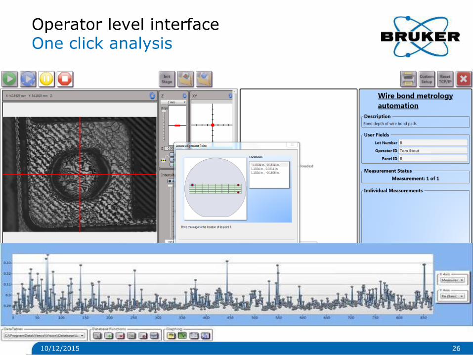
Printed Circuit Board HDI Development
10/12/2015 27

PCB key requirement Need longer working distance
10/12/2015 28
• First, some sample like the IC chip below requires working distance of > 1mm so that while measuring the die at the center, the objective will not crash at the molding compound.
• Secondly, it is more user friendly, operator will not crash the objective on the sample easily while focusing on the sample.
Z > 1 mm
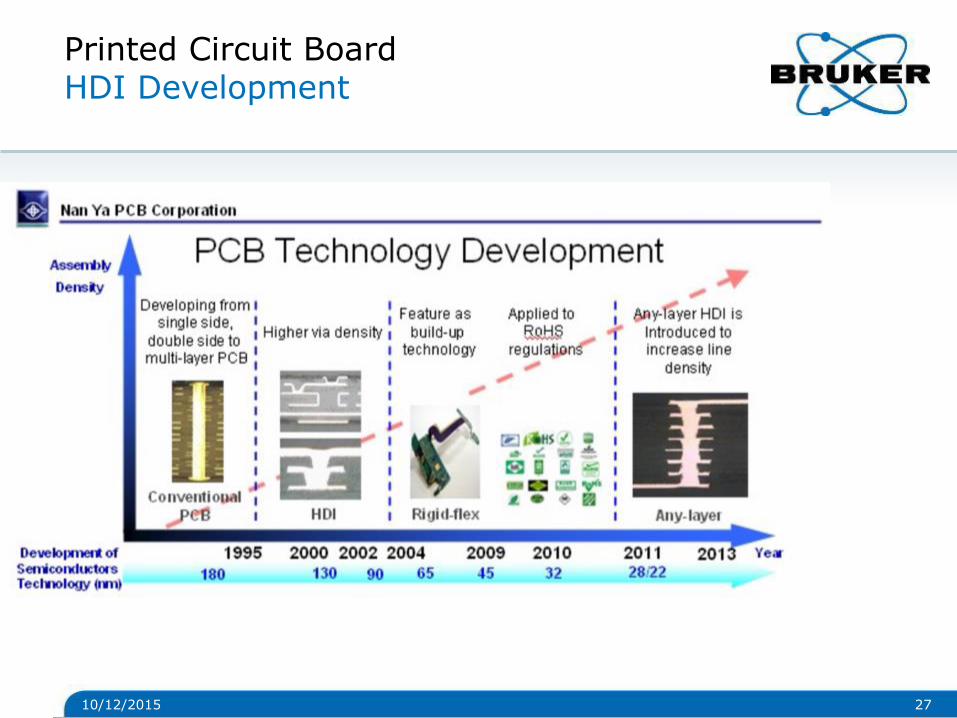
PCB key requirements Throughput
10/12/2015 29
One Image Acquisition
SPEED = Image Acquisition + Data Analysis
Multiple Analyses Same
Speed !!!
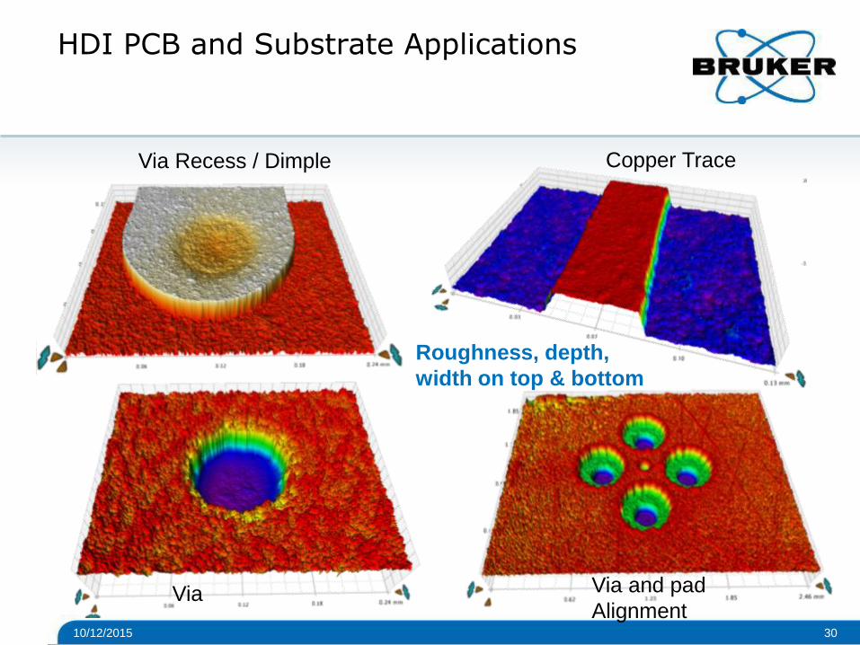
HDI PCB and Substrate Applications
10/12/2015 30
Via Recess / Dimple Copper Trace
Via Via and pad
Alignment
Roughness, depth,
width on top & bottom

Conclusion
10/12/2015 31
• White light interferometry profiler enables
• Undisturbed measurement over flexible membrane
• High throughput & accuracy
• Single characterization tool for all applications
In the field of flexible electronic and PCB
• Contrary to other optical technic, it has intrinsic benefits of constant sub-nm vertical resolution:
• Safer operation
• PCB ready measurement

© Copyright Bruker Corporation. All rights reserved.
www.bruker.com
Questions ?

Thank you for joining us
• Join the +PE mailing list
• Find out how to launch your own sponsored webinar
• Let us know your thoughts: [email protected]