Embed Size (px)
Citation preview
1
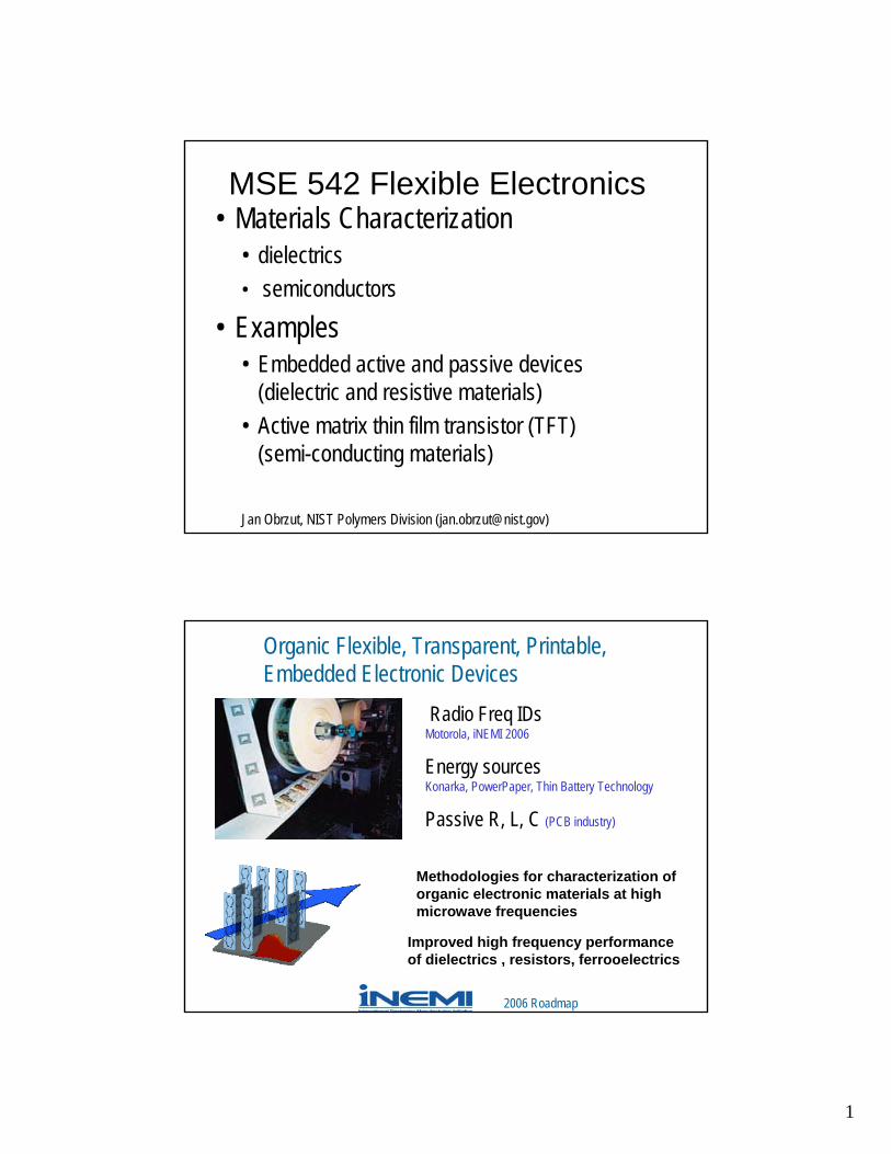
MSE 542 Flexible Electronics• Materials Characterization
• dielectrics • semiconductors
• Examples• Embedded active and passive devices
(dielectric and resistive materials) • Active matrix thin film transistor (TFT)
(semi-conducting materials)
Jan Obrzut, NIST Polymers Division ([email protected])
Radio Freq IDsMotorola, iNEMI 2006
Energy sourcesKonarka, PowerPaper, Thin Battery Technology
Passive R, L, C (PCB industry)
Organic Flexible, Transparent, Printable, Embedded Electronic Devices
Methodologies for characterization of organic electronic materials at high microwave frequencies
Improved high frequency performance of dielectrics , resistors, ferrooelectrics
2006 Roadmap
2
3
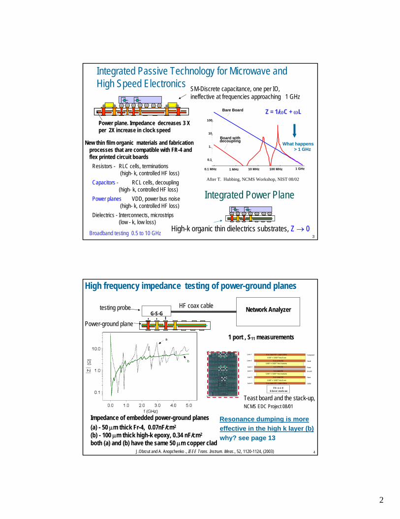
SM-Discrete capacitance, one per IO, ineffective at frequencies approaching 1 GHz
Power plane. Impedance decreases 3 X per 2X increase in clock speed
New thin film organic materials and fabrication processes that are compatible with FR-4 and flex printed circuit boards
Resistors - RLC cells, terminations (high- k, controlled HF loss)
Capacitors - RCL cells, decoupling (high- k, controlled HF loss)
Power planes VDD, power bus noise(high- k, controlled HF loss)
Dielectrics - Interconnects, microstrips(low - k, low loss)
Broadband testing 0.5 to 10 GHz
Integrated Passive Technology for Microwave and High Speed Electronics
0.1
1.
10.
100.
1 MHz 100 MHz0.1 MHz 1 GHz10 MHz
Bare Board
Board withdecoupling What happens
> 1 GHz
After T. Hubbing, NCMS Workshop, NIST 08/02
High-k organic thin dielectrics substrates, Z → 0
Z = 1/ωC + ωL
Integrated Power Plane
4
Impedance of embedded power-ground planes (a) - 50 μm thick Fr-4, 0.07nF/cm2
(b) - 100 μm thick high-k epoxy, 0.34 nF/cm2
both (a) and (b) have the same 50 μm copper clad
Resonance dumping is more effective in the high k layer (b)why? see page 13
G-S-G Network Analyzer
1 port , S11 measurements
testing probe HF coax cable
Power-ground plane
High frequency impedance testing of power-ground planes
½ oz copper foil + copper plating 0.020“ +/- 0.002” Tetra II core
0.020“ +/- 0.002” Tetra II core ½ oz copper foil + copper plating
½ oz copper foil
1 oz copper foil 1 oz copper foil
0.005“ +/- 0.001” Tetra II prepreg 0.005“ +/- 0.001” Tetra II prepreg
0.005“ +/- 0.001” Tetra II prepreg
½ oz copper foil Layer 1 Layer 2 Layer 3 Layer 4 Layer 5 Layer 6
Component Signal Power Ground Signa Solder
TV-1-1-Y 6-layer stack-up
Teast board and the stack-up, NCMS EDC Project 08/01
J.Obrzut and A. Anopchenko ., IEEE Trans. Instrum. Meas., 52, 1120-1124, (2003)

3
side view
top view
Microstrip, Zo
ZL
Via to GNP
G
S
G
Embedded Passive Device
Signal
Microstrip, Zo 1st level, S
2nd level, GNP 3rd level, S
4th level
Impedance, Zl , of Embedded Passive Devices
5
l0
cl/l rε
υτ 000 ==
τ0 - propagation time in the microstrip
εr - dielectric constant
Z0 - microstrip characteristic impedance
Zl - device impedance
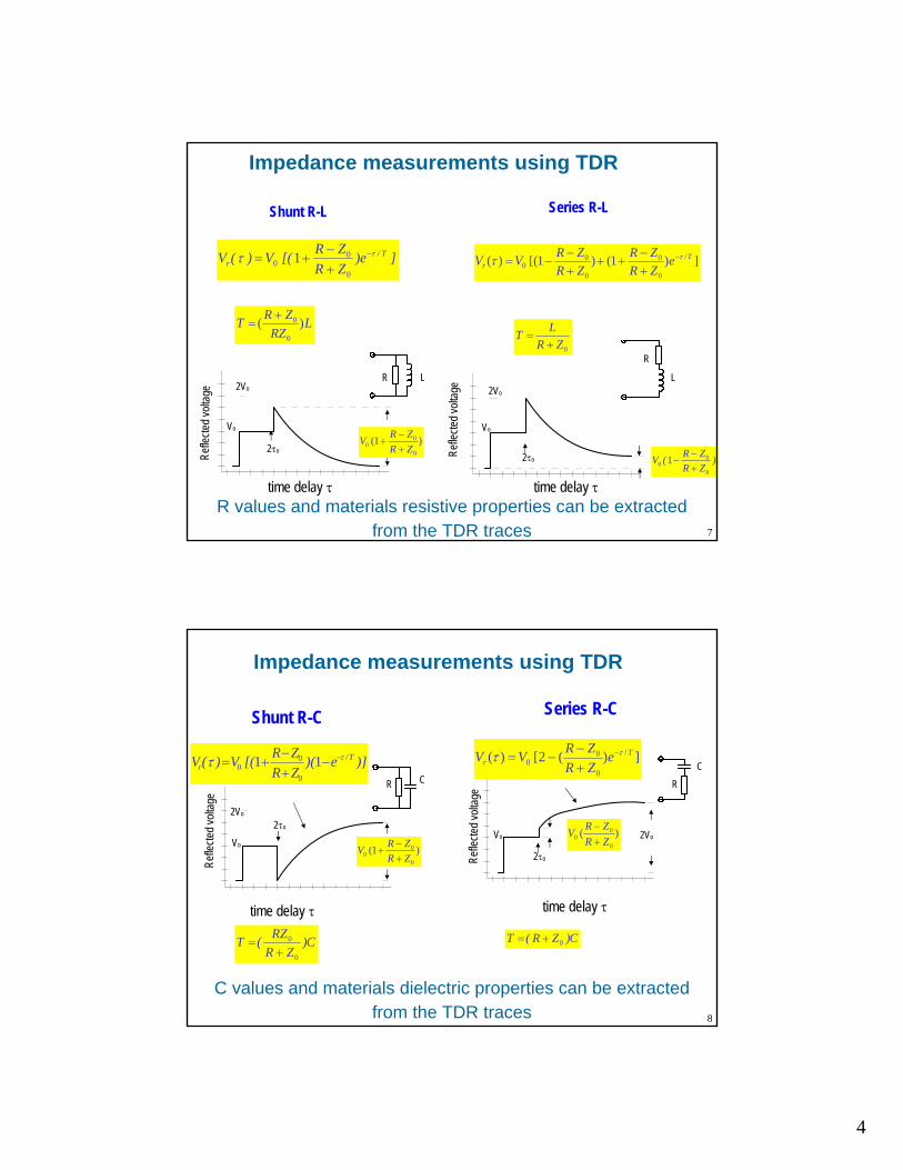
Impedance measurements using TDR
time delay
Refle
c ted v
ol ta g
e
Vo
time delay
Zl = 1/2 Zo
-1/3 Vo
Open, Zl = ∞
Refle
c ted v
ol ta g
e
Vo
Vr=Vo
Short, Zl = 0
Refle
c ted v
ol ta g
e
Vr = -V0
time delay
Vo
Reflected pulse is in phase, Vr = V0
Reflected pulse is out of phase, Vr = -V 0
For a matched impedance Zl = Zo Vr = Vo , no reflection
Refle
c ted v
ol ta g
e
Vr =+1/3 Vo
time delay
Vo
Resistor
Terminating standards
6
Resistive Load
2τo
2τo
2τo
2τo
l
l
ZZZZ
+−
=Γ0
0
0VVr=Γ
Γ−Γ+
=11
0ZZl
1−=Γ
1=Γ
31
=Γ
02ZZl =
31
−=Γ
021 ZZl =
Time Domain Application Theory, Agilent Application Note 1304-2
4
Refle
c ted v
ol ta g
e
Refle
c ted v
ol ta g
e2τo
2τo
2Vo
Vo Vo
R L
R
L
)1(0
00 ZR
ZRV+−
+
2Vo
)ZRZR(V
0
00 1
+−
−
]e)ZRZR[(V)(V T/
rττ −
+−
+=0
00 1 ])1()1[()( /
0
0
0
00
Tr e
ZRZR
ZRZRVV ττ −
+−
+++−
−=
Shunt R-L Series R-L
LRZ
ZRT )(0
0+=
0ZRLT+
=
7
Impedance measurements using TDR
time delay τ time delay τR values and materials resistive properties can be extracted
from the TDR traces
Vo
2Vo
2τoVo
2τoRefle
c ted v
ol ta g
e
Refle
c ted v
ol ta g
e
time delay τ time delay τ
R C RC
)1(0
00 ZR
ZRV+−
+2Vo)(
0
00 ZR
ZRV+−
])(2[)( /
0
00
Tr e
ZRZRVV ττ −
+−
−=
Shunt R-C Series R-C
8
Impedance measurements using TDR
)]e)(ZRZR[(V)(V T/
rττ −−
+−
+= 110
00
C)ZR
RZ(T0
0
+= C)ZR(T 0+=
C values and materials dielectric properties can be extracted from the TDR traces
5
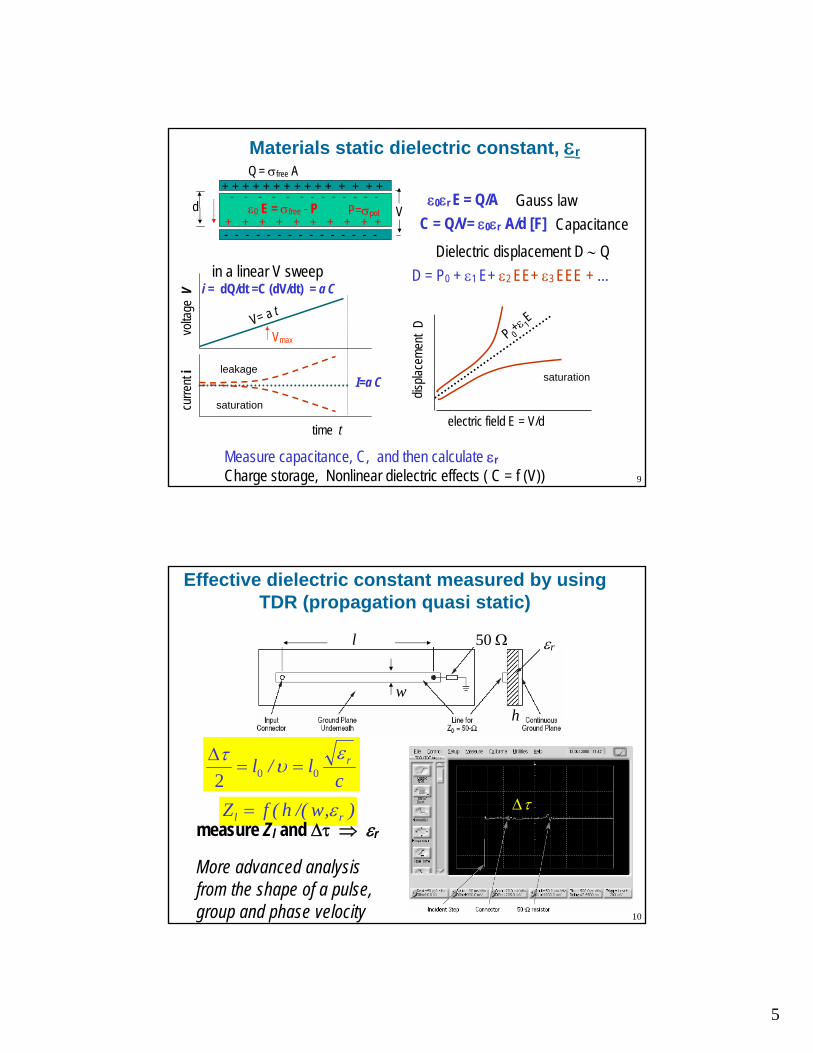
Gauss lawε0εr E = Q/AC = Q/V= ε0εr A/d [F]
D = P0 + ε1 E+ ε2 EE+ ε3 EEE + …
CapacitanceDielectric displacement D ∼ Q
in a linear V sweepi = dQ/dt =C (dV/dt) = a C
V= a t
time t
c urr e
n t i
v olta
ge V
Vmax
leakage
saturationd is
p lace
men t
D P 0+ε 1E
electric field E = V/d
saturationI=a C
Measure capacitance, C, and then calculate εr Charge storage, Nonlinear dielectric effects ( C = f (V))
Materials static dielectric constant, εr
d
Q = σfree A
V
+ + + + + + + + + + + + + + +
- - - - - - - - - - - - - - -+ + + + + + + + + +
ε0 E = σfree - P P=σpol
- - - - - - - - - - - - -
9
Effective dielectric constant measured by using TDR (propagation quasi static)
τΔc
l/l rευτ
002==
Δ
),w/(h(fZ rl ε=
l
w
εr
h
50 Ω
measure Zl and Δτ ⇒ εr
More advanced analysis from the shape of a pulse, group and phase velocity 10
6
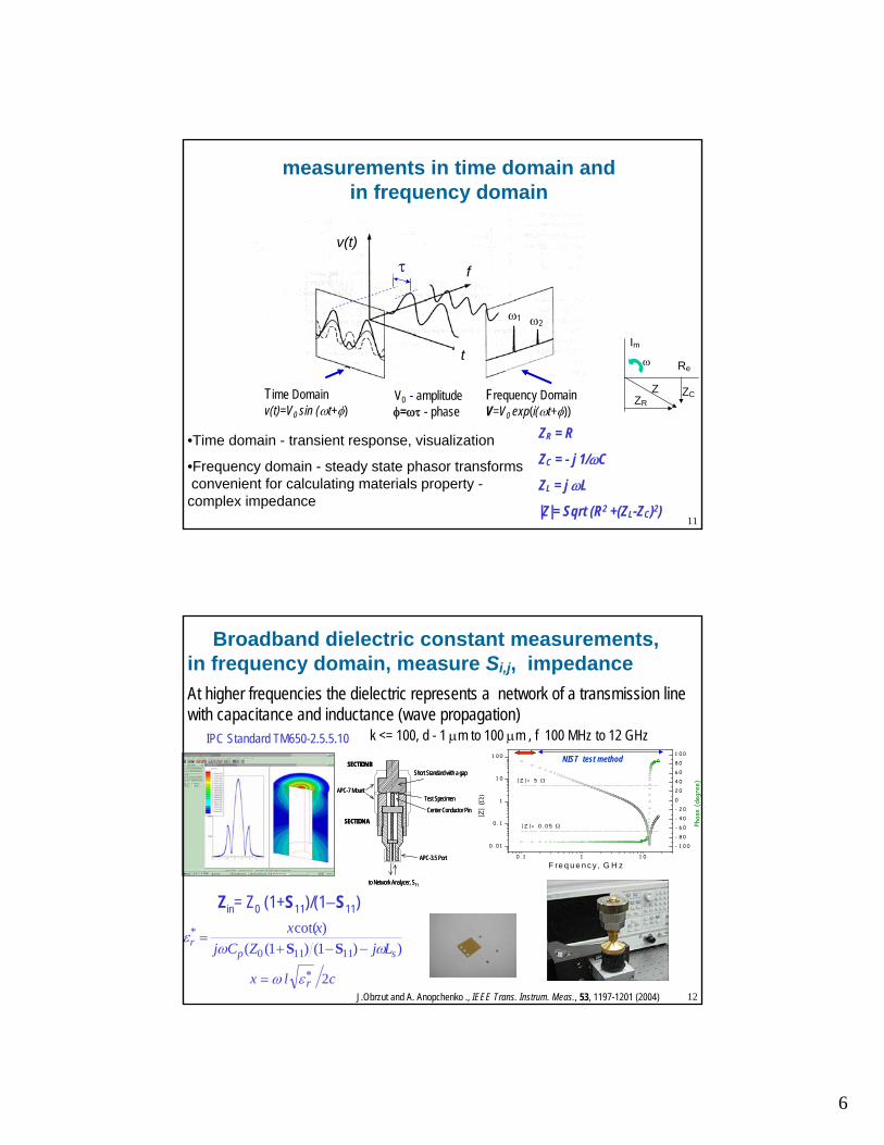
measurements in time domain and in frequency domain
ω1 ω2
τ
V0 - amplitudeφ=ωτ - phase
t
f
Frequency DomainV=V0 exp(i(ωt+φ))
Time Domainv(t)=V0 sin (ωt+φ)
v(t)
•Time domain - transient response, visualization
•Frequency domain - steady state phasor transformsconvenient for calculating materials property -complex impedance
ZR = R
ZC = - j 1/ωC
ZL = j ωL
|Z|= Sqrt (R2 +(ZL-ZC)2)
Z ZCZR
ω Re
Im
11
k <= 100, d - 1 μm to 100 μm , f 100 MHz to 12 GHz
At higher frequencies the dielectric represents a network of a transmission line with capacitance and inductance (wave propagation)
0 . 1 1 1 0
0 . 0 1
0 . 1
1
1 0
1 0 0
- 1 0 0
- 8 0
- 6 0
- 4 0
- 2 0
0
2 0
4 0
6 0
8 0
1 0 0
|Z |= 0 . 0 5 Ω
|Z |= 5 Ω
|Z|
(Ω)
F re q u e n c y, G H z
Phas
e (d
egre
e)
NIST test methodSECTION B
SECTION A
APC-7 Mount Test Specimen
Center Conductor Pin
APC-3.5 Port
to Network Analyzer, S11
Short Standard with a gapSECTION B
SECTION A
APC-7 Mount Test Specimen
Center Conductor Pin
APC-3.5 Port
to Network Analyzer, S11
Short Standard with a gap
IPC Standard TM650-2.5.5.10
))1()1(()cot(
11110
*
spr LjZCj
xxωω
ε−−+
=SS
clx r 2∗= εω
Zin= Z0 (1+S11)/(1−S11)
Broadband dielectric constant measurements, in frequency domain, measure Si,j, impedance
J.Obrzut and A. Anopchenko ., IEEE Trans. Instrum. Meas., 53, 1197-1201 (2004) 12

7
1
10
100
1000
0 10 20 30 40 50 60 70 80 90 100
BaTiO3 Concentration [vol%]
Die
lect
ric C
onst
ant
CR-SPEGDATMPTAEmCap
εBaTiO3
51%,130
Macromol. 34, 5910 (2001)
High frequency dielectric loss in in high k composites is beneficial for embedded capacitance applications, Z ≈ 0
Broadband dielectric constant of composite materials
13
a) l =164 mm, ε1 = 36.3 at 151 MHz, b) l=29.5 mm, ε1 = 36.4 at 842 MHz, c) l=8 mm, ε1 = 35.9 at 3.122 GHz
Dielectric constant measurements in frequency domain, measure S2,1 or S1,1 , resonant frequency
22
2
212
⎟⎠⎞
⎜⎝⎛+⎟
⎠⎞
⎜⎝⎛=
=⋅=
−= ⋅⋅−
wn
lmcf
nl/
)ee(EE
rn,m
gg
tto
ε
λλπβ
ββ
GSG
GSG
Z0 Z0ZR ≈ 1/2 Z0
a b c
NCMS EDC Project, 2000
l
14
8
• Low impedance power planes, R, L, C• TDR measurements, Z, Δτ ⇒ εr
• Static εr from charge/voltage capacitance• High frequency broadband ε* (to 12 GHz)
high k composites• Microstrip resonators, resonant frequency ⇒ ε*
• Nonlinear effects in organic dielectrics and semiconductors
Summary of dielectric materials characterization (Compared SMT ceramic passives vs embedded organic)
15
• has a non-volatile memory function that keeps its image stable.the screen image doesn't require repetitive updates to be maintained
• low power consumptionchanging content uses about the same amount of electricity as the weak radio waves found in some security badges.
• Uses TFT, Ferroelectric memory cell
Active matrix thin film transistor (TFT)
Tokyo International Forum 2005
Fujitsu bendable RGB color electronic paper
16
9
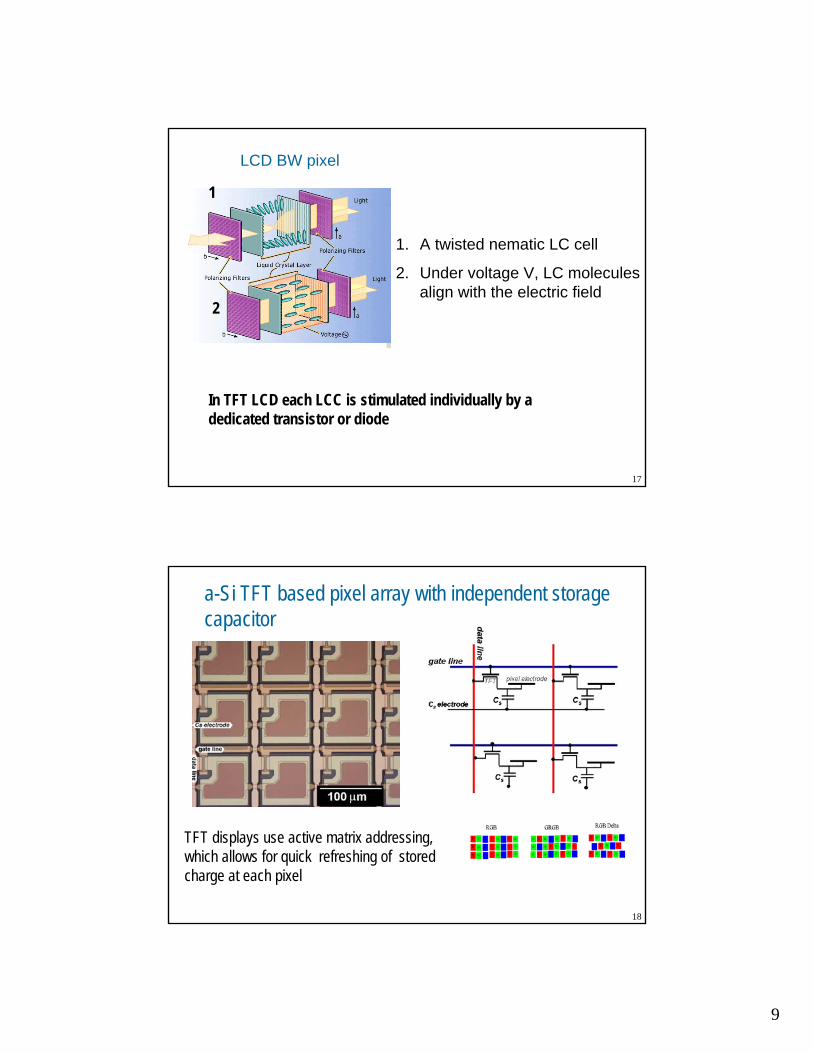
1. A twisted nematic LC cell
2. Under voltage V, LC molecules align with the electric field
LCD BW pixel
1
2
In TFT LCD each LCC is stimulated individually by a dedicated transistor or diode
17
a-Si TFT based pixel array with independent storage capacitor
TFT displays use active matrix addressing, which allows for quick refreshing of stored charge at each pixel
18
10
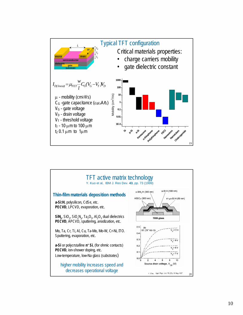
Typical TFT configuration
substrate
semiconductordrainsource
gatedielectric
t2W t3
t1
L
Critical materials properties:• charge carriers mobility• gate dielectric constant
Sip-S
ia-S
i
Pentac
ene
o-thio
phen
e
Polythi
ophe
ne F8T2
Nanow
ires
Nanotu
bes
Chalco
genid
e
1E-3
0.01
0.1
1
10
100
1000
Mob
ility
(cm
2 /Vs)
DTGGFET)linear(D V)VV(ClwI −=μ
μ - mobility (cm2/Vs)CG -gate capacitance (ε0εrA/t1)VG - gate voltageVD - drain voltageVT - threshold voltaget1 - 10 μm to 100 μmt2 0.1 μm to 1μm
19
TFT active matrix technologyY. Kuo et al, IBM J. Res Dev. 43, pp. 73 (1999)
Thin-film materials deposition methodsa-Si:H, polysilicon, CdSe, etc.PECVD, LPCVD, evaporation, etc.
SiNx, SiO2, SiOxNy, Ta2O5, Al2O3 dual dielectrics PECVD, APCVD, sputtering, anodization, etc.
Mo, Ta, Cr, Ti, Al, Cu, Ta-Mo, Mo-W, Cr-Ni, ITO. Sputtering, evaporation, etc.
a-Si or polycrstalline n+ Si, (for ohmic contacts) PECVD, ion-shower doping, etc. Low-temperature, low-Na glass (substrates)
higher mobility increases speed and decreases operational voltage
20
11
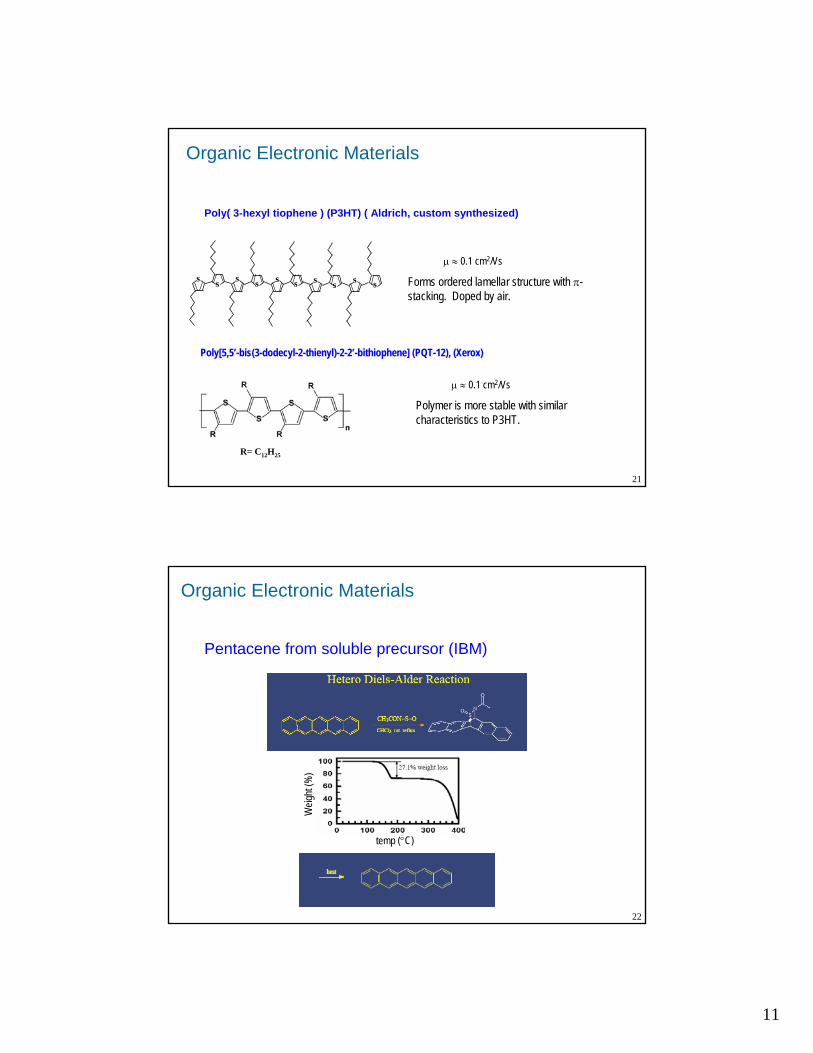
Organic Electronic Materials
Poly( 3-hexyl tiophene ) (P3HT) ( Aldrich, custom synthesized)
s s s ss s s s s s Forms ordered lamellar structure with π-stacking. Doped by air.
Poly[5,5’-bis(3-dodecyl-2-thienyl)-2-2’-bithiophene] (PQT-12), (Xerox)
Polymer is more stable with similar characteristics to P3HT.
R= C12H25
μ ≈ 0.1 cm2/Vs
μ ≈ 0.1 cm2/Vs
21
Organic Electronic Materials
Pentacene from soluble precursor (IBM)
Weig
ht (%
)
temp (°C)
22
12
Silicon Wafer
Cr/Au depositions and photolithography
Spin coat with polymer
Spin coat fabrication Process
Std chemical cleaning
Thermal oxidation (SiO2) orPulsed laser deposition (HfO2)
gate dielectric100 nm SiO2 or100 nm HfO2
Electrode pattern
(O2) plasma cleanHMDS
Contact angle 50°- 60°
Gate dielectric surface
preparation
0.5% solution in toluene
20 nm to 10 nm
Thermal treatment
Electrical Testing
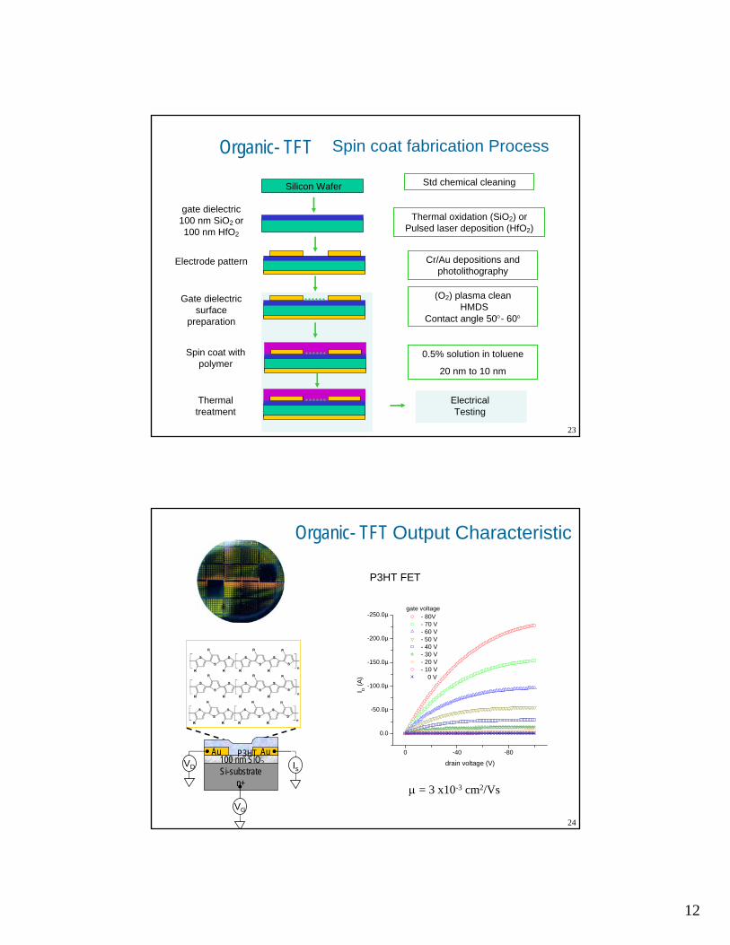
Organic- TFT
23
100 nm SiO2Si-substrate
n+
Au AuP3HT
VG
VD Is
20 nm to 60 nm
Organic- TFT Output Characteristic
P3HT FET
0 -40 -80
0.0
-50.0µ
-100.0µ
-150.0µ
-200.0µ
-250.0µ
I D (A
)
drain voltage (V)
- 80V - 70 V - 60 V - 50 V - 40 V - 30 V - 20 V - 10 V 0 V
gate voltage
μ = 3 x10⁻³ cm2/Vs
24

13
Vacuum deposited pentacene TFTμFET - 0.2 cm2/Vs
Charge carriers mobility increases with increasing molecular order
Organic- TFT
25
In organic semiconductors, both the properties of the individualmolecules and the structural order of the molecules in the film determine the macroscopic properties of the material.
These properties can be controlled by using molecular engineering to synthesize molecules with optimal characteristicsand by controlling the conditions under which these molecules assemble to form the solid.
Organic - TFT
26
14
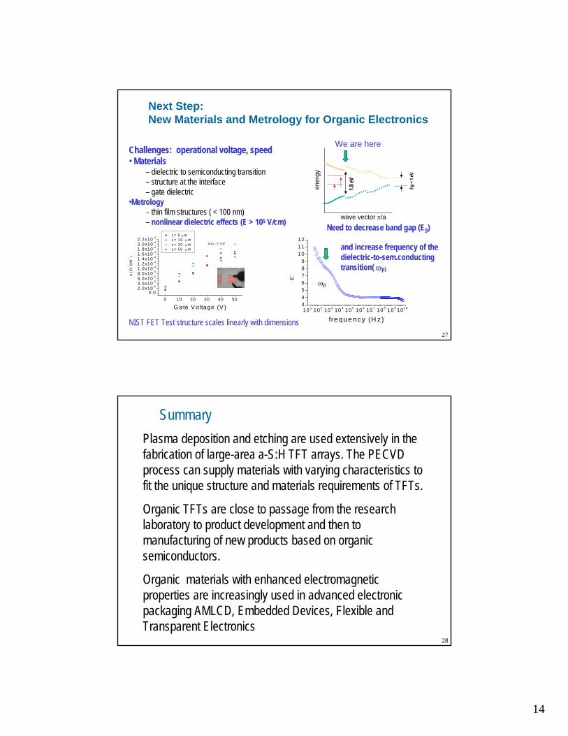
Next Step: New Materials and Metrology for Organic Electronics
Challenges: operational voltage, speed• Materials
– dielectric to semiconducting transition– structure at the interface– gate dielectric
•Metrology– thin film structures ( < 100 nm)– nonlinear dielectric effects (E > 105 V/cm) wave vector π/a
ener
g y
0 10 20 30 40 500.0
2.0x10-54 .0x10-56 .0x10-58 .0x10-51 .0x10-41 .2x10-41 .4x10-41 .6x10-41 .8x10-42 .0x10-42 .2x10-4
σ (Ω
−1cm
−1)
G ate Voltage (V )
L= 5 μm L= 10 μm L= 20 μm L= 50 μm
V d=-7 .5V
NIST FET Test structure scales linearly with dimensions10 1 10 2 10 3 10 4 10 5 10 6 10 7 10 8 10 9 10 10
3456789
101112
ε'
frequency (H z )
1.8 eV
Eg<
1 eV
We are here
ωp
Need to decrease band gap (Eg)
and increase frequency of the dielectric-to-sem.conducting transition( ωp)
27
Summary Plasma deposition and etching are used extensively in the fabrication of large-area a-S:H TFT arrays. The PECVD process can supply materials with varying characteristics to fit the unique structure and materials requirements of TFTs.
Organic TFTs are close to passage from the research laboratory to product development and then to manufacturing of new products based on organic semiconductors.
Organic materials with enhanced electromagnetic properties are increasingly used in advanced electronic packaging AMLCD, Embedded Devices, Flexible and Transparent Electronics
28