Embed Size (px)
Citation preview

Digital Design:Principles and Practices
Chapter 9Memory, CPLDs, and FPGAs

9.1 Read-Only Memory
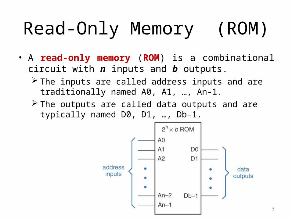
Read-Only Memory (ROM)• A read-only memory (ROM) is a combinational circuit with n
inputs and b outputs. The inputs are called address inputs and are traditionally named
A0, A1, …, An-1. The outputs are called data outputs and are typically named D0,
D1, …, Db-1.
3
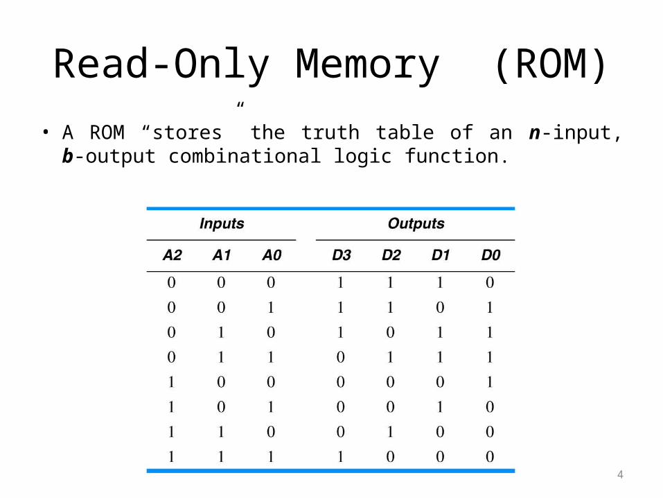
Read-Only Memory (ROM)
• A ROM “stores” the truth table of an n-input, b-output combinational logic function.
4
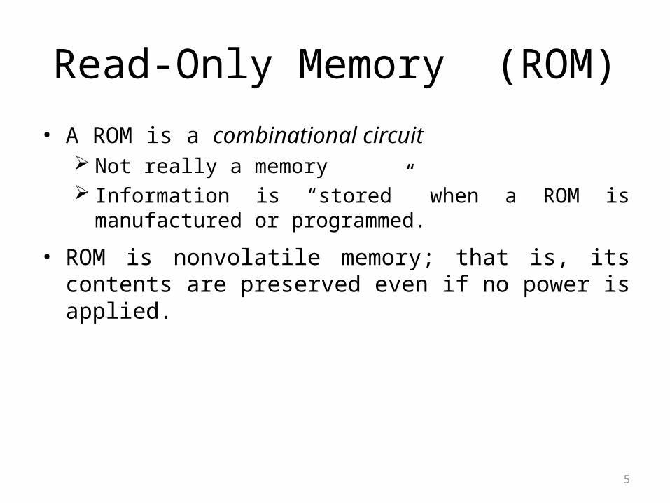
Read-Only Memory (ROM)
• A ROM is a combinational circuit Not really a memory Information is “stored” when a ROM is manufactured or
programmed.
• ROM is nonvolatile memory; that is, its contents are preserved even if no power is applied.
5
Nonvolatile Memory• ROM: hardwired during fabrication
• PROM (programmable ROM): can be programmed once only fuse
• EPROM (Erasable PROM): can be erased by UV light, and can be re-programmed Floating gate
• EEPROM (Electrically Erasable PROM): can be erased with on-chip circuitry Floating gate
• Flash memory: a variant of EEPROM that erases entire blocks rather than individual bits Floating gate
6
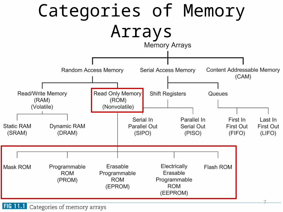
Categories of Memory Arrays
7
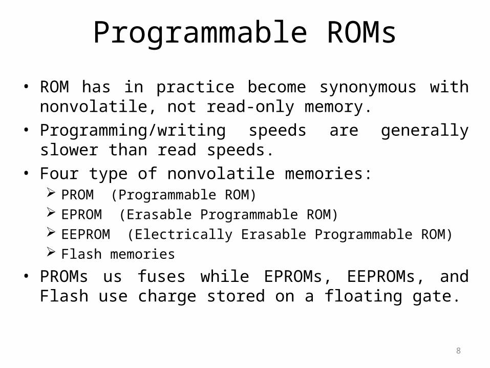
Programmable ROMs
• ROM has in practice become synonymous with nonvolatile, not read-only memory.
• Programming/writing speeds are generally slower than read speeds.
• Four type of nonvolatile memories: PROM (Programmable ROM) EPROM (Erasable Programmable ROM) EEPROM (Electrically Erasable Programmable ROM) Flash memories
• PROMs us fuses while EPROMs, EEPROMs, and Flash use charge stored on a floating gate.
8
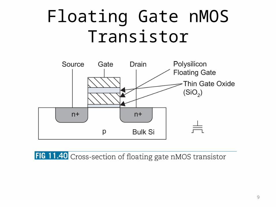
Floating Gate nMOS Transistor
9
Floating Gate nMOS Transistor• The floating gate is a good conductor, but it is not attached to
anything.
• Applying a high voltage to the upper gate causes electrons to jump through the thin oxide onto the floating gate.
• Injecting the electrons induces a negative voltage on the floating gate, effectively increasing the threshold voltage (Vt) of the transistor to the point that it is always OFF.
• EPROM: knock off the electrons off the floating gate by UV light
• EEPROM and Flash can be erased electrically.
10

9.2 Read/Write Memory

Read/Write Memory
• The name read/write memory (RWM) is given to memory arrays in which we can store and retrieve information at any time.
• Random-Access Memory (RAM) Static RAM (SRAM) Dynamic RAM (DRAM)
12

9.3 Static RAM
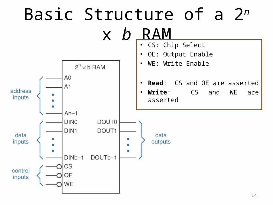
Basic Structure of a 2n x b RAM
14
• CS: Chip Select• OE: Output Enable• WE: Write Enable
• Read: CS and OE are asserted• Write: CS and WE are asserted
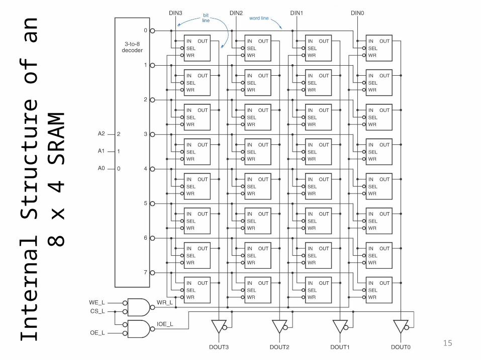
Inte
rnal
Str
uctu
re o
f an
8 x
4 SR
AM
15
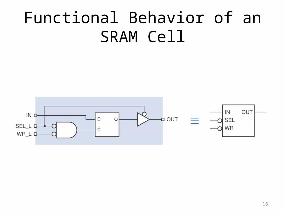
Functional Behavior of an SRAM Cell
16
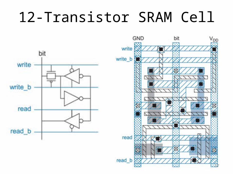
12-Transistor SRAM Cell
17
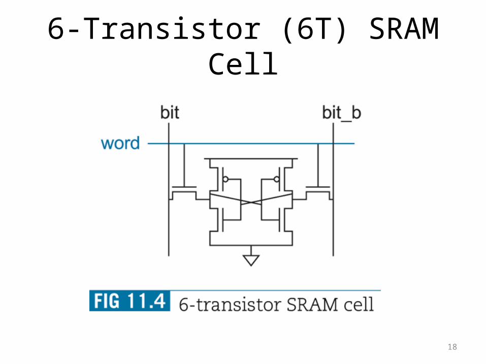
6-Transistor (6T) SRAM Cell
18
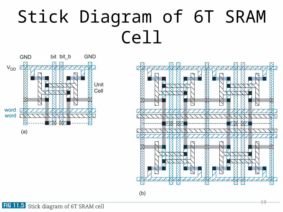
Stick Diagram of 6T SRAM Cell
19
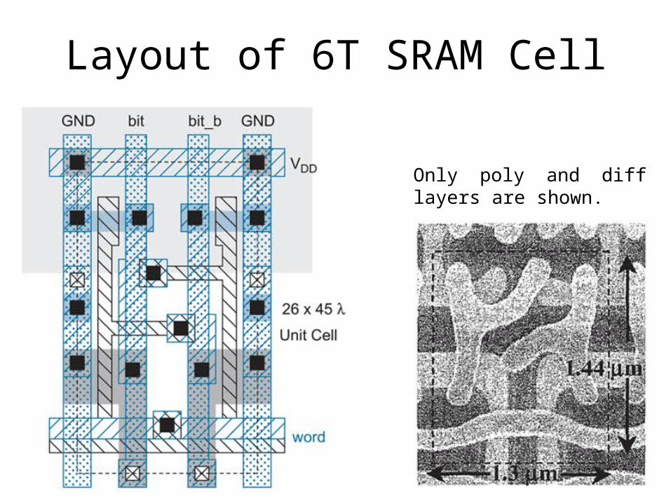
Layout of 6T SRAM Cell
20
Only poly and diff layers are shown.

9.4 Dynamic RAM
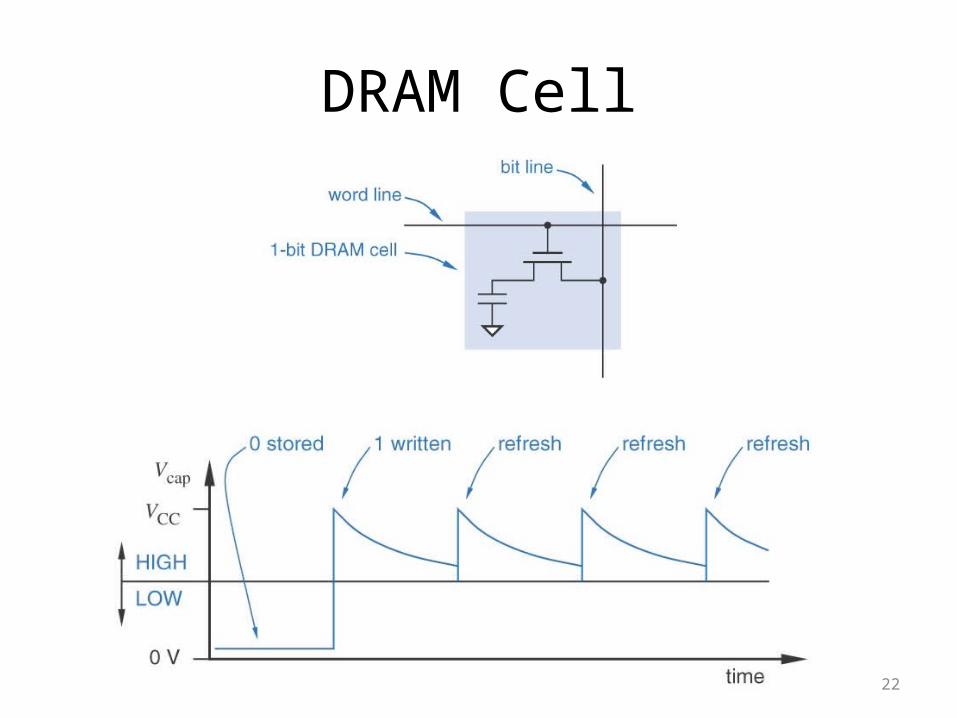
DRAM Cell
22
DRAM Cell
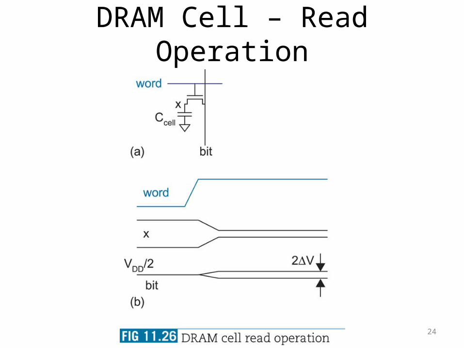
• A DRAM cell contains a transistor and a capacitor.
• A basic DRAM cell is substantially smaller than a SRAM cell, but the cell must be periodically read and refreshed so that its contents do not leak away.
• One a read, the bitline is first precharged to VDD/2. When the wordline rises, the capacitor shares its charge with the bitline, causing a voltage change △V that can be sensed. The read process disturbs the cell contents at x, so the cell must be rewritten after each read. [Figure 11.26] Sense amplifier
23
DRAM Cell – Read Operation
24
DRAM’s Capacitor
25
DRAM’s Capacitor
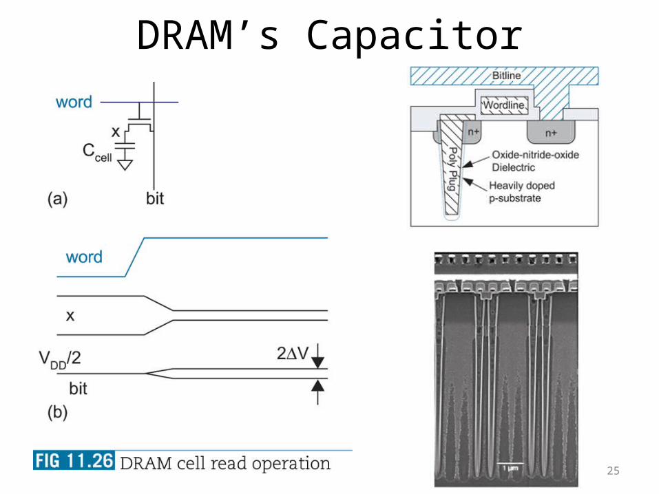
• A large cell capacitance (Ccell) is important to provide a reasonable voltage swing. It also is necessary to retain the contents of the cell for an acceptably long time.
• Specialized DRAM processes are required for manufacturing trench capacitors.
26