Embed Size (px)
Citation preview

Development of ASICs for multi-readout X-ray CCDs
Daisuke Matsuura
Department of Earth and Space Science, Graduate School of Science,
Osaka University, Japan
March 6, 2009

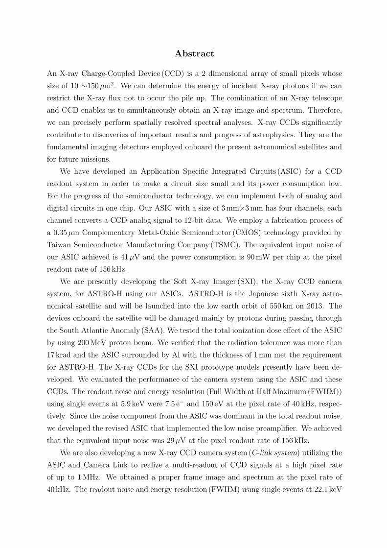
Abstract
An X-ray Charge-Coupled Device (CCD) is a 2 dimensional array of small pixels whose
size of 10 ∼150µm2. We can determine the energy of incident X-ray photons if we can
restrict the X-ray flux not to occur the pile up. The combination of an X-ray telescope
and CCD enables us to simultaneously obtain an X-ray image and spectrum. Therefore,
we can precisely perform spatially resolved spectral analyses. X-ray CCDs significantly
contribute to discoveries of important results and progress of astrophysics. They are the
fundamental imaging detectors employed onboard the present astronomical satellites and
for future missions.
We have developed an Application Specific Integrated Circuits (ASIC) for a CCD
readout system in order to make a circuit size small and its power consumption low.
For the progress of the semiconductor technology, we can implement both of analog and
digital circuits in one chip. Our ASIC with a size of 3mm×3mm has four channels, each
channel converts a CCD analog signal to 12-bit data. We employ a fabrication process of
a 0.35µm Complementary Metal-Oxide Semiconductor (CMOS) technology provided by
Taiwan Semiconductor Manufacturing Company (TSMC). The equivalent input noise of
our ASIC achieved is 41µV and the power consumption is 90mW per chip at the pixel
readout rate of 156 kHz.
We are presently developing the Soft X-ray Imager (SXI), the X-ray CCD camera
system, for ASTRO-H using our ASICs. ASTRO-H is the Japanese sixth X-ray astro-
nomical satellite and will be launched into the low earth orbit of 550 km on 2013. The
devices onboard the satellite will be damaged mainly by protons during passing through
the South Atlantic Anomaly (SAA). We tested the total ionization dose effect of the ASIC
by using 200MeV proton beam. We verified that the radiation tolerance was more than
17 krad and the ASIC surrounded by Al with the thickness of 1mm met the requirement
for ASTRO-H. The X-ray CCDs for the SXI prototype models presently have been de-
veloped. We evaluated the performance of the camera system using the ASIC and these
CCDs. The readout noise and energy resolution (Full Width at Half Maximum (FWHM))
using single events at 5.9 keV were 7.5 e− and 150 eV at the pixel rate of 40 kHz, respec-
tively. Since the noise component from the ASIC was dominant in the total readout noise,
we developed the revised ASIC that implemented the low noise preamplifier. We achieved
that the equivalent input noise was 29µV at the pixel readout rate of 156 kHz.
We are also developing a new X-ray CCD camera system (C-link system) utilizing the
ASIC and Camera Link to realize a multi-readout of CCD signals at a high pixel rate
of up to 1 MHz. We obtained a proper frame image and spectrum at the pixel rate of
40 kHz. The readout noise and energy resolution (FWHM) using single events at 22.1 keV

i
are 9.9 e− and 518 eV, respectively. We expect that C-link system enables anyone to easily
construct a compact readout system for X-ray CCDs with low noise and high pixel rate.

Contents
1 Introduction 1
2 X-ray CCDs 5
2.1 Output signal of an X-ray CCD . . . . . . . . . . . . . . . . . . . . . . . . 5
2.1.1 FDA . . . . . . . . . . . . . . . . . . . . . . . . . . . . . . . . . . . 5
2.1.2 N-channel and p-channel CCD signals . . . . . . . . . . . . . . . . . 8
2.2 Noise of an X-ray CCD . . . . . . . . . . . . . . . . . . . . . . . . . . . . . 9
2.2.1 White noise . . . . . . . . . . . . . . . . . . . . . . . . . . . . . . . 9
2.2.2 1/f noise . . . . . . . . . . . . . . . . . . . . . . . . . . . . . . . . . 10
2.3 Concept of the signal process for X-ray CCDs . . . . . . . . . . . . . . . . 11
2.3.1 Preamplifier . . . . . . . . . . . . . . . . . . . . . . . . . . . . . . . 11
2.3.2 Band-pass filter . . . . . . . . . . . . . . . . . . . . . . . . . . . . . 12
2.3.3 ADC . . . . . . . . . . . . . . . . . . . . . . . . . . . . . . . . . . . 16
2.4 Energy resolution . . . . . . . . . . . . . . . . . . . . . . . . . . . . . . . . 17
3 ASICs 19
3.1 Overview of ASICs . . . . . . . . . . . . . . . . . . . . . . . . . . . . . . . 19
3.2 Preamplifier . . . . . . . . . . . . . . . . . . . . . . . . . . . . . . . . . . . 20
3.2.1 Operational amplifier . . . . . . . . . . . . . . . . . . . . . . . . . . 22
3.3 5-bit DAC . . . . . . . . . . . . . . . . . . . . . . . . . . . . . . . . . . . . 24
3.4 ∆Σ ADC . . . . . . . . . . . . . . . . . . . . . . . . . . . . . . . . . . . . 29
3.4.1 Concept of ∆Σ ADCs . . . . . . . . . . . . . . . . . . . . . . . . . 29
3.4.2 ∆Σ ADC implemented in our ASICs . . . . . . . . . . . . . . . . . 34
3.5 Chain . . . . . . . . . . . . . . . . . . . . . . . . . . . . . . . . . . . . . . 41
3.5.1 Integral Non-Linearity (INL) . . . . . . . . . . . . . . . . . . . . . . 41
3.5.2 Noise performance . . . . . . . . . . . . . . . . . . . . . . . . . . . 42
3.6 Interface . . . . . . . . . . . . . . . . . . . . . . . . . . . . . . . . . . . . . 44
3.7 Development process of our ASICs . . . . . . . . . . . . . . . . . . . . . . 46
iii
iv CONTENTS
4 Performance of ASICs 47
4.1 Evaluation test system . . . . . . . . . . . . . . . . . . . . . . . . . . . . . 47
4.2 Integral Non-Linearity (INL) . . . . . . . . . . . . . . . . . . . . . . . . . . 49
4.3 Noise performance . . . . . . . . . . . . . . . . . . . . . . . . . . . . . . . 52
4.4 Power consumption . . . . . . . . . . . . . . . . . . . . . . . . . . . . . . . 53
4.5 Highest pixel rate . . . . . . . . . . . . . . . . . . . . . . . . . . . . . . . . 54
4.6 Radiation test . . . . . . . . . . . . . . . . . . . . . . . . . . . . . . . . . . 60
4.6.1 Motivation . . . . . . . . . . . . . . . . . . . . . . . . . . . . . . . . 60
4.6.2 Test condition . . . . . . . . . . . . . . . . . . . . . . . . . . . . . . 60
4.6.3 Test results . . . . . . . . . . . . . . . . . . . . . . . . . . . . . . . 61
4.7 Test summary . . . . . . . . . . . . . . . . . . . . . . . . . . . . . . . . . . 70
5 Performance of CCD camera systems using ASICs 75
5.1 Evaluation test setup . . . . . . . . . . . . . . . . . . . . . . . . . . . . . . 75
5.1.1 CCD-NeXT2 . . . . . . . . . . . . . . . . . . . . . . . . . . . . . . 76
5.1.2 Pch2k4k . . . . . . . . . . . . . . . . . . . . . . . . . . . . . . . . . 78
5.2 Test results . . . . . . . . . . . . . . . . . . . . . . . . . . . . . . . . . . . 78
5.3 Test results using 4 average method . . . . . . . . . . . . . . . . . . . . . . 89
6 High speed drive and readout system for X-ray CCDs 91
6.1 C-link system . . . . . . . . . . . . . . . . . . . . . . . . . . . . . . . . . . 91
6.1.1 Camera Link board . . . . . . . . . . . . . . . . . . . . . . . . . . . 91
6.1.2 DE I/F and ARM processor boards . . . . . . . . . . . . . . . . . 92
6.1.3 Driver, drain and video boards . . . . . . . . . . . . . . . . . . . . . 93
6.2 Performance of C-link system . . . . . . . . . . . . . . . . . . . . . . . . . 96
6.2.1 Unit testing . . . . . . . . . . . . . . . . . . . . . . . . . . . . . . . 96
6.2.2 Test using an X-ray CCD . . . . . . . . . . . . . . . . . . . . . . . 96
7 Summary 101
Acknowledgments 105
References 107
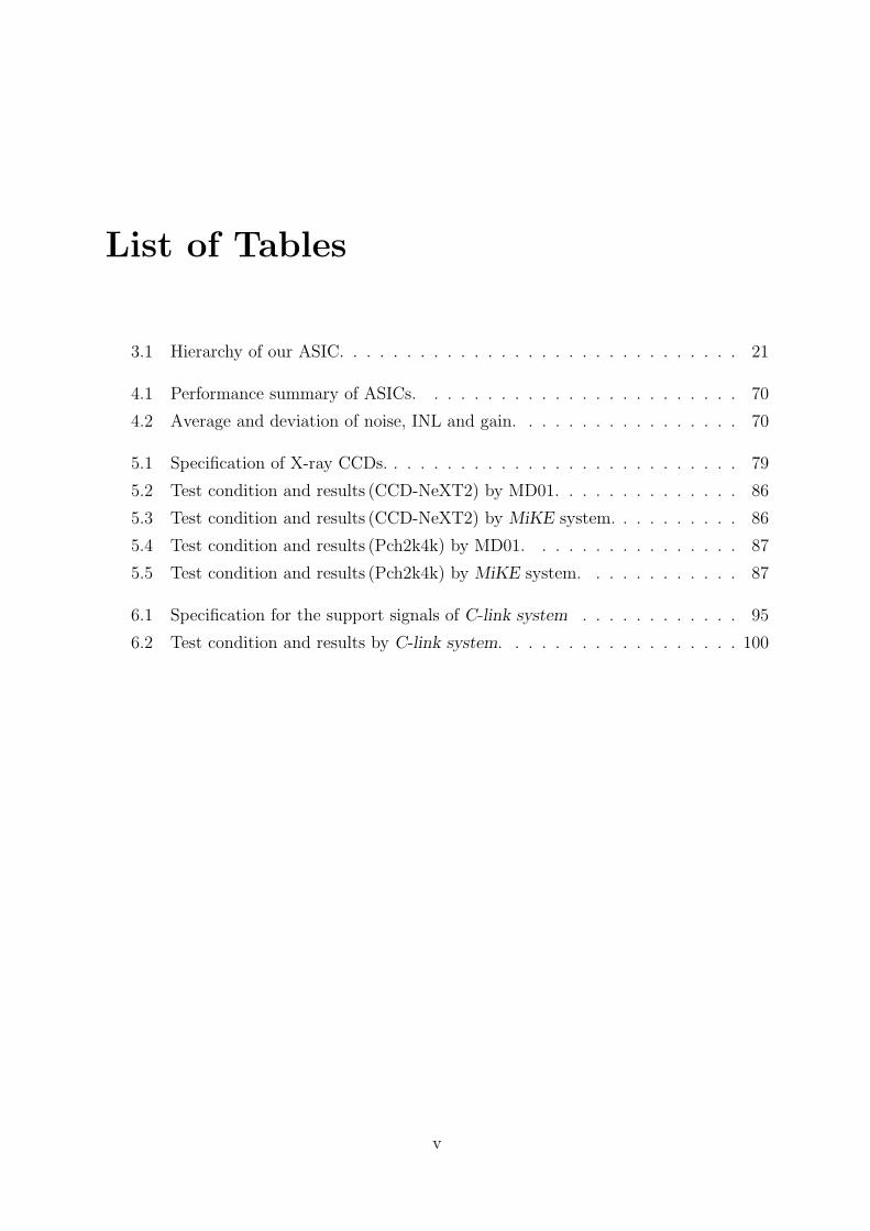
List of Tables
3.1 Hierarchy of our ASIC. . . . . . . . . . . . . . . . . . . . . . . . . . . . . . 21
4.1 Performance summary of ASICs. . . . . . . . . . . . . . . . . . . . . . . . 70
4.2 Average and deviation of noise, INL and gain. . . . . . . . . . . . . . . . . 70
5.1 Specification of X-ray CCDs. . . . . . . . . . . . . . . . . . . . . . . . . . . 79
5.2 Test condition and results (CCD-NeXT2) by MD01. . . . . . . . . . . . . . 86
5.3 Test condition and results (CCD-NeXT2) by MiKE system. . . . . . . . . . 86
5.4 Test condition and results (Pch2k4k) by MD01. . . . . . . . . . . . . . . . 87
5.5 Test condition and results (Pch2k4k) by MiKE system. . . . . . . . . . . . 87
6.1 Specification for the support signals of C-link system . . . . . . . . . . . . 95
6.2 Test condition and results by C-link system. . . . . . . . . . . . . . . . . . 100
v

List of Figures
2.1 Schematic view of a CCD device. . . . . . . . . . . . . . . . . . . . . . . . 6
2.2 Block diagram of the FDA. . . . . . . . . . . . . . . . . . . . . . . . . . . . 7
2.3 Signal waveforms of a n-channel and p-channel CCDs. . . . . . . . . . . . . 8
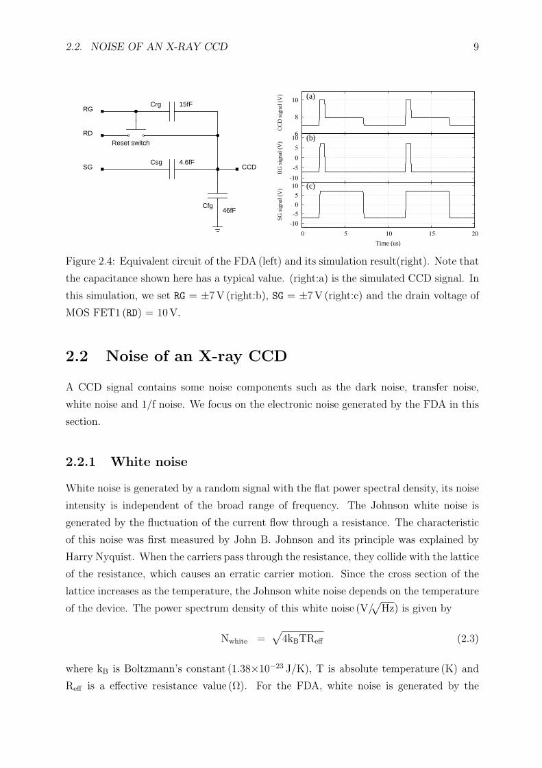
2.4 Equivalent circuit of the FDA and its simulation result. . . . . . . . . . . . 9
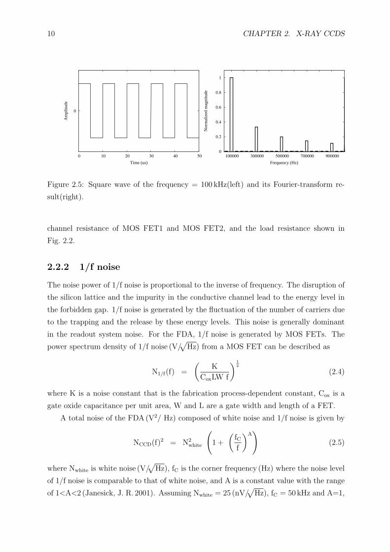
2.5 Square wave of the frequency = 100 kHz and its Fourier-transform result. . 10
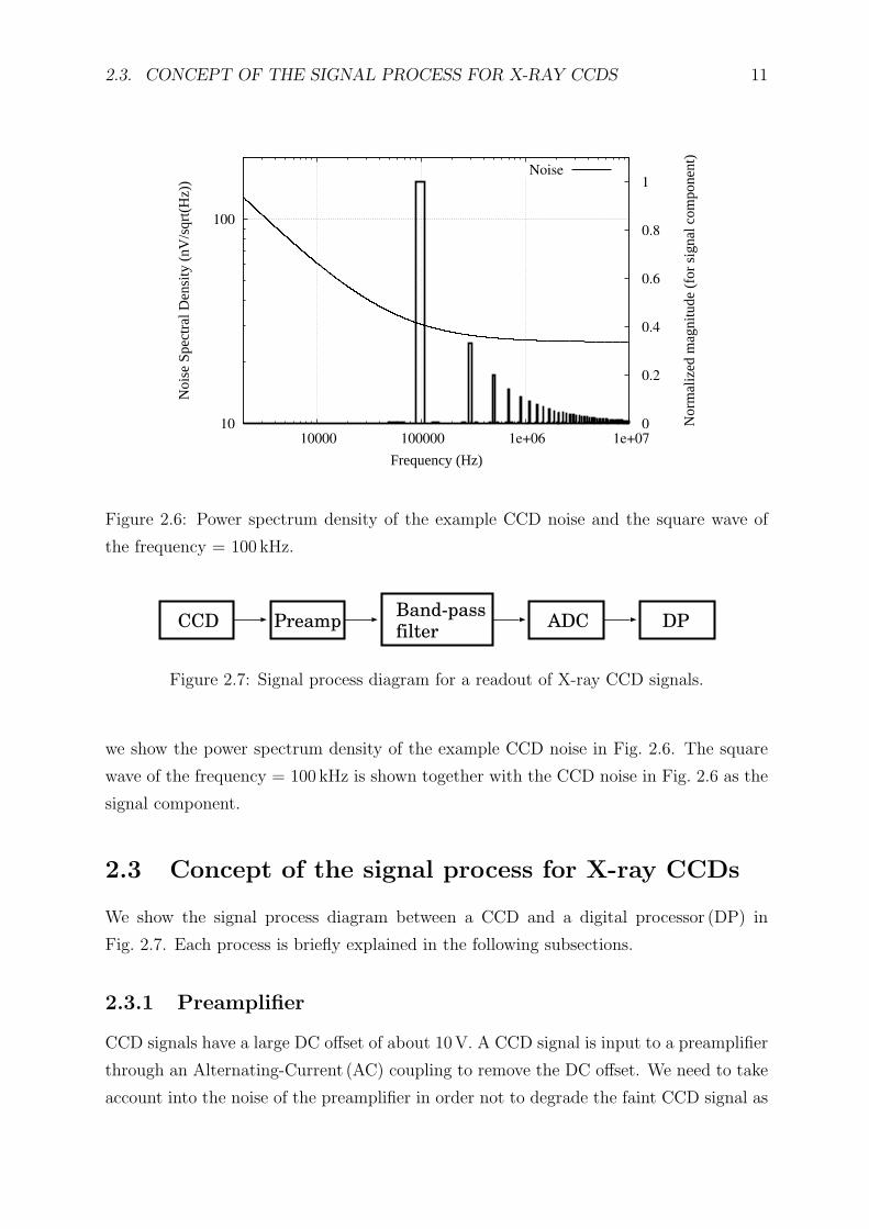
2.6 CCD noise spectrum density. . . . . . . . . . . . . . . . . . . . . . . . . . . 11
2.7 Signal process diagram for a readout of X-ray CCD signals. . . . . . . . . . 11
2.8 Concept of an iCDS method. . . . . . . . . . . . . . . . . . . . . . . . . . . 13
2.9 Equivalent noise charge in an iCDS method as a function of a pixel rate. . 14
2.10 Concept of a multi-sampling method. . . . . . . . . . . . . . . . . . . . . . 15
2.11 Equivalent noise charge in the multi-sampling method as a function of the
pixel rate. . . . . . . . . . . . . . . . . . . . . . . . . . . . . . . . . . . . . 16
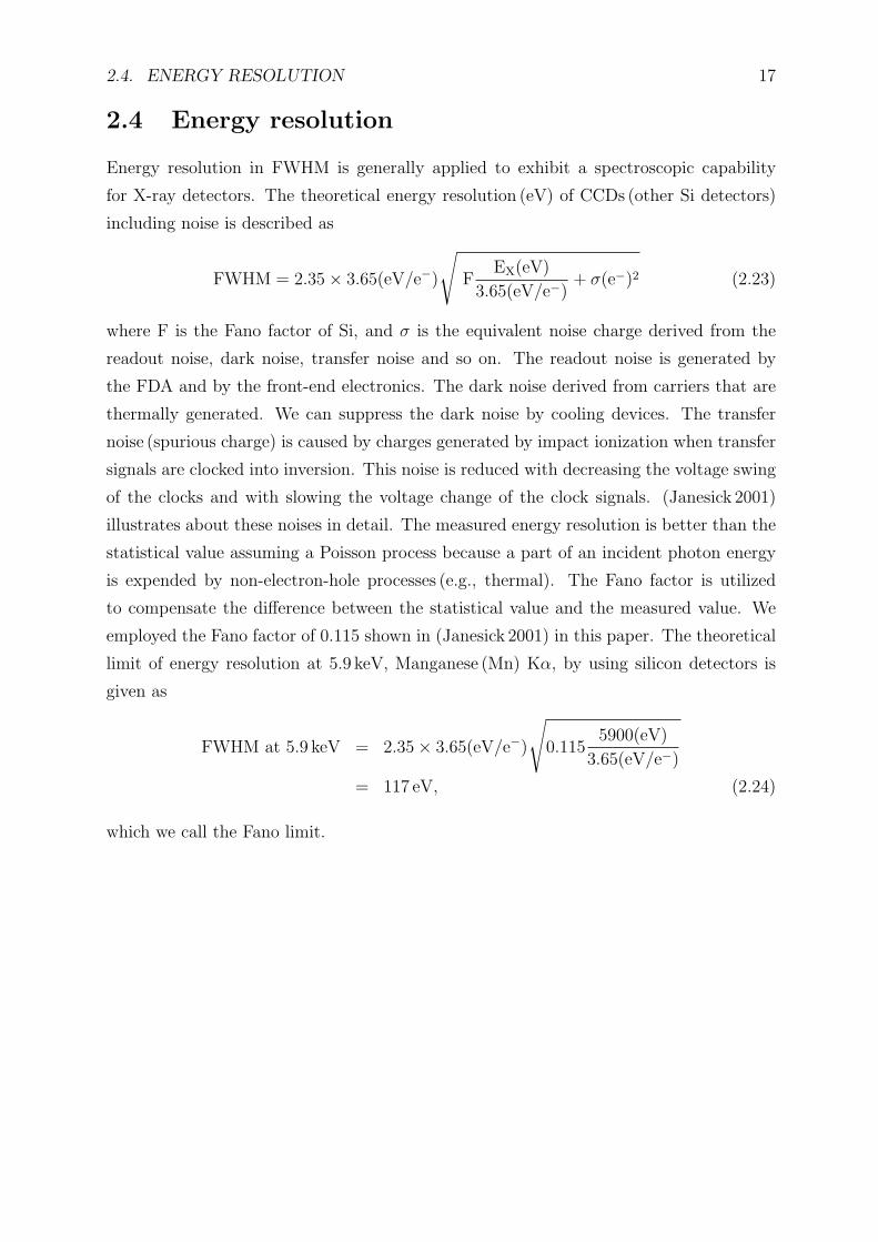
3.1 Data flow diagram of the readout system employing our ASIC. . . . . . . . 20
3.2 A photograph of the bare chip. . . . . . . . . . . . . . . . . . . . . . . . . 21
3.3 Block diagram of the preamplifier. . . . . . . . . . . . . . . . . . . . . . . . 23
3.4 Simulation result of the preamplifier. . . . . . . . . . . . . . . . . . . . . . 23
3.5 Block diagram of the operational amplifier. . . . . . . . . . . . . . . . . . . 24
3.6 Block diagram of the operational amplifier. . . . . . . . . . . . . . . . . . . 25
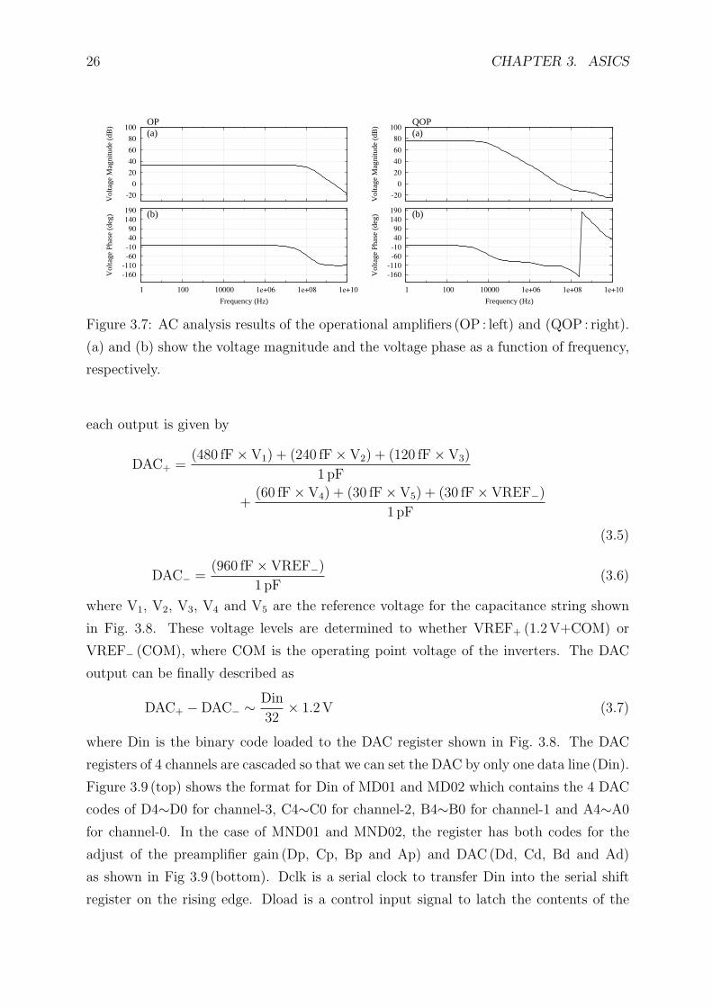
3.7 AC analysis results of the operational amplifiers. . . . . . . . . . . . . . . . 26
3.8 Block diagram of 5-bit DAC. . . . . . . . . . . . . . . . . . . . . . . . . . . 27
3.9 Data formats for the serial register of 5-bit DAC and preamplifier gain. . . 28
3.10 Simulation result of 5-bit DAC. . . . . . . . . . . . . . . . . . . . . . . . . 28
3.11 Block diagram of a basic first-order ∆Σ ADC. . . . . . . . . . . . . . . . . 30
3.12 Simulation results of ∆Σ ADC. . . . . . . . . . . . . . . . . . . . . . . . . 31
3.13 z-domain model for the first-order ∆Σ ADC shown in Fig. 3.11. . . . . . . 32
3.14 NTFs of first, second, third and fourth-order ∆Σ ADCs. . . . . . . . . . . 32
3.15 STFs of sinc, sinc2 and sinc3 filters. . . . . . . . . . . . . . . . . . . . . . . 35
vii
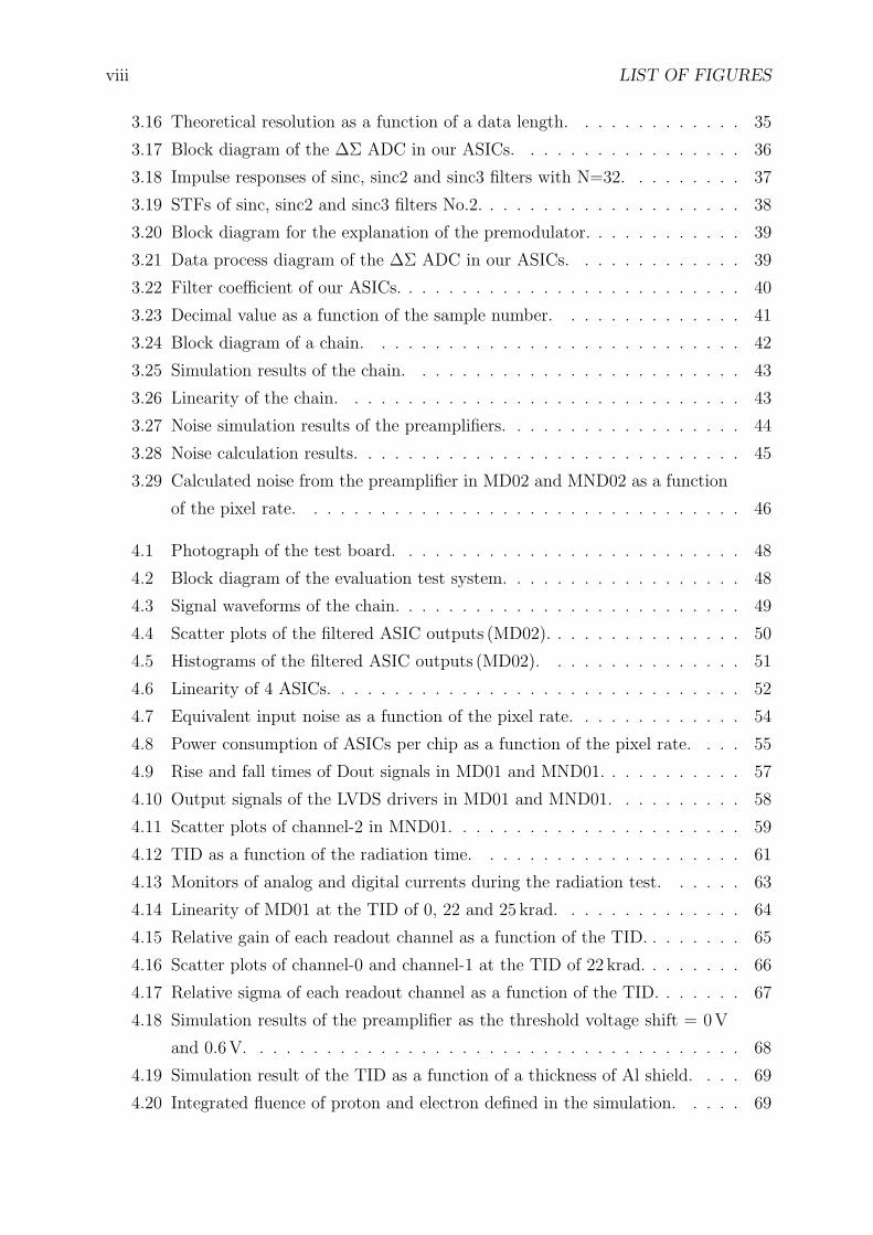
viii LIST OF FIGURES
3.16 Theoretical resolution as a function of a data length. . . . . . . . . . . . . 35
3.17 Block diagram of the ∆Σ ADC in our ASICs. . . . . . . . . . . . . . . . . 36
3.18 Impulse responses of sinc, sinc2 and sinc3 filters with N=32. . . . . . . . . 37
3.19 STFs of sinc, sinc2 and sinc3 filters No.2. . . . . . . . . . . . . . . . . . . . 38
3.20 Block diagram for the explanation of the premodulator. . . . . . . . . . . . 39
3.21 Data process diagram of the ∆Σ ADC in our ASICs. . . . . . . . . . . . . 39
3.22 Filter coefficient of our ASICs. . . . . . . . . . . . . . . . . . . . . . . . . . 40
3.23 Decimal value as a function of the sample number. . . . . . . . . . . . . . 41
3.24 Block diagram of a chain. . . . . . . . . . . . . . . . . . . . . . . . . . . . 42
3.25 Simulation results of the chain. . . . . . . . . . . . . . . . . . . . . . . . . 43
3.26 Linearity of the chain. . . . . . . . . . . . . . . . . . . . . . . . . . . . . . 43
3.27 Noise simulation results of the preamplifiers. . . . . . . . . . . . . . . . . . 44
3.28 Noise calculation results. . . . . . . . . . . . . . . . . . . . . . . . . . . . . 45
3.29 Calculated noise from the preamplifier in MD02 and MND02 as a function
of the pixel rate. . . . . . . . . . . . . . . . . . . . . . . . . . . . . . . . . 46
4.1 Photograph of the test board. . . . . . . . . . . . . . . . . . . . . . . . . . 48
4.2 Block diagram of the evaluation test system. . . . . . . . . . . . . . . . . . 48
4.3 Signal waveforms of the chain. . . . . . . . . . . . . . . . . . . . . . . . . . 49
4.4 Scatter plots of the filtered ASIC outputs (MD02). . . . . . . . . . . . . . . 50
4.5 Histograms of the filtered ASIC outputs (MD02). . . . . . . . . . . . . . . 51
4.6 Linearity of 4 ASICs. . . . . . . . . . . . . . . . . . . . . . . . . . . . . . . 52
4.7 Equivalent input noise as a function of the pixel rate. . . . . . . . . . . . . 54
4.8 Power consumption of ASICs per chip as a function of the pixel rate. . . . 55
4.9 Rise and fall times of Dout signals in MD01 and MND01. . . . . . . . . . . 57
4.10 Output signals of the LVDS drivers in MD01 and MND01. . . . . . . . . . 58
4.11 Scatter plots of channel-2 in MND01. . . . . . . . . . . . . . . . . . . . . . 59
4.12 TID as a function of the radiation time. . . . . . . . . . . . . . . . . . . . 61
4.13 Monitors of analog and digital currents during the radiation test. . . . . . 63
4.14 Linearity of MD01 at the TID of 0, 22 and 25 krad. . . . . . . . . . . . . . 64
4.15 Relative gain of each readout channel as a function of the TID. . . . . . . . 65
4.16 Scatter plots of channel-0 and channel-1 at the TID of 22 krad. . . . . . . . 66
4.17 Relative sigma of each readout channel as a function of the TID. . . . . . . 67
4.18 Simulation results of the preamplifier as the threshold voltage shift = 0V
and 0.6V. . . . . . . . . . . . . . . . . . . . . . . . . . . . . . . . . . . . . 68
4.19 Simulation result of the TID as a function of a thickness of Al shield. . . . 69
4.20 Integrated fluence of proton and electron defined in the simulation. . . . . 69
LIST OF FIGURES ix
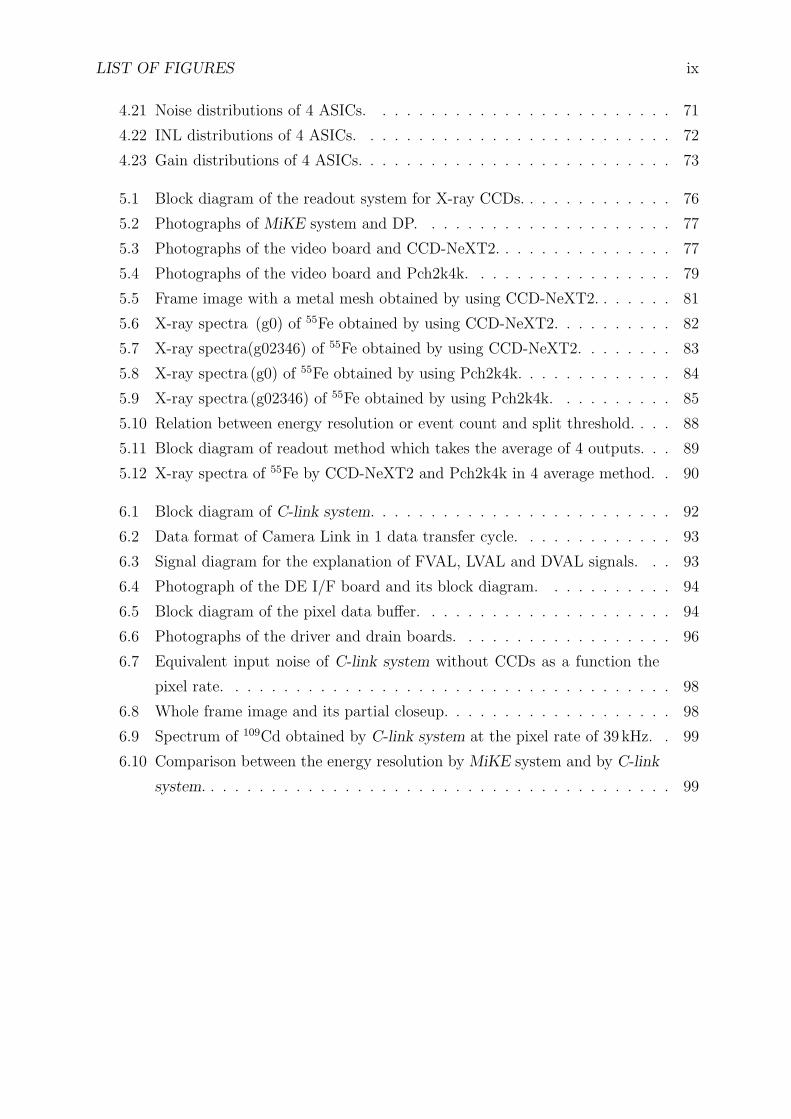
4.21 Noise distributions of 4 ASICs. . . . . . . . . . . . . . . . . . . . . . . . . 71
4.22 INL distributions of 4 ASICs. . . . . . . . . . . . . . . . . . . . . . . . . . 72
4.23 Gain distributions of 4 ASICs. . . . . . . . . . . . . . . . . . . . . . . . . . 73
5.1 Block diagram of the readout system for X-ray CCDs. . . . . . . . . . . . . 76
5.2 Photographs of MiKE system and DP. . . . . . . . . . . . . . . . . . . . . 77
5.3 Photographs of the video board and CCD-NeXT2. . . . . . . . . . . . . . . 77
5.4 Photographs of the video board and Pch2k4k. . . . . . . . . . . . . . . . . 79
5.5 Frame image with a metal mesh obtained by using CCD-NeXT2. . . . . . . 81
5.6 X-ray spectra (g0) of 55Fe obtained by using CCD-NeXT2. . . . . . . . . . 82
5.7 X-ray spectra(g02346) of 55Fe obtained by using CCD-NeXT2. . . . . . . . 83
5.8 X-ray spectra (g0) of 55Fe obtained by using Pch2k4k. . . . . . . . . . . . . 84
5.9 X-ray spectra (g02346) of 55Fe obtained by using Pch2k4k. . . . . . . . . . 85
5.10 Relation between energy resolution or event count and split threshold. . . . 88
5.11 Block diagram of readout method which takes the average of 4 outputs. . . 89
5.12 X-ray spectra of 55Fe by CCD-NeXT2 and Pch2k4k in 4 average method. . 90
6.1 Block diagram of C-link system. . . . . . . . . . . . . . . . . . . . . . . . . 92
6.2 Data format of Camera Link in 1 data transfer cycle. . . . . . . . . . . . . 93
6.3 Signal diagram for the explanation of FVAL, LVAL and DVAL signals. . . 93
6.4 Photograph of the DE I/F board and its block diagram. . . . . . . . . . . 94
6.5 Block diagram of the pixel data buffer. . . . . . . . . . . . . . . . . . . . . 94
6.6 Photographs of the driver and drain boards. . . . . . . . . . . . . . . . . . 96
6.7 Equivalent input noise of C-link system without CCDs as a function the
pixel rate. . . . . . . . . . . . . . . . . . . . . . . . . . . . . . . . . . . . . 98
6.8 Whole frame image and its partial closeup. . . . . . . . . . . . . . . . . . . 98
6.9 Spectrum of 109Cd obtained by C-link system at the pixel rate of 39 kHz. . 99
6.10 Comparison between the energy resolution by MiKE system and by C-link
system. . . . . . . . . . . . . . . . . . . . . . . . . . . . . . . . . . . . . . . 99

Chapter 1
Introduction
X-ray Charge-Coupled Devices (CCDs) are superior imaging detectors with excellent posi-
tional resolution (∼20 µm) and high quantum efficiency in an energy band of 0.2 keV∼10 keV,
where conventional X-ray mirrors are available as focusing devices. The X-ray CCD can
also work as spectrometers with moderate energy resolution (∼130 eV Full Width at Half
Maximum (FWHM) at 5.9 keV), when they are operated in the photon-counting mode.
The Solid state Imaging Spectrometers (SIS) on board the Japanese 4th X-ray as-
tronomy satellite, ASCA (Tanaka et al. 1994), were the first X-ray CCDs that were placed
in the focal plain of the X-ray focusing mirrors and worked as X-ray imaging spectrome-
ters. The ASCA SIS opened a new window in the field of X-ray astronomy, i.e., spatially
resolved spectroscopy of cosmic plasma with enough quality to diagnose elemental abun-
dances and ionization states, for which energy resolution of previous gas detectors were
not sufficient. For example, X-ray spectra of each position of a supernova remnant (SNR)
tell us not only the plasma temperatures but also their elemental abundances and ion-
ization states. These information are crucial to identify the origin of the plasmas and to
examine the progenitor of the remnant. Spatially resolved X-ray spectroscopy of diffuse
hot plasmas filled in elliptical galaxies and clusters of galaxies reveals the origin of heavy
elements in the universe. Spatial distribution of the plasma in these objects provides
evidence of dark matter which gravitationally binds those hot plasmas. Compact X-ray
sources, such as, neutron stars, black hole binaries, active galactic nuclei are also impor-
tant targets for X-ray CCD imaging spectrometers. Subsequent X-ray astronomy satellites
after ASCA employ the X-ray CCD, the Chandra ACIS (Garmire et al. 2003), the XMM-
Newton EPIC (Struder et al. 2001), (Turner et al. 2001) and the Suzaku XIS (Koyama et
al. 2007). Observations with these X-ray satellites have made progress in the X-ray imag-
ing spectroscopy of cosmic plasma, in its quality and variety, with many unprecedented
results.
1
2 CHAPTER 1. INTRODUCTION
A weak point of the X-ray CCD systems is, however, in their time resolution. Most
of the X-ray CCD systems mentioned above has a frame time of a few seconds, which can
be regarded as the time resolution of those systems. 1 The time resolution of the X-ray
CCDs is significantly lower than that of other photon counting X-ray detectors, such as gas
proportional counters, solid state detectors (typically 1µs or less), or micro calorimeters
(∼ ms). Rapid variabilities with time scales down to milliseconds are observed in compact
X-ray sources (black hole binaries, neutron star binaries) and have been an important
subjects in X-ray astronomy. Although various kinds of X-ray emitting pulsars have wide
range of pulsation periods, it ranges from a few milliseconds to several hundreds seconds.
Pulse phase resolved spectroscopy is a powerful tool to investigates those sources. The
time resolution of a few seconds will significantly restricts the targets for these kinds of
studies.
Another issue we have to consider for X-ray CCDs (and other photon-counting de-
tectors) is pile-up effects. In order to measure the energy of each X-ray photon with
X-ray CCDs, the number of photons entered into a pixel of the CCD during a frame time
must be one or zero. If two or more photons enter a pixel, i.e., pile-up, we cannot distin-
guish the event from that of a single photon with a higher energy, resulting in incorrect
spectra. This pile-up effect limits the maximum intensity of the targets which can be
observed in the photon-counting mode. The limit gets severer for the focusing mirrors
with better imaging quality and larger effective area. In fact, the pile-up effect hampers
observations of some bright sources with currently working X-ray satellites, Chandra,
XMM-Newton, and Suzaku. The condition will be much severer in future missions with
larger effective area, such as the International X-ray Observatory (IXO). This project su-
persedes both National Aeronautics and Space Administration’s (NASA’s) Constellation-
X (Bookbinder et al. 2008) and European Space Agency’s (ESA’s) X-ray Evolving Universe
Spectroscopy (XEUS) (Parmar et al. 2006) mission concepts. In order to reduce this pile-
up effect, i.e., to raise the intensity limit, we have to reduce the frame-time of the X-ray
CCD. It will be enabled by speeding up the readout time and/or increasing the number
of readout nodes. These two options are also needed to catch up with increasing size of
the X-ray CCD chips, reflecting the increasing size of the X-ray satellites.
These requirements are accelerating the development of fast X-ray CCD systems. The
noise level of the current X-ray CCD systems (e.g. Koyama et al. 2007, Miyata et al. 2006)
1ASCA SIS and most of other X-ray CCDs on board X-ray astronomy satellites can be operated in a
special observation mode for fast timing observations. In the case of the ASCA SIS, Fast mode prepared
for that purpose could realize 16ms time resolution. Nevertheless, imaging information in this mode is
one dimensional and the target is limited to a bright point-like source.
3
realizes energy resolution as good as the theoretical limit (Fano limit). However, the pixel
rate is limited up to about 100 kHz without degradation of the readout noise. Since current
X-ray CCDs have typically ∼105 pixels per readout node, we cannot expect reducing the
frame time by an order magnitude with current systems. Increasing the number of readout
nodes to, for example, 100 will be a solution. However, in this case, the size and electric
power needed is unrealistic for space use, if we simply employ 100 units of the current
CCD electronics systems which are constructed with discrete electronic components.
We thus have started developing of an Application Specific Integrated Circuits (ASIC)
for multi-readout X-ray CCDs. An ASIC is a key technology to realize multi-channel
readout systems for pixel and strip detectors. Another reason behind present ASIC de-
velopments is that foundries provide a multi-project wafer run with relatively low price.
Some institutes have been developing ASICs for the readout of CCDs. In X-ray re-
gion, the CMOS Amplifier and MultiplEXer (CAMEX) chip was employed as the readout
system for pnCCDs onboard XMM-Newton (Struder et al. 2001). The revised CAMEX
will be employed for the eROSITA X-ray telescope (Herrmann et al. 2007). The ASIC
with the size of 9mm×6mm has 128 analog readout channels. Each channel consists
of a Junction Field Effect Transistor (JFET)-amplifier, low-pass filter, 8-fold Correlated
Double Sampling (CDS) circuit and sample & hold circuit. A multiplexer is connected
to each channel and transmits the analog data of 128 channels to an Analog-to-Digital
Converter (ADC) off the chip. An image area of the CCD is 384 × 384 pixels, and each
column has a readout node that is connected to the CAMEX chip. Its frame rate of a full
image mode is 20Hz. In visible region, a team in the Lawrence Berkeley National Labora-
tory developed an ASIC for the Super Nova-Acceleration Probe (SNAP) satellite (Karcher
et al. 2007). The number of channel is 4 and each channel consists of a preamplifier, CDS
circuit and pipeline ADC. This chip has an excellent low noise of 6.2µV at the pixel rate
of 100 kHz and low power consumption of 121mW.
Our first ASIC had two readout channels and each channel consisted of an integrated
Correlated Double Sampling (iCDS) circuit and slope ADC (Matsuura et at. 2007). A
noise level of this ASIC was about 10 times worse than our requirement of several electrons.
We decided to develop a new type of ASIC that employed a ∆Σ ADC(Inose et al. 1962)
instead of the iCDS circuit and slope ADC (Doty patent 2006a), (Doty et al. 2006b). An
outline of our ASICs is described in Chapter 3. Their teat results by using pseudo signals
are summarized in Chapter 4.
We are presently designing an X-ray CCD camera system for the Soft X-ray Im-
ager (SXI) (Tsunemi et al. 2008) onboard ASTRO-H (Takahashi et al. 2008) employing
our ASICs. ASTRO-H is the Japanese sixth X-ray astronomical mission following to
4 CHAPTER 1. INTRODUCTION
Suzaku (Mitsuda et al. 2007), and will be launched in 2013. In the SXI, all components
of the CCD camera system, such as CCDs, cooling device, drive and readout systems,
are developed in Japan. We evaluated performances of camera systems using the ASIC
and X-ray CCDs of prototype models for the SXI in Chapter 5. We are also developing
another readout system with low noise and high pixel rate using the ASIC for ground
experiments as shown in Chapter 6.
Chapter 2
X-ray CCDs
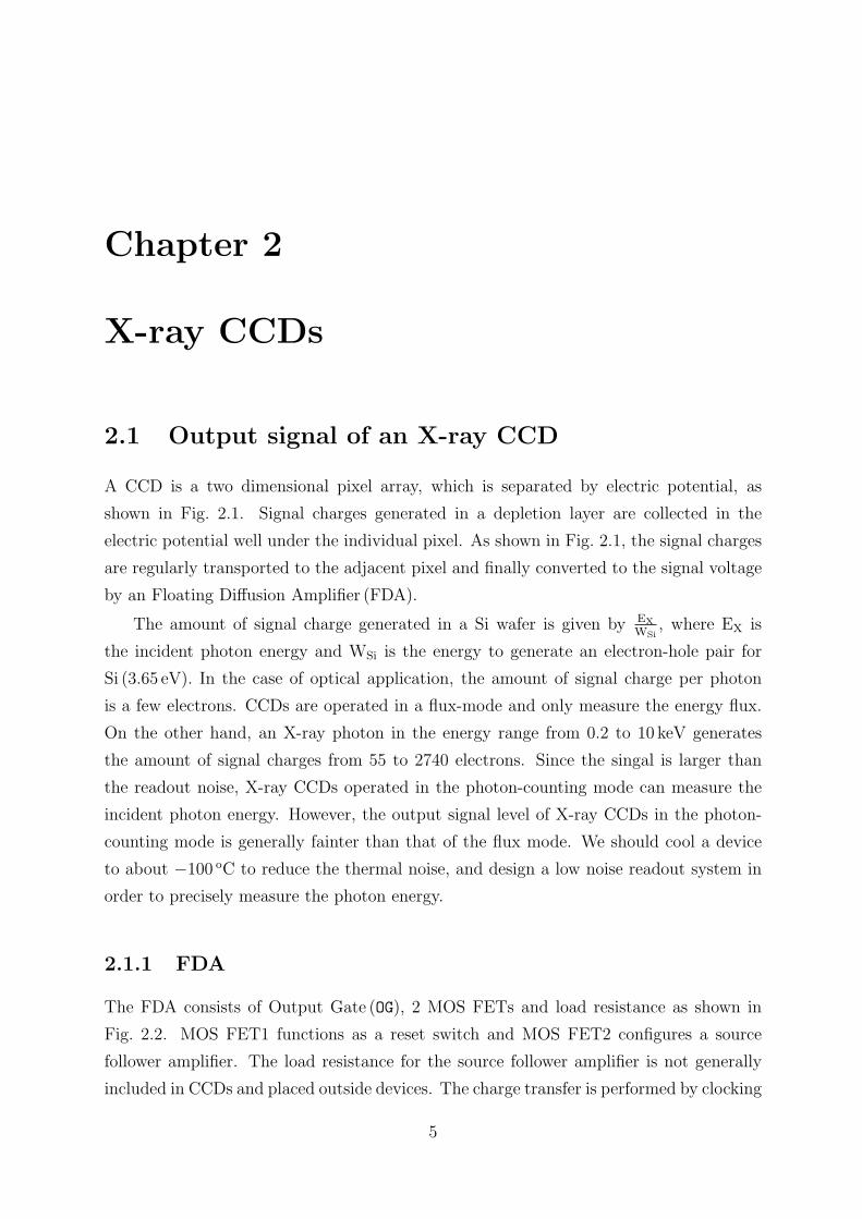
2.1 Output signal of an X-ray CCD
A CCD is a two dimensional pixel array, which is separated by electric potential, as
shown in Fig. 2.1. Signal charges generated in a depletion layer are collected in the
electric potential well under the individual pixel. As shown in Fig. 2.1, the signal charges
are regularly transported to the adjacent pixel and finally converted to the signal voltage
by an Floating Diffusion Amplifier (FDA).
The amount of signal charge generated in a Si wafer is given by EX
WSi, where EX is
the incident photon energy and WSi is the energy to generate an electron-hole pair for
Si (3.65 eV). In the case of optical application, the amount of signal charge per photon
is a few electrons. CCDs are operated in a flux-mode and only measure the energy flux.
On the other hand, an X-ray photon in the energy range from 0.2 to 10 keV generates
the amount of signal charges from 55 to 2740 electrons. Since the singal is larger than
the readout noise, X-ray CCDs operated in the photon-counting mode can measure the
incident photon energy. However, the output signal level of X-ray CCDs in the photon-
counting mode is generally fainter than that of the flux mode. We should cool a device
to about −100 oC to reduce the thermal noise, and design a low noise readout system in
order to precisely measure the photon energy.
2.1.1 FDA
The FDA consists of Output Gate (OG), 2 MOS FETs and load resistance as shown in
Fig. 2.2. MOS FET1 functions as a reset switch and MOS FET2 configures a source
follower amplifier. The load resistance for the source follower amplifier is not generally
included in CCDs and placed outside devices. The charge transfer is performed by clocking
5
6 CHAPTER 2. X-RAY CCDS
sirial shift registor
imaging area
charge transfer direction(horizontal)
char
ge
tran
sfer
dir
ecti
on(v
erti
cal)
FDA
Figure 2.1: Schematic view of a full-frame CCD device.
gate voltages such as the horizontal transfer gate (P1H) and Summing Gate (SG). We supply
a Direct-Current (DC) voltage to OG for the separation between SG and Floating Gate (FG)
when SG is clocked high. Sense capacitance (Cs) converts the transferred charges to the
voltage signal. Cs is determined from a node capacitance of FG, gate capacitance of MOS
FET2 and neighboring parasitic capacitances (Janesick, J. R. 2001). The conversion factor
of CCDs can be described as
Sv =q
Cs
(2.1)
where Sv is the conversion factor (µV/e−) and q is the elementary electric charge (1.6×10⁻¹⁹
coulombs). Since Sv is a order of several (µV/e−), we find that Cs is designed to be an
order of several 10 fF.
Fig. 2.2(1)∼(3) illustrate the operation of the FDA including Reset Gate (RG), SG and
P1H during 1 pixel readout time. Signal waveforms of CCDs after an amplifier with a gain
of 10 are shown in Fig. 2.3. There are 3 voltage levels in a CCD signal, which we call a
reset, floating and signal levels. These voltage levels are generated in each operation of
the FDA shown in Fig. 2.2(1)∼(3). Fig. 2.2(1)(2) show the reset operation of FG. There
are the signal charges of the previous pixel in FG in Fig. 2.2(1). These charges are passed
through MOS FET1 when RG is clocked high, and FG is reset as shown in Fig. 2.2(2).
Figure 2.4 shows the equivalent circuit of the FDA and its simulation. Since Cs and a
gate to source capacitance of MOS FET1 (Crg) shown in Fig. 2.4 (left) divides the clock
signal of RG, the voltage of FG is determined by the drain voltage of MOS FET1 (RD) and
the RG feed-through pulse as shown in Fig. 2.4 (right) during the reset operation. These
voltage levels of FG correspond to the reset and floating levels in Fig. 2.3. As shown in
Fig. 2.2 (c), the signal charges in SG are transferred to FG when SG is clocked low. The
2.1. OUTPUT SIGNAL OF AN X-RAY CCD 7
P1H SG
RG
MOS FET 1
MOS FET 2
pote
nti
al
RG
MOS FET 1
MOS FET 2
RG : High
RG : Low
SG : HighP1H : Low
P1H : Low SG : High
RG
MOS FET 1
MOS FET 2
RG : Low
P1H : High SG : Low
p+
output
output
output
elec
tron
s
signal charges
p+
OG
RD
OD
P1H SG OG
P1H SG OG
RD
OD
OD
RD
(1)
(2)
(3)
pote
nti
alp
ote
nti
alFG
FG
FG
Figure 2.2: Block diagram of the FDA and its operation.
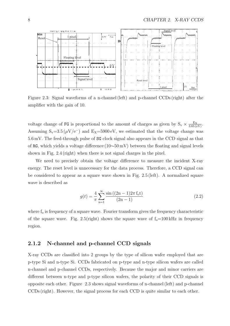
8 CHAPTER 2. X-RAY CCDS
Floating level
Reset
Signal level
1 pixel
0 V
0.5V 5 us
Reset level
Floating level
Signal level
1 pixel 1V 4us
Figure 2.3: Signal waveforms of a n-channel (left) and p-channel CCDs (right) after the
amplifier with the gain of 10.
voltage change of FG is proportional to the amount of charges as given by Sv × EX
3.65 (eV).
Assuming Sv=3.5 (µV/e−) and EX=5900 eV, we estimated that the voltage change was
5.6 mV. The feed-through pulse of SG clock signal also appears in the CCD signal as that
of RG, which yields a voltage difference (10∼50mV) between the floating and signal levels
shown in Fig. 2.4 (right) when there is not signal charges in the pixel.
We need to precisely obtain the voltage difference to measure the incident X-ray
energy. The reset level is unnecessary for the data process. Therefore, a CCD signal can
be considered to appear as a square wave shown in Fig. 2.5 (left). A normalized square
wave is described as
g(t) =4
π
∞∑n=1
sin ((2n − 1)2π fot)
(2n − 1)(2.2)
where fo is frequency of a square wave. Fourier transform gives the frequency characteristic
of the square wave. Fig. 2.5(right) shows the square wave of fo=100 kHz in frequency
region.
2.1.2 N-channel and p-channel CCD signals
X-ray CCDs are classified into 2 groups by the type of silicon wafer employed that are
p-type Si and n-type Si. CCDs fabricated on p-type and n-type silicon wafers are called
n-channel and p-channel CCDs, respectively. Because the major and minor carriers are
different between n-type and p-type silicon wafers, the polarity of their CCD signals is
opposite each other. Figure 2.3 shows signal waveforms of n-channel (left) and p-channel
CCDs (right). However, the signal process for each CCD is quite similar to each other.
2.2. NOISE OF AN X-RAY CCD 9
Csg 4.6fF
Crg 15fF
Cfg46fF
RD
RG
SG CCD
Reset switch
-10
-5
0
5
10
0 5 10 15 20
SG s
igna
l (V
)
Time (us)
(c)-10
-5
0
5
10
RG
sig
nal (
V) (b)
6
8
10
CC
D s
igna
l (V
) (a)
Figure 2.4: Equivalent circuit of the FDA (left) and its simulation result(right). Note that
the capacitance shown here has a typical value. (right:a) is the simulated CCD signal. In
this simulation, we set RG = ±7V (right:b), SG = ±7V (right:c) and the drain voltage of
MOS FET1 (RD) = 10V.
2.2 Noise of an X-ray CCD
A CCD signal contains some noise components such as the dark noise, transfer noise,
white noise and 1/f noise. We focus on the electronic noise generated by the FDA in this
section.
2.2.1 White noise
White noise is generated by a random signal with the flat power spectral density, its noise
intensity is independent of the broad range of frequency. The Johnson white noise is
generated by the fluctuation of the current flow through a resistance. The characteristic
of this noise was first measured by John B. Johnson and its principle was explained by
Harry Nyquist. When the carriers pass through the resistance, they collide with the lattice
of the resistance, which causes an erratic carrier motion. Since the cross section of the
lattice increases as the temperature, the Johnson white noise depends on the temperature
of the device. The power spectrum density of this white noise (V/√
Hz) is given by
Nwhite =√
4kBTReff (2.3)
where kB is Boltzmann’s constant (1.38×10⁻²³ J/K), T is absolute temperature (K) and
Reff is a effective resistance value (Ω). For the FDA, white noise is generated by the
10 CHAPTER 2. X-RAY CCDS
0
0 10 20 30 40 50
Am
plitu
de
Time (us)
0
0.2
0.4
0.6
0.8
1
100000 300000 500000 700000 900000
Nor
mal
ized
mag
nitu
de
Frequency (Hz)
Figure 2.5: Square wave of the frequency = 100 kHz(left) and its Fourier-transform re-
sult(right).
channel resistance of MOS FET1 and MOS FET2, and the load resistance shown in
Fig. 2.2.
2.2.2 1/f noise
The noise power of 1/f noise is proportional to the inverse of frequency. The disruption of
the silicon lattice and the impurity in the conductive channel lead to the energy level in
the forbidden gap. 1/f noise is generated by the fluctuation of the number of carriers due
to the trapping and the release by these energy levels. This noise is generally dominant
in the readout system noise. For the FDA, 1/f noise is generated by MOS FETs. The
power spectrum density of 1/f noise (V/√
Hz) from a MOS FET can be described as
N1/f(f) =
(K
CoxLW f
) 12
(2.4)
where K is a noise constant that is the fabrication process-dependent constant, Cox is a
gate oxide capacitance per unit area, W and L are a gate width and length of a FET.
A total noise of the FDA (V2/ Hz) composed of white noise and 1/f noise is given by
NCCD(f)2 = N2white
(1 +
(fCf
)A)
(2.5)
where Nwhite is white noise (V/√
Hz), fC is the corner frequency (Hz) where the noise level
of 1/f noise is comparable to that of white noise, and A is a constant value with the range
of 1<A<2 (Janesick, J. R. 2001). Assuming Nwhite = 25 (nV/√
Hz), fC = 50 kHz and A=1,
2.3. CONCEPT OF THE SIGNAL PROCESS FOR X-RAY CCDS 11
10
100
10000 100000 1e+06 1e+07
0
0.2
0.4
0.6
0.8
1N
oise
Spe
ctra
l Den
sity
(nV
/sqr
t(H
z))
Nor
mal
ized
mag
nitu
de (
for
sign
al c
ompo
nent
)
Frequency (Hz)
Noise
Figure 2.6: Power spectrum density of the example CCD noise and the square wave of
the frequency = 100 kHz.
CCD PreampBand-passfilter
ADC DP
Figure 2.7: Signal process diagram for a readout of X-ray CCD signals.
we show the power spectrum density of the example CCD noise in Fig. 2.6. The square
wave of the frequency = 100 kHz is shown together with the CCD noise in Fig. 2.6 as the
signal component.
2.3 Concept of the signal process for X-ray CCDs
We show the signal process diagram between a CCD and a digital processor (DP) in
Fig. 2.7. Each process is briefly explained in the following subsections.
2.3.1 Preamplifier
CCD signals have a large DC offset of about 10V. A CCD signal is input to a preamplifier
through an Alternating-Current (AC) coupling to remove the DC offset. We need to take
account into the noise of the preamplifier in order not to degrade the faint CCD signal as
12 CHAPTER 2. X-RAY CCDS
much as possible. Since the preamplifier amplifies the CCD signal by a factor of ∼10, the
signal is hardly affected by the extrinsic noise and the following readout circuit noise.
2.3.2 Band-pass filter
An output signal of the preamplifier is composed of a signal and noise components as
shown in Fig. 2.6. We need to eliminate the noise at the frequency where the signal
component is not contained in order to improve a Signal-to-Noise (SN) ratio. Therefore,
we generally implement a band-pass filter before an ADC. The band-pass filters utilized
in CCD readout systems are explained in next subsections.
iCDS method
An iCDS method is widely employed in readout systems for X-ray CCDs such as the
XIS and the Solid-state Slit Camera (SSC) onboard the Monitor of All-sky X-ray Im-
age (MAXI). In the iCDS method, the voltage of the floating and signal levels are inte-
grated for the equal time duration as shown in Fig. 2.8. We, additionally, obtain the
correlation between these integration values by a CDS process. These signal processes of
the integration and CDS correspond to the low-pass and high-pass filters, respectively.
The normalized Signal Transfer Functions (STFs) of the integration, CDS and iCDS
in s-domain are given as
Hinteg(s) =−1
RCs
RC
Ti
(1 − exp(−sTi)) (2.6)
Hcds(s) = 1 − exp(−sTg) (2.7)
Hicds(s) = Hinteg(s) × Hcds(s), (2.8)
where R and C are the resistance and capacitance in the integrator, Ti is the integration
time and Tg is the time between the start of the integration for the floating level and that
for the signal level. s-domain models (Laplace transform) are widely used for analyses of
linear time-invariant systems such as electrical circuits. We can easily calculate STFs and
convolutions of systems by using s-domain models rather than the time-domain model.
The parameter “s” corresponds to “j2πf”, where j is the imaginary unit and f is frequency.
Substituting s=j2πf to the STFs, eq.( 2.6)∼eq.( 2.8) in the frequency domain can be
described as
|Hinteg(f)|2 =
(1
RCπf
RC
Ti
sin(πfTi)
)2
(2.9)
|Hcds(f)|2 = (2 sin (πfTg))2 (2.10)
|Hicds(f)|2 = |Hinteg(f)|2 × |Hcds(f)|2 =
(2
πfTi
sin(πfTi) × sin(πfTg)
)2
. (2.11)
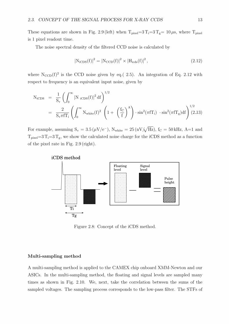
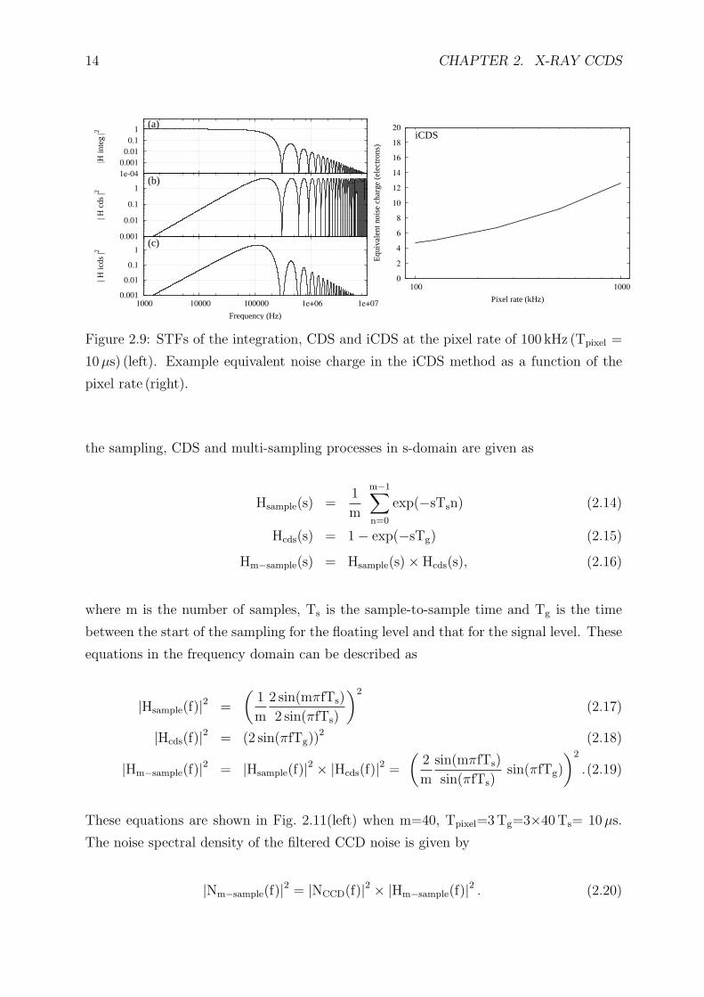
2.3. CONCEPT OF THE SIGNAL PROCESS FOR X-RAY CCDS 13
These equations are shown in Fig. 2.9 (left) when Tpixel=3Ti=3Tg= 10µs, where Tpixel
is 1 pixel readout time.
The noise spectral density of the filtered CCD noise is calculated by
|NiCDS(f)|2 = |NCCD(f)|2 × |Hicds(f)|2 , (2.12)
where NCCD(f)2 is the CCD noise given by eq.( 2.5). An integration of Eq. 2.12 with
respect to frequency is an equivalent input noise, given by
NiCDS =1
Sv
(∫ ∞
0
|N iCDS(f)|2 df
)1/2
=2
SvπfTi
(∫ ∞
0
Nwhite(f)2
(1 +
(fCf
)A)
· sin2(πfTi) · sin2(πfTg)df
)1/2
.(2.13)
For example, assuming Sv = 3.5 (µV/e−), Nwhite = 25 (nV/√
Hz), fC = 50 kHz, A=1 and
Tpixel=3 Ti=3Tg, we show the calculated noise charge for the iCDS method as a function
of the pixel rate in Fig. 2.9 (right).
Pulseheight
Floatinglevel
Signallevel
iCDS method
Ti
Tg
Figure 2.8: Concept of the iCDS method.
Multi-sampling method
A multi-sampling method is applied to the CAMEX chip onboard XMM-Newton and our
ASICs. In the multi-sampling method, the floating and signal levels are sampled many
times as shown in Fig. 2.10. We, next, take the correlation between the sums of the
sampled voltages. The sampling process corresponds to the low-pass filter. The STFs of
14 CHAPTER 2. X-RAY CCDS
0.001
0.01
0.1
1
1000 10000 100000 1e+06 1e+07
| H ic
ds |2
Frequency (Hz)
(c) 0.001
0.01
0.1
1
| H c
ds |2
(b) 1e-04
0.001
0.01
0.1
1
|H in
teg
|2
(a)
0
2
4
6
8
10
12
14
16
18
20
100 1000
Equ
ival
ent n
oise
cha
rge
(ele
ctro
ns)
Pixel rate (kHz)
iCDS
Figure 2.9: STFs of the integration, CDS and iCDS at the pixel rate of 100 kHz (Tpixel =
10µs) (left). Example equivalent noise charge in the iCDS method as a function of the
pixel rate (right).
the sampling, CDS and multi-sampling processes in s-domain are given as
Hsample(s) =1
m
m−1∑n=0
exp(−sTsn) (2.14)
Hcds(s) = 1 − exp(−sTg) (2.15)
Hm−sample(s) = Hsample(s) × Hcds(s), (2.16)
where m is the number of samples, Ts is the sample-to-sample time and Tg is the time
between the start of the sampling for the floating level and that for the signal level. These
equations in the frequency domain can be described as
|Hsample(f)|2 =
(1
m
2 sin(mπfTs)
2 sin(πfTs)
)2
(2.17)
|Hcds(f)|2 = (2 sin(πfTg))2 (2.18)
|Hm−sample(f)|2 = |Hsample(f)|2 × |Hcds(f)|2 =
(2
m
sin(mπfTs)
sin(πfTs)sin(πfTg)
)2
.(2.19)
These equations are shown in Fig. 2.11(left) when m=40, Tpixel=3Tg=3×40Ts= 10µs.
The noise spectral density of the filtered CCD noise is given by
|Nm−sample(f)|2 = |NCCD(f)|2 × |Hm−sample(f)|2 . (2.20)
2.3. CONCEPT OF THE SIGNAL PROCESS FOR X-RAY CCDS 15
We can write an equivalent noise charge in the multi-sampling method by
Nm−sample =1
Sv
(∫ ∞
0
|N m−sample(f)|2 df
)1/2
=2
m Sv
(∫ ∞
0
Nwhite(f)2
(1 +
(fCf
)A)
sin2(mπfTs)
sin2(πfTs)sin2(πfTg)df
)1/2
.(2.21)
For example, assuming Sv = 3.5 (µV/e−), Nwhite = 25 (nV/√
Hz), fC = 50 kHz, A=1,
m=40, Tpixel = 3Tg = 3×40Ts, we show the calculated noise charge for a 40th-sample
method as a function of the pixel rate in Fig. 2.11 (right).
Pulseheight
Floatinglevel
Signallevel
Multi-sampling method
~
~
~
~
~
Ts
Tg
Figure 2.10: Concept of the multi-sampling method.
Comparison between the iCDS method and the multi-sampling method
Based on Figs 2.9 and 2.11, we can see that the performance of the multi-sampling
method is comparable to that of the iCDS method. In the case of the iCDS method,
we need a relatively large resistance of ∼MΩ or capacitance of ∼100 pF to match a
time constant (R×C) of ∼µs for the integrator. The typical integration time is ∼5µs,
and the gain of the integrator is constrained up to 5 from the dynamic range of the
following ADC. A resistor using poly silicon in the TSMC 0.35µm CMOS process is
40 Ω/¤ (¤ stands for 0.35µm2). A poly-insulator-poly (PIP) capacitor in the same process
is 0.89 fF/µm2. When using R=1MΩ and C=1pF, the resistor size of 1MΩ is 55µm2.
When using R=10 kΩ and C=100 pF, the capacitor size of 100 pF becomes 350µm2. The
large resistance and capacitance in ASICs require a large area, which prevents us from
equipping many channels in small area.
A multi-sampling method, however, can easily realize by utilizing a small capacitance
of ∼pF. The gain of the multi-sampling circuit is determined by the number of sample
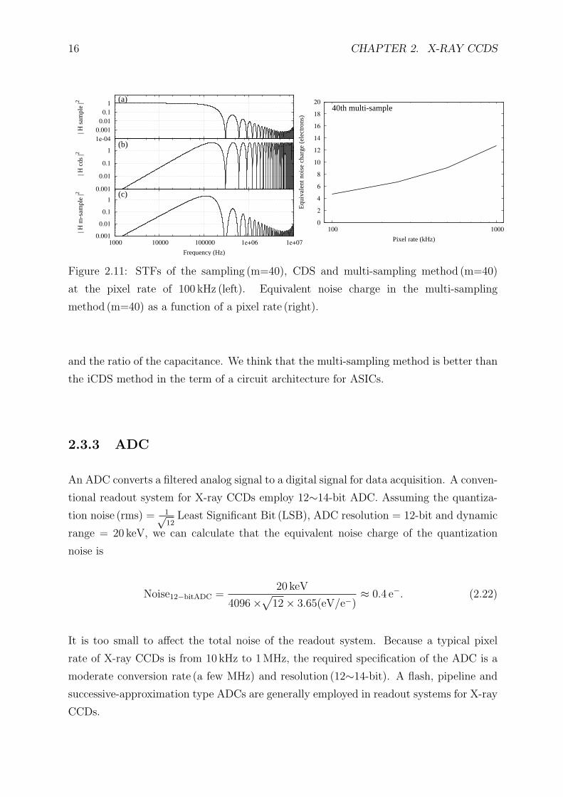
16 CHAPTER 2. X-RAY CCDS
0.001
0.01
0.1
1
1000 10000 100000 1e+06 1e+07
| H m
-sam
ple
|2
Frequency (Hz)
(c) 0.001
0.01
0.1
1
| H c
ds |2
(b) 1e-04
0.001
0.01
0.1
1
| H s
ampl
e |2 (a)
0
2
4
6
8
10
12
14
16
18
20
100 1000
Equ
ival
ent n
oise
cha
rge
(ele
ctro
ns)
Pixel rate (kHz)
40th multi-sample
Figure 2.11: STFs of the sampling (m=40), CDS and multi-sampling method (m=40)
at the pixel rate of 100 kHz (left). Equivalent noise charge in the multi-sampling
method (m=40) as a function of a pixel rate (right).
and the ratio of the capacitance. We think that the multi-sampling method is better than
the iCDS method in the term of a circuit architecture for ASICs.
2.3.3 ADC
An ADC converts a filtered analog signal to a digital signal for data acquisition. A conven-
tional readout system for X-ray CCDs employ 12∼14-bit ADC. Assuming the quantiza-
tion noise (rms) = 1√12
Least Significant Bit (LSB), ADC resolution = 12-bit and dynamic
range = 20 keV, we can calculate that the equivalent noise charge of the quantization
noise is
Noise12−bitADC =20 keV
4096 ×√
12 × 3.65(eV/e−)≈ 0.4 e−. (2.22)
It is too small to affect the total noise of the readout system. Because a typical pixel
rate of X-ray CCDs is from 10 kHz to 1 MHz, the required specification of the ADC is a
moderate conversion rate (a few MHz) and resolution (12∼14-bit). A flash, pipeline and
successive-approximation type ADCs are generally employed in readout systems for X-ray
CCDs.
2.4. ENERGY RESOLUTION 17
2.4 Energy resolution
Energy resolution in FWHM is generally applied to exhibit a spectroscopic capability
for X-ray detectors. The theoretical energy resolution (eV) of CCDs (other Si detectors)
including noise is described as
FWHM = 2.35 × 3.65(eV/e−)
√F
EX(eV)
3.65(eV/e−)+ σ(e−)2 (2.23)
where F is the Fano factor of Si, and σ is the equivalent noise charge derived from the
readout noise, dark noise, transfer noise and so on. The readout noise is generated by
the FDA and by the front-end electronics. The dark noise derived from carriers that are
thermally generated. We can suppress the dark noise by cooling devices. The transfer
noise (spurious charge) is caused by charges generated by impact ionization when transfer
signals are clocked into inversion. This noise is reduced with decreasing the voltage swing
of the clocks and with slowing the voltage change of the clock signals. (Janesick 2001)
illustrates about these noises in detail. The measured energy resolution is better than the
statistical value assuming a Poisson process because a part of an incident photon energy
is expended by non-electron-hole processes (e.g., thermal). The Fano factor is utilized
to compensate the difference between the statistical value and the measured value. We
employed the Fano factor of 0.115 shown in (Janesick 2001) in this paper. The theoretical
limit of energy resolution at 5.9 keV, Manganese (Mn) Kα, by using silicon detectors is
given as
FWHM at 5.9 keV = 2.35 × 3.65(eV/e−)
√0.115
5900(eV)
3.65(eV/e−)
= 117 eV, (2.24)
which we call the Fano limit.

Chapter 3
ASICs
3.1 Overview of ASICs
We have been developing ASICs for X-ray CCD use. They contain four analog channels
each of which consists of preamplifier, band-pass filter and ADC. Therefore, they receive
analog inputs and send digital outputs. Since the ASIC is quite small, it can be placed
very near the X-ray CCD output node so that we can reduce the length of the analog line
to reduce the external noise. With taking into account the performance required and the
maximum CCD output range of 40mV , we set our goal of equivalent input noise level to
be 30µV at 100 kHz pixel rate. We also expect it to function properly up to 1MHz. Our
ASIC project will enable anyone to easily construct the CCD camera system with very
low noise and high pixel rate, which eliminates difficulties of tuning the analog electronics.
We have developed 4 types of ASICs that are named as Matsuura-Doty (MD01),
Matsuura-Nakajima-Doty (MND01), MD02 and MND02. They are divided into 2 groups:
one, a first group, contains MD01, MND01 and MD02 while the other contains MND02.
MD01, the first ASIC developed in our series, properly functions as we designed, but there
are some problems. They are the malfunction of LVDS circuit and the low maximum pixel
rate as explained in Chap. 4. We designed the second ASIC, MND01, in order to solve
these problems. We confirmed that they are properly solved, however, we encountered
another problem that caused the degradation of INL and signal-to-noise ratio. The third
ASIC developed, MD02, cleared these problems. Based on ASIC developments of the
first group, we reached the ASIC, MND02, in which we reduced the noise figure of the
preamplifier by 50% and improved the speed of LVDS receiver.
The circuit architectures of these ASIC are almost the same that will be briefly ex-
plained here. One ASIC chip has four readout channels as shown in Fig. 3.1. One readout
channel consists of a preamplifier, 5-bit digital-to-analog converter (DAC) and two ∆Σ
19
20 CHAPTER 3. ASICS
DAC
ADC
ADC
ASICX-ray CCDsignal (1 pixel)
001101011010110001101010001001000100011010001001000100010100100001........
each modulatoroutput (1 pixel)
155-bit stream
(2 V(n) −1) h(n)
= −h(1) −h(2) +h(3)...Σ
V(n) : n-th outputh(n) : filter coefficient
decimation filter
decimal value
signallevel
floatinglevel
voltage difference
amp
Figure 3.1: Data flow diagram of the readout system employing our ASIC.
ADCs that we call an odd ADC and an even ADC. The CCD signals are fed into ASIC
through capacitors to remove DC component and converted from analog signals to digital
bit-streams. Since the digital bit-streams are produced from the ∆Σ ADC, they have to
be converted to the decimal values through the decimation filter. The following digital
processor (DP) performs data acquisition and the decimation process.
The conventional circuit configuration for the readout of CCD signals consists of a
preamplifier, band-pass filter and ADC as shown in Fig. 2.7. In the case of our ASICs, the
∆Σ ADCs function as the band-pass filter as well as ADC, so that the circuit configuration
can be relatively simple compared with the ordinary readout systems.
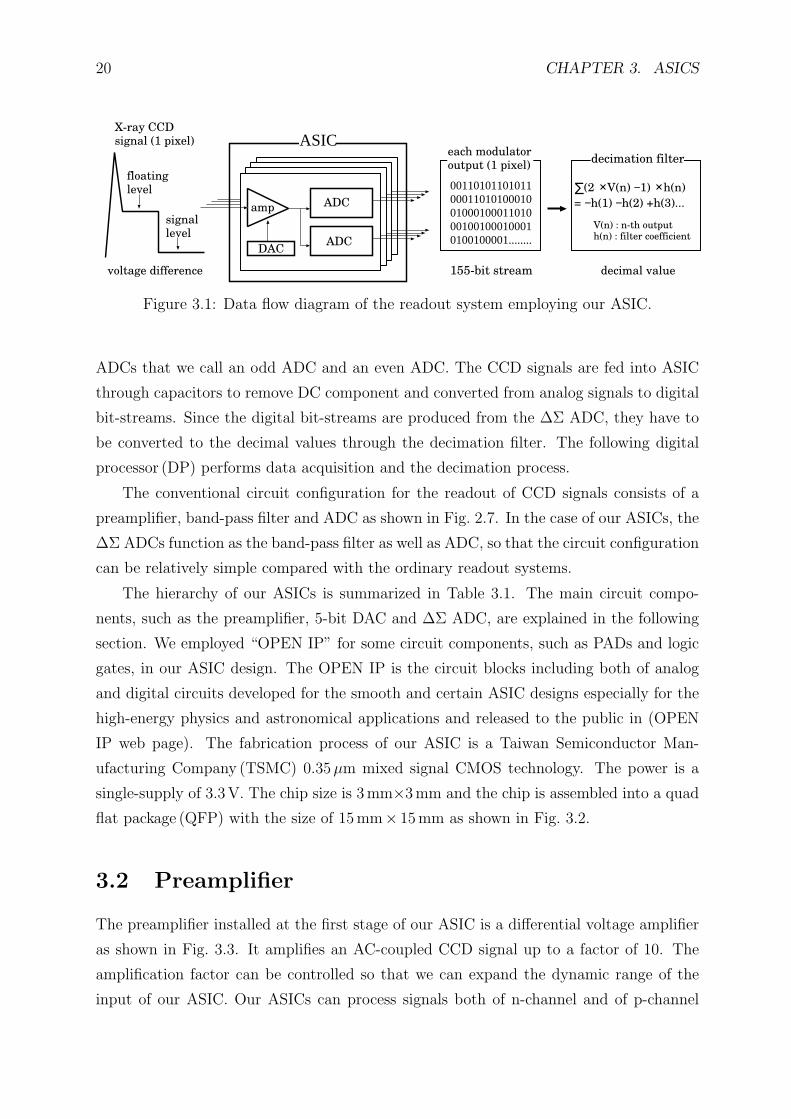
The hierarchy of our ASICs is summarized in Table 3.1. The main circuit compo-
nents, such as the preamplifier, 5-bit DAC and ∆Σ ADC, are explained in the following
section. We employed “OPEN IP” for some circuit components, such as PADs and logic
gates, in our ASIC design. The OPEN IP is the circuit blocks including both of analog
and digital circuits developed for the smooth and certain ASIC designs especially for the
high-energy physics and astronomical applications and released to the public in (OPEN
IP web page). The fabrication process of our ASIC is a Taiwan Semiconductor Man-
ufacturing Company (TSMC) 0.35µm mixed signal CMOS technology. The power is a
single-supply of 3.3 V. The chip size is 3 mm×3mm and the chip is assembled into a quad
flat package (QFP) with the size of 15 mm× 15mm as shown in Fig. 3.2.
3.2 Preamplifier
The preamplifier installed at the first stage of our ASIC is a differential voltage amplifier
as shown in Fig. 3.3. It amplifies an AC-coupled CCD signal up to a factor of 10. The
amplification factor can be controlled so that we can expand the dynamic range of the
input of our ASIC. Our ASICs can process signals both of n-channel and of p-channel
3.2. PREAMPLIFIER 21
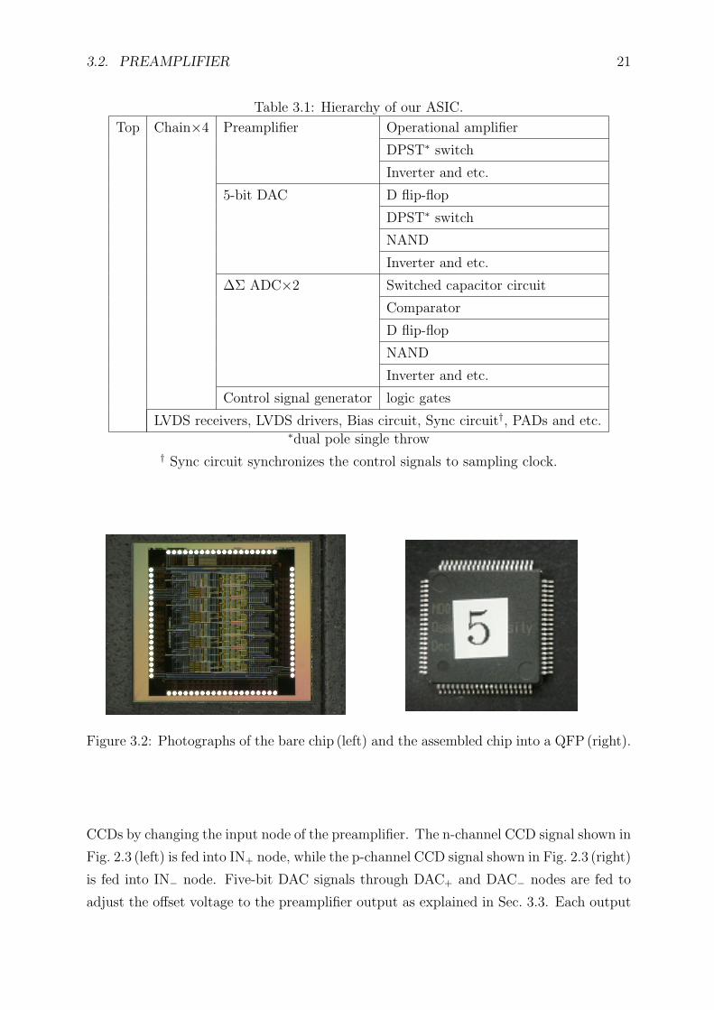
Table 3.1: Hierarchy of our ASIC.
Top Chain×4 Preamplifier Operational amplifier
DPST∗ switch
Inverter and etc.
5-bit DAC D flip-flop
DPST∗ switch
NAND
Inverter and etc.
∆Σ ADC×2 Switched capacitor circuit
Comparator
D flip-flop
NAND
Inverter and etc.
Control signal generator logic gates
LVDS receivers, LVDS drivers, Bias circuit, Sync circuit†, PADs and etc.∗dual pole single throw
† Sync circuit synchronizes the control signals to sampling clock.
Figure 3.2: Photographs of the bare chip (left) and the assembled chip into a QFP (right).
CCDs by changing the input node of the preamplifier. The n-channel CCD signal shown in
Fig. 2.3 (left) is fed into IN+ node, while the p-channel CCD signal shown in Fig. 2.3 (right)
is fed into IN− node. Five-bit DAC signals through DAC+ and DAC− nodes are fed to
adjust the offset voltage to the preamplifier output as explained in Sec. 3.3. Each output
22 CHAPTER 3. ASICS
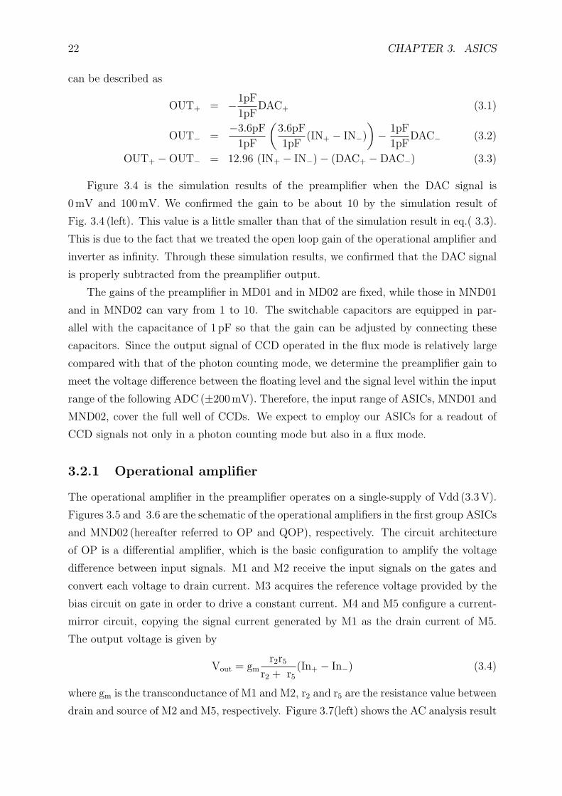
can be described as
OUT+ = −1pF
1pFDAC+ (3.1)
OUT− =−3.6pF
1pF
(3.6pF
1pF(IN+ − IN−)
)− 1pF
1pFDAC− (3.2)
OUT+ − OUT− = 12.96 (IN+ − IN−) − (DAC+ − DAC−) (3.3)
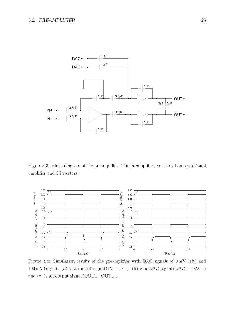
Figure 3.4 is the simulation results of the preamplifier when the DAC signal is
0 mV and 100mV. We confirmed the gain to be about 10 by the simulation result of
Fig. 3.4 (left). This value is a little smaller than that of the simulation result in eq.( 3.3).
This is due to the fact that we treated the open loop gain of the operational amplifier and
inverter as infinity. Through these simulation results, we confirmed that the DAC signal
is properly subtracted from the preamplifier output.
The gains of the preamplifier in MD01 and in MD02 are fixed, while those in MND01
and in MND02 can vary from 1 to 10. The switchable capacitors are equipped in par-
allel with the capacitance of 1 pF so that the gain can be adjusted by connecting these
capacitors. Since the output signal of CCD operated in the flux mode is relatively large
compared with that of the photon counting mode, we determine the preamplifier gain to
meet the voltage difference between the floating level and the signal level within the input
range of the following ADC (±200mV). Therefore, the input range of ASICs, MND01 and
MND02, cover the full well of CCDs. We expect to employ our ASICs for a readout of
CCD signals not only in a photon counting mode but also in a flux mode.
3.2.1 Operational amplifier
The operational amplifier in the preamplifier operates on a single-supply of Vdd (3.3V).
Figures 3.5 and 3.6 are the schematic of the operational amplifiers in the first group ASICs
and MND02 (hereafter referred to OP and QOP), respectively. The circuit architecture
of OP is a differential amplifier, which is the basic configuration to amplify the voltage
difference between input signals. M1 and M2 receive the input signals on the gates and
convert each voltage to drain current. M3 acquires the reference voltage provided by the
bias circuit on gate in order to drive a constant current. M4 and M5 configure a current-
mirror circuit, copying the signal current generated by M1 as the drain current of M5.
The output voltage is given by
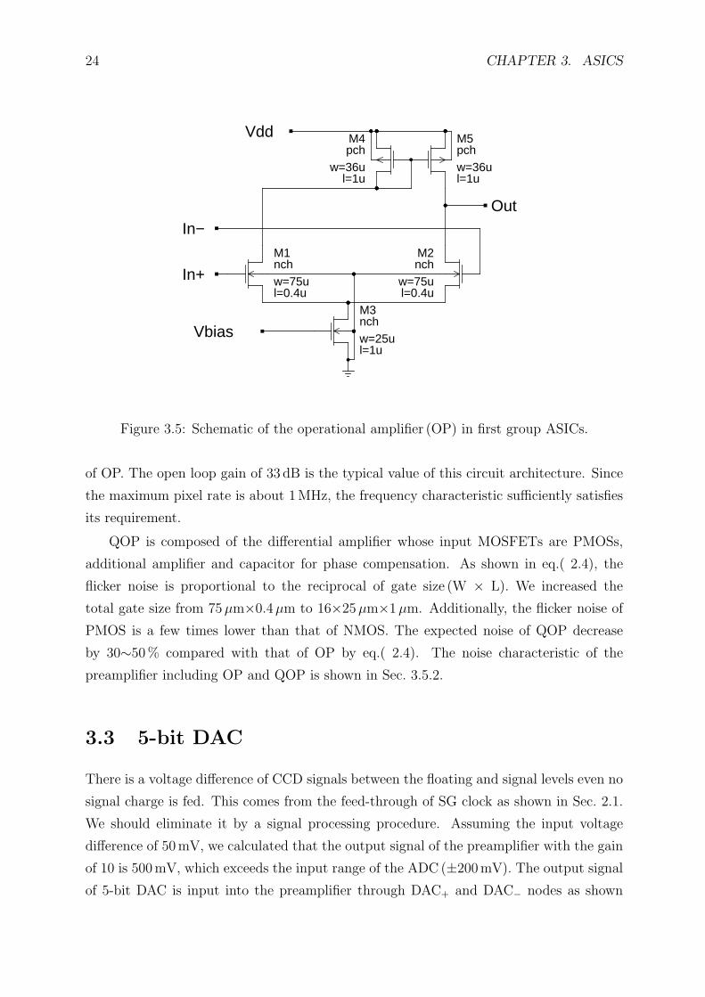
Vout = gmr2r5
r2 + r5
(In+ − In−) (3.4)
where gm is the transconductance of M1 and M2, r2 and r5 are the resistance value between
drain and source of M2 and M5, respectively. Figure 3.7(left) shows the AC analysis result
3.2. PREAMPLIFIER 23
IN+
IN−
OUT+
OUT−
DAC−
DAC+
3.6pF
3.6pF
3.6pF
3.6pF
1pF
1pF
1pF
1pF
1pF
1pF
2pF 2pF
Figure 3.3: Block diagram of the preamplifier. The preamplifier consists of an operational
amplifier and 2 inverters.
-0.1
0
0.1
0.2
0.3
0 0.5 1 1.5 2
OU
T+
- O
UT
- (V
)
Time (us)
(c)
0
0.1
0.2
DA
C+
- D
AC
- (V
)
(b)-0.01
0
0.01
0.02
0.03
IN+
- I
N-
(V) (a)
-0.1
0
0.1
0.2
0.3
0 0.5 1 1.5 2
OU
T+
- O
UT
- (V
)
Time (us)
(c)
0
0.1
0.2
DA
C+
- D
AC
- (V
)
(b)-0.01
0
0.01
0.02
0.03
IN+
- I
N-
(V) (a)
Figure 3.4: Simulation results of the preamplifier with DAC signals of 0mV (left) and
100mV (right). (a) is an input signal (IN+−IN−), (b) is a DAC signal (DAC+−DAC−)
and (c) is an output signal (OUT+−OUT−).
24 CHAPTER 3. ASICS
Vdd
In−
In+
Vbias
Out
M5pchw=36ul=1u
M4pch
w=36ul=1u
M1nchw=75ul=0.4u
M2nch
w=75ul=0.4u
M3nchw=25ul=1u
Figure 3.5: Schematic of the operational amplifier (OP) in first group ASICs.
of OP. The open loop gain of 33 dB is the typical value of this circuit architecture. Since
the maximum pixel rate is about 1MHz, the frequency characteristic sufficiently satisfies
its requirement.
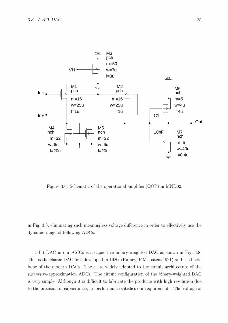
QOP is composed of the differential amplifier whose input MOSFETs are PMOSs,
additional amplifier and capacitor for phase compensation. As shown in eq.( 2.4), the
flicker noise is proportional to the reciprocal of gate size (W × L). We increased the
total gate size from 75µm×0.4µm to 16×25µm×1µm. Additionally, the flicker noise of
PMOS is a few times lower than that of NMOS. The expected noise of QOP decrease
by 30∼50% compared with that of OP by eq.( 2.4). The noise characteristic of the
preamplifier including OP and QOP is shown in Sec. 3.5.2.
3.3 5-bit DAC
There is a voltage difference of CCD signals between the floating and signal levels even no
signal charge is fed. This comes from the feed-through of SG clock as shown in Sec. 2.1.
We should eliminate it by a signal processing procedure. Assuming the input voltage
difference of 50mV, we calculated that the output signal of the preamplifier with the gain
of 10 is 500mV, which exceeds the input range of the ADC (±200mV). The output signal
of 5-bit DAC is input into the preamplifier through DAC+ and DAC− nodes as shown
3.3. 5-BIT DAC 25
In+
M5nch
w=6ul=20u
m=32
M1pch
w=25ul=1u
m=16
M4nch
w=6ul=20u
m=32
M2pch
w=25ul=1u
m=16
Vdd
Vdd M3pch
w=3ul=3u
m=50VH
M6pch
w=4ul=4u
m=5
M7nch
w=40ul=0.4u
m=5
Out
Vdd
C1
10pF
In−
Figure 3.6: Schematic of the operational amplifier (QOP) in MND02.
in Fig. 3.3, eliminating such meaningless voltage difference in order to effectively use the
dynamic range of following ADCs.
5-bit DAC in our ASICs is a capacitive binary-weighted DAC as shown in Fig. 3.8.
This is the classic DAC first developed in 1920s (Rainey, P.M. patent 1921) and the back-
bone of the modern DACs. These are widely adapted to the circuit architecture of the
successive-approximation ADCs. The circuit configuration of the binary-weighted DAC
is very simple. Although it is difficult to fabricate the products with high resolution due
to the precision of capacitance, its performance satisfies our requirements. The voltage of
26 CHAPTER 3. ASICS
-160
-110
-60
-10
40
90
140
190
1 100 10000 1e+06 1e+08 1e+10
Vol
tage
Pha
se (
deg)
Frequency (Hz)
(b)
-20
0
20
40
60
80
100
Vol
tage
Mag
nitu
de (
dB)
(b)
(a)OP
-160
-110
-60
-10
40
90
140
190
1 100 10000 1e+06 1e+08 1e+10
Vol
tage
Pha
se (
deg)
Frequency (Hz)
(b)
-20
0
20
40
60
80
100
Vol
tage
Mag
nitu
de (
dB)
(b)
(a)QOP
Figure 3.7: AC analysis results of the operational amplifiers (OP : left) and (QOP : right).
(a) and (b) show the voltage magnitude and the voltage phase as a function of frequency,
respectively.
each output is given by
DAC+ =(480 fF × V1) + (240 fF × V2) + (120 fF × V3)
1 pF
+(60 fF × V4) + (30 fF × V5) + (30 fF × VREF−)
1 pF
(3.5)
DAC− =(960 fF × VREF−)
1 pF(3.6)
where V1, V2, V3, V4 and V5 are the reference voltage for the capacitance string shown
in Fig. 3.8. These voltage levels are determined to whether VREF+ (1.2V+COM) or
VREF− (COM), where COM is the operating point voltage of the inverters. The DAC
output can be finally described as
DAC+ − DAC− ∼ Din
32× 1.2 V (3.7)
where Din is the binary code loaded to the DAC register shown in Fig. 3.8. The DAC
registers of 4 channels are cascaded so that we can set the DAC by only one data line (Din).
Figure 3.9 (top) shows the format for Din of MD01 and MD02 which contains the 4 DAC
codes of D4∼D0 for channel-3, C4∼C0 for channel-2, B4∼B0 for channel-1 and A4∼A0
for channel-0. In the case of MND01 and MND02, the register has both codes for the
adjust of the preamplifier gain (Dp, Cp, Bp and Ap) and DAC (Dd, Cd, Bd and Ad)
as shown in Fig 3.9 (bottom). Dclk is a serial clock to transfer Din into the serial shift
register on the rising edge. Dload is a control input signal to latch the contents of the
3.3. 5-BIT DAC 27
1pF
1pF
DAC+
DAC−
C1
480fF
C2
240fF
C3
120fF
C4
60fF
C5
30fF
S1 S2 S3 S4 S5
VREF+
C6
30fF
C7
960fF
VREF−
Dload
Denb
Register
DinDclk
Dout
Figure 3.8: Block diagram of 5-bit DAC.
shift resister on the rising edge of Dclk. Denb is a control input signal to power on the
switches in the register, generating the setup voltage during the active level. Dout is the
serial data out of Din through the register. The Dout of channel-0 is connected to the Din
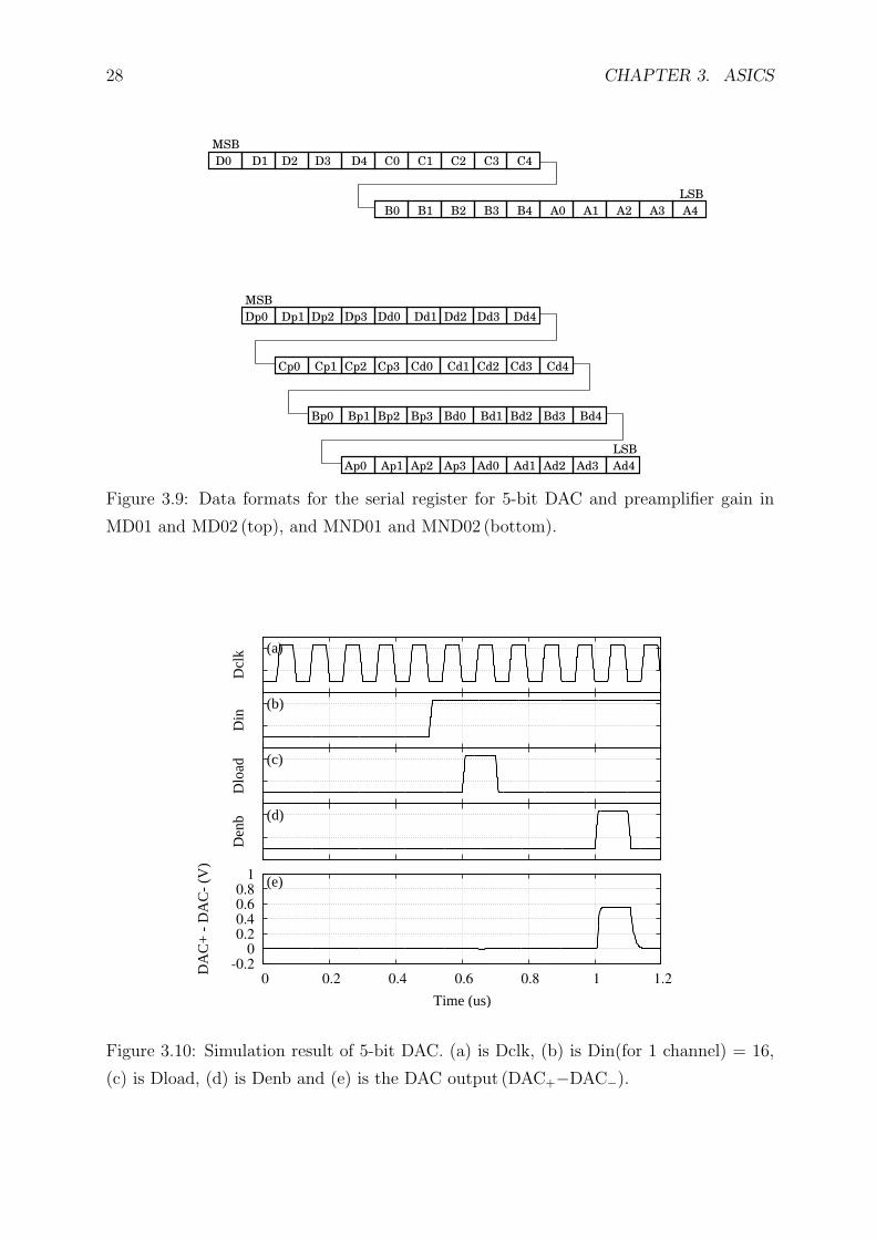
of channel-1 and the Dout of channel-3 is finally transferred outside an ASIC. Figure 3.10
shows the simulation result of 5-bit DAC with Din (for 1 channel) = 16. The output
voltage obtained by this simulation is 550mV, which is comparable to the expected value
of 600 mV from eq.( 3.7).
28 CHAPTER 3. ASICS
D3D2D1D0 D4 C0 C1 C2 C3 C4
B0 B1 B2 B3 B4 A0 A1 A2 A3 A4
MSB
LSB
Dd3Dd2Dd1Dd0 Dd4
MSB
LSB
Dp3Dp2Dp1Dp0
Cd3Cd2Cd1Cd0 Cd4Cp3Cp2Cp1Cp0
Bd3Bd2Bd1Bd0 Bd4Bp3Bp2Bp1Bp0
Ad3Ad2Ad1Ad0 Ad4Ap3Ap2Ap1Ap0
Figure 3.9: Data formats for the serial register for 5-bit DAC and preamplifier gain in
MD01 and MD02 (top), and MND01 and MND02 (bottom).
-0.2
0
0.2
0.4
0.6
0.8
1
0 0.2 0.4 0.6 0.8 1 1.2
DA
C+
- D
AC
- (V
)
Time (us)
(e)
Den
b (d)
Dlo
ad (c)
Din
(b)
Dcl
k (a)
Figure 3.10: Simulation result of 5-bit DAC. (a) is Dclk, (b) is Din(for 1 channel) = 16,
(c) is Dload, (d) is Denb and (e) is the DAC output (DAC+−DAC−).
3.4. ∆Σ ADC 29
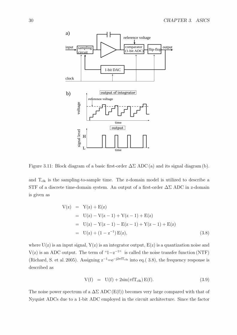
3.4 ∆Σ ADC
In general, there are two types of ADCs, a Nyquist-rate converter and an oversampled
converter. The Nyquist-rate converters, such as flash ADC, slope ADC and cyclic ADC,
perform Analog to Digital conversion by using a single sampled analog signal. The over-
sampled converters utilize a sequential data sampling at high frequency compared with
that of the input signal. A decimal output of the oversampled ADC is obtained by the
decimation process for noise and sample rate reduction.
We employed the oversampled converter, ∆Σ ADC, because this type of ADC
• can achieve a high resolution at a moderately short conversion time.
• does not need accurate circuit components.
• can be fabricated by a low cost CMOS process.
• functions not only as an ADC but also a band-pass filter.
The differential averaging function can be implemented in ∆Σ ADC as explained in
Sec. 3.4.2, which is not automatically in Nyquist-rate converters. The ∆Σ ADC en-
ables us to remove a band-pass circuits from the readout system and simplify the circuit
configuration.
3.4.1 Concept of ∆Σ ADCs
Fig. 3.11 shows an example block diagram of a first-order ∆Σ ADC(a) and its signal
diagram (b). The ADC consists of a sampling circuit (a switched-capacitor circuit), inte-
grator, comparator (1-bit ADC), flip-flop and 1-bit DAC. The number of cascading pairs
of sampling circuit and integrator represents the order of ∆Σ ADC. The sampling circuit
outputs the charges to the integrator, the amount of which is proportional to the input
voltage. The comparator followed by the D flip-flop compares the output of the integra-
tor with a reference voltage and outputs the clocked bitstream. When the output of the
integrator is higher than the reference voltage, the logic level of the output bit becomes
high. The 1-bit DAC, subsequently, subtracts the reference charges from the integrator
to regulate the output voltage of the integrator. Therefore, the frequency of high level
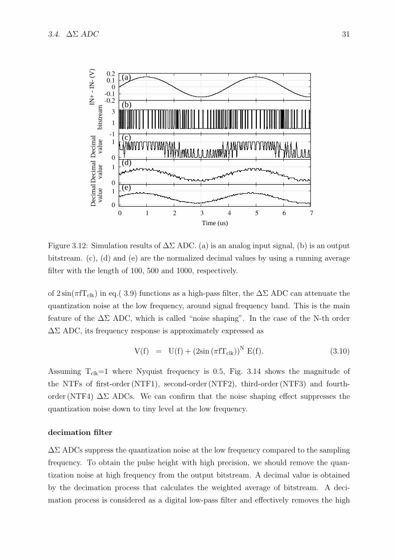
in the output bitstream increases as the input signal gets larger. Figure 3.12 shows the
simulation results of the ∆Σ ADC. The density of high level in the output bitstream in
Fig.(b) is changing with the input signal voltage in Fig.(a).
noise shaping
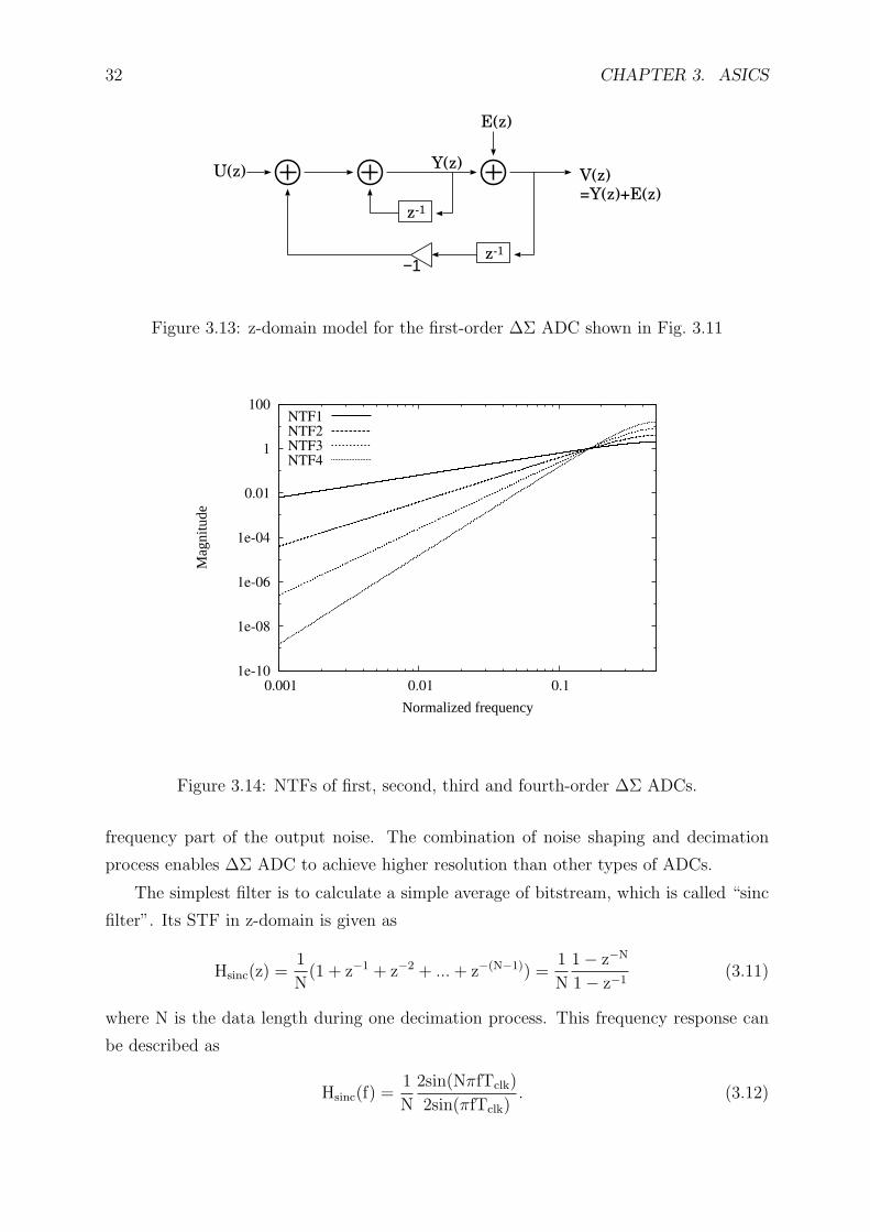
Figure 3.13 shows the z-domain model of the first-order ∆Σ ADC shown in Fig. 3.11(a).
The parameter ”z” represents ”esTclk=ej2πfTclk”, where j is imaginary unit, f is frequency
30 CHAPTER 3. ASICS
sampling circuit
comparator(1-bit ADC)
1-bit DAC
input output
clock
output of integrator
output
L
H
volt
age
time
time
reference voltage
reference voltage
sign
al le
vel
b)
a)
flip-flop
Figure 3.11: Block diagram of a basic first-order ∆Σ ADC(a) and its signal diagram (b).
and Tclk is the sampling-to-sample time. The z-domain model is utilized to describe a
STF of a discrete time-domain system. An output of a first-order ∆Σ ADC in z-domain
is given as
V(z) = Y(z) + E(z)
= U(z) − V(z − 1) + Y(z − 1) + E(z)
= U(z) − Y(z − 1) − E(z − 1) + Y(z − 1) + E(z)
= U(z) + (1 − z−1) E(z), (3.8)
where U(z) is an input signal, Y(z) is an integrator output, E(z) is a quantization noise and
V(z) is an ADC output. The term of “1−z−1” is called the noise transfer function (NTF)
(Richard, S. et al. 2005). Assigning z−1=e−j2πfTclk into eq.( 3.8), the frequency response is
described as
V(f) = U(f) + 2sin(πfTclk) E(f). (3.9)
The noise power spectrum of a ∆Σ ADC(E(f)) becomes very large compared with that of
Nyquist ADCs due to a 1-bit ADC employed in the circuit architecture. Since the factor
3.4. ∆Σ ADC 31
0
1
0 1 2 3 4 5 6 7
Dec
imal
valu
e
Time (us)
(e) 0
1
Dec
imal
valu
e (d) 0
1
Dec
imal
valu
e (c)-1
1
3
bits
trea
m (b)-0.2
-0.1
0
0.1
0.2
IN+
- I
N-
(V)
(a)
Figure 3.12: Simulation results of ∆Σ ADC. (a) is an analog input signal, (b) is an output
bitstream. (c), (d) and (e) are the normalized decimal values by using a running average
filter with the length of 100, 500 and 1000, respectively.
of 2 sin(πfTclk) in eq.( 3.9) functions as a high-pass filter, the ∆Σ ADC can attenuate the
quantization noise at the low frequency, around signal frequency band. This is the main
feature of the ∆Σ ADC, which is called “noise shaping”. In the case of the N-th order
∆Σ ADC, its frequency response is approximately expressed as
V(f) = U(f) + (2sin (πfTclk))N E(f). (3.10)
Assuming Tclk=1 where Nyquist frequency is 0.5, Fig. 3.14 shows the magnitude of
the NTFs of first-order (NTF1), second-order (NTF2), third-order (NTF3) and fourth-
order (NTF4) ∆Σ ADCs. We can confirm that the noise shaping effect suppresses the
quantization noise down to tiny level at the low frequency.
decimation filter
∆Σ ADCs suppress the quantization noise at the low frequency compared to the sampling
frequency. To obtain the pulse height with high precision, we should remove the quan-
tization noise at high frequency from the output bitstream. A decimal value is obtained
by the decimation process that calculates the weighted average of bitstream. A deci-
mation process is considered as a digital low-pass filter and effectively removes the high
32 CHAPTER 3. ASICS
z-1
z-1
U(z)
E(z)
V(z)
=Y(z)+E(z)
Y(z)
−1
Figure 3.13: z-domain model for the first-order ∆Σ ADC shown in Fig. 3.11
1e-10
1e-08
1e-06
1e-04
0.01
1
100
0.001 0.01 0.1
Mag
nitu
de
Normalized frequency
12bit ADC
NTF1
NTF2
NTF3
NTF4
Figure 3.14: NTFs of first, second, third and fourth-order ∆Σ ADCs.
frequency part of the output noise. The combination of noise shaping and decimation
process enables ∆Σ ADC to achieve higher resolution than other types of ADCs.
The simplest filter is to calculate a simple average of bitstream, which is called “sinc
filter”. Its STF in z-domain is given as
Hsinc(z) =1
N(1 + z−1 + z−2 + ... + z−(N−1)) =
1
N
1 − z−N
1 − z−1(3.11)
where N is the data length during one decimation process. This frequency response can
be described as
Hsinc(f) =1
N
2sin(NπfTclk)
2sin(πfTclk). (3.12)
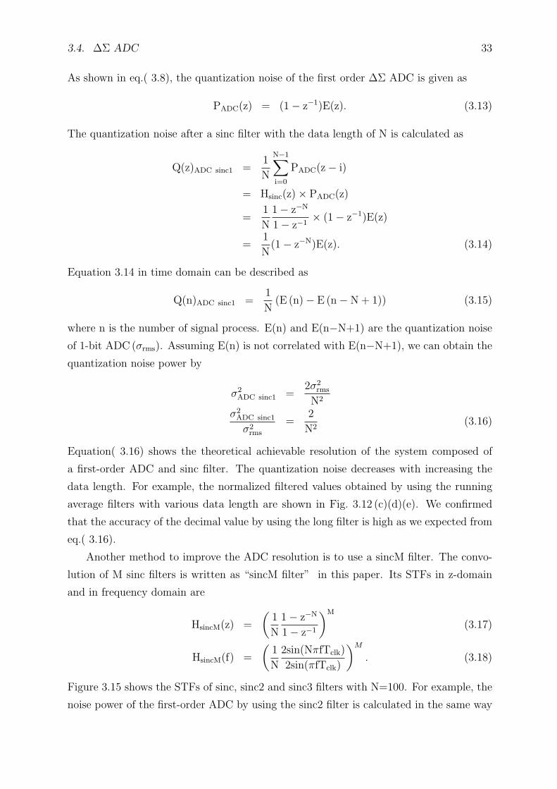
3.4. ∆Σ ADC 33
As shown in eq.( 3.8), the quantization noise of the first order ∆Σ ADC is given as
PADC(z) = (1 − z−1)E(z). (3.13)
The quantization noise after a sinc filter with the data length of N is calculated as
Q(z)ADC sinc1 =1
N
N−1∑i=0
PADC(z − i)
= Hsinc(z) × PADC(z)
=1
N
1 − z−N
1 − z−1× (1 − z−1)E(z)
=1
N(1 − z−N)E(z). (3.14)
Equation 3.14 in time domain can be described as
Q(n)ADC sinc1 =1
N(E (n) − E (n − N + 1)) (3.15)
where n is the number of signal process. E(n) and E(n−N+1) are the quantization noise
of 1-bit ADC (σrms). Assuming E(n) is not correlated with E(n−N+1), we can obtain the
quantization noise power by
σ2ADC sinc1 =
2σ2rms
N2
σ2ADC sinc1
σ2rms
=2
N2(3.16)
Equation( 3.16) shows the theoretical achievable resolution of the system composed of
a first-order ADC and sinc filter. The quantization noise decreases with increasing the
data length. For example, the normalized filtered values obtained by using the running
average filters with various data length are shown in Fig. 3.12 (c)(d)(e). We confirmed
that the accuracy of the decimal value by using the long filter is high as we expected from
eq.( 3.16).
Another method to improve the ADC resolution is to use a sincM filter. The convo-
lution of M sinc filters is written as “sincM filter” in this paper. Its STFs in z-domain
and in frequency domain are
HsincM(z) =
(1
N
1 − z−N
1 − z−1
)M
(3.17)
HsincM(f) =
(1
N
2sin(NπfTclk)
2sin(πfTclk)
)M
. (3.18)
Figure 3.15 shows the STFs of sinc, sinc2 and sinc3 filters with N=100. For example, the
noise power of the first-order ADC by using the sinc2 filter is calculated in the same way
34 CHAPTER 3. ASICS
as eq.( 3.14) ;
Q(z)ADC sinc2 = Hsinc2(z) × PADC(z)
= Hsinc1(z) × Hsinc1(z) × PADC(z)
= Hsinc1(z) ×1
N(1 − z−N)E(z). (3.19)
The factor of Hsinc1(z) means to calculate the average. Equation 3.19 in time domain is
Q(n)ADC sinc2 =1
N
N−1∑i=0
(1
N(E (n − i) − E (n − N + 1 − i))
). (3.20)
The noise of the first-order ADC with sinc2 filter is
σ2ADC sicn2 =
N × 2σ2rms
N4
=2σ2
rms
N3. (3.21)
A sinc2 filter effectively reduces the quantization noise compared with a sinc filter in
eq.( 3.16). A sinc(L+1) filter is generally appropriate for the L-th order ∆Σ ADC (Richard,
S. et al. 2005). The theoretical noise power of the system composed with the L-th order
ADC and sincM filter is given by
σ2ADCL sicnM =
2L
NL+Mσ2
rms. (3.22)
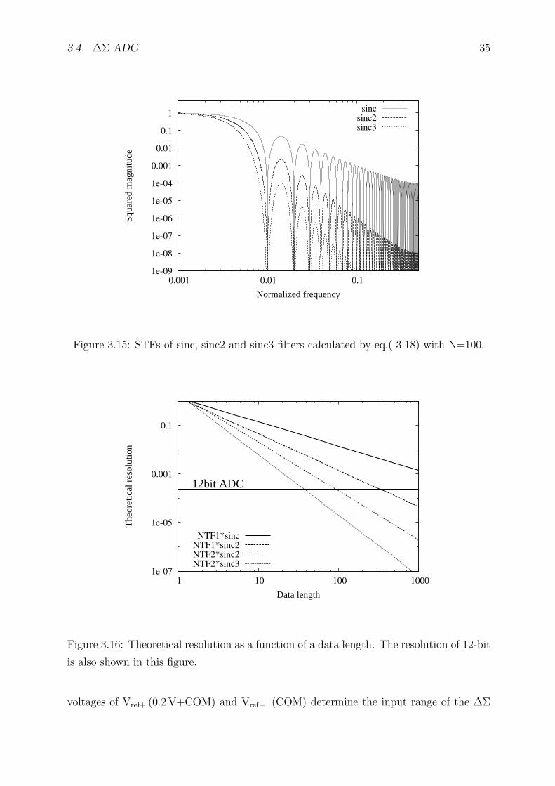
The achievable resolution of a first-order and of a second-order ADC employing several
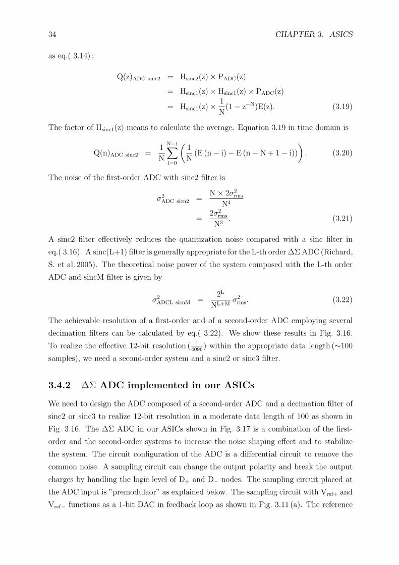
decimation filters can be calculated by eq.( 3.22). We show these results in Fig. 3.16.
To realize the effective 12-bit resolution ( 14096
) within the appropriate data length (∼100
samples), we need a second-order system and a sinc2 or sinc3 filter.
3.4.2 ∆Σ ADC implemented in our ASICs
We need to design the ADC composed of a second-order ADC and a decimation filter of
sinc2 or sinc3 to realize 12-bit resolution in a moderate data length of 100 as shown in
Fig. 3.16. The ∆Σ ADC in our ASICs shown in Fig. 3.17 is a combination of the first-
order and the second-order systems to increase the noise shaping effect and to stabilize
the system. The circuit configuration of the ADC is a differential circuit to remove the
common noise. A sampling circuit can change the output polarity and break the output
charges by handling the logic level of D+ and D− nodes. The sampling circuit placed at
the ADC input is ”premodulaor” as explained below. The sampling circuit with Vref+ and
Vref− functions as a 1-bit DAC in feedback loop as shown in Fig. 3.11 (a). The reference
3.4. ∆Σ ADC 35
1e-09
1e-08
1e-07
1e-06
1e-05
1e-04
0.001
0.01
0.1
1
0.001 0.01 0.1
Squa
red
mag
nitu
de
Normalized frequency
12bit ADC
sinc
sinc2
sinc3
Figure 3.15: STFs of sinc, sinc2 and sinc3 filters calculated by eq.( 3.18) with N=100.
1e-07
1e-05
0.001
0.1
1 10 100 1000
The
oret
ical
res
olut
ion
Data length
12bit ADC
NTF1*sinc
NTF1*sinc2
NTF2*sinc2
NTF2*sinc3
Figure 3.16: Theoretical resolution as a function of a data length. The resolution of 12-bit
is also shown in this figure.
voltages of Vref+ (0.2V+COM) and Vref− (COM) determine the input range of the ∆Σ
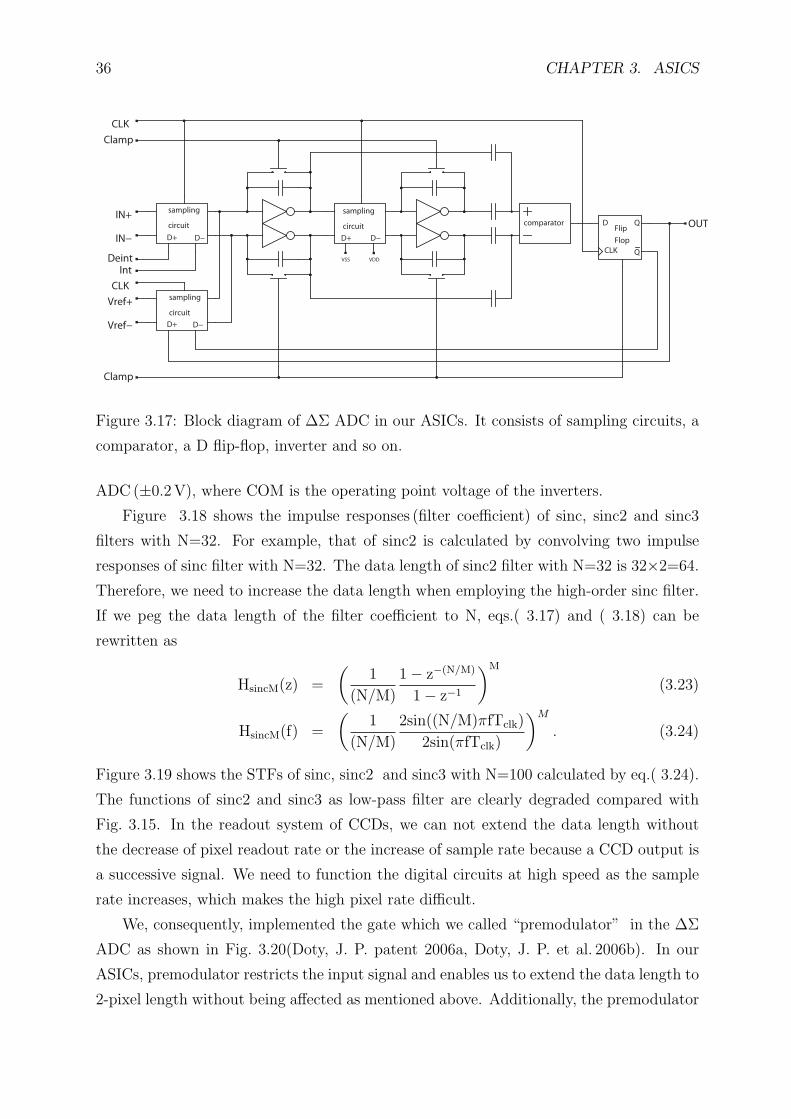
36 CHAPTER 3. ASICS
IN+
IN−
DeintInt
VSS VDD
Vref+
Vref−
OUT
CLK
CLK
D+ D−
comparator
D+ D−
sampling
circuit
D+ D−
Clamp
Clamp
Flip
Flop
D
CLK
Q
Q
sampling
circuit
sampling
circuit
Figure 3.17: Block diagram of ∆Σ ADC in our ASICs. It consists of sampling circuits, a
comparator, a D flip-flop, inverter and so on.
ADC (±0.2V), where COM is the operating point voltage of the inverters.
Figure 3.18 shows the impulse responses (filter coefficient) of sinc, sinc2 and sinc3
filters with N=32. For example, that of sinc2 is calculated by convolving two impulse
responses of sinc filter with N=32. The data length of sinc2 filter with N=32 is 32×2=64.
Therefore, we need to increase the data length when employing the high-order sinc filter.
If we peg the data length of the filter coefficient to N, eqs.( 3.17) and ( 3.18) can be
rewritten as
HsincM(z) =
(1
(N/M)
1 − z−(N/M)
1 − z−1
)M
(3.23)
HsincM(f) =
(1
(N/M)
2sin((N/M)πfTclk)
2sin(πfTclk)
)M
. (3.24)
Figure 3.19 shows the STFs of sinc, sinc2 and sinc3 with N=100 calculated by eq.( 3.24).
The functions of sinc2 and sinc3 as low-pass filter are clearly degraded compared with
Fig. 3.15. In the readout system of CCDs, we can not extend the data length without
the decrease of pixel readout rate or the increase of sample rate because a CCD output is
a successive signal. We need to function the digital circuits at high speed as the sample
rate increases, which makes the high pixel rate difficult.
We, consequently, implemented the gate which we called “premodulator” in the ∆Σ
ADC as shown in Fig. 3.20(Doty, J. P. patent 2006a, Doty, J. P. et al. 2006b). In our
ASICs, premodulator restricts the input signal and enables us to extend the data length to
2-pixel length without being affected as mentioned above. Additionally, the premodulator
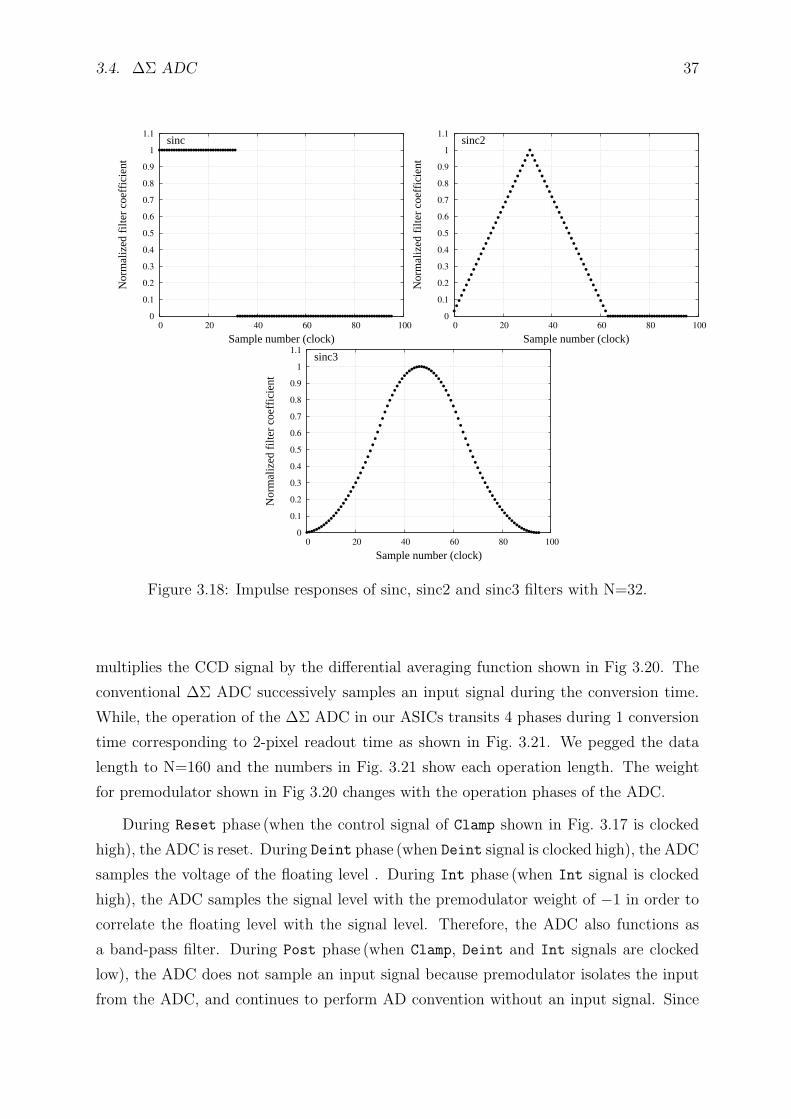
3.4. ∆Σ ADC 37
0
0.1
0.2
0.3
0.4
0.5
0.6
0.7
0.8
0.9
1
1.1
0 20 40 60 80 100
Nor
mal
ized
filt
er c
oeff
icie
nt
Sample number (clock)
sinc
0
0.1
0.2
0.3
0.4
0.5
0.6
0.7
0.8
0.9
1
1.1
0 20 40 60 80 100
Nor
mal
ized
filt
er c
oeff
icie
nt
Sample number (clock)
sinc2
0
0.1
0.2
0.3
0.4
0.5
0.6
0.7
0.8
0.9
1
1.1
0 20 40 60 80 100
Nor
mal
ized
filt
er c
oeff
icie
nt
Sample number (clock)
sinc3
Figure 3.18: Impulse responses of sinc, sinc2 and sinc3 filters with N=32.
multiplies the CCD signal by the differential averaging function shown in Fig 3.20. The
conventional ∆Σ ADC successively samples an input signal during the conversion time.
While, the operation of the ∆Σ ADC in our ASICs transits 4 phases during 1 conversion
time corresponding to 2-pixel readout time as shown in Fig. 3.21. We pegged the data
length to N=160 and the numbers in Fig. 3.21 show each operation length. The weight
for premodulator shown in Fig 3.20 changes with the operation phases of the ADC.
During Reset phase (when the control signal of Clamp shown in Fig. 3.17 is clocked
high), the ADC is reset. During Deint phase (when Deint signal is clocked high), the ADC
samples the voltage of the floating level . During Int phase (when Int signal is clocked
high), the ADC samples the signal level with the premodulator weight of −1 in order to
correlate the floating level with the signal level. Therefore, the ADC also functions as
a band-pass filter. During Post phase (when Clamp, Deint and Int signals are clocked
low), the ADC does not sample an input signal because premodulator isolates the input
from the ADC, and continues to perform AD convention without an input signal. Since
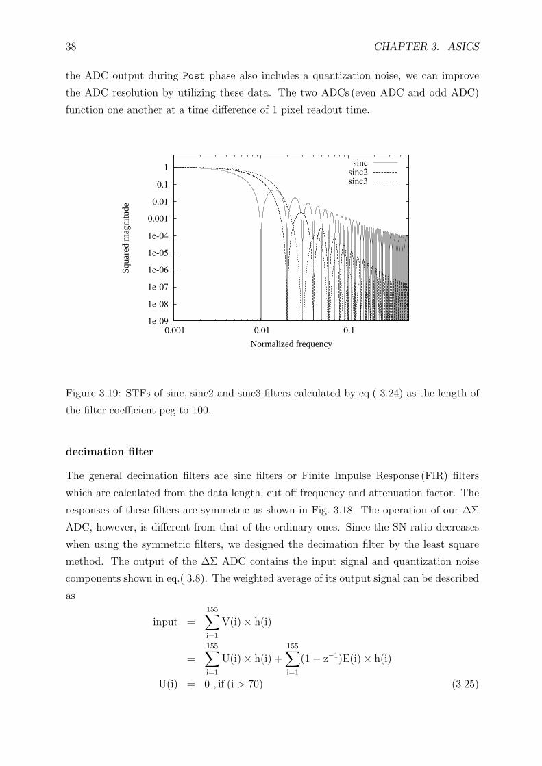
38 CHAPTER 3. ASICS
the ADC output during Post phase also includes a quantization noise, we can improve
the ADC resolution by utilizing these data. The two ADCs (even ADC and odd ADC)
function one another at a time difference of 1 pixel readout time.
1e-09
1e-08
1e-07
1e-06
1e-05
1e-04
0.001
0.01
0.1
1
0.001 0.01 0.1
Squa
red
mag
nitu
de
Normalized frequency
12bit ADC
sinc
sinc2
sinc3
Figure 3.19: STFs of sinc, sinc2 and sinc3 filters calculated by eq.( 3.24) as the length of
the filter coefficient peg to 100.
decimation filter
The general decimation filters are sinc filters or Finite Impulse Response (FIR) filters
which are calculated from the data length, cut-off frequency and attenuation factor. The
responses of these filters are symmetric as shown in Fig. 3.18. The operation of our ∆Σ
ADC, however, is different from that of the ordinary ones. Since the SN ratio decreases
when using the symmetric filters, we designed the decimation filter by the least square
method. The output of the ∆Σ ADC contains the input signal and quantization noise
components shown in eq.( 3.8). The weighted average of its output signal can be described
as
input =155∑i=1
V(i) × h(i)
=155∑i=1
U(i) × h(i) +155∑i=1
(1 − z−1)E(i) × h(i)
U(i) = 0 , if (i > 70) (3.25)
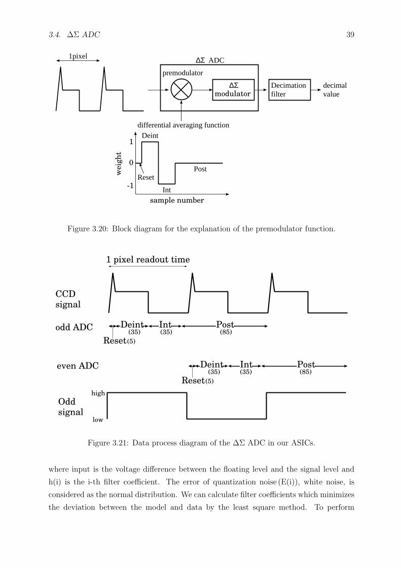
3.4. ∆Σ ADC 39
weig
ht
sample number
1
0
-1
∆Σmodulator
1pixel
Decimationfilter
premodulator
decimalvalue
differential averaging function
∆Σ ADC
Reset
Deint
Int
Post
Figure 3.20: Block diagram for the explanation of the premodulator function.
Deint Int Post
CCDsignal
odd ADC
Deint Int Post
Reset
Reset
even ADC
1 pixel readout time
(5)
(35) (35) (85)
(35) (35) (85)
(5)
Oddsignal
high
low
Figure 3.21: Data process diagram of the ∆Σ ADC in our ASICs.
where input is the voltage difference between the floating level and the signal level and
h(i) is the i-th filter coefficient. The error of quantization noise (E(i)), white noise, is
considered as the normal distribution. We can calculate filter coefficients which minimizes
the deviation between the model and data by the least square method. To perform
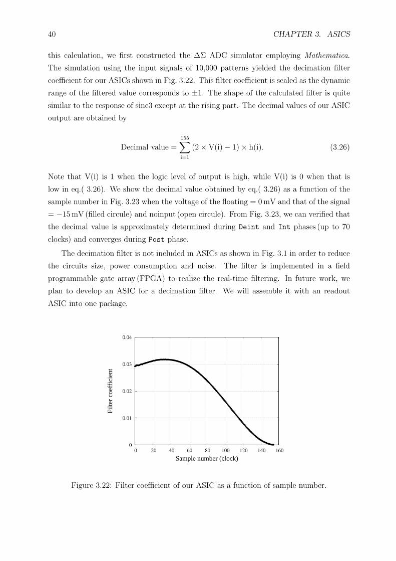
40 CHAPTER 3. ASICS
this calculation, we first constructed the ∆Σ ADC simulator employing Mathematica.
The simulation using the input signals of 10,000 patterns yielded the decimation filter
coefficient for our ASICs shown in Fig. 3.22. This filter coefficient is scaled as the dynamic
range of the filtered value corresponds to ±1. The shape of the calculated filter is quite
similar to the response of sinc3 except at the rising part. The decimal values of our ASIC
output are obtained by
Decimal value =155∑i=1
(2 × V(i) − 1) × h(i). (3.26)
Note that V(i) is 1 when the logic level of output is high, while V(i) is 0 when that is
low in eq.( 3.26). We show the decimal value obtained by eq.( 3.26) as a function of the
sample number in Fig. 3.23 when the voltage of the floating = 0 mV and that of the signal
= −15mV (filled circule) and noinput (open circule). From Fig. 3.23, we can verified that
the decimal value is approximately determined during Deint and Int phases (up to 70
clocks) and converges during Post phase.
The decimation filter is not included in ASICs as shown in Fig. 3.1 in order to reduce
the circuits size, power consumption and noise. The filter is implemented in a field
programmable gate array (FPGA) to realize the real-time filtering. In future work, we
plan to develop an ASIC for a decimation filter. We will assemble it with an readout
ASIC into one package.
0
0.01
0.02
0.03
0.04
0 20 40 60 80 100 120 140 160
Filte
r co
effi
cien
t
Sample number (clock)
Figure 3.22: Filter coefficient of our ASIC as a function of sample number.
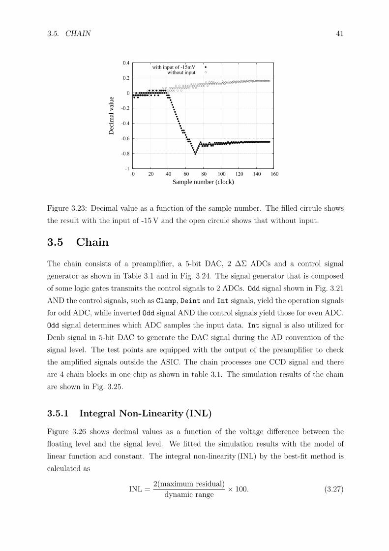
3.5. CHAIN 41
-1
-0.8
-0.6
-0.4
-0.2
0
0.2
0.4
0 20 40 60 80 100 120 140 160
Dec
imal
val
ue
Sample number (clock)
with input of -15mVwithout input
Figure 3.23: Decimal value as a function of the sample number. The filled circule shows
the result with the input of -15V and the open circule shows that without input.
3.5 Chain
The chain consists of a preamplifier, a 5-bit DAC, 2 ∆Σ ADCs and a control signal
generator as shown in Table 3.1 and in Fig. 3.24. The signal generator that is composed
of some logic gates transmits the control signals to 2 ADCs. Odd signal shown in Fig. 3.21
AND the control signals, such as Clamp, Deint and Int signals, yield the operation signals
for odd ADC, while inverted Odd signal AND the control signals yield those for even ADC.
Odd signal determines which ADC samples the input data. Int signal is also utilized for
Denb signal in 5-bit DAC to generate the DAC signal during the AD convention of the
signal level. The test points are equipped with the output of the preamplifier to check
the amplified signals outside the ASIC. The chain processes one CCD signal and there
are 4 chain blocks in one chip as shown in table 3.1. The simulation results of the chain
are shown in Fig. 3.25.
3.5.1 Integral Non-Linearity (INL)
Figure 3.26 shows decimal values as a function of the voltage difference between the
floating level and the signal level. We fitted the simulation results with the model of
linear function and constant. The integral non-linearity (INL) by the best-fit method is
calculated as
INL =2(maximum residual)
dynamic range× 100. (3.27)
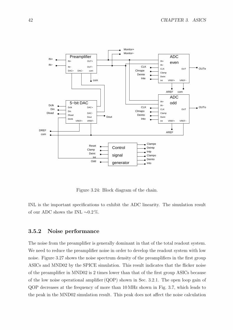
42 CHAPTER 3. ASICS
IN+
IN−
DREFcom
com
DclkDin
DloadDout
AREF
OUTeClmape
DeinteInte
CLK
ClmapoDeinto
Into
CLK OUTo
AREF com
Monitor+Monitor−
DAC+ DAC−
Preamplifier
com
IN+
IN−
OUT+
OUT−
VREF+ VREF−
5−bit DAC
Din
Dload
DAC+
DAC−
Denb
Dclk
Dout
even
odd
Control
signal
generator
ClampeDeintpIntpClampoDeintoInto
ResetClamp
Deint
OddInt
VREF+ VREF−
ADCIN+
IN−
OUTCLK
Deint
Int
Clamp
VREF+ VREF−
ADCIN+
IN−
OUTCLK
Deint
Int
Clamp
Figure 3.24: Block diagram of the chain.
INL is the important specifications to exhibit the ADC linearity. The simulation result
of our ADC shows the INL ∼0.2%.
3.5.2 Noise performance
The noise from the preamplifier is generally dominant in that of the total readout system.
We need to reduce the preamplifier noise in order to develop the readout system with low
noise. Figure 3.27 shows the noise spectrum density of the preamplifiers in the first group
ASICs and MND02 by the SPICE simulation. This result indicates that the flicker noise
of the preamplifier in MND02 is 2 times lower than that of the first group ASICs because
of the low noise operational amplifier (QOP) shown in Sec. 3.2.1. The open loop gain of
QOP decreases at the frequency of more than 10MHz shown in Fig. 3.7, which leads to
the peak in the MND02 simulation result. This peak does not affect the noise calculation

3.5. CHAIN 43
0
2
4
0 1 2 3 4 5
outp
ut E
VE
N A
DC
Time (us)
(e)
0
2
4
Inte
(d) 0
2
4
Dei
nte (c)
0
2
4
Cla
mpe (b)
-0.01
0.01
0.03
0.05
inpu
t (V
) (a)
0
2
4
0 1 2 3 4 5
outp
ut O
DD
AD
C
Time (us)
(e)
0
2
4
Into
(d) 0
2
4
Dei
nto (c)
0
2
4
Cla
mpo (b)
-0.01
0.01
0.03
0.05
inpu
t (V
) (a)
Figure 3.25: Simulation results of the chain. (a)∼(e) are an input signal of the chain,
Clamp, Deint, Int signals and bitstream (left : even ADC) and (right : odd ADC), respec-
tively.
-0.1
0
0.1
-0.02 -0.015 -0.01 -0.005 0 0.005 0.01 0.015 0.02
Res
idua
l (%
)
Voltage difference (V)
(b)-1
-0.8
-0.6
-0.4
-0.2
0
0.2
0.4
0.6
0.8
1
Dec
imal
val
ue
(a)
data
model
Figure 3.26: Linearity of the chain. The filled circle is simulation results and the solid
line is the best fit model of the linear function in (a), and (b) shows the residual between
the data and model.
because the noise at the frequency of less than 1MHz is the dominant in the result.
The STF of the ∆Σ ADC can be considered as the multi-sampling method explained
in Sec. 2.3.2
|H(f)total|2 = |H(f)sample|2 × |H(f)cds|2 =
(2
35
sin(35πfTclk)
sin(πfTclk)sin(πfTcds)
)2
(3.28)
where 35 is the number of sample during Deint and Int phases, Tcds is the sample-to-
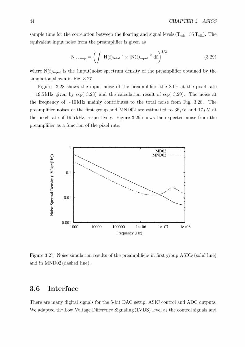
44 CHAPTER 3. ASICS
sample time for the correlation between the floating and signal levels (Tcds=35Tclk). The
equivalent input noise from the preamplifier is given as
Npreamp =
(∫|H(f)total|2 × |N(f)input|2 df
)1/2
(3.29)
where N(f)input is the (input)noise spectrum density of the preamplifier obtained by the
simulation shown in Fig. 3.27.
Figure 3.28 shows the input noise of the preamplifier, the STF at the pixel rate
= 19.5 kHz given by eq.( 3.28) and the calculation result of eq.( 3.29). The noise at
the frequency of ∼10 kHz mainly contributes to the total noise from Fig. 3.28. The
preamplifier noises of the first group and MND02 are estimated to 36µV and 17µV at
the pixel rate of 19.5 kHz, respectively. Figure 3.29 shows the expected noise from the
preamplifier as a function of the pixel rate.
0.001
0.01
0.1
1
1000 10000 100000 1e+06 1e+07 1e+08
Noi
se S
pect
ral D
ensi
ty (
uV/s
qrt(
Hz)
)
Frequency (Hz)
MD02
MND02
Figure 3.27: Noise simulation results of the preamplifiers in first group ASICs (solid line)
and in MND02 (dashed line).
3.6 Interface
There are many digital signals for the 5-bit DAC setup, ASIC control and ADC outputs.
We adapted the Low Voltage Difference Signaling (LVDS) level as the control signals and
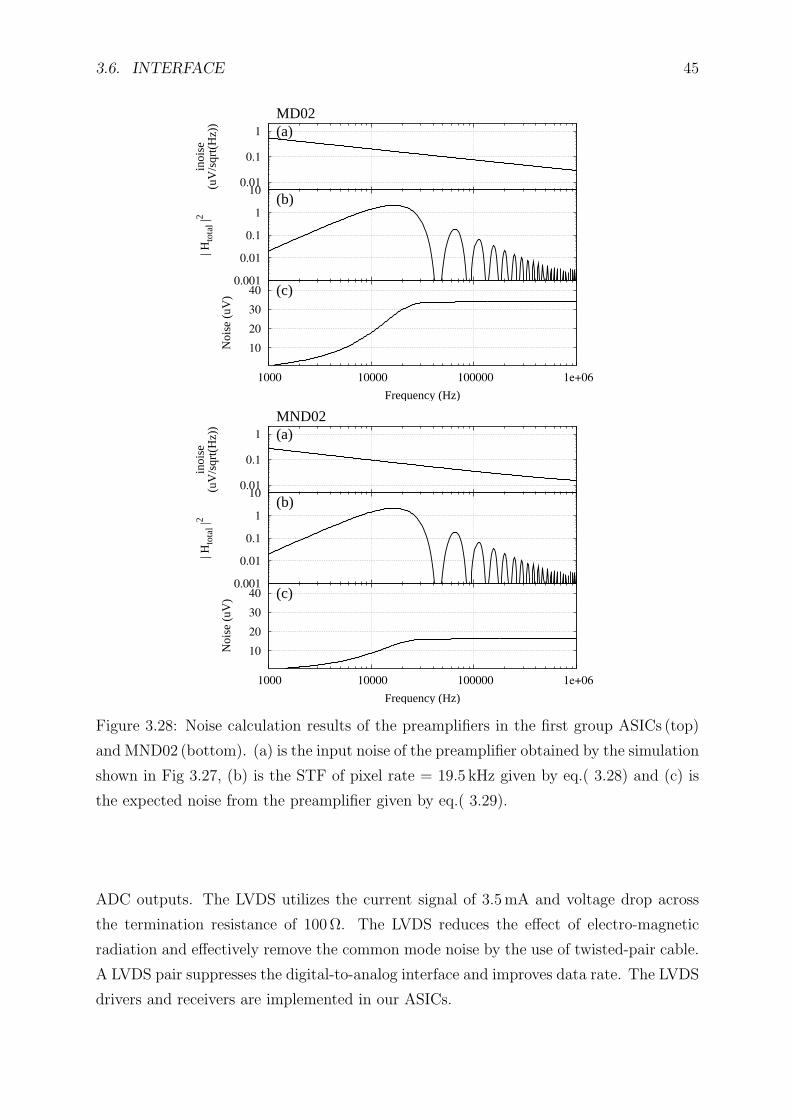
3.6. INTERFACE 45
10
20
30
40
1000 10000 100000 1e+06
Noi
se (
uV)
Frequency (Hz)
(c) 0.001
0.01
0.1
1
10
| Hto
tal |
2(b)
0.01
0.1
1
inoi
se(u
V/s
qrt(
Hz)
)
MD02(a)
10
20
30
40
1000 10000 100000 1e+06
Noi
se (
uV)
Frequency (Hz)
(c) 0.001
0.01
0.1
1
10
| Hto
tal |
2
(b) 0.01
0.1
1
inoi
se(u
V/s
qrt(
Hz)
)
MND02(a)
Figure 3.28: Noise calculation results of the preamplifiers in the first group ASICs (top)
and MND02 (bottom). (a) is the input noise of the preamplifier obtained by the simulation
shown in Fig 3.27, (b) is the STF of pixel rate = 19.5 kHz given by eq.( 3.28) and (c) is
the expected noise from the preamplifier given by eq.( 3.29).
ADC outputs. The LVDS utilizes the current signal of 3.5 mA and voltage drop across
the termination resistance of 100Ω. The LVDS reduces the effect of electro-magnetic
radiation and effectively remove the common mode noise by the use of twisted-pair cable.
A LVDS pair suppresses the digital-to-analog interface and improves data rate. The LVDS
drivers and receivers are implemented in our ASICs.
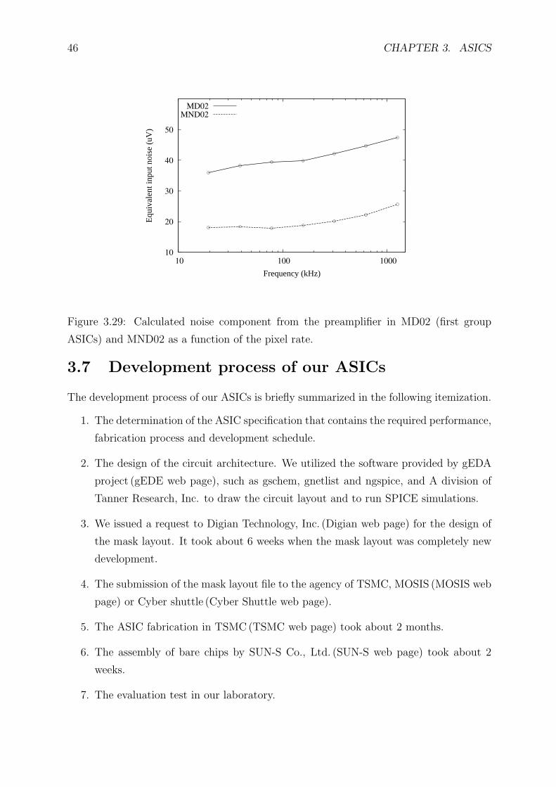
46 CHAPTER 3. ASICS
10
20
30
40
50
10 100 1000
Equ
ival
ent i
nput
noi
se (
uV)
Frequency (kHz)
MD02
MND02
Figure 3.29: Calculated noise component from the preamplifier in MD02 (first group
ASICs) and MND02 as a function of the pixel rate.
3.7 Development process of our ASICs
The development process of our ASICs is briefly summarized in the following itemization.
1. The determination of the ASIC specification that contains the required performance,
fabrication process and development schedule.
2. The design of the circuit architecture. We utilized the software provided by gEDA
project (gEDE web page), such as gschem, gnetlist and ngspice, and A division of
Tanner Research, Inc. to draw the circuit layout and to run SPICE simulations.
3. We issued a request to Digian Technology, Inc. (Digian web page) for the design of
the mask layout. It took about 6 weeks when the mask layout was completely new
development.
4. The submission of the mask layout file to the agency of TSMC, MOSIS (MOSIS web
page) or Cyber shuttle (Cyber Shuttle web page).
5. The ASIC fabrication in TSMC (TSMC web page) took about 2 months.
6. The assembly of bare chips by SUN-S Co., Ltd. (SUN-S web page) took about 2
weeks.
7. The evaluation test in our laboratory.
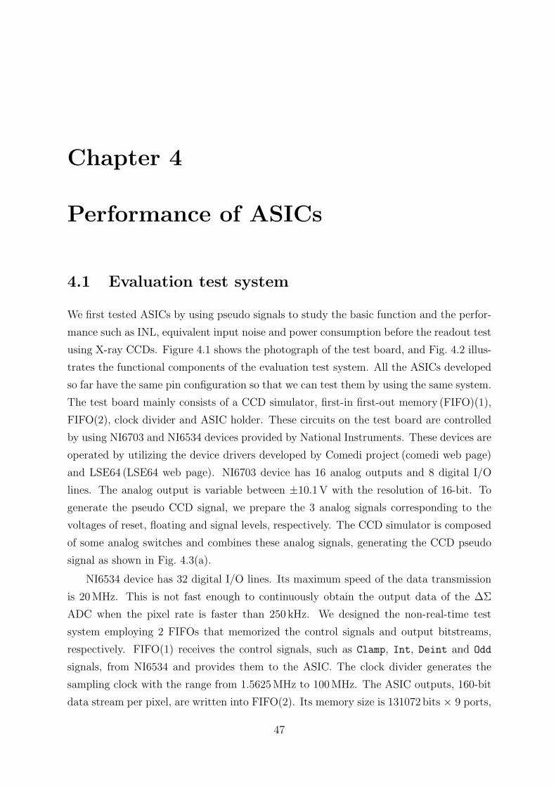
Chapter 4
Performance of ASICs
4.1 Evaluation test system
We first tested ASICs by using pseudo signals to study the basic function and the perfor-
mance such as INL, equivalent input noise and power consumption before the readout test
using X-ray CCDs. Figure 4.1 shows the photograph of the test board, and Fig. 4.2 illus-
trates the functional components of the evaluation test system. All the ASICs developed
so far have the same pin configuration so that we can test them by using the same system.
The test board mainly consists of a CCD simulator, first-in first-out memory (FIFO)(1),
FIFO(2), clock divider and ASIC holder. These circuits on the test board are controlled
by using NI6703 and NI6534 devices provided by National Instruments. These devices are
operated by utilizing the device drivers developed by Comedi project (comedi web page)
and LSE64 (LSE64 web page). NI6703 device has 16 analog outputs and 8 digital I/O
lines. The analog output is variable between ±10.1V with the resolution of 16-bit. To
generate the pseudo CCD signal, we prepare the 3 analog signals corresponding to the
voltages of reset, floating and signal levels, respectively. The CCD simulator is composed
of some analog switches and combines these analog signals, generating the CCD pseudo
signal as shown in Fig. 4.3(a).
NI6534 device has 32 digital I/O lines. Its maximum speed of the data transmission
is 20 MHz. This is not fast enough to continuously obtain the output data of the ∆Σ
ADC when the pixel rate is faster than 250 kHz. We designed the non-real-time test
system employing 2 FIFOs that memorized the control signals and output bitstreams,
respectively. FIFO(1) receives the control signals, such as Clamp, Int, Deint and Odd
signals, from NI6534 and provides them to the ASIC. The clock divider generates the
sampling clock with the range from 1.5625 MHz to 100MHz. The ASIC outputs, 160-bit
data stream per pixel, are written into FIFO(2). Its memory size is 131072 bits × 9 ports,
47
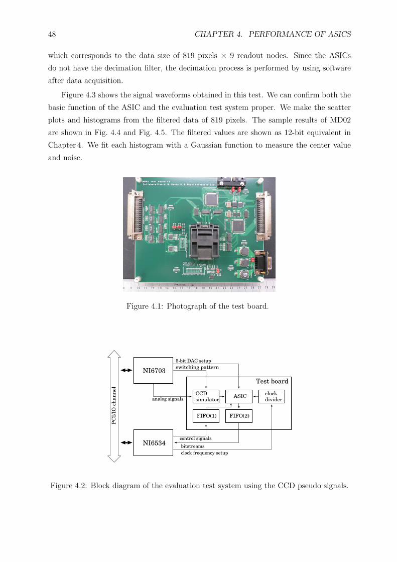
48 CHAPTER 4. PERFORMANCE OF ASICS
which corresponds to the data size of 819 pixels × 9 readout nodes. Since the ASICs
do not have the decimation filter, the decimation process is performed by using software
after data acquisition.
Figure 4.3 shows the signal waveforms obtained in this test. We can confirm both the
basic function of the ASIC and the evaluation test system proper. We make the scatter
plots and histograms from the filtered data of 819 pixels. The sample results of MD02
are shown in Fig. 4.4 and Fig. 4.5. The filtered values are shown as 12-bit equivalent in
Chapter 4. We fit each histogram with a Gaussian function to measure the center value
and noise.
Figure 4.1: Photograph of the test board.
Test board
NI6703
NI6534
PC
I/IO
ch
an
nel
CCDsimulator
FIFO(1) FIFO(2)
ASICclockdivider
switching pattern
5-bit DAC setup
control signals
bitstreams
clock frequency setup
analog signals
Figure 4.2: Block diagram of the evaluation test system using the CCD pseudo signals.
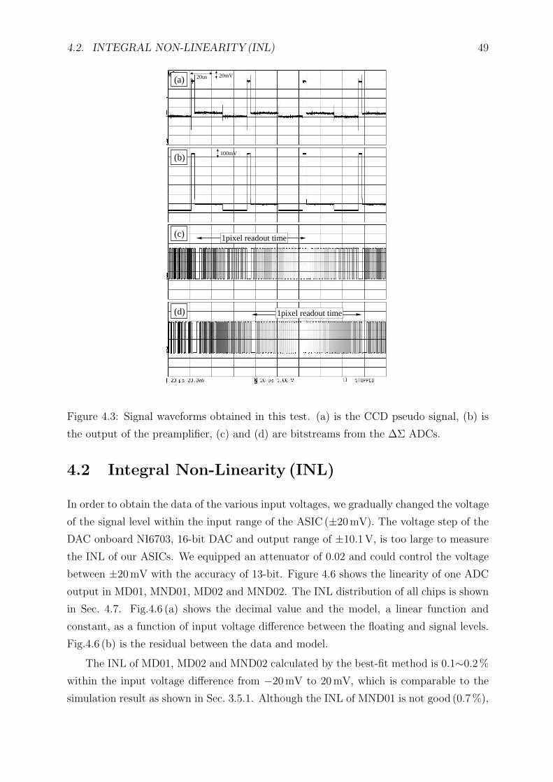
4.2. INTEGRAL NON-LINEARITY (INL) 49
20us 20mV
100mV
(a)
(d)
(c)
(b)
1pixel readout time
1pixel readout time
Figure 4.3: Signal waveforms obtained in this test. (a) is the CCD pseudo signal, (b) is
the output of the preamplifier, (c) and (d) are bitstreams from the ∆Σ ADCs.
4.2 Integral Non-Linearity (INL)
In order to obtain the data of the various input voltages, we gradually changed the voltage
of the signal level within the input range of the ASIC (±20mV). The voltage step of the
DAC onboard NI6703, 16-bit DAC and output range of ±10.1V, is too large to measure
the INL of our ASICs. We equipped an attenuator of 0.02 and could control the voltage
between ±20mV with the accuracy of 13-bit. Figure 4.6 shows the linearity of one ADC
output in MD01, MND01, MD02 and MND02. The INL distribution of all chips is shown
in Sec. 4.7. Fig.4.6 (a) shows the decimal value and the model, a linear function and
constant, as a function of input voltage difference between the floating and signal levels.
Fig.4.6 (b) is the residual between the data and model.
The INL of MD01, MD02 and MND02 calculated by the best-fit method is 0.1∼0.2%
within the input voltage difference from −20mV to 20 mV, which is comparable to the
simulation result as shown in Sec. 3.5.1. Although the INL of MND01 is not good (0.7%),
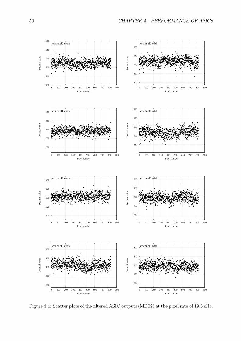
50 CHAPTER 4. PERFORMANCE OF ASICS
1710
1720
1730
1740
1750
1760
0 100 200 300 400 500 600 700 800 900
Dec
imal
val
ue
Pixel number
channel0 even
1820
1830
1840
1850
1860
0 100 200 300 400 500 600 700 800 900
Dec
imal
val
ue
Pixel number
channel0 odd
1620
1630
1640
1650
1660
0 100 200 300 400 500 600 700 800 900
Dec
imal
val
ue
Pixel number
channel1 even
1880
1890
1900
1910
1920
0 100 200 300 400 500 600 700 800 900
Dec
imal
val
ue
Pixel number
channel1 odd
1710
1720
1730
1740
1750
0 100 200 300 400 500 600 700 800 900
Dec
imal
val
ue
Pixel number
channel2 even
1760
1770
1780
1790
1800
0 100 200 300 400 500 600 700 800 900
Dec
imal
val
ue
Pixel number
channel2 odd
1390
1400
1410
1420
1430
0 100 200 300 400 500 600 700 800 900
Dec
imal
val
ue
Pixel number
channel3 even
1810
1820
1830
1840
1850
0 100 200 300 400 500 600 700 800 900
Dec
imal
val
ue
Pixel number
channel3 odd
Figure 4.4: Scatter plots of the filtered ASIC outputs (MD02) at the pixel rate of 19.5 kHz.
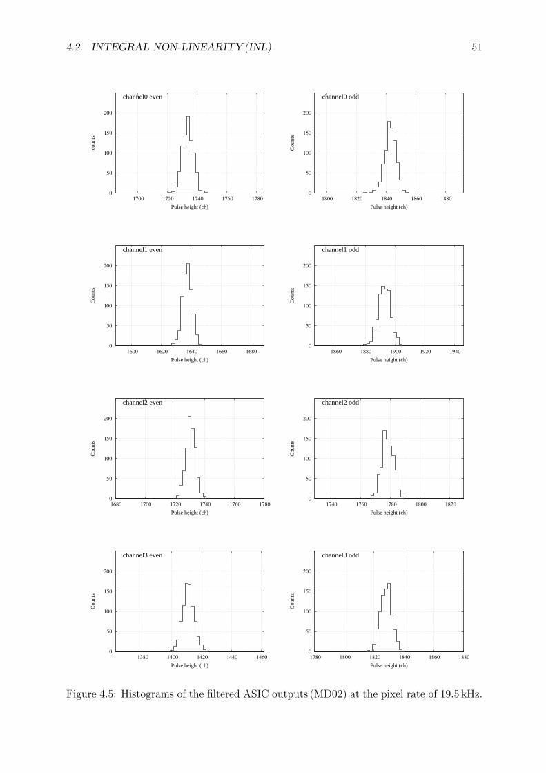
4.2. INTEGRAL NON-LINEARITY (INL) 51
0
50
100
150
200
1700 1720 1740 1760 1780
coun
ts
Pulse height (ch)
channel0 even
0
50
100
150
200
1800 1820 1840 1860 1880
Cou
nts
Pulse height (ch)
channel0 odd
0
50
100
150
200
1600 1620 1640 1660 1680
Cou
nts
Pulse height (ch)
channel1 even
0
50
100
150
200
1860 1880 1900 1920 1940
Cou
nts
Pulse height (ch)
channel1 odd
0
50
100
150
200
1680 1700 1720 1740 1760 1780
Cou
nts
Pulse height (ch)
channel2 even
0
50
100
150
200
1740 1760 1780 1800 1820
Cou
nts
Pulse height (ch)
channel2 odd
0
50
100
150
200
1380 1400 1420 1440 1460
Cou
nts
Pulse height (ch)
channel3 even
0
50
100
150
200
1780 1800 1820 1840 1860 1880
Cou
nts
Pulse height (ch)
channel3 odd
Figure 4.5: Histograms of the filtered ASIC outputs (MD02) at the pixel rate of 19.5 kHz.
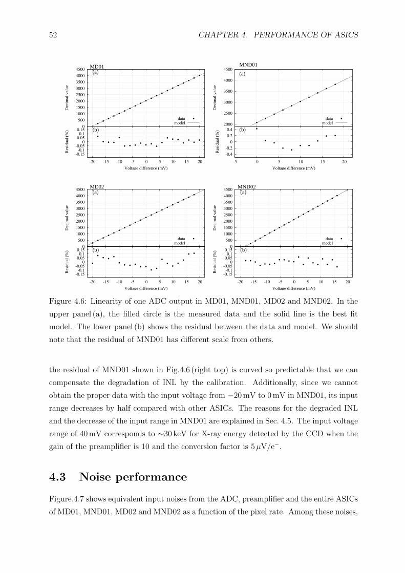
52 CHAPTER 4. PERFORMANCE OF ASICS
-0.15
-0.1
-0.05
0
0.05
0.1
0.15
-20 -15 -10 -5 0 5 10 15 20
Res
idua
l (%
)
Voltage difference (mV)
(b) 0
500
1000
1500
2000
2500
3000
3500
4000
4500D
ecim
al v
alue
MD01(a)
data
model
-0.4
-0.2
0
0.2
0.4
-5 0 5 10 15 20
Res
idua
l (%
)
Voltage difference (mV)
(b) 2000
2500
3000
3500
4000
4500
Dec
imal
val
ue
MND01
(a)
data
model
-0.15
-0.1
-0.05
0
0.05
0.1
0.15
-20 -15 -10 -5 0 5 10 15 20
Res
idua
l (%
)
Voltage difference (mV)
(b) 0
500
1000
1500
2000
2500
3000
3500
4000
4500
Dec
imal
val
ue
MD02(a)
data
model
-0.15
-0.1
-0.05
0
0.05
0.1
0.15
-20 -15 -10 -5 0 5 10 15 20
Res
idua
l (%
)
Voltage difference (mV)
(b) 0
500
1000
1500
2000
2500
3000
3500
4000
4500
Dec
imal
val
ue
MND02(a)
data
model
Figure 4.6: Linearity of one ADC output in MD01, MND01, MD02 and MND02. In the
upper panel (a), the filled circle is the measured data and the solid line is the best fit
model. The lower panel (b) shows the residual between the data and model. We should
note that the residual of MND01 has different scale from others.
the residual of MND01 shown in Fig.4.6 (right top) is curved so predictable that we can
compensate the degradation of INL by the calibration. Additionally, since we cannot
obtain the proper data with the input voltage from −20mV to 0 mV in MND01, its input
range decreases by half compared with other ASICs. The reasons for the degraded INL
and the decrease of the input range in MND01 are explained in Sec. 4.5. The input voltage
range of 40mV corresponds to ∼30 keV for X-ray energy detected by the CCD when the
gain of the preamplifier is 10 and the conversion factor is 5µV/e−.
4.3 Noise performance
Figure.4.7 shows equivalent input noises from the ADC, preamplifier and the entire ASICs
of MD01, MND01, MD02 and MND02 as a function of the pixel rate. Among these noises,
4.4. POWER CONSUMPTION 53
the noise from the preamplifier cannot be directly measured. We first obtain the noises
from the ADC and the entire ASIC, and calculate the residual between these values as
the preamplifier noise. The noise simulation results estimated in Sec. 3.5.2 are also shown
in the figures of MD02 and MND02. The equivalent input noise of MD02 is 41.0±0.3µV,
ADC = 20.5±0.2µV and preamplifier = 35.5±0.5µV at the pixel rate of 156 kHz. The
preamplifier noise is dominant in the total noise of MD02 from the test results. The
calculation value in Fig.4.7 agrees with the measured data. We succeeded in establishing
the calculation method of the preamplifier noise.
We considered the flicker noise from the preamplifier as the main noise source in MD02
as shown in Fig. 3.28. We implemented the low noise operational amplifier in MND02 to
suppress the flicker noise of the preamplifier. The calculated noise from the preamplifier
in MND02 is 19µV at the pixel rate of 156 kHz, which is about half that in MD02.
The measured noise of MND02 is 29.4±0.3µV, ADC = 18.7±0.2µV and preamplifier =
22.3±0.5µV at the pixel rate of 156 kHz. We decreased the preamplifier noise by 40% as
the calculation results. The noise distribution of all chips is shown in Sec. 4.7. The ADC
noise has a tendency to rapidly increase at the pixel rate of more than 312 kHz. We are
currently studying the source of this result. We will evaluate the frequency characteristic
of the bitstreams by Discrete Fourier Transform (DFT), and change the decimation filter
coefficient.
An Equivalent Noise Charge (ENC) depends on a conversion factor in the readout test
using CCDs. The ENC can be described as
ENC =Equivalent input noise (µV)
Conversion factor (µV/e−). (4.1)
Assuming the conversion factor of 5µV/e−, the ENCs of MD02 and MND02 are expected
to be about 7 and 5 electrons, respectively. The ratio of the ASIC noise to the total
system noise decreases with increasing the conversion factor.
4.4 Power consumption
Figure 4.8 shows the power consumption per chip as a function of the pixel rate. The
power consumption of MND01 and MD02 is about 90 mW/chip at the 156 kHz pixel rate.
Note that the power of MD01 at the high pixel rate of more than ∼200 kHz dose not change
due to the malfunction of the digital circuits as explained in § 4.5. The difference of the
power consumption between MND02 and other chips is caused by the current of LVDS
drive. The signal current and termination resistance in the normal LVDS level are 3.5mA
and 100Ω, respectively. In MD01, MND01 and MD02, we changed the signal current
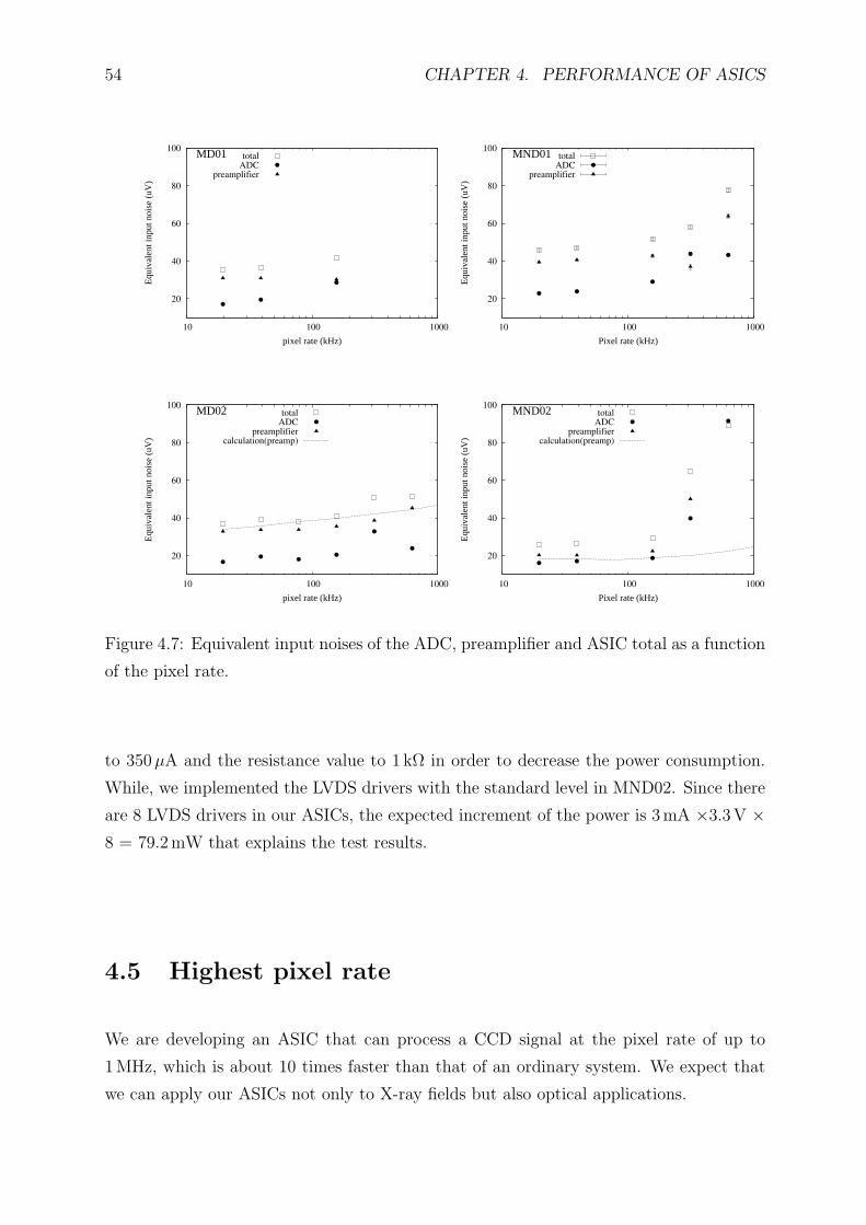
54 CHAPTER 4. PERFORMANCE OF ASICS
20
40
60
80
100
10 100 1000
Equ
ival
ent i
nput
noi
se (
uV)
pixel rate (kHz)
MD01 totalADC
preamplifier
20
40
60
80
100
10 100 1000
Equ
ival
ent i
nput
noi
se (
uV)
Pixel rate (kHz)
MND01 totalADC
preamplifier
20
40
60
80
100
10 100 1000
Equ
ival
ent i
nput
noi
se (
uV)
pixel rate (kHz)
MD02 totalADC
preamplifiercalculation(preamp)
20
40
60
80
100
10 100 1000
Equ
ival
ent i
nput
noi
se (
uV)
Pixel rate (kHz)
MND02 totalADC
preamplifiercalculation(preamp)
Figure 4.7: Equivalent input noises of the ADC, preamplifier and ASIC total as a function
of the pixel rate.
to 350µA and the resistance value to 1 kΩ in order to decrease the power consumption.
While, we implemented the LVDS drivers with the standard level in MND02. Since there
are 8 LVDS drivers in our ASICs, the expected increment of the power is 3 mA ×3.3V ×8 = 79.2 mW that explains the test results.
4.5 Highest pixel rate
We are developing an ASIC that can process a CCD signal at the pixel rate of up to
1 MHz, which is about 10 times faster than that of an ordinary system. We expect that
we can apply our ASICs not only to X-ray fields but also optical applications.
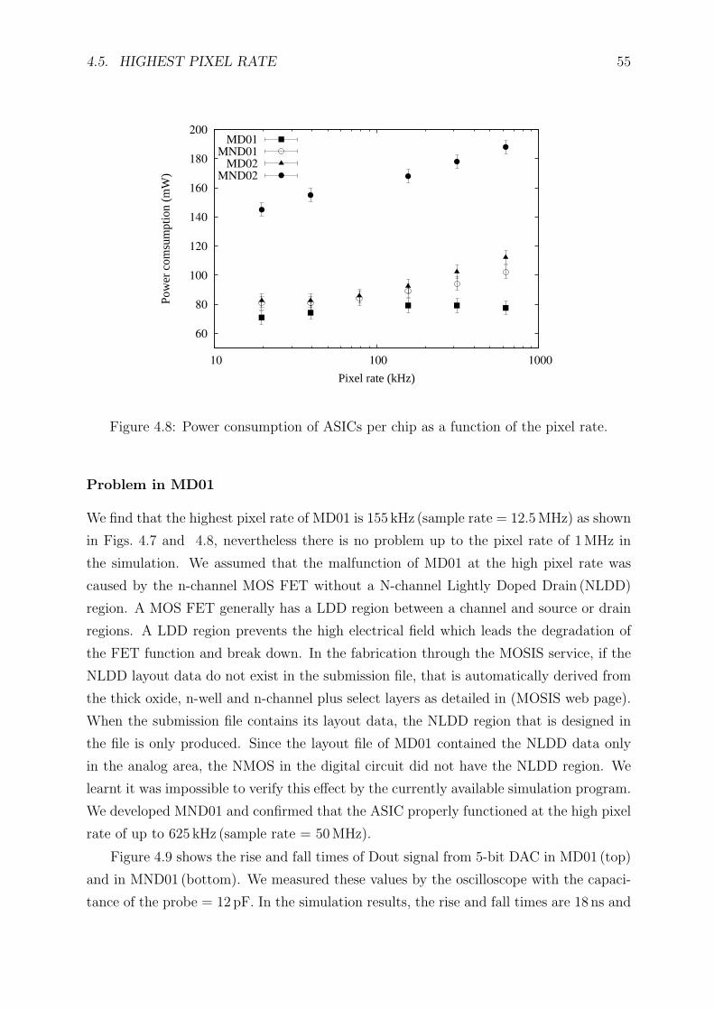
4.5. HIGHEST PIXEL RATE 55
60
80
100
120
140
160
180
200
10 100 1000
Pow
er c
omsu
mpt
ion
(mW
)
Pixel rate (kHz)
MD01
MND01
MD02
MND02
Figure 4.8: Power consumption of ASICs per chip as a function of the pixel rate.
Problem in MD01
We find that the highest pixel rate of MD01 is 155 kHz (sample rate = 12.5MHz) as shown
in Figs. 4.7 and 4.8, nevertheless there is no problem up to the pixel rate of 1MHz in
the simulation. We assumed that the malfunction of MD01 at the high pixel rate was
caused by the n-channel MOS FET without a N-channel Lightly Doped Drain (NLDD)
region. A MOS FET generally has a LDD region between a channel and source or drain
regions. A LDD region prevents the high electrical field which leads the degradation of
the FET function and break down. In the fabrication through the MOSIS service, if the
NLDD layout data do not exist in the submission file, that is automatically derived from
the thick oxide, n-well and n-channel plus select layers as detailed in (MOSIS web page).
When the submission file contains its layout data, the NLDD region that is designed in
the file is only produced. Since the layout file of MD01 contained the NLDD data only
in the analog area, the NMOS in the digital circuit did not have the NLDD region. We
learnt it was impossible to verify this effect by the currently available simulation program.
We developed MND01 and confirmed that the ASIC properly functioned at the high pixel
rate of up to 625 kHz (sample rate = 50MHz).
Figure 4.9 shows the rise and fall times of Dout signal from 5-bit DAC in MD01 (top)
and in MND01 (bottom). We measured these values by the oscilloscope with the capaci-
tance of the probe = 12 pF. In the simulation results, the rise and fall times are 18 ns and
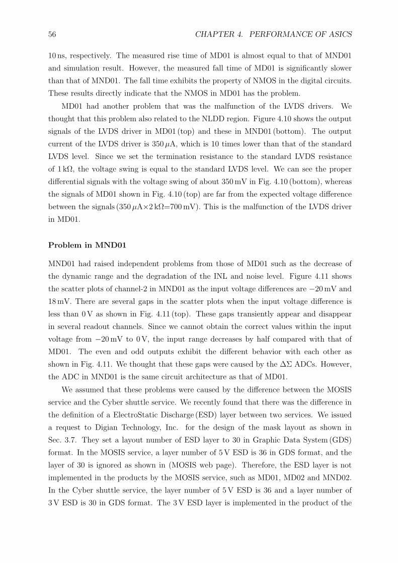
56 CHAPTER 4. PERFORMANCE OF ASICS
10 ns, respectively. The measured rise time of MD01 is almost equal to that of MND01
and simulation result. However, the measured fall time of MD01 is significantly slower
than that of MND01. The fall time exhibits the property of NMOS in the digital circuits.
These results directly indicate that the NMOS in MD01 has the problem.
MD01 had another problem that was the malfunction of the LVDS drivers. We
thought that this problem also related to the NLDD region. Figure 4.10 shows the output
signals of the LVDS driver in MD01 (top) and these in MND01 (bottom). The output
current of the LVDS driver is 350µA, which is 10 times lower than that of the standard
LVDS level. Since we set the termination resistance to the standard LVDS resistance
of 1 kΩ, the voltage swing is equal to the standard LVDS level. We can see the proper
differential signals with the voltage swing of about 350mV in Fig. 4.10 (bottom), whereas
the signals of MD01 shown in Fig. 4.10 (top) are far from the expected voltage difference
between the signals (350µA×2 kΩ=700mV). This is the malfunction of the LVDS driver
in MD01.
Problem in MND01
MND01 had raised independent problems from those of MD01 such as the decrease of
the dynamic range and the degradation of the INL and noise level. Figure 4.11 shows
the scatter plots of channel-2 in MND01 as the input voltage differences are −20mV and
18 mV. There are several gaps in the scatter plots when the input voltage difference is
less than 0V as shown in Fig. 4.11 (top). These gaps transiently appear and disappear
in several readout channels. Since we cannot obtain the correct values within the input
voltage from −20mV to 0V, the input range decreases by half compared with that of
MD01. The even and odd outputs exhibit the different behavior with each other as
shown in Fig. 4.11. We thought that these gaps were caused by the ∆Σ ADCs. However,
the ADC in MND01 is the same circuit architecture as that of MD01.
We assumed that these problems were caused by the difference between the MOSIS
service and the Cyber shuttle service. We recently found that there was the difference in
the definition of a ElectroStatic Discharge (ESD) layer between two services. We issued
a request to Digian Technology, Inc. for the design of the mask layout as shown in
Sec. 3.7. They set a layout number of ESD layer to 30 in Graphic Data System (GDS)
format. In the MOSIS service, a layer number of 5V ESD is 36 in GDS format, and the
layer of 30 is ignored as shown in (MOSIS web page). Therefore, the ESD layer is not
implemented in the products by the MOSIS service, such as MD01, MD02 and MND02.
In the Cyber shuttle service, the layer number of 5V ESD is 36 and a layer number of
3 V ESD is 30 in GDS format. The 3V ESD layer is implemented in the product of the
4.5. HIGHEST PIXEL RATE 57
(a)
(b)
MD011V
10us
(a)
(b)
MND011V
10us
Figure 4.9: Rise and fall times of Dout signals in MD01 (top) and in MND01 (bottom).
(a) is the signal waveforms and (b) shows the results measured by the oscilloscope with
the capacitance of the probe = 12 pF.
Cyber shuttle service, MND01. To investigate the effect from this difference, we fabricated
MD02 whose circuits were the identical to that of MD01 except for the NLDD layer by
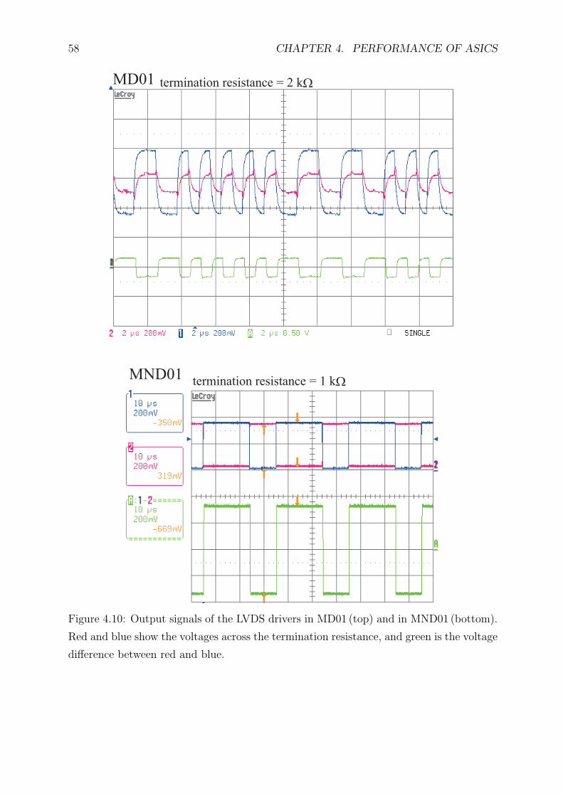
58 CHAPTER 4. PERFORMANCE OF ASICS
MD01 termination resistance = 2 kΩ
MND01termination resistance = 1 kΩ
Figure 4.10: Output signals of the LVDS drivers in MD01 (top) and in MND01 (bottom).
Red and blue show the voltages across the termination resistance, and green is the voltage
difference between red and blue.
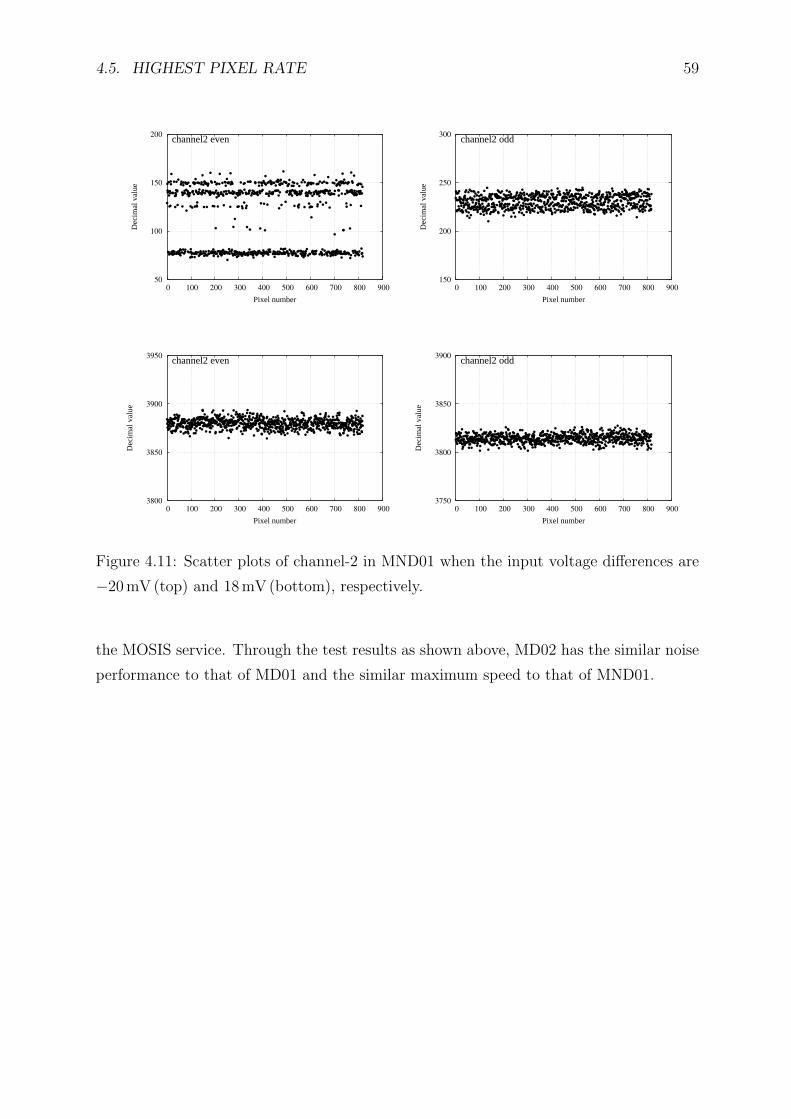
4.5. HIGHEST PIXEL RATE 59
50
100
150
200
0 100 200 300 400 500 600 700 800 900
Dec
imal
val
ue
Pixel number
channel2 even
150
200
250
300
0 100 200 300 400 500 600 700 800 900
Dec
imal
val
ue
Pixel number
channel2 odd
3800
3850
3900
3950
0 100 200 300 400 500 600 700 800 900
Dec
imal
val
ue
Pixel number
channel2 even
3750
3800
3850
3900
0 100 200 300 400 500 600 700 800 900
Dec
imal
val
ue
Pixel number
channel2 odd
Figure 4.11: Scatter plots of channel-2 in MND01 when the input voltage differences are
−20 mV (top) and 18mV (bottom), respectively.
the MOSIS service. Through the test results as shown above, MD02 has the similar noise
performance to that of MD01 and the similar maximum speed to that of MND01.
60 CHAPTER 4. PERFORMANCE OF ASICS
4.6 Radiation test
4.6.1 Motivation
The motivation of the radiation test is to study total ionization dose (TID) effects of
our ASICs and verify that they can be employed as the front-end electronics onboard
the satellites. We are now designing the X-ray CCD camera system using our ASICs
for the SXI onboard ASTRO-H. The orbit of ASTRO-H will be the low earth orbit of
550 km similar to those of ASCA (Tanaka et al. 1994) and Suzaku (Mitsuda et al. 2007).
The radiation damage mainly occurs by the high-energy protons during passing through
the South Atlantic Anomaly (SAA). The estimated TID per year for the CCDs onboard
ASCA satellite is ∼0.2 krad (Yamashita et al. 1999). The CCDs are surrounded by the
shields with the average thickness of 11 g cm−2 aluminum (Al) equivalent to protect them
from protons and suppress the background level recorded by the CCDs. Since the readout
system is placed outside of the thick shield, the total absorption dose of the readout system
is generally estimated to ∼1 krad per year in this orbit. The typical lifetime of the satellite
is 5 years. The required radiation tolerance for our ASICs is more than 5 krad.
4.6.2 Test condition
We tested the radiation tolerance of MD01 using the accelerator proton beam from the
medium-energy accelerator in the Heavy Ion Medical Accelerator in Chiba (HIMAC) at
the National Institute of Radiological Science in Japan. The proton energy is 200MeV
and the beam size is 1 cm×1 cm. We adjusted the position of the beam center by using
a laser pointer and a phosphorplate. We measured the intensity of the proton beam by
using a scintillation counter. The average of the beam count rate is variable from 102∼108
protons per second with accuracy of 20% (Nakajima, H. et al. 2008). We obtained the
test data by 5 minutes to measure any degradations of the performance such as the noise,
linearity and gain. The bias voltage was supplied to the ASIC, and the consumption
current was monitored during the radiation test. Figure 4.12 shows the TID as a function
of the radiation time. We increased the intensity of the proton beam by a factor of 10
after the radiation time of 2 hours. The ASIC used in the radiation test was annealed
at the room temperature for 3 months. We measured the ASIC performance after the
annealing and compared the results with those during the radiation test.
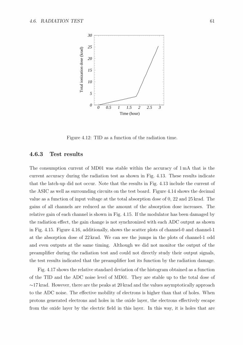
4.6. RADIATION TEST 61
0
5
10
15
20
25
30
0 0.5 1 1.5 2 2.5 3
Tot
al io
niza
tion
dose
(kr
ad)
Time (hour)
Figure 4.12: TID as a function of the radiation time.
4.6.3 Test results
The consumption current of MD01 was stable within the accuracy of 1 mA that is the
current accuracy during the radiation test as shown in Fig. 4.13. These results indicate
that the latch-up did not occur. Note that the results in Fig. 4.13 include the current of
the ASIC as well as surrounding circuits on the test board. Figure 4.14 shows the decimal
value as a function of input voltage at the total absorption dose of 0, 22 and 25 krad. The
gains of all channels are reduced as the amount of the absorption dose increases. The
relative gain of each channel is shown in Fig. 4.15. If the modulator has been damaged by
the radiation effect, the gain change is not synchronized with each ADC output as shown
in Fig. 4.15. Figure 4.16, additionally, shows the scatter plots of channel-0 and channel-1
at the absorption dose of 22 krad. We can see the jumps in the plots of channel-1 odd
and even outputs at the same timing. Although we did not monitor the output of the
preamplifier during the radiation test and could not directly study their output signals,
the test results indicated that the preamplifier lost its function by the radiation damage.
Fig. 4.17 shows the relative standard deviation of the histogram obtained as a function
of the TID and the ADC noise level of MD01. They are stable up to the total dose of
∼17 krad. However, there are the peaks at 20 krad and the values asymptotically approach
to the ADC noise. The effective mobility of electrons is higher than that of holes. When
protons generated electrons and holes in the oxide layer, the electrons effectively escape
from the oxide layer by the electric field in this layer. In this way, it is holes that are
62 CHAPTER 4. PERFORMANCE OF ASICS
trapped in the oxide layer. The trapped holes charge the oxide layer positively, which
leads to the negative threshold voltage shift of MOS FETs and the degradation of 1/f
noise (Yokoyama, M. et al. 2001, Matsushita, T. et al. 1995). The noise increase around
17 krad in Fig. 4.17 can be explained by the effect of the trapped holes. We supposed
the function of the preamplifier gradually degraded and was lost after 20 krad as shown
in Fig. 4.14. Since the preamplifier did not function, the noise from the preamplifier was
removed and the entire ASIC noise approached to the ADC noise.
We investigated the effect of the negative threshold voltage shift of MOS FETs by
the SPICE simulation. Figure 4.18 shows the simulation results with the voltage shift
= 0V (normal condition) and −0.6V. The output of the operational amplifier (OP) with
the voltage shift = 0.6V is not different from that of the normal condition except for the
DC voltage level. The inverter after OP dose not function. Through these results, the
preamplifier malfunctioned in the voltage shift of 0.6 V. However, this inverter is used
in the several circuit blocks such as 5-bit DAC and ∆Σ ADC. Since we think the ADC
properly functions, there is a discrepancy between the test results and the simulation. We
cannot figure out the source of these results from the current data, and will study about
this problem in the next radiation test. The data list that we need to obtain in the next
test are summarized below.
1. Monitor of the preamplifier output : We can directory investigate the total dose
effects of the preamplifier.
2. Data using 5-bit DAC : We did not operate 5-bit DAC in this test. If the preamplifier
malfunctions, we can distinguish which has the problem, the operational amplifier or
the inverter, by the data using 5-bit DAC. The signal of 5-bit DAC is only amplified
by the inverter as shown in Sec. 3.2. If the preamplifier only outputs the 5-bit DAC
signal, the operational amplifier must be damaged.
3. Bitstreams : We should obtain not only filtered ASIC outputs but also bitstreams.
We can study the operation of the ∆Σ ADC during the radiation test from the
patters of the bitstreams.
In Figs. 4.14(b) and 4.17(b), we show the test results of MD01 after annealing at the
room temperature for three months. Since the trapped holes are discharged by the tun-
neling effect during the annealing, we find that the ASIC performance is fully recovered.
We concluded that the ASIC tentatively malfunctions due to high flux of protons. We
think that the radiation tolerance of our ASIC is higher than 17 krad under the practical
proton beam. Figure 4.19 shows the simulation result of the TID in the low earth orbit
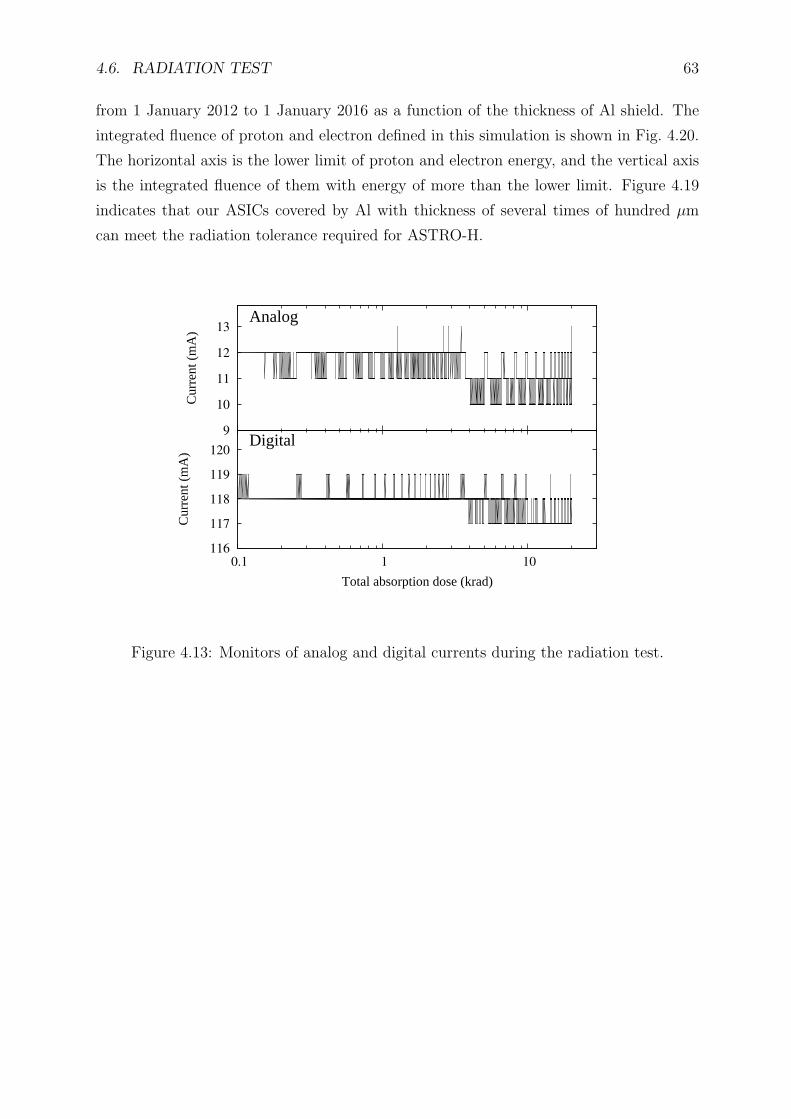
4.6. RADIATION TEST 63
from 1 January 2012 to 1 January 2016 as a function of the thickness of Al shield. The
integrated fluence of proton and electron defined in this simulation is shown in Fig. 4.20.
The horizontal axis is the lower limit of proton and electron energy, and the vertical axis
is the integrated fluence of them with energy of more than the lower limit. Figure 4.19
indicates that our ASICs covered by Al with thickness of several times of hundred µm
can meet the radiation tolerance required for ASTRO-H.
116
117
118
119
120
0.1 1 10
Cur
rent
(m
A)
Total absorption dose (krad)
Digital 9
10
11
12
13
Cur
rent
(m
A)
Analog
Figure 4.13: Monitors of analog and digital currents during the radiation test.
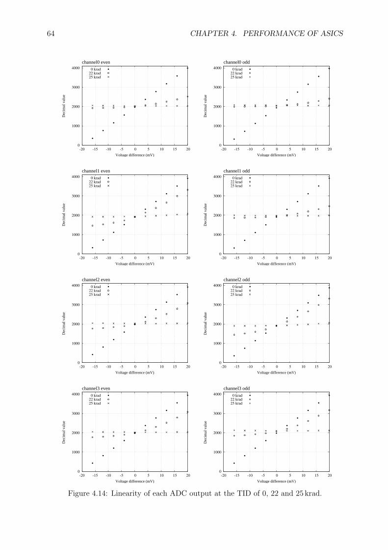
64 CHAPTER 4. PERFORMANCE OF ASICS
0
1000
2000
3000
4000
-20 -15 -10 -5 0 5 10 15 20
Dec
imal
val
ue
Voltage difference (mV)
channel0 even0 krad
22 krad
25 krad
0
1000
2000
3000
4000
-20 -15 -10 -5 0 5 10 15 20
Dec
imal
val
ue
Voltage difference (mV)
channel0 odd0 krad
22 krad
25 krad
0
1000
2000
3000
4000
-20 -15 -10 -5 0 5 10 15 20
Dec
imal
val
ue
Voltage difference (mV)
channel1 even0 krad
22 krad
25 krad
0
1000
2000
3000
4000
-20 -15 -10 -5 0 5 10 15 20
Dec
imal
val
ue
Voltage difference (mV)
channel1 odd0 krad
22 krad
25 krad
0
1000
2000
3000
4000
-20 -15 -10 -5 0 5 10 15 20
Dec
imal
val
ue
Voltage difference (mV)
channel2 even0 krad
22 krad
25 krad
0
1000
2000
3000
4000
-20 -15 -10 -5 0 5 10 15 20
Dec
imal
val
ue
Voltage difference (mV)
channel2 odd0 krad
22 krad
25 krad
0
1000
2000
3000
4000
-20 -15 -10 -5 0 5 10 15 20
Dec
imal
val
ue
Voltage difference (mV)
channel3 even0 krad
22 krad
25 krad
0
1000
2000
3000
4000
-20 -15 -10 -5 0 5 10 15 20
Dec
imal
val
ue
Voltage difference (mV)
channel3 odd0 krad
22 krad
25 krad
Figure 4.14: Linearity of each ADC output at the TID of 0, 22 and 25 krad.
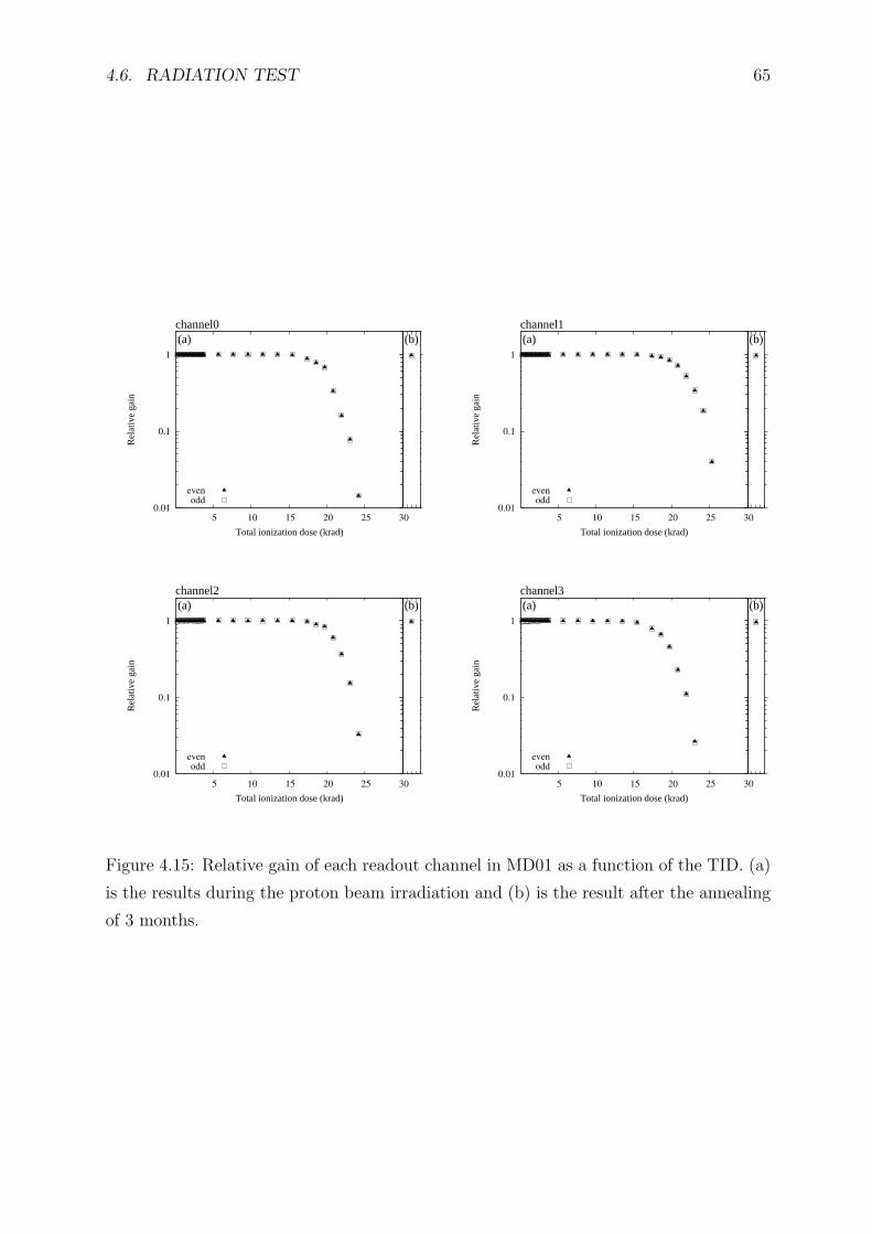
4.6. RADIATION TEST 65
0.01
0.1
1
5 10 15 20 25 30
Rel
ativ
e ga
in
Total ionization dose (krad)
channel0(a)
even
odd
(b)
0.01
0.1
1
5 10 15 20 25 30
Rel
ativ
e ga
in
Total ionization dose (krad)
channel1(a)
even
odd
(b)
0.01
0.1
1
5 10 15 20 25 30
Rel
ativ
e ga
in
Total ionization dose (krad)
channel2(a)
even
odd
(b)
0.01
0.1
1
5 10 15 20 25 30
Rel
ativ
e ga
in
Total ionization dose (krad)
channel3(a)
even
odd
(b)
Figure 4.15: Relative gain of each readout channel in MD01 as a function of the TID. (a)
is the results during the proton beam irradiation and (b) is the result after the annealing
of 3 months.
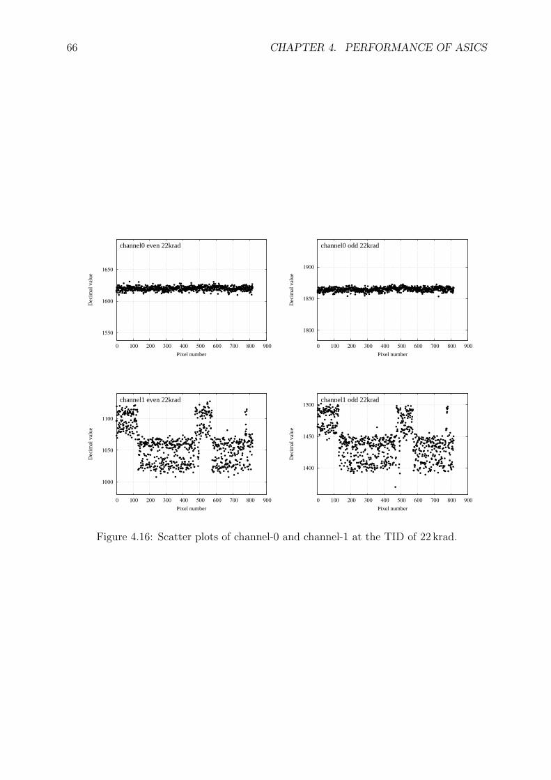
66 CHAPTER 4. PERFORMANCE OF ASICS
1550
1600
1650
0 100 200 300 400 500 600 700 800 900
Dec
imal
val
ue
Pixel number
channel0 even 22krad
1800
1850
1900
0 100 200 300 400 500 600 700 800 900
Dec
imal
val
ue
Pixel number
channel0 odd 22krad
1000
1050
1100
0 100 200 300 400 500 600 700 800 900
Dec
imal
val
ue
Pixel number
channel1 even 22krad
1400
1450
1500
0 100 200 300 400 500 600 700 800 900
Dec
imal
val
ue
Pixel number
channel1 odd 22krad
Figure 4.16: Scatter plots of channel-0 and channel-1 at the TID of 22 krad.
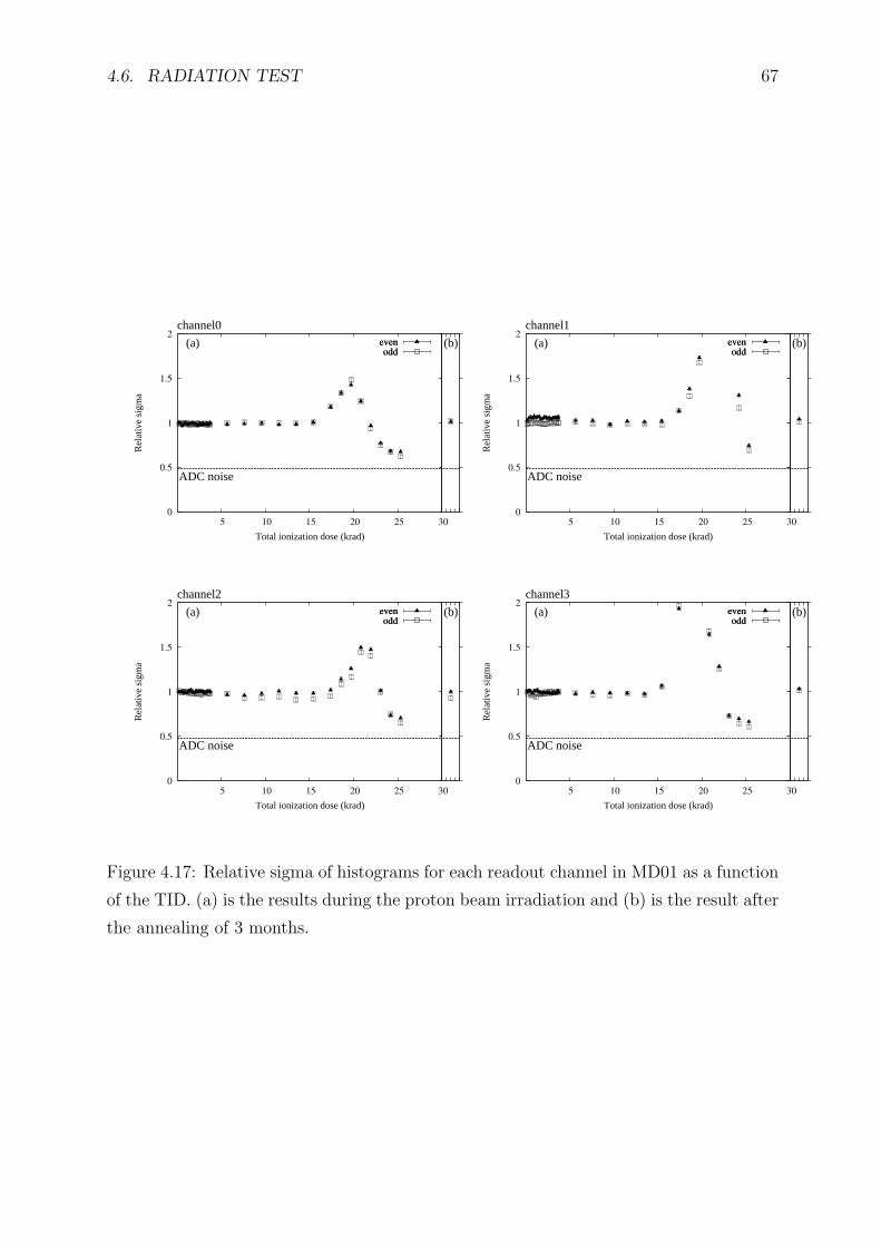
4.6. RADIATION TEST 67
0
0.5
1
1.5
2
5 10 15 20 25 30
Rel
ativ
e si
gma
Total ionization dose (krad)
channel0
(a)
ADC noise
even
odd(b)even
odd
0
0.5
1
1.5
2
5 10 15 20 25 30
Rel
ativ
e si
gma
Total ionization dose (krad)
channel1
(a)
ADC noise
even
odd(b)even
odd
0
0.5
1
1.5
2
5 10 15 20 25 30
Rel
ativ
e si
gma
Total ionization dose (krad)
channel2
(a)
ADC noise
even
odd(b)even
odd
0
0.5
1
1.5
2
5 10 15 20 25 30
Rel
ativ
e si
gma
Total ionization dose (krad)
channel3
(a)
ADC noise
even
odd(b)even
odd
Figure 4.17: Relative sigma of histograms for each readout channel in MD01 as a function
of the TID. (a) is the results during the proton beam irradiation and (b) is the result after
the annealing of 3 months.
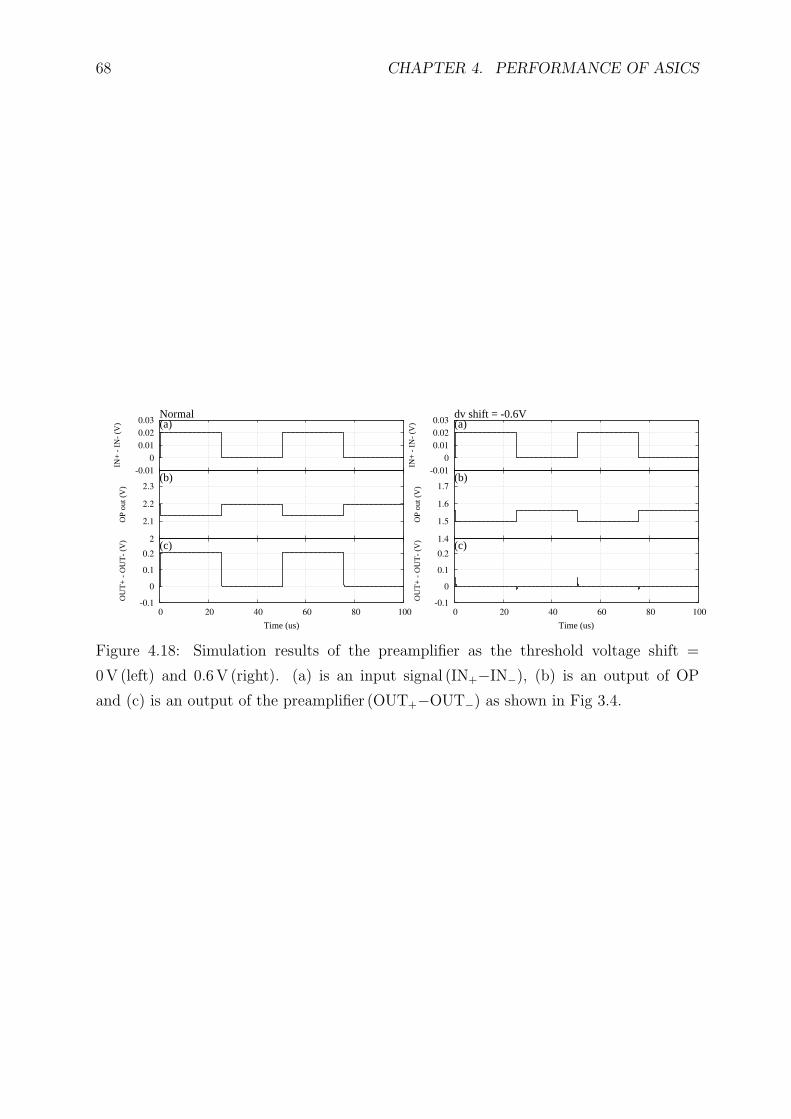
68 CHAPTER 4. PERFORMANCE OF ASICS
-0.1
0
0.1
0.2
0 20 40 60 80 100
OU
T+
- O
UT
- (V
)
Time (us)
(c) 2
2.1
2.2
2.3
OP
out (
V)
(b)-0.01
0
0.01
0.02
0.03
IN+
- I
N-
(V)
Normal(a)
-0.1
0
0.1
0.2
0 20 40 60 80 100
OU
T+
- O
UT
- (V
)
Time (us)
(c) 1.4
1.5
1.6
1.7
OP
out (
V)
(b)-0.01
0
0.01
0.02
0.03
IN+
- I
N-
(V)
dv shift = -0.6V(a)
Figure 4.18: Simulation results of the preamplifier as the threshold voltage shift =
0 V (left) and 0.6 V (right). (a) is an input signal (IN+−IN−), (b) is an output of OP
and (c) is an output of the preamplifier (OUT+−OUT−) as shown in Fig 3.4.
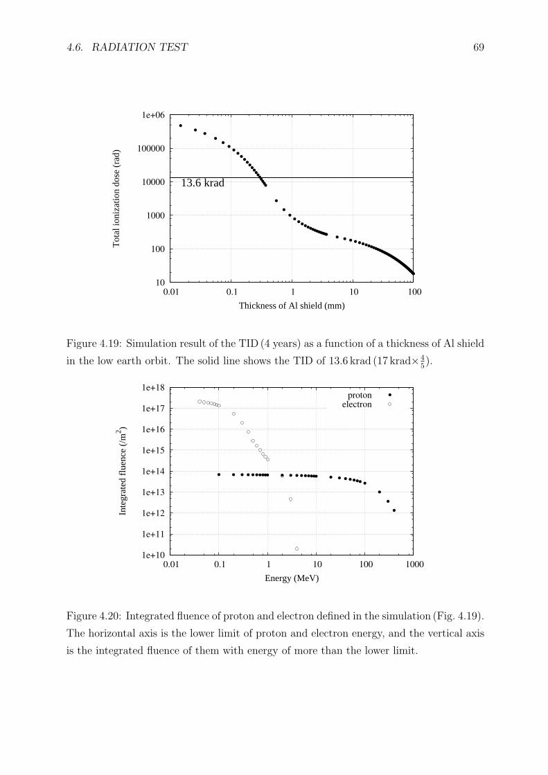
4.6. RADIATION TEST 69
10
100
1000
10000
100000
1e+06
0.01 0.1 1 10 100
Tot
al io
niza
tion
dose
(ra
d)
Thickness of Al shield (mm)
13.6 krad
Figure 4.19: Simulation result of the TID (4 years) as a function of a thickness of Al shield
in the low earth orbit. The solid line shows the TID of 13.6 krad (17 krad×45).
1e+10
1e+11
1e+12
1e+13
1e+14
1e+15
1e+16
1e+17
1e+18
0.01 0.1 1 10 100 1000
Inte
grat
ed f
luen
ce (
/m2 )
Energy (MeV)
protonelectron
Figure 4.20: Integrated fluence of proton and electron defined in the simulation (Fig. 4.19).
The horizontal axis is the lower limit of proton and electron energy, and the vertical axis
is the integrated fluence of them with energy of more than the lower limit.
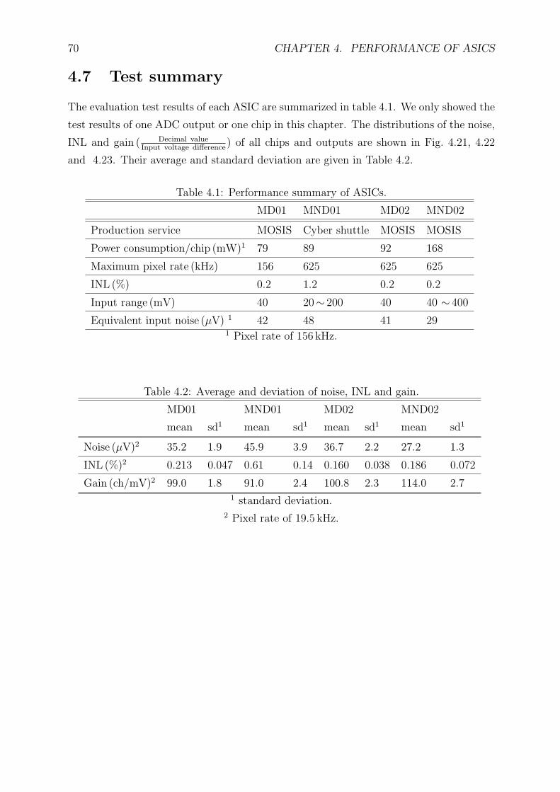
70 CHAPTER 4. PERFORMANCE OF ASICS
4.7 Test summary
The evaluation test results of each ASIC are summarized in table 4.1. We only showed the
test results of one ADC output or one chip in this chapter. The distributions of the noise,
INL and gain ( Decimal valueInput voltage difference
) of all chips and outputs are shown in Fig. 4.21, 4.22
and 4.23. Their average and standard deviation are given in Table 4.2.
Table 4.1: Performance summary of ASICs.
MD01 MND01 MD02 MND02
Production service MOSIS Cyber shuttle MOSIS MOSIS
Power consumption/chip (mW)1 79 89 92 168
Maximum pixel rate (kHz) 156 625 625 625
INL (%) 0.2 1.2 0.2 0.2
Input range (mV) 40 20∼ 200 40 40 ∼ 400
Equivalent input noise (µV) 1 42 48 41 291 Pixel rate of 156 kHz.
Table 4.2: Average and deviation of noise, INL and gain.
MD01 MND01 MD02 MND02
mean sd1 mean sd1 mean sd1 mean sd1
Noise (µV)2 35.2 1.9 45.9 3.9 36.7 2.2 27.2 1.3
INL (%)2 0.213 0.047 0.61 0.14 0.160 0.038 0.186 0.072
Gain (ch/mV)2 99.0 1.8 91.0 2.4 100.8 2.3 114.0 2.71 standard deviation.
2 Pixel rate of 19.5 kHz.
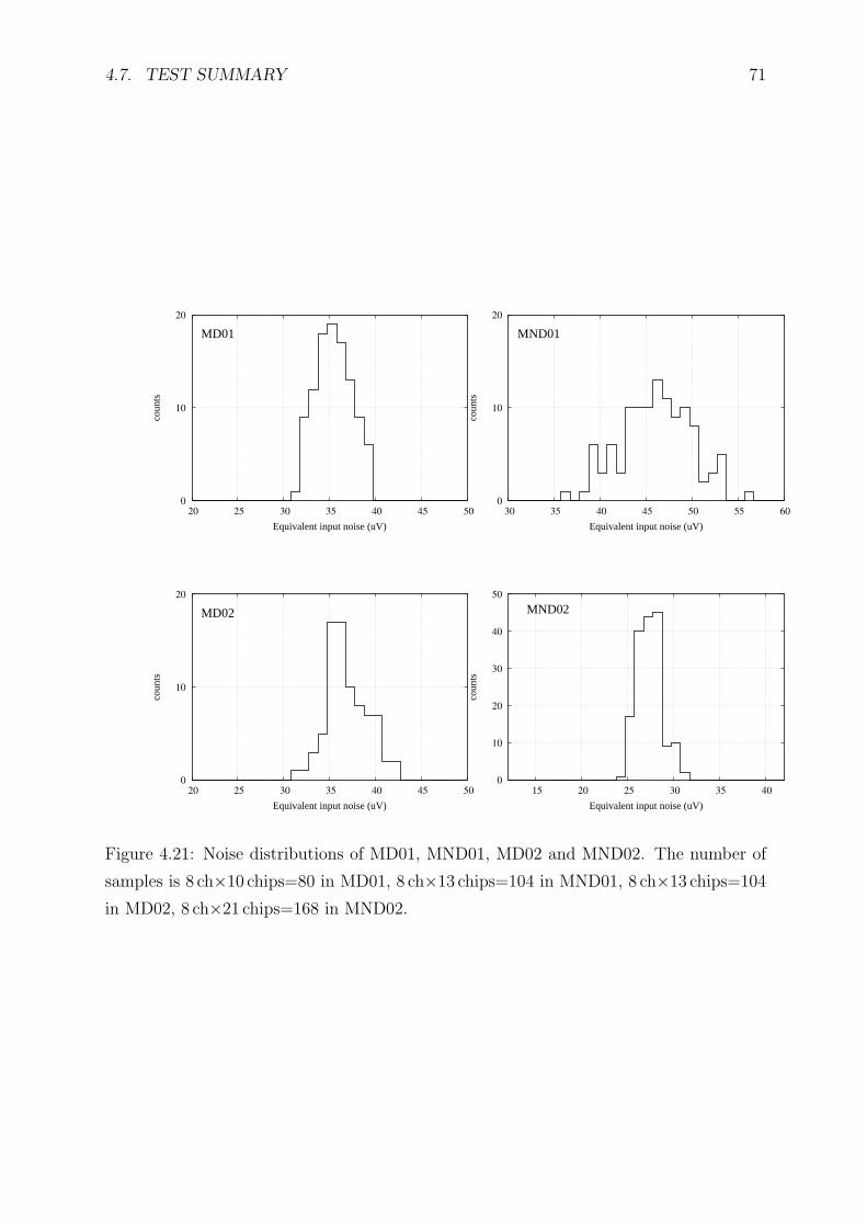
4.7. TEST SUMMARY 71
0
10
20
20 25 30 35 40 45 50
coun
ts
Equivalent input noise (uV)
MD01
0
10
20
30 35 40 45 50 55 60
coun
ts
Equivalent input noise (uV)
MND01
0
10
20
20 25 30 35 40 45 50
coun
ts
Equivalent input noise (uV)
MD02
0
10
20
30
40
50
15 20 25 30 35 40
coun
ts
Equivalent input noise (uV)
MND02
Figure 4.21: Noise distributions of MD01, MND01, MD02 and MND02. The number of
samples is 8 ch×10 chips=80 in MD01, 8 ch×13 chips=104 in MND01, 8 ch×13 chips=104
in MD02, 8 ch×21 chips=168 in MND02.
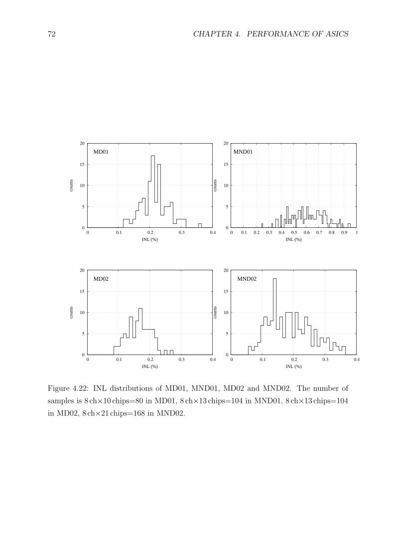
72 CHAPTER 4. PERFORMANCE OF ASICS
0
5
10
15
20
0 0.1 0.2 0.3 0.4
coun
ts
INL (%)
MD01
0
5
10
15
20
0 0.1 0.2 0.3 0.4 0.5 0.6 0.7 0.8 0.9 1
coun
ts
INL (%)
MND01
0
5
10
15
20
0 0.1 0.2 0.3 0.4
coun
ts
INL (%)
MD02
0
5
10
15
20
0 0.1 0.2 0.3 0.4
coun
ts
INL (%)
MND02
Figure 4.22: INL distributions of MD01, MND01, MD02 and MND02. The number of
samples is 8 ch×10 chips=80 in MD01, 8 ch×13 chips=104 in MND01, 8 ch×13 chips=104
in MD02, 8 ch×21 chips=168 in MND02.
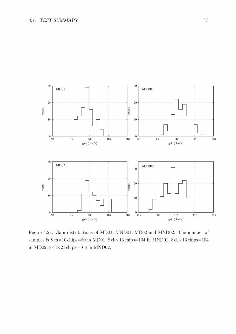
4.7. TEST SUMMARY 73
0
10
20
30
90 95 100 105 110
coun
ts
gain (ch/mV)
MD01
0
10
20
30
80 85 90 95 100
coun
ts
gain (ch/mV)
MND01
0
10
20
30
90 95 100 105 110
coun
ts
gain (ch/mV)
MD02
0
10
20
30
105 110 115 120 125
coun
ts
gain (ch/mV)
MND02
Figure 4.23: Gain distributions of MD01, MND01, MD02 and MND02. The number of
samples is 8 ch×10 chips=80 in MD01, 8 ch×13 chips=104 in MND01, 8 ch×13 chips=104
in MD02, 8 ch×21 chips=168 in MND02.

Chapter 5
Performance of CCD camera
systems using ASICs
5.1 Evaluation test setup
We confirmed that ASICs properly worked as we designed in the evaluation test us-
ing the pseudo signals. For the next step, we tested the readout of X-ray CCDs using
MD01. The block diagram of the test system is shown in Fig. 5.1. The control signals
for the ASIC and the drive signals for the CCD are provided by MiKE system shown in
Fig. 5.2 (left) (Miyata, E. et al. 2001). MiKE system is the CCD test system developed in
our laboratory. It provides 16 analog signals and 10 digital signals. The output range of
analog signal is ±12V with resolution of 8-bit and the maximum toggle frequency of the
signals is 7 MHz, which meets the requirement for the operation of wide variety of CCDs.
The high DC voltages, over ±12V, for OD (the drain voltage used in an FDA) and the
backside charging are given by other power supply units.
The analog and digital signals are generated by the signal pattern data loaded from
the DP. The DP shown in Fig. 5.2 (right) consists of the CPU board (Armadillo-9) and
the FPGA board. The former is a commercial product of Atmark Techno, Inc. and
the latter is developed in our laboratory. The FPGA board is connected to the CPU
board through PC/104 bus. Since the ASICs do not include the decimation filter as
described in Sec. 3.4.2, we implemented the function in the FPGA and the filtered data
were transmitted to the CPU board through PC/104 bus. The CPU board does not have
a large memory enough to accept many CCD frame data. The CCD data are written to
the hard disc drive (HDD) through network. MiKE system includes the readout system
of CCD signals which consists of an iCDS circuit and ADC. Its noise level including
CCD is 5 electrons and the energy resolution (FWHM) achieves 132±2 eV as shown in
75
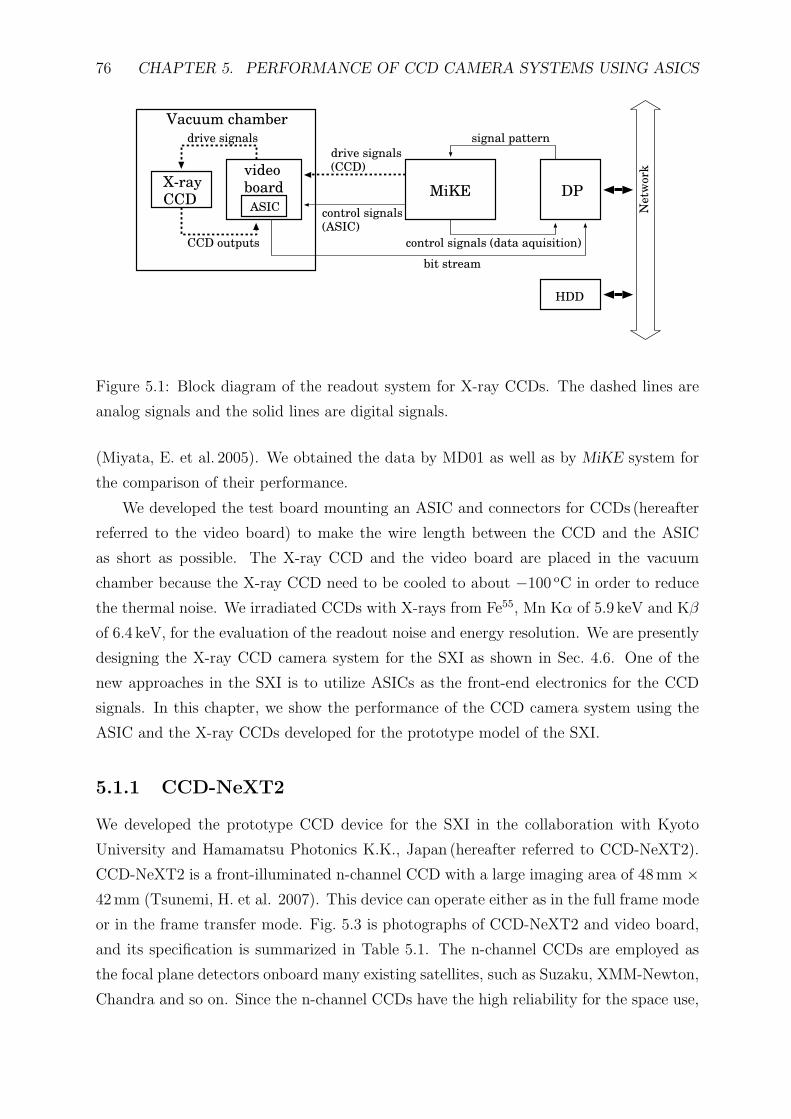
76 CHAPTER 5. PERFORMANCE OF CCD CAMERA SYSTEMS USING ASICS
X-rayCCD
videoboard
Vacuum chamber
MiKE DP
drive signals
CCD outputs
drive signals(CCD)
control signals(ASIC)
bit stream
signal pattern
control signals (data aquisition)
Netw
ork
HDD
ASIC
Figure 5.1: Block diagram of the readout system for X-ray CCDs. The dashed lines are
analog signals and the solid lines are digital signals.
(Miyata, E. et al. 2005). We obtained the data by MD01 as well as by MiKE system for
the comparison of their performance.
We developed the test board mounting an ASIC and connectors for CCDs (hereafter
referred to the video board) to make the wire length between the CCD and the ASIC
as short as possible. The X-ray CCD and the video board are placed in the vacuum
chamber because the X-ray CCD need to be cooled to about −100 oC in order to reduce
the thermal noise. We irradiated CCDs with X-rays from Fe55, Mn Kα of 5.9 keV and Kβ
of 6.4 keV, for the evaluation of the readout noise and energy resolution. We are presently
designing the X-ray CCD camera system for the SXI as shown in Sec. 4.6. One of the
new approaches in the SXI is to utilize ASICs as the front-end electronics for the CCD
signals. In this chapter, we show the performance of the CCD camera system using the
ASIC and the X-ray CCDs developed for the prototype model of the SXI.
5.1.1 CCD-NeXT2
We developed the prototype CCD device for the SXI in the collaboration with Kyoto
University and Hamamatsu Photonics K.K., Japan (hereafter referred to CCD-NeXT2).
CCD-NeXT2 is a front-illuminated n-channel CCD with a large imaging area of 48mm ×42 mm (Tsunemi, H. et al. 2007). This device can operate either as in the full frame mode
or in the frame transfer mode. Fig. 5.3 is photographs of CCD-NeXT2 and video board,
and its specification is summarized in Table 5.1. The n-channel CCDs are employed as
the focal plane detectors onboard many existing satellites, such as Suzaku, XMM-Newton,
Chandra and so on. Since the n-channel CCDs have the high reliability for the space use,
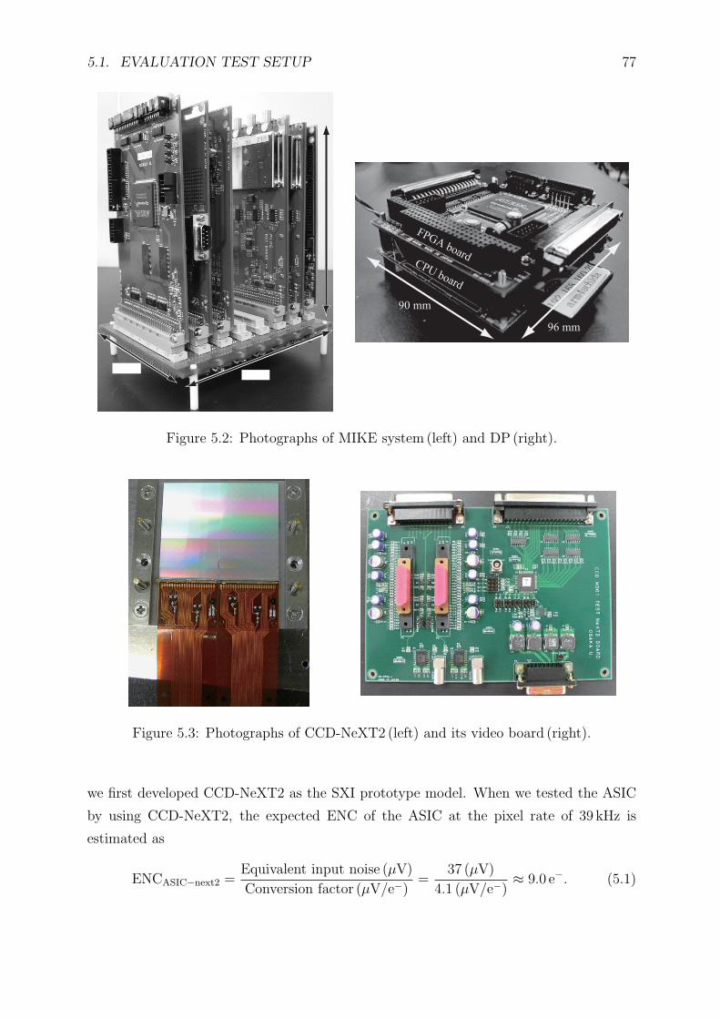
5.1. EVALUATION TEST SETUP 77
160mm
130mm160mm
90 mm
96 mm
FPGA boardCPU board
Figure 5.2: Photographs of MIKE system (left) and DP (right).
Figure 5.3: Photographs of CCD-NeXT2 (left) and its video board (right).
we first developed CCD-NeXT2 as the SXI prototype model. When we tested the ASIC
by using CCD-NeXT2, the expected ENC of the ASIC at the pixel rate of 39 kHz is
estimated as
ENCASIC−next2 =Equivalent input noise (µV)
Conversion factor (µV/e−)=
37 (µV)
4.1 (µV/e−)≈ 9.0 e−. (5.1)
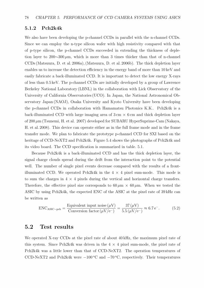
78 CHAPTER 5. PERFORMANCE OF CCD CAMERA SYSTEMS USING ASICS
5.1.2 Pch2k4k
We also have been developing the p-channel CCDs in parallel with the n-channel CCDs.
Since we can employ the n-type silicon wafer with high resistivity compared with that
of p-type silicon, the p-channel CCDs succeeded in extending the thickness of deple-
tion layer to 200∼300µm, which is more than 3 times thicker than that of n-channel
CCDs (Matsuura, D. et al. 2006a), (Matsuura, D. et al. 2006b). The thick depletion layer
enables us to increase the detection efficiency in the energy band of more than 10 keV and
easily fabricate a back-illuminated CCD. It is important to detect the low energy X-rays
of less than 0.5 keV. The p-channel CCDs are initially developed by a group of Lawrence
Berkeley National Laboratory (LBNL) in the collaboration with Lick Observatory of the
University of California Observatories (UCO). In Japan, the National Astronomical Ob-
servatory Japan (NAOJ), Osaka University and Kyoto University have been developing
the p-channel CCDs in collaboration with Hamamatsu Photonics K.K.. Pch2k4k is a
back-illuminated CCD with large imaging area of 3 cm × 6 cm and thick depletion layer
of 200µm(Tsunemi, H. et al. 2007) developed for SUBARU HyperSuprime-Cam (Nakaya,
H. et al. 2008). This device can operate either as in the full frame mode and in the frame
transfer mode. We plan to fabricate the prototype p-channel CCD for SXI based on the
heritage of CCD-NeXT2 and Pch2k4k. Figure 5.4 shows the photographs of Pch2k4k and
its video board. The CCD specification is summarized in table. 5.1.
Because Pch2k4k is a back-illuminated CCD and has the thick depletion layer, the
signal charge clouds spread during the drift from the interaction point to the potential
well. The number of single pixel events decrease compared with the results of a front-
illuminated CCD. We operated Pch2k4k in the 4 × 4 pixel sum-mode. This mode is
to sum the charges in 4 × 4 pixels during the vertical and horizontal charge transfers.
Therefore, the effective pixel size corresponds to 60µm × 60µm. When we tested the
ASIC by using Pch2k4k, the expected ENC of the ASIC at the pixel rate of 39 kHz can
be written as
ENCASIC−pch =Equivalent input noise (µV)
Conversion factor (µV/e−)=
37 (µV)
5.5 (µV/e−)≈ 6.7 e−. (5.2)
5.2 Test results
We operated X-ray CCDs at the pixel rate of about 40 kHz, the maximum pixel rate of
this system. Since Pch2k4k was driven in the 4 × 4 pixel sum-mode, the pixel rate of
Pch2k4k was a little lower than that of CCD-NeXT2. The operation temperatures of
CCD-NeXT2 and Pch2k4k were −100 oC and −70 oC, respectively. Their temperatures
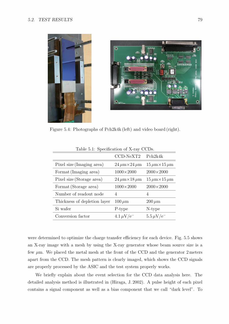
5.2. TEST RESULTS 79
Figure 5.4: Photographs of Pch2k4k (left) and video board (right).
Table 5.1: Specification of X-ray CCDs.
CCD-NeXT2 Pch2k4k
Pixel size (Imaging area) 24µm×24µm 15µm×15µm
Format (Imaging area) 1000×2000 2000×2000
Pixel size (Storage area) 24µm×18µm 15µm×15µm
Format (Storage area) 1000×2000 2000×2000
Number of readout node 4 4
Thickness of depletion layer 100µm 200µm
Si wafer P-type N-type
Conversion factor 4.1µV/e− 5.5µV/e−
were determined to optimize the charge transfer efficiency for each device. Fig. 5.5 shows
an X-ray image with a mesh by using the X-ray generator whose beam source size is a
few µm. We placed the metal mesh at the front of the CCD and the generator 2meters
apart from the CCD. The mesh pattern is clearly imaged, which shows the CCD signals
are properly processed by the ASIC and the test system properly works.
We briefly explain about the event selection for the CCD data analysis here. The
detailed analysis method is illustrated in (Hiraga, J. 2002). A pulse height of each pixel
contains a signal component as well as a bias component that we call “dark level”. To

80 CHAPTER 5. PERFORMANCE OF CCD CAMERA SYSTEMS USING ASICS
extract the signal component, we first determine the dark level of each pixel and subtract
that from the pulse height. The dark level is the averaged pixel level of 32 frames in
this analysis. The charge cloud splits into adjacent pixels when the interaction occurs
at the pixel boundary. We determine the threshold, which we call “split threshold”, to
distinguish whether the relevant pixel is the split one or the dark noise. We set the split
threshold to 3 sigma of the readout noise level in this chapter. We should select only single
pixel events to achieve the high energy resolution. However, we use a part of the split
events to improve the detection efficiency. ASCA grades (A. Yamashita, A. et al. 1997) is
employed to separate the events into 8 patterns (g0∼g7), g0 is a single event and g1∼g7
are split events. In XIS, the spectrum is created by using g0,2,3,4 and 6 events.
Figures 5.6∼ 5.8 show the spectra of 55Fe using g0 and g02346 events obtained by
CCD-NeXT2 and Pch2k4k, respectively. Note that the pixel data of odd and even columns
are processed by separate ADCs, odd and even ADCs. The standard deviation of the ADC
gain in MD01 is 1.8 (ch/mV) as shown in Table 4.2. We compensated the difference of the
ADC gain to prevent the degradation of energy resolution before the data combine. Two
emission lines, Mn Kα (5.9 keV) and Kβ (6.5 keV), are clearly seen and the low energy tail
of each peak is not found in these spectra. We fitted each line with a Gaussian function
and a constant to evaluate energy resolution.
Readout noise
The readout noise each channel is shown in Tables 5.2 and 5.4. The noise of channel3 is
worse than those of other channels by 30∼100%, which is a little larger than the noise
distribution of MD01 shown in Fig. 4.21. Tables 5.3 and 5.5 exhibit the test results
of MiKE system by using the same CCD devices. The noise level of channel3 shows no
significant difference compared with other channels. Since the noise of CCDs and ASICs
are proper from the test results, we suppose that the layout design of the video boards,
especially for the analog line between the ASIC and CCD, leads to the noise degradation
of channel3. We excluded the data of channel3 in the calculation of the averaged readout
noise and energy resolution. The averaged readout noises of Channel0∼Channel2 for
CCD-NeXT2 and Pch2k4k are 9.8 e− and 7.5 e−, respectively. The expected noise from the
ASIC is 9.0 e− in eq. 5.1 when we use CCD-NeXT2. The residual between the measured
noise and the calculated one of the ASIC corresponds to the noise component from CCD-
NeXT2. The noise from CCD-NeXT2 is given as
ENCnext2 =√
(9.8 e−)2 − (9.0 e−)2 ≈ 3.9 e−. (5.3)
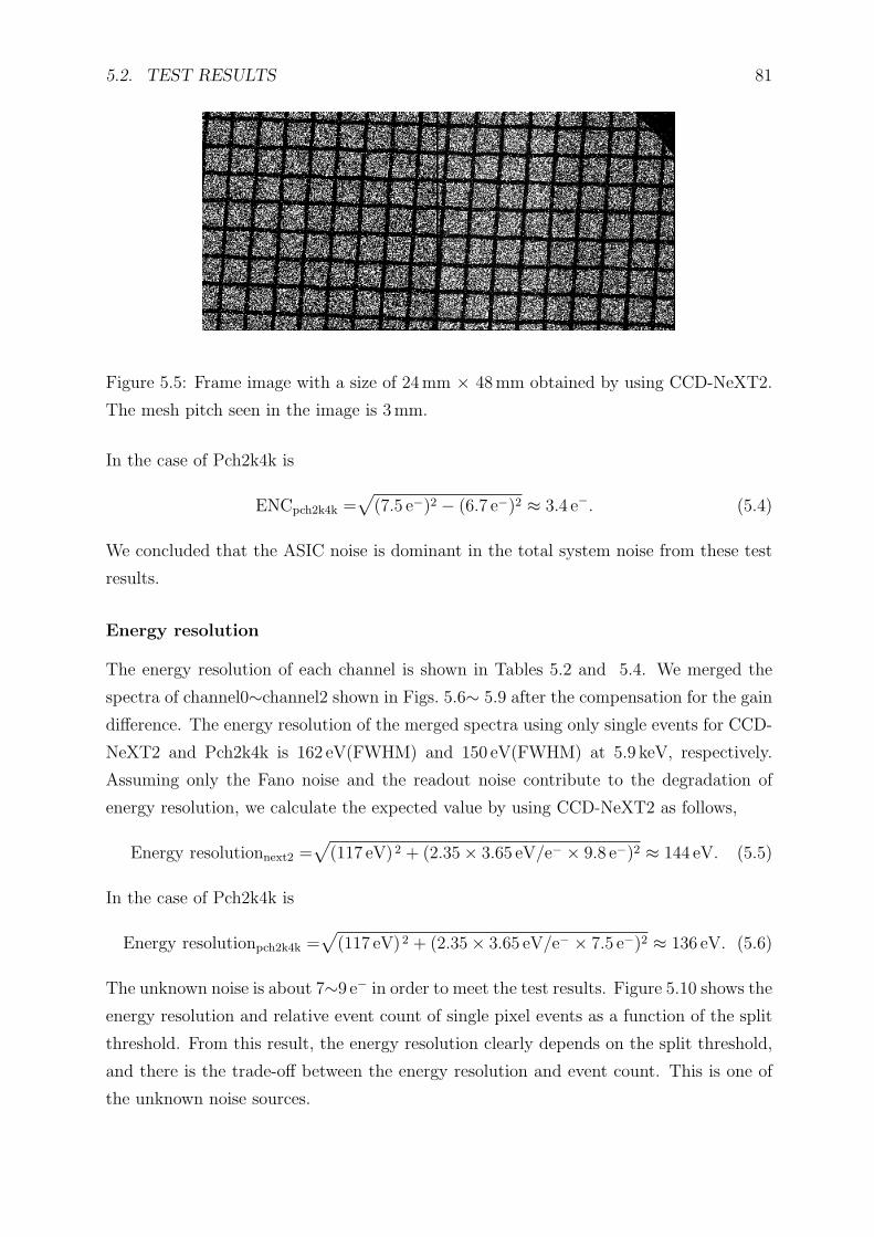
5.2. TEST RESULTS 81
Figure 5.5: Frame image with a size of 24mm × 48mm obtained by using CCD-NeXT2.
The mesh pitch seen in the image is 3 mm.
In the case of Pch2k4k is
ENCpch2k4k =√
(7.5 e−)2 − (6.7 e−)2 ≈ 3.4 e−. (5.4)
We concluded that the ASIC noise is dominant in the total system noise from these test
results.
Energy resolution
The energy resolution of each channel is shown in Tables 5.2 and 5.4. We merged the
spectra of channel0∼channel2 shown in Figs. 5.6∼ 5.9 after the compensation for the gain
difference. The energy resolution of the merged spectra using only single events for CCD-
NeXT2 and Pch2k4k is 162 eV(FWHM) and 150 eV(FWHM) at 5.9 keV, respectively.
Assuming only the Fano noise and the readout noise contribute to the degradation of
energy resolution, we calculate the expected value by using CCD-NeXT2 as follows,
Energy resolutionnext2 =√
(117 eV) 2 + (2.35 × 3.65 eV/e− × 9.8 e−)2 ≈ 144 eV. (5.5)
In the case of Pch2k4k is
Energy resolutionpch2k4k =√
(117 eV) 2 + (2.35 × 3.65 eV/e− × 7.5 e−)2 ≈ 136 eV. (5.6)
The unknown noise is about 7∼9 e− in order to meet the test results. Figure 5.10 shows the
energy resolution and relative event count of single pixel events as a function of the split
threshold. From this result, the energy resolution clearly depends on the split threshold,
and there is the trade-off between the energy resolution and event count. This is one of
the unknown noise sources.
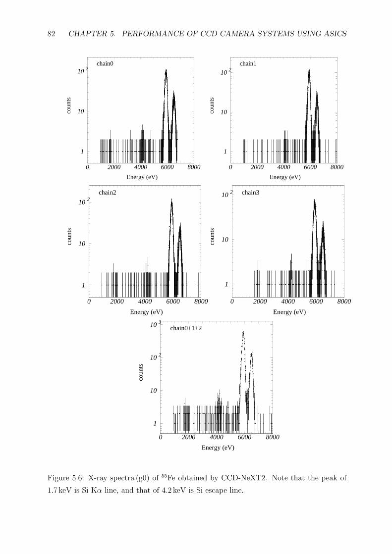
82 CHAPTER 5. PERFORMANCE OF CCD CAMERA SYSTEMS USING ASICS
1
10
10 2
0 2000 4000 6000 8000
coun
ts
Energy (eV)
chain0
1
10
10 2
0 2000 4000 6000 8000
coun
ts
Energy (eV)
chain1
1
10
10 2
0 2000 4000 6000 8000
coun
ts
Energy (eV)
chain2
1
10
10 2
0 2000 4000 6000 8000
coun
ts
Energy (eV)
chain3
1
10
10 2
10 3
0 2000 4000 6000 8000
coun
ts
Energy (eV)
chain0+1+2
Figure 5.6: X-ray spectra (g0) of 55Fe obtained by CCD-NeXT2. Note that the peak of
1.7 keV is Si Kα line, and that of 4.2 keV is Si escape line.
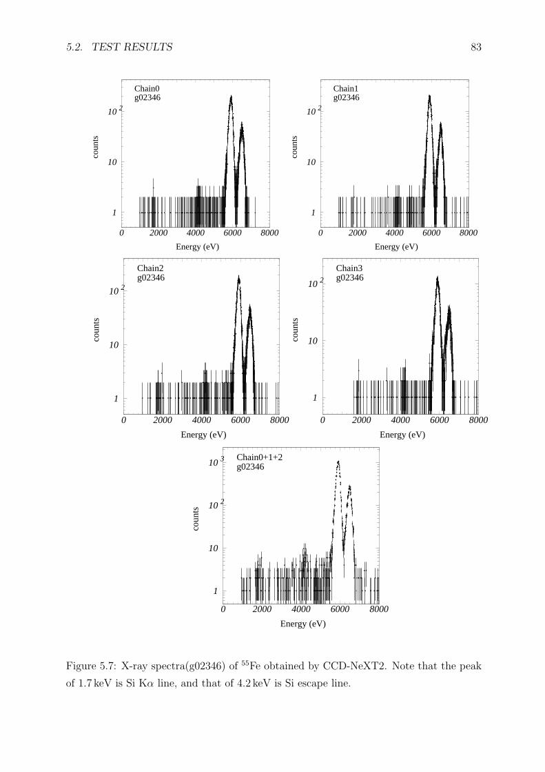
5.2. TEST RESULTS 83
1
10
10 2
0 2000 4000 6000 8000
coun
ts
Energy (eV)
g02346Chain0
1
10
10 2
0 2000 4000 6000 8000
coun
ts
Energy (eV)
g02346Chain1
1
10
10 2
0 2000 4000 6000 8000
coun
ts
Energy (eV)
g02346Chain2
1
10
10 2
0 2000 4000 6000 8000
coun
ts
Energy (eV)
g02346Chain3
1
10
10 2
10 3
0 2000 4000 6000 8000
coun
ts
Energy (eV)
Chain0+1+2g02346
Figure 5.7: X-ray spectra(g02346) of 55Fe obtained by CCD-NeXT2. Note that the peak
of 1.7 keV is Si Kα line, and that of 4.2 keV is Si escape line.
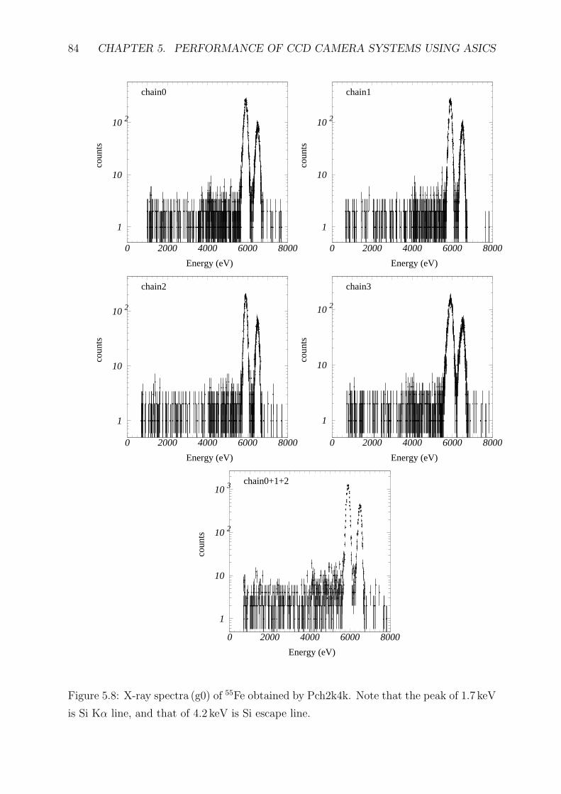
84 CHAPTER 5. PERFORMANCE OF CCD CAMERA SYSTEMS USING ASICS
1
10
10 2
0 2000 4000 6000 8000
coun
ts
Energy (eV)
chain0
1
10
10 2
0 2000 4000 6000 8000
coun
ts
Energy (eV)
chain1
1
10
10 2
0 2000 4000 6000 8000
coun
ts
Energy (eV)
chain2
1
10
10 2
0 2000 4000 6000 8000
coun
ts
Energy (eV)
chain3
1
10
10 2
10 3
0 2000 4000 6000 8000
coun
ts
Energy (eV)
chain0+1+2
Figure 5.8: X-ray spectra (g0) of 55Fe obtained by Pch2k4k. Note that the peak of 1.7 keV
is Si Kα line, and that of 4.2 keV is Si escape line.
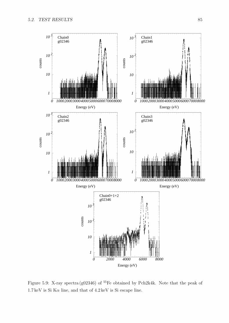
5.2. TEST RESULTS 85
1
10
10 2
10 3
0 10002000300040005000600070008000
coun
ts
Energy (eV)
g02346Chain0
1
10
10 2
10 3
0 10002000300040005000600070008000
coun
ts
Energy (eV)
g02346Chain1
1
10
10 2
10 3
0 10002000300040005000600070008000
coun
ts
Energy (eV)
g02346Chain2
1
10
10 2
0 10002000300040005000600070008000
coun
ts
Energy (eV)
g02346Chain3
1
10
10 2
10 3
0 2000 4000 6000 8000
coun
ts
Energy (eV)
g02346Chain0+1+2
Figure 5.9: X-ray spectra (g02346) of 55Fe obtained by Pch2k4k. Note that the peak of
1.7 keV is Si Kα line, and that of 4.2 keV is Si escape line.
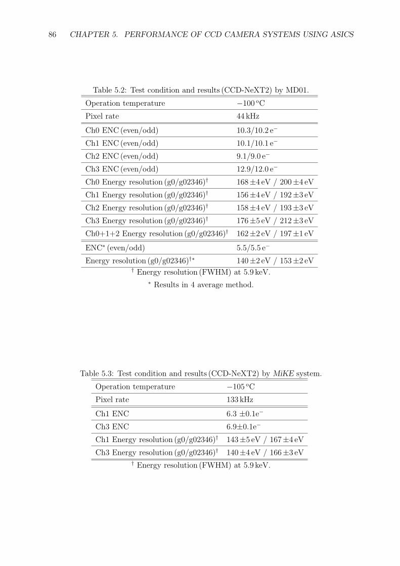
86 CHAPTER 5. PERFORMANCE OF CCD CAMERA SYSTEMS USING ASICS
Table 5.2: Test condition and results (CCD-NeXT2) by MD01.
Operation temperature −100 oC
Pixel rate 44 kHz
Ch0 ENC (even/odd) 10.3/10.2 e−
Ch1 ENC (even/odd) 10.1/10.1 e−
Ch2 ENC (even/odd) 9.1/9.0 e−
Ch3 ENC (even/odd) 12.9/12.0 e−
Ch0 Energy resolution (g0/g02346)† 168±4 eV / 200±4 eV
Ch1 Energy resolution (g0/g02346)† 156±4 eV / 192±3 eV
Ch2 Energy resolution (g0/g02346)† 158±4 eV / 193±3 eV
Ch3 Energy resolution (g0/g02346)† 176±5 eV / 212±3 eV
Ch0+1+2 Energy resolution (g0/g02346)† 162±2 eV / 197±1 eV
ENC∗ (even/odd) 5.5/5.5 e−
Energy resolution (g0/g02346)†∗ 140±2 eV / 153±2 eV† Energy resolution (FWHM) at 5.9 keV.
∗ Results in 4 average method.
Table 5.3: Test condition and results (CCD-NeXT2) by MiKE system.
Operation temperature −105 oC
Pixel rate 133 kHz
Ch1 ENC 6.3 ±0.1e−
Ch3 ENC 6.9±0.1e−
Ch1 Energy resolution (g0/g02346)† 143±5 eV / 167±4 eV
Ch3 Energy resolution (g0/g02346)† 140±4 eV / 166±3 eV† Energy resolution (FWHM) at 5.9 keV.
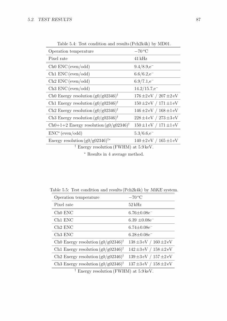
5.2. TEST RESULTS 87
Table 5.4: Test condition and results (Pch2k4k) by MD01.
Operation temperature −70 oC
Pixel rate 41 kHz
Ch0 ENC (even/odd) 9.4/8.9,e−
Ch1 ENC (even/odd) 6.6/6.2,e−
Ch2 ENC (even/odd) 6.9/7.1,e−
Ch3 ENC (even/odd) 14.2/15.7,e−
Ch0 Energy resolution (g0/g02346)† 176±2 eV / 207±2 eV
Ch1 Energy resolution (g0/g02346)† 150±2 eV / 171±1 eV
Ch2 Energy resolution (g0/g02346)† 146±2 eV / 168±1 eV
Ch3 Energy resolution (g0/g02346)† 228±4 eV / 273±3 eV
Ch0+1+2 Energy resolution (g0/g02346)† 150±1 eV / 171±1 eV
ENC∗ (even/odd) 5.3/6.6,e−
Energy resolution (g0/g02346)†∗ 140±2 eV / 165±1 eV† Energy resolution (FWHM) at 5.9 keV.
∗ Results in 4 average method.
Table 5.5: Test condition and results (Pch2k4k) by MiKE system.
Operation temperature −70 oC
Pixel rate 52 kHz
Ch0 ENC 6.76±0.08e−
Ch1 ENC 6.39 ±0.08e−
Ch2 ENC 6.74±0.08e−
Ch3 ENC 6.28±0.08e−
Ch0 Energy resolution (g0/g02346)† 138±3 eV / 160±2 eV
Ch1 Energy resolution (g0/g02346)† 142±3 eV / 158±2 eV
Ch2 Energy resolution (g0/g02346)† 139±3 eV / 157±2 eV
Ch3 Energy resolution (g0/g02346)† 137±3 eV / 158±2 eV† Energy resolution (FWHM) at 5.9 keV.
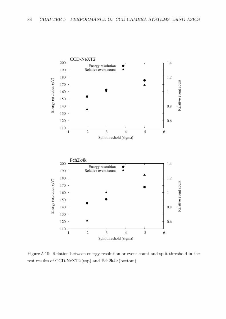
88 CHAPTER 5. PERFORMANCE OF CCD CAMERA SYSTEMS USING ASICS
110
120
130
140
150
160
170
180
190
200
1 2 3 4 5 6
0.6
0.8
1
1.2
1.4
Ene
rgy
reso
lutio
n (e
V)
Rel
ativ
e ev
ent c
ount
Split threshold (sigma)
CCD-NeXT2Energy resolution
Relative event count
110
120
130
140
150
160
170
180
190
200
1 2 3 4 5 6
0.6
0.8
1
1.2
1.4
Ene
rgy
reso
lutio
n (e
V)
Ral
ativ
e ev
ent c
ount
Split threshold (sigma)
Pch2k4kEnergy resoultion
Relative event count
Figure 5.10: Relation between energy resolution or event count and split threshold in the
test results of CCD-NeXT2 (top) and Pch2k4k (bottom).
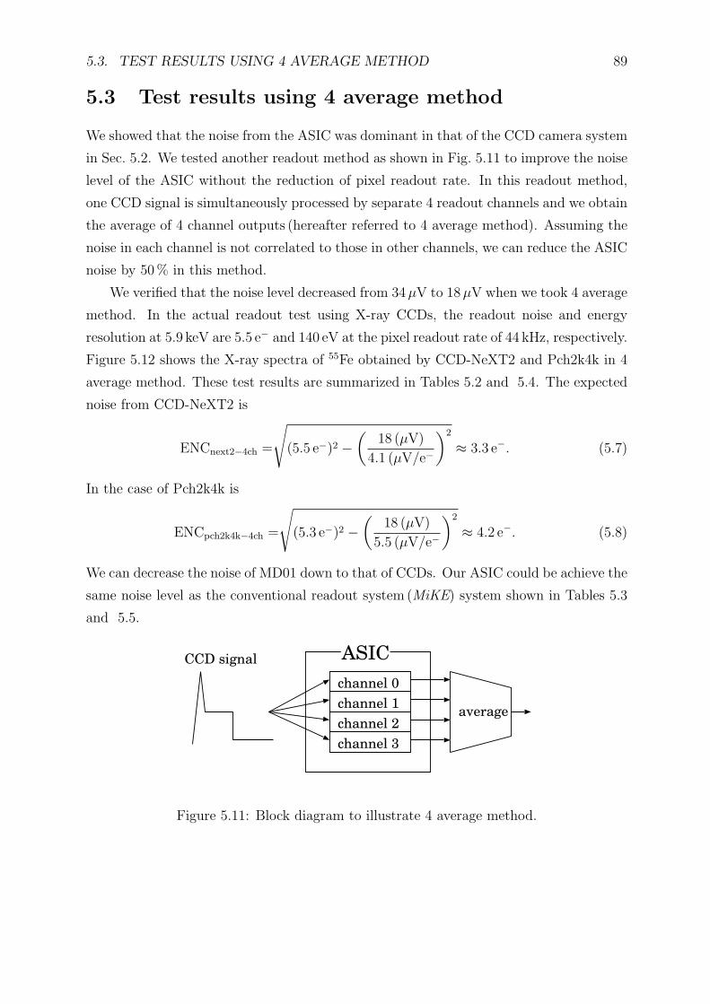
5.3. TEST RESULTS USING 4 AVERAGE METHOD 89
5.3 Test results using 4 average method
We showed that the noise from the ASIC was dominant in that of the CCD camera system
in Sec. 5.2. We tested another readout method as shown in Fig. 5.11 to improve the noise
level of the ASIC without the reduction of pixel readout rate. In this readout method,
one CCD signal is simultaneously processed by separate 4 readout channels and we obtain
the average of 4 channel outputs (hereafter referred to 4 average method). Assuming the
noise in each channel is not correlated to those in other channels, we can reduce the ASIC
noise by 50% in this method.
We verified that the noise level decreased from 34µV to 18µV when we took 4 average
method. In the actual readout test using X-ray CCDs, the readout noise and energy
resolution at 5.9 keV are 5.5 e− and 140 eV at the pixel readout rate of 44 kHz, respectively.
Figure 5.12 shows the X-ray spectra of 55Fe obtained by CCD-NeXT2 and Pch2k4k in 4
average method. These test results are summarized in Tables 5.2 and 5.4. The expected
noise from CCD-NeXT2 is
ENCnext2−4ch =
√(5.5 e−)2 −
(18 (µV)
4.1 (µV/e−
)2
≈ 3.3 e−. (5.7)
In the case of Pch2k4k is
ENCpch2k4k−4ch =
√(5.3 e−)2 −
(18 (µV)
5.5 (µV/e−
)2
≈ 4.2 e−. (5.8)
We can decrease the noise of MD01 down to that of CCDs. Our ASIC could be achieve the
same noise level as the conventional readout system (MiKE) system shown in Tables 5.3
and 5.5.
channel 0
averagechannel 1
channel 2
channel 3
ASICCCD signal
Figure 5.11: Block diagram to illustrate 4 average method.
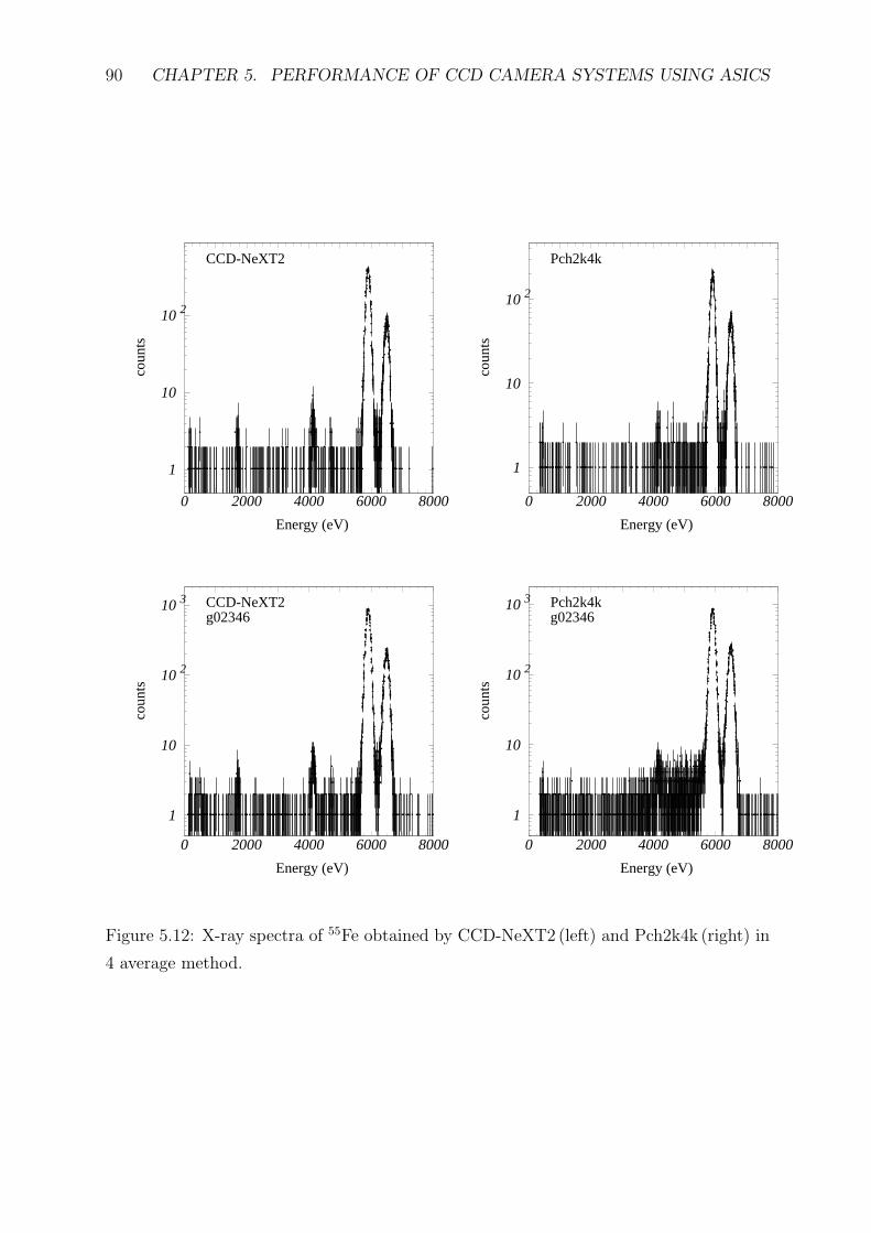
90 CHAPTER 5. PERFORMANCE OF CCD CAMERA SYSTEMS USING ASICS
1
10
10 2
0 2000 4000 6000 8000
coun
ts
Energy (eV)
CCD-NeXT2
1
10
10 2
0 2000 4000 6000 8000co
unts
Energy (eV)
Pch2k4k
1
10
10 2
10 3
0 2000 4000 6000 8000
coun
ts
Energy (eV)
g02346CCD-NeXT2
1
10
10 2
10 3
0 2000 4000 6000 8000
coun
ts
Energy (eV)
Pch2k4kg02346
Figure 5.12: X-ray spectra of 55Fe obtained by CCD-NeXT2 (left) and Pch2k4k (right) in
4 average method.
Chapter 6
High speed drive and readout
system for X-ray CCDs
6.1 C-link system
We evaluated the performance of the ASICs using the X-ray CCDs at the moderate pixel
rate (40 kHz) as shown in Chapter 5. The ASICs properly work at the pixel rate up to
600 kHz as shown in Chapter 4. For the next step, we test the readout of X-ray CCDs
at the high pixel rate of more than 100 kHz. The readout test of CCD using the ASIC
previously had been performed by MiKE system. However, if we operate the ASIC at
the pixel rate of more than 40 kHz by MiKE system, we need to considerably revise its
system. Additionally, the data rate of PC/104 bus, which is utilized in our DP shown in
Fig. 5.2 (left), is less than 8 MByte/sec. Assuming the pixel rate of 600 kHz and the data
size is 2 byte/pixel, the maximum number of channels is up to 6. We should increase the
number of readout nodes of CCDs to speed up the frame rate. We are developing the new
readout system to realize the multi-readout employing ∼10 ASICs at the high pixel rate.
Figure 6.1 shows the block diagram of this new readout system (hereafter referred to C-
link system). C-link system consists of Camera Link, ARM processor, Digital Electronics
InterFace (DE I/F), driver, drain and video boards.
6.1.1 Camera Link board
We employed the commercial framegrabber board (PCI DV C-Link), which supports
Camera Link, provided by Engineering Design Team (EDT), Inc. for data acquisition.
Camera Link is an interface protocol to standardize the interconnects between cameras
and framegrabbers as detained in (Camera Link spec). Since the several camera and
91
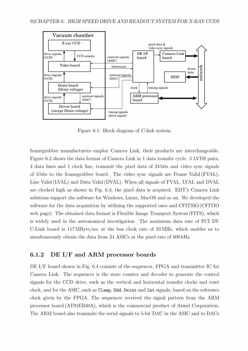
92CHAPTER 6. HIGH SPEED DRIVE AND READOUT SYSTEM FOR X-RAY CCDS
X-ray CCD
Driver board
Drain board(Drain voltage)
Video board
controal signals
(ASIC)
bitstreams
controal signals
(DAC)
timing signals
(drive signal)
drive signals
(CCD)
DE I/Fboard
ARM processorboard
timing signalsclock
Camera Linkboard
HDD
netw
ork
CCD outputs
Vacuum chamber
pixel data &
video sync signals
controal signals
(DAC)drive signals
(CCD)
drive signals
(CCD)
(except Drain voltage)
frame
data
Figure 6.1: Block diagram of C-link system.
framegrabber manufacturers employ Camera Link, their products are interchangeable.
Figure 6.2 shows the data format of Camera Link in 1 data transfer cycle. 5 LVDS pairs,
4 data lines and 1 clock line, transmit the pixel data of 24 bits and video sync signals
of 3 bits to the framegrabber board. The video sync signals are Frame Valid (FVAL),
Line Valid (LVAL) and Data Valid (DVAL). When all signals of FVAL, LVAL and DVAL
are clocked high as shown in Fig. 6.3, the pixel data is acquired. EDT’s Camera Link
solutions support the software for Windows, Linux, MacOS and so on. We developed the
software for the data acquisition by utilizing the supported ones and CFITSIO (CFITIO
web page). The obtained data format is Flexible Image Transport System (FITS), which
is widely used in the astronomical investigation. The maximum data rate of PCI DV
C-Link board is 117MByte/sec at the bus clock rate of 33MHz, which enables us to
simultaneously obtain the data from 24 ASICs at the pixel rate of 600 kHz.
6.1.2 DE I/F and ARM processor boards
DE I/F board shown in Fig. 6.4 consists of the sequencer, FPGA and transmitter IC for
Camera Link. The sequencer is the state counter and decoder to generate the control
signals for the CCD drive, such as the vertical and horizontal transfer clocks and reset
clock, and for the ASIC, such as Clamp, Odd, Deint and Int signals, based on the reference
clock given by the FPGA. The sequencer received the signal pattern from the ARM
processor board (AT91EB40A), which is the commercial product of Atmel Corporation.
The ARM board also transmits the serial signals to 5-bit DAC in the ASIC and to DACs
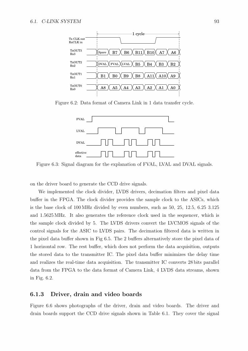
6.1. C-LINK SYSTEM 93
Spare B7 B6 B11 B10 A7 A6
DVAL FVAL LVAL B5 B4 B3 B2
B1 B0 B9 B8 A11 A10 A9
A8 A5 A4 A3 A2 A1 A0
Tx CLK outRxCLK in
TxOUT3Rx3
TxOUT2Rx2
TxOUT1Rx1
TxOUT0Rx0
1 cycle
Figure 6.2: Data format of Camera Link in 1 data transfer cycle.
FVAL
LVAL
DVAL
effective
data
Figure 6.3: Signal diagram for the explanation of FVAL, LVAL and DVAL signals.
on the driver board to generate the CCD drive signals.
We implemented the clock divider, LVDS drivers, decimation filters and pixel data
buffer in the FPGA. The clock divider provides the sample clock to the ASICs, which
is the base clock of 100MHz divided by even numbers, such as 50, 25, 12.5, 6.25 3.125
and 1.5625MHz. It also generates the reference clock used in the sequencer, which is
the sample clock divided by 5. The LVDS drivers convert the LVCMOS signals of the
control signals for the ASIC to LVDS pairs. The decimation filtered data is written in
the pixel data buffer shown in Fig 6.5. The 2 buffers alternatively store the pixel data of
1 horizontal row. The rest buffer, which does not perform the data acquisition, outputs
the stored data to the transmitter IC. The pixel data buffer minimizes the delay time
and realizes the real-time data acquisition. The transmitter IC converts 28 bits parallel
data from the FPGA to the data format of Camera Link, 4 LVDS data streams, shown
in Fig. 6.2.
6.1.3 Driver, drain and video boards
Figure 6.6 shows photographs of the driver, drain and video boards. The driver and
drain boards support the CCD drive signals shown in Table 6.1. They cover the signal
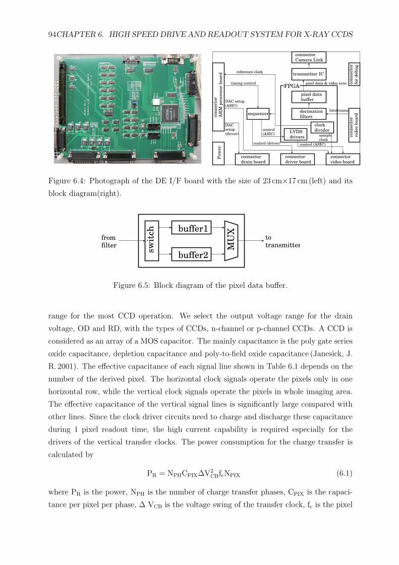
94CHAPTER 6. HIGH SPEED DRIVE AND READOUT SYSTEM FOR X-RAY CCDS
con
nect
or
AR
M p
roce
ssor
board
Pow
er
connectordrain board
connectordriver board
connectorvideo board
con
nect
or
vid
eo b
oard
decimation filters
pixel databuffer
connectorCamera Link
transmitter IC
sequencer
clockdividerLVDS
drivers
FPGA
con
nect
or
for
deb
ug
DAC setup(ASIC)
DACsetup(driver)
reference clock
pixel data & video sync
bitstreams
control (driver)
control(ASIC)
control (ASIC)
sampleclock
timing control
Figure 6.4: Photograph of the DE I/F board with the size of 23 cm×17 cm (left) and its
block diagram(right).
buffer1
buffer2
sw
itch
MU
Xfrom
filter
to
transmitter
Figure 6.5: Block diagram of the pixel data buffer.
range for the most CCD operation. We select the output voltage range for the drain
voltage, OD and RD, with the types of CCDs, n-channel or p-channel CCDs. A CCD is
considered as an array of a MOS capacitor. The mainly capacitance is the poly gate series
oxide capacitance, depletion capacitance and poly-to-field oxide capacitance (Janesick, J.
R. 2001). The effective capacitance of each signal line shown in Table 6.1 depends on the
number of the derived pixel. The horizontal clock signals operate the pixels only in one
horizontal row, while the vertical clock signals operate the pixels in whole imaging area.
The effective capacitance of the vertical signal lines is significantly large compared with
other lines. Since the clock driver circuits need to charge and discharge these capacitance
during 1 pixel readout time, the high current capability is required especially for the
drivers of the vertical transfer clocks. The power consumption for the charge transfer is
calculated by
PR = NPHCPIX∆V2CBfcNPIX (6.1)
where PR is the power, NPH is the number of charge transfer phases, CPIX is the capaci-
tance per pixel per phase, ∆ VCB is the voltage swing of the transfer clock, fc is the pixel
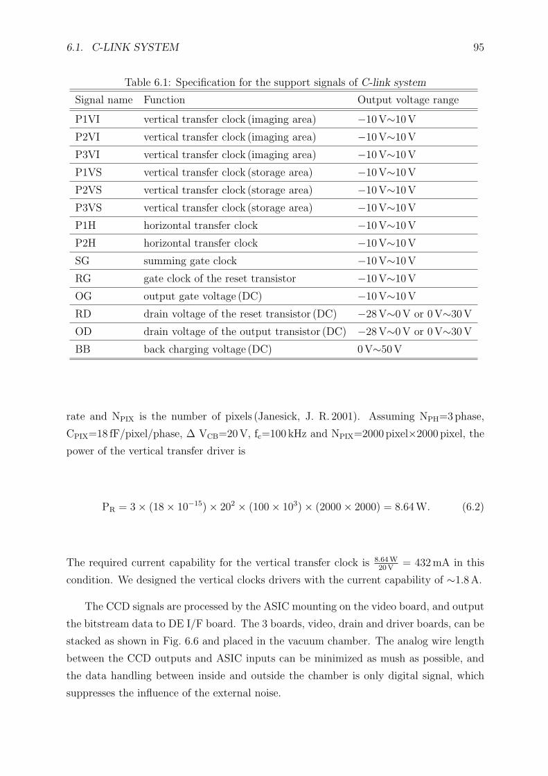
6.1. C-LINK SYSTEM 95
Table 6.1: Specification for the support signals of C-link system
Signal name Function Output voltage range
P1VI vertical transfer clock (imaging area) −10V∼10V
P2VI vertical transfer clock (imaging area) −10V∼10V
P3VI vertical transfer clock (imaging area) −10V∼10V
P1VS vertical transfer clock (storage area) −10V∼10V
P2VS vertical transfer clock (storage area) −10V∼10V
P3VS vertical transfer clock (storage area) −10V∼10V
P1H horizontal transfer clock −10V∼10V
P2H horizontal transfer clock −10V∼10V
SG summing gate clock −10V∼10V
RG gate clock of the reset transistor −10V∼10V
OG output gate voltage (DC) −10V∼10V
RD drain voltage of the reset transistor (DC) −28V∼0V or 0 V∼30V
OD drain voltage of the output transistor (DC) −28V∼0V or 0 V∼30V
BB back charging voltage (DC) 0V∼50V
rate and NPIX is the number of pixels (Janesick, J. R. 2001). Assuming NPH=3phase,
CPIX=18 fF/pixel/phase, ∆ VCB=20V, fc=100 kHz and NPIX=2000 pixel×2000 pixel, the
power of the vertical transfer driver is
PR = 3 × (18 × 10−15) × 202 × (100 × 103) × (2000 × 2000) = 8.64 W. (6.2)
The required current capability for the vertical transfer clock is 8.64W20V
= 432 mA in this
condition. We designed the vertical clocks drivers with the current capability of ∼1.8A.
The CCD signals are processed by the ASIC mounting on the video board, and output
the bitstream data to DE I/F board. The 3 boards, video, drain and driver boards, can be
stacked as shown in Fig. 6.6 and placed in the vacuum chamber. The analog wire length
between the CCD outputs and ASIC inputs can be minimized as mush as possible, and
the data handling between inside and outside the chamber is only digital signal, which
suppresses the influence of the external noise.
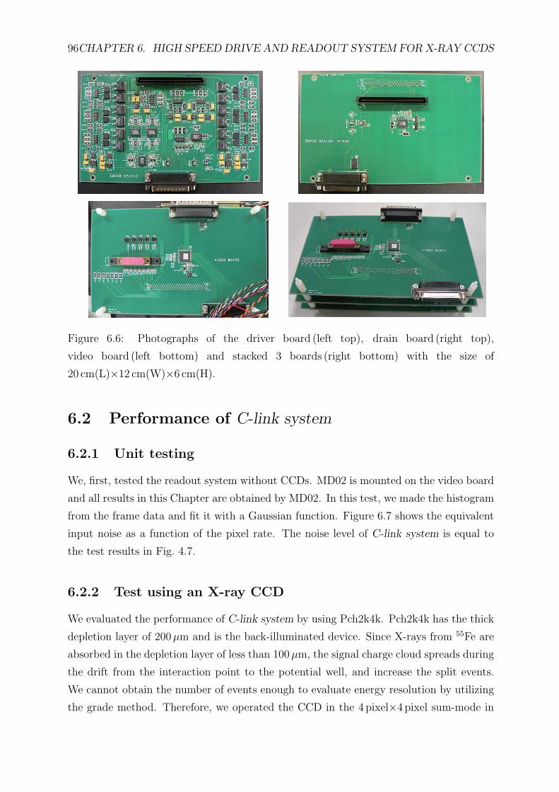
96CHAPTER 6. HIGH SPEED DRIVE AND READOUT SYSTEM FOR X-RAY CCDS
Figure 6.6: Photographs of the driver board (left top), drain board (right top),
video board (left bottom) and stacked 3 boards (right bottom) with the size of
20 cm(L)×12 cm(W)×6 cm(H).
6.2 Performance of C-link system
6.2.1 Unit testing
We, first, tested the readout system without CCDs. MD02 is mounted on the video board
and all results in this Chapter are obtained by MD02. In this test, we made the histogram
from the frame data and fit it with a Gaussian function. Figure 6.7 shows the equivalent
input noise as a function of the pixel rate. The noise level of C-link system is equal to
the test results in Fig. 4.7.
6.2.2 Test using an X-ray CCD
We evaluated the performance of C-link system by using Pch2k4k. Pch2k4k has the thick
depletion layer of 200µm and is the back-illuminated device. Since X-rays from 55Fe are
absorbed in the depletion layer of less than 100µm, the signal charge cloud spreads during
the drift from the interaction point to the potential well, and increase the split events.
We cannot obtain the number of events enough to evaluate energy resolution by utilizing
the grade method. Therefore, we operated the CCD in the 4 pixel×4 pixel sum-mode in
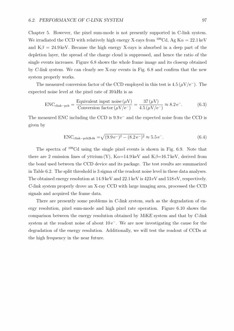
6.2. PERFORMANCE OF C-LINK SYSTEM 97
Chapter 5. However, the pixel sum-mode is not presently supported in C-link system.
We irradiated the CCD with relatively high energy X-rays from 109Cd, Ag Kα = 22.1 keV
and Kβ = 24.9 keV. Because the high energy X-rays is absorbed in a deep part of the
depletion layer, the spread of the charge cloud is suppressed, and hence the ratio of the
single events increases. Figure 6.8 shows the whole frame image and its closeup obtained
by C-link system. We can clearly see X-ray events in Fig. 6.8 and confirm that the new
system properly works.
The measured conversion factor of the CCD employed in this test is 4.5 (µV/e−). The
expected noise level at the pixel rate of 39 kHz is as
ENCclink−pch =Equivalent input noise (µV)
Conversion factor (µV/e−)=
37 (µV)
4.5 (µV/e−)≈ 8.2 e−. (6.3)
The measured ENC including the CCD is 9.9 e− and the expected noise from the CCD is
given by
ENCclink−pch2k4k =√
(9.9 e−)2 − (8.2 e−)2 ≈ 5.5 e−. (6.4)
The spectra of 109Cd using the single pixel events is shown in Fig. 6.9. Note that
there are 2 emission lines of yttrium (Y), Kα=14.9 keV and Kβ=16.7 keV, derived from
the bond used between the CCD device and its package. The test results are summarized
in Table 6.2. The split threshold is 3 sigma of the readout noise level in these data analyses.
The obtained energy resolution at 14.9 keV and 22.1 keV is 423 eV and 518 eV, respectively.
C-link system properly drove an X-ray CCD with large imaging area, processed the CCD
signals and acquired the frame data.
There are presently some problems in C-link system, such as the degradation of en-
ergy resolution, pixel sum-mode and high pixel rate operation. Figure 6.10 shows the
comparison between the energy resolution obtained by MiKE system and that by C-link
system at the readout noise of about 10 e−. We are now investigating the cause for the
degradation of the energy resolution. Additionally, we will test the readout of CCDs at
the high frequency in the near future.
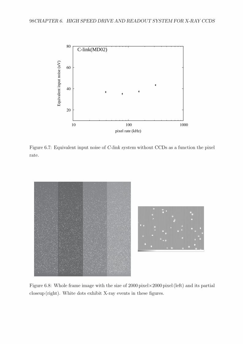
98CHAPTER 6. HIGH SPEED DRIVE AND READOUT SYSTEM FOR X-RAY CCDS
20
40
60
80
10 100 1000
Equ
ival
ent i
nput
noi
se (
uV)
pixel rate (kHz)
C-link(MD02)
Figure 6.7: Equivalent input noise of C-link system without CCDs as a function the pixel
rate.
Figure 6.8: Whole frame image with the size of 2000 pixel×2000 pixel (left) and its partial
closeup (right). White dots exhibit X-ray events in these figures.
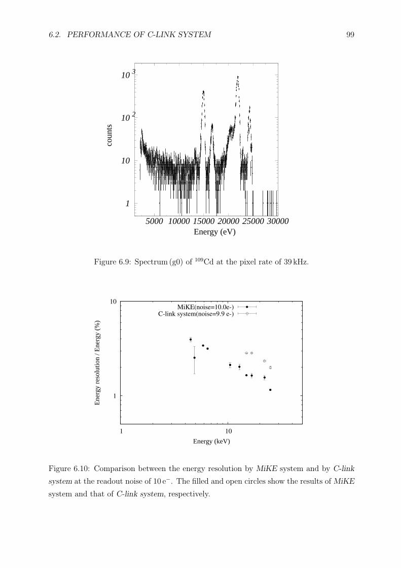
6.2. PERFORMANCE OF C-LINK SYSTEM 99
1
10
10 2
10 3
5000 10000 15000 20000 25000 30000
coun
ts
Energy (eV)
Figure 6.9: Spectrum (g0) of 109Cd at the pixel rate of 39 kHz.
1
10
1 10
Ene
rgy
reso
lutio
n / E
nerg
y (%
)
Energy (keV)
MiKE(noise=10.0e-)C-link system(noise=9.9 e-)
Figure 6.10: Comparison between the energy resolution by MiKE system and by C-link
system at the readout noise of 10 e−. The filled and open circles show the results of MiKE
system and that of C-link system, respectively.
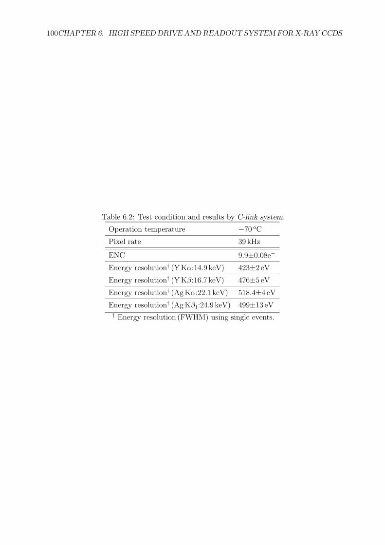
100CHAPTER 6. HIGH SPEED DRIVE AND READOUT SYSTEM FOR X-RAY CCDS
Table 6.2: Test condition and results by C-link system.
Operation temperature −70 oC
Pixel rate 39 kHz
ENC 9.9±0.08e−
Energy resolution† (YKα:14.9 keV) 423±2 eV
Energy resolution† (YKβ:16.7 keV) 476±5 eV
Energy resolution† (AgKα:22.1 keV) 518.4±4 eV
Energy resolution† (AgKβ1:24.9 keV) 499±13 eV† Energy resolution (FWHM) using single events.
Chapter 7
Summary
The combination of an X-ray telescope and an X-ray CCD is the powerful tool for the
observation in X-ray region, which is employed onboard the present X-ray astronomical
satellites and produces excellent results. The X-ray CCDs significantly contribute to the
progress of X-ray astronomy and will remain the standard detector for future missions.
The fabrication technology of the semiconductor is remarkably progressing in these
years. We can develop the full-custom ASIC for the readout of X-ray CCDs by using the
mixed-signal CMOS technology. The ASIC practically enables us to increase the number
of the readout channels for high frame rate, and easily construct a CCD camera system
under limitations of volume and power consumption onboard satellites. We fabricated
ASICs with the size of 3 mm × 3mm by the TSMC 0.35µm CMOS process. There are 4
readout channels in 1 chip. One channel is composed of a preamplifier, 5-bit DAC and ∆Σ
ADC. We developed the new readout method for X-ray CCDs employing the ∆Σ ADC
in our ASICs. This ADC functions not only as the ADC but also as the band-pass filter,
which makes the circuit configuration relatively simple compared with the conventional
systems. So far, we have fabricated 4 types of ASICs : MD01, MND01, MD02 and MND02.
Their performances and problems are summarized in the following itemization.
1. MD01 : The noise level is 42µV and the power consumption is 79mW at the pixel
rate of 156 kHz. The input range is 40mV and the INL is 0.2%. The maximum
pixel rate is 156 kHz. The problems are the malfunction of the LVDS drivers and
the low pixel rate, which is derived from the transistor without the NLDD region
in the digital circuits.
2. MND01 : The noise level is 48µV and the power consumption is 89mW at the pixel
rate of 156 kHz. The input range is 20 mV∼200mV and the INL is 1.2%. The
maximum pixel rate is improved to be 625 kHz. The problems are the decrease of
101
102 CHAPTER 7. SUMMARY
the input range and the degradation of the noise level and the INL, which is derived
from the ESD layer.
3. MD02 : The noise level is 41µV and the power consumption per chip is 92mW at
the pixel rate of 156 kHz. The input range is 40 mV and the INL is 0.2 %. The
maximum pixel rate is 625 kHz. We can confirm that all the fundamental problems
have been solved.
4. MND02 : We implemented the low noise operational amplifier in MND02. The noise
level is 29µV and the power consumption per chip is 168mW at the pixel rate of
156 kHz. The input range is 40mV∼400mV and the INL is 0.2%. The maximum
pixel rate is 625 kHz.
We are developing the SXI, X-ray CCD camera system for ASTRO-H. 2 types of
X-ray CCDs for the SXI prototype models, called CCD-NeXT2 and Pch2k4k, presently
have been developed. We evaluated the performance of the camera system using the
ASIC (MD01) and these CCD devices. The readout noise and energy resolution (FWHM)
at 5.9 keV were 7.5 e− and 150 eV (g0) at the pixel rate of 40 kHz when using Pch2k4k.
Since the noise from the ASIC was dominant in the total readout noise, we simultaneously
processed one CCD signal by separate 4 channels and obtained their average to reduce
the noise component from the ASIC by half. This fact indicates that four channels
in one chip are completely independent of each other, indicating the proper design of
the analog circuit. In this readout method, we achieved the readout noise and energy
resolution (FWHM) at 5.9 keV were 5.3 e− and 140 eV (g0) at the pixel rate of 40 kHz,
respectively. We are now preparing the test setup for MND02 and expect to achieve the
readout noise of a few electrons.
ASTRO-H will be launched into the low earth orbit of 550 km. The devices onboard
the satellite will be mainly damaged by protons during the passage of the SAA. Therefore,
we tested the TID effect of the ASIC (MD01) by using a 200MeV proton beam at HIMAC.
The indication of the radiation damage did not appear at the TID of up to 17 krad.
Additionally, all function was recovered after the annealing at the room temperature.
Through the test results, we can verify that the ASIC (MD01) surrounded by Al with the
thickness of 1mm meets the radiation tolerance in space required for ASTRO-H.
We are developing the new X-ray CCD camera system (C-link system) utilizing the
ASIC and the Camera Link to realize the multi-readout of CCD signals at the high pixel
rate. We obtained the proper frame image and spectrum at the pixel rate of 40 kHz.
The readout noise and energy resolution (FWHM) at 22.1 keV are 9.9 e− and 518 eV (g0),
respectively. We will test the readout of the CCD by C-link system at the high frequency

103
of more than 100 kHz in near future. We expect that the C-link system enables anyone
to easily construct the compact readout system for X-ray CCDs with low noise and high
pixel rate.

Acknowledgments
First of all, I sincerely thank to Prof. H.Tsunemi for giving me an excellent subject
of research, an development of ASICs, and his continuous guidance. I thank to Prof.
K.Hayashida and Dr. K.Torii for their useful advice in meetings and supports at the
ground calibration of the XIS. I could see and test the FM model of the XIS, which is
a valuable experience in my graduate period. I am grateful to Dr. E.Miyata for her
technical supports of X-ray CCD experiments. These experiences were very useful in the
development of ASCIs. Dr. N.Anabuki supported me with the designs of VHDL and
software in experiments. Dr. H.Nakajima helped me through the ASIC developments
and checked my papers. Dr. H.Ozawa commented on my test results and gave me
improvement plans. Dr. M.Namiki held a seminar for data analyses of X-ray astronomy.
This was a valuable opportunity for me. They often took me out for drink, which made
me feel relaxed. I wish to thank all of members in X-ray Astronomy Group in Osaka
University.
I would like to thank to N.Kitamura, T.Mitani and T.Takashima for their techni-
cal supports at the radiation test of the ASIC in HIMAC/NIRS. The source data of
figures 4.19 and 4.20 are by courtesy of JAXA Space Environment Group.
I especially thank to collaborators of Drs. J.P.Doty and H.Ikeda. Dr. J.P.Doty is a
worldwide specialist for X-ray CCD camera systems. It is a great experience that I could
develop the ASICs with him. Dr. H.Ikeda taught me a basics of CMOS circuits and a
SPICE simulation, and also advised me as to what I should do in the experiments and data
analyses through the graduate period. Additionally, OPEN IP that is implemented in our
ASICs is designed by him. My research can’t be successful without their collaboration.
This study was also carried out as part of the 21st Century COE Program, ‘Towards
a new basic science: depth and synthesis’. I am supported by JSPS Research Fellowship
for Young Scientists.
I would like to show my deepest appreciation for my family. Finally, I hope for a great
success of ASTRO-H especially for the SXI.
February 2, 2009 Daiuske Matsuura
105

106 ACKNOWLEDGMENTS
References
ASCA web page, http://heasarc.gsfc.nasa.gov/docs/asca/
Bookbinder, J. et al. 2008, Proc. SPIE, 7011, 2B
Camera Link spec, http://www.qmt.ch/ library/cameralink specifications 1.1.pdf
CFITIO web page, http://heasarc.nasa.gov/lheasoft/fitsio/fitsio.html
comedi web page, http://www.comedi.org/
Cyber Shuttle web page, http://www.toptdc.com/tsmc/index.html
Digian web page, http://www.digian.co.jp/
Doty, J. P. 2006a, US patent application serial number 11/307435, international patent
application serial number PCT/US2006/004330
Doty, J.P. et al. 2006b, Proc. SPIE, 6276, 62761P
gEDE web page, http://www.geda.seul.org/
Garmire, G.P. et al. 2003, Proc. SPIE, 4851, 28
Herrmann, S. et al. 2007, NSS ’07, IEEE, 3, 2398
Hiraga, J. 2002, PHD thesis, Osaka University
Inose, H. et al. 1962 IRE Trans. on Space Electronics and Telemetry, 8, 204
Janesick, J. R. 2001, SPIE PRESS
Karcher, A. et al. 2007, NSS ’07, IEEE, 2, 1069
Koyama, K. et al. 2007a, PASJ, 59, 23
LSE64 web page, http://www.noqsi.com/images/lse64-0.3.zip
107
108 REFERENCES
Matsuura, D. et al. 2006a, Proc. SPIE, 6276, 627612
Matsuura, D. et al. 2006b, JJAP, 45, 8904
Matsuura, D. et al. 2007, Nucl. Instr. and Meth. A, A570, 140
Matsushita, T. et al. 1995, Nucl. Instr. and Meth. A,336, 336
Mitsuda, K. et al. 2007, PASJ, 59, 1
Miyata, E. et al. 2006, Nucl. Instr. and Meth. A, 568, 149
Miyata, E. et al. 2001, Nucl. Instr. and Meth. A, 459, 157
Nakaya, H. et al. 2008, Proc. SPIE, 7014, 70144X
MOSIS web page, http://www.mosis.com/
Nakajima, H. et al. 2008, IEEE Press, now submitted
Open IP web page, http://research.kek.jp/people/ikeda/openIP/
Parmar, A. et al. 2006, Proc. SPIE, 6266, 50P
Rainey, P.M. 1921, U.S. Patent 1, 608, 527
Richard, S. et al. 2005, IEEE Press
Struder, L. et al. 2001, A&A, 365, 18
SUN-S web page, http://www.sun-s.jp/
Takahashi, T. et al. 2008, Proc. SPIE, 7011, 70110O
Tanaka, Y. et al. 1994, PASJ, 46, 37
TSMC web page, http://www.mosis.com/products/fab/vendors/tsmc/tsmc035/
Tsunemi, H. et al. 2007, Nucl. Instr. and Meth. A, 579, 866
Tsunemi, H. et al. 2008, Proc. SPIE, 7011, 70110Q
Turner, M.L.J. et al. 2001, A&A, 365, 27
Yamashita, A. et al. 1997, IEEE Trans. Nucl. Sci, 44, 847
Yamashita, A et al. 1999 Nucl. Instr. and Meth. A, 436, 68
Yokoyama, M. et al. 2001, IEEE Trans. Nucl. Sci., 48, 440