Embed Size (px)
Citation preview
DESIGN OF READ/WRITE CIRCUITS SUITABLEFOR MEMRISTOR-BASED MEMORY ARRAYS
By
Mohamed Sayed Ahmed Mohamed Elshamy
A Thesis Submitted to theFaculty of Engineering at Cairo University
in Partial Fulfillment of theRequirements for the Degree of
MASTER OF SCIENCEin
Electronics and Communications
FACULTY OF ENGINEERING, CAIRO UNIVERSITYGIZA, EGYPT
2014
DESIGN OF READ/WRITE CIRCUITS SUITABLEFOR MEMRISTOR-BASED MEMORY ARRAYS
By
Mohamed Sayed Ahmed Mohamed Elshamy
A Thesis Submitted to theFaculty of Engineering at Cairo University
in Partial Fulfillment of theRequirements for the Degree of
MASTER OF SCIENCEin
Electronics and Communications
Under the Supervision of
Prof. Dr. Mohamed Sameh Saied Dr. Hassan Moustafa HassanProfessor of Electronics Doctor of Electronics
Electronics and Communications Department Electronics and Communications Department
Faculty of Engineering, Cairo University Faculty of Engineering, Cairo University
FACULTY OF ENGINEERING, CAIRO UNIVERSITYGIZA, EGYPT
2014
DESIGN OF READ/WRITE CIRCUITS SUITABLEFOR MEMRISTOR-BASED MEMORY ARRAYS
By
Mohamed Sayed Ahmed Mohamed Elshamy
A Thesis Submitted to theFaculty of Engineering at Cairo University
in Partial Fulfillment of theRequirements for the Degree of
MASTER OF SCIENCEin
Electronics and Communications
Approved by the Examining Committee:
Prof. Dr. Mohamed Sameh Saied, Thesis Main Advisor
Prof. Dr. Mohamed Fathi, Internal Examiner
Prof. Dr. Hassanein Amer Hamed, External Examiner
Professor of Electronics at Electronics and Communications DepartmentFaculty of Engineering, American University in Cairo (AUC)
FACULTY OF ENGINEERING, CAIRO UNIVERSITYGIZA, EGYPT
2014

Engineer’s Name: Mohamed Sayed Ahmed Mohamed ElshamyDate of Birth: 21/3/1986Nationality: EgyptianE-mail: eng [email protected]: +2 0122 2589213Address: 12, Alabour st., from Elbalsem, MateryaRegistration Date: 10/10/2010Awarding Date: ......./......./...........Degree: Master of ScienceDepartment: Electronics and Communications
Supervisors:Prof. Dr. Mohamed Sameh SaiedDr. Hassan Moustafa Hassan
Examiners:Prof. Dr. Hassanein Amer Hamed (External examiner)Prof. Dr. Mohamed Fathi (Internal examiner)Prof. Dr. Mohamed Sameh Saied (Thesis main advisor)
Title of Thesis:DESIGN OF READ/WRITE CIRCUITS SUITABLE FOR MEMRISTOR-BASED MEMORY ARRAYS
Key Words:Memristor; Read/write; Memory; nonvolatile; Memory arrays
Summary:Memristor, which known as the missing fourth circuit element, is a potentialcandidate for the next-generation memory. Memristor has received extraattention in the last few years. In this thesis presents three novel Read/Writecircuits suitable for Memristor-based memory arrays. The advantages ofthe proposed Read/Write circuits are threefold. Firstly, two of the proposedcircuits have non-destructive successive reading cycle capability. Secondly,it occupies less die area. Finally, the proposed Read/Write circuits have lesspower consumption and delay time compared to other Read/Write circuits.

Acknowledgments
I am truly surprised when I think of how much I have learned and all of therich experiences I have been blessed with over the course of my Master degree.For this, I am grateful to all those who not only helped me in my pursuit ofmy MSc degree, but have made the past few years so very memorable.
I first must thank Allah for, among many other things, allowing me to come tothis point of my life and for giving me the strength to overcome the adversitiesI have faced along the way. I would like to thank my supervisors, ProfessorMohamed Sameh Said and Doctor Hassan Moustafa, for their guidance andsupport over the past few years. They were supportive of very ambitiousresearch targets, and I am grateful that they gave me the freedom to explorea very interesting research area. I would also like to thank the members ofmy thesis committee for taking time to review my thesis and for their veryhelpful comments and suggestions. I would like to extend my gratitude to theASRT awards department members for their help and supporting fund.
Last, but not least, I thank my family, who have been my support and thesource of my motivation from elementary school and all the way through gradschool. I will never be able to repay the tremendous sacrifices they have madefor me, but I hope that they may in some way feel rewarded in any of thepursuits in which I am successful in. This thesis is dedicated to them.
i

Dedication
“To my parents, whose unbounded sacrifices have brought me this far.”
Mohamed Elshamy
ii
Table of Contents
Acknowledgments i
Dedication ii
Table of Contents iii
List of Tables v
List of Figures vi
Nomenclature ix
Abstract x
1 Introduction 11.1 Motivation . . . . . . . . . . . . . . . . . . . . . . . . . . . . . . . . . . 11.2 Memory Effects in Memristor . . . . . . . . . . . . . . . . . . . . . . . 41.3 Thesis Objectives . . . . . . . . . . . . . . . . . . . . . . . . . . . . . . 51.4 Thesis Outline . . . . . . . . . . . . . . . . . . . . . . . . . . . . . . . . 5
2 Background 72.1 Emerging Non-Volatile Memory Technology . . . . . . . . . . . . . . . 7
2.1.1 Phase-Change RAM (PCRAM) . . . . . . . . . . . . . . . . . . 82.1.2 Magnetoresistive RAM (MRAM) . . . . . . . . . . . . . . . . . 102.1.3 Ferroelectric RAM (FRAM) . . . . . . . . . . . . . . . . . . . . 112.1.4 Resistive RAM (RRAM) . . . . . . . . . . . . . . . . . . . . . . 11
2.2 Memristors . . . . . . . . . . . . . . . . . . . . . . . . . . . . . . . . . 12
3 Memristive Systems 173.1 Polymeric Memristor . . . . . . . . . . . . . . . . . . . . . . . . . . . . 173.2 Metal-insulator Phase Transition Memristive Systems . . . . . . . . . . . 183.3 Resistance Switching Memristors . . . . . . . . . . . . . . . . . . . . . . 193.4 Spintronic Memristors . . . . . . . . . . . . . . . . . . . . . . . . . . . 213.5 Comparison between TiO2 Memristor and Spintronic Memristor . . . . . 22
3.5.1 Working Principle . . . . . . . . . . . . . . . . . . . . . . . . . 223.5.2 Device Properties . . . . . . . . . . . . . . . . . . . . . . . . . . 243.5.3 Summery of the Comparison . . . . . . . . . . . . . . . . . . . . 29
4 Memristor Models and Applications 314.1 Memristor Models . . . . . . . . . . . . . . . . . . . . . . . . . . . . . 31
4.1.1 Mathematical Models . . . . . . . . . . . . . . . . . . . . . . . . 314.1.2 Spice Models . . . . . . . . . . . . . . . . . . . . . . . . . . . . 324.1.3 Verilog-A Models . . . . . . . . . . . . . . . . . . . . . . . . . . 33
4.2 Memristor Applications . . . . . . . . . . . . . . . . . . . . . . . . . . . 34
iii
5 Memory design insights and new proposed circuits 435.1 Memristor-based Memory Design Insights . . . . . . . . . . . . . . . . . 43
5.1.1 Design Considerations . . . . . . . . . . . . . . . . . . . . . . . 435.1.2 Memristor in Memory Arrays . . . . . . . . . . . . . . . . . . . 45
5.2 New Proposed Circuits . . . . . . . . . . . . . . . . . . . . . . . . . . . 475.2.1 First Proposed Circuit . . . . . . . . . . . . . . . . . . . . . . . 47
5.2.1.1 Writing Operation . . . . . . . . . . . . . . . . . . . . 475.2.1.2 Reading Operation . . . . . . . . . . . . . . . . . . . . 495.2.1.3 Simulation Results . . . . . . . . . . . . . . . . . . . . 49
5.2.2 Second Proposed Circuit . . . . . . . . . . . . . . . . . . . . . . 545.2.2.1 Writing Operation . . . . . . . . . . . . . . . . . . . . 555.2.2.2 Reading Operation . . . . . . . . . . . . . . . . . . . . 555.2.2.3 Simulation Results . . . . . . . . . . . . . . . . . . . . 57
5.2.3 Third Proposed Circuit . . . . . . . . . . . . . . . . . . . . . . . 595.2.3.1 Writing Operation . . . . . . . . . . . . . . . . . . . . 605.2.3.2 Reading Operation . . . . . . . . . . . . . . . . . . . . 605.2.3.3 Implementation of SW3 . . . . . . . . . . . . . . . . . 615.2.3.4 Simulation Results . . . . . . . . . . . . . . . . . . . . 61
5.3 Comparison of the proposed circuits with Previously Published Read/WriteCircuits . . . . . . . . . . . . . . . . . . . . . . . . . . . . . . . . . . . 63
6 Discussion and Conclusions 736.1 Contributions . . . . . . . . . . . . . . . . . . . . . . . . . . . . . . . . 736.2 Published/Submitted papers . . . . . . . . . . . . . . . . . . . . . . . . . 736.3 Future Work . . . . . . . . . . . . . . . . . . . . . . . . . . . . . . . . . 74
References 75
Appendix A Memristor verilog-A model [97] 85
Appendix B Adding Verilog-A to Cadence Spectre simulation tools 93
iv
List of Tables
2.1 Brief comparison between emerging non-volatile memories. . . . . . . . 12
3.1 Comparison between TiO2 thin film and spintronic memristor. . . . . . . 29
4.1 Summery of the comparison between the three models discussed in [93]. . 324.2 Summary of the comparison between the three spice models submitted in
[94-96]. . . . . . . . . . . . . . . . . . . . . . . . . . . . . . . . . . . . 334.3 Summary of the comparison between different memristive device models
submitted in [98]. . . . . . . . . . . . . . . . . . . . . . . . . . . . . . . 33
5.1 Memristor TEAM model main parameters values [98] . . . . . . . . . . . 505.2 Comparison between the reviewed solutions for the sneak paths problem
in the first proposed circuit. . . . . . . . . . . . . . . . . . . . . . . . . . 545.3 Comparison between the reviewed solutions for the sneak paths problem
in the second proposed circuit. . . . . . . . . . . . . . . . . . . . . . . . 595.4 Comparison between the reviewed solutions for the sneak paths problem
in the third proposed circuit. . . . . . . . . . . . . . . . . . . . . . . . . 635.5 Comparison between the proposed circuit in this article and the circuit
introduced in [13]. . . . . . . . . . . . . . . . . . . . . . . . . . . . . . 70
v
List of Figures
1.1 Four fundamental circuit elements: R, C, L, and M (which is the missingfourth element that Chua argued for [1]). . . . . . . . . . . . . . . . . . . 1
1.2 Frequency response of Pinched hysteresis loop in memristive systems [3]. 21.3 (a) Memristor device structure, (b) Equivalent circuit model, and (c)
Memristor symbol [11]. . . . . . . . . . . . . . . . . . . . . . . . . . . . 2
2.1 Plot of CMOS transistor counts against dates of introduction. Note thelogarithmic vertical scale; the line corresponds to exponential growth withtransistor count doubling every two years [50]. . . . . . . . . . . . . . . . 8
2.2 More Moore and more than Moore [52]. . . . . . . . . . . . . . . . . . . 92.3 A cross sectional area of a Phase-Change Random Access Memory [53]. . 92.4 An MTJ device where (a) shows the device low resistance state as the
magnetic direction in the two ferromagnetic material is parallel and (b)shows the device high resistance state as the magnetic direction in the twoferromagnetic material is anti-parallel. . . . . . . . . . . . . . . . . . . . 10
2.5 A cross sectional area of FRAM device. . . . . . . . . . . . . . . . . . . 112.6 The proposed symbol for memristor and its basic realization. (a) the ϕ-q
curve, (b) memristor basic realization where an M-R mutator terminated bynonlinear resistor R is used to emulate the device operation, (c) memristorsymbol [1]. . . . . . . . . . . . . . . . . . . . . . . . . . . . . . . . . . 13
2.7 Double valued lissajous figure with symmetry around the origin (hysteresisloop) [5]. . . . . . . . . . . . . . . . . . . . . . . . . . . . . . . . . . . 16
3.1 Schematic showing four thin-film layer which represents the device struc-ture of polymeric memristor [77]. . . . . . . . . . . . . . . . . . . . . . 17
3.2 Schematic showing four thin-film layers which represents the devicestructure of polymeric memristor [77]. . . . . . . . . . . . . . . . . . . . 18
3.3 Schematic showing a phase transition driven memristive device [82]. . . . 193.4 Hysteresis I-V curves under which three ramped voltage pulses are applied
[82]. . . . . . . . . . . . . . . . . . . . . . . . . . . . . . . . . . . . . . 193.5 Memristor structure and symbol. (a) memristor architecture and the cir-
cuit corresponding symbol. (b) memristor crossbar architecture showingmemristor location between two perpendicular nano-wires. . . . . . . . . 20
3.6 Applying symmetrical alternating-current voltage bias results in the I-Vhysteresis loop [10]. . . . . . . . . . . . . . . . . . . . . . . . . . . . . . 21
3.7 Spintronic memristor based on magnetic-domain-wall motion and theequivalent circuit. . . . . . . . . . . . . . . . . . . . . . . . . . . . . . . 22
3.8 I-V curve of the spintronic memristor with sinusoidal voltage excitation[17]. . . . . . . . . . . . . . . . . . . . . . . . . . . . . . . . . . . . . . 22
3.9 Voltage effect on TiO2 memristor a) when applying positive voltage b)and when applying negative voltage [2]. . . . . . . . . . . . . . . . . . . 23
vi
3.10 Voltage effect on spintronic memristor when the passing current (a) caus-ing the magnetization direction in the free layer to be parallel to themagnetization direction in the reference layer (b) and when causing themagnetization direction in the free layer to be anti-parallel to the magneti-zation direction in the reference layer. . . . . . . . . . . . . . . . . . . . 24
3.11 Applying symmetrical alternating-current voltage bias results in double-loop I-V hysteresis that collapses to a straight line for high frequencies[9]. . . . . . . . . . . . . . . . . . . . . . . . . . . . . . . . . . . . . . . 27
3.12 Calculations of switching time and energy using constant-current magni-tude switching times for ON and OFF switching events. The ON and OFFstates are chosen as won=1.2 nm and wo f f =1.8 nm to reflect a resistanceswitching ratio of 500. These results demonstrate the asymmetry betweenthe ON and OFF switching behavior and show that the switching energydecreases exponentially with the applied current [87]. . . . . . . . . . . . 28
4.1 Memristor read and write circuit that incorporates the circuits discussedin the previous sections [102]. . . . . . . . . . . . . . . . . . . . . . . . 35
4.2 UWB recevier circuit diagram submitted in [68]. . . . . . . . . . . . . . 374.3 Circuit schematic of programmable gain amplifier using memristor, where
RL is the equivalent resistance of the pulse-programmed memristance [103]. 374.4 Low-level structure of the generic CMOL circuit: (a) schematic side view;
(b) the idea of addressing a particular nanodevice, and (c) zoom-in onseveral adjacent pins to show that any nanodevice may be addressed viathe appropriate pin pair [105]. . . . . . . . . . . . . . . . . . . . . . . . 38
4.5 mrFPGA architecture: The programmable routing structure is built upwith metal wires and memristor which are fabricated on top of logic blocksin the same die according to existing memristor fabrication structures [109]. 39
4.6 Circuit architecture of the Memristor-based memory cell. Read/Write(R/W) enable switch is connected to ground for writing process and isswitched to Vx for the reading process. The comparator in the senseamplifier stage compares Vx with the reference voltage Vre f = 0.5×Vin. IfVx >Vre f , the output voltage Vo = VH which represents logic ’1’. Similarly,Vo = VL if Vx < Vre f [13]. . . . . . . . . . . . . . . . . . . . . . . . . . . 40
4.7 Top level block diagram of the circuit proposed in [110]. . . . . . . . . . 41
5.1 Memory crossbar array where the unused memristor terminals are floating. 455.2 Crossbar memory array architecture in (a) unfolded architecture and (b)
1D1M architecture. . . . . . . . . . . . . . . . . . . . . . . . . . . . . . 465.3 Three terminal memristor geometry (a) planar geometry (b) stacked ge-
ometry [117]. . . . . . . . . . . . . . . . . . . . . . . . . . . . . . . . . 475.4 Proposed Read/Write circuit for a Memristor-based memory where, (a)
the proposed circuit (b) writing data circuitry (c) reading data circuitry. . . 485.5 Applying positive voltage to write logic ’1’ (left) and applying a negative
voltage to write logic ’0’ (right). . . . . . . . . . . . . . . . . . . . . . . 495.6 The effect of the applied voltage on the output voltage and the memory
cell state. Left side displays reading logic ’1’ operation whereas the rightside shows reading logic ’0’ operation. . . . . . . . . . . . . . . . . . . . 50
vii
5.7 Writing operation for worst case change in the initial state of the memorydevice for writing (a) logic ’1’ and (b) logic ’0’. Also shown the effect ofthe applied bias voltage (Vin) on the output voltage and the internal stateof memristors M1 and M2. . . . . . . . . . . . . . . . . . . . . . . . . . 52
5.8 Testing the device internal state in case of (a) logic zero, or (b) logic oneis stored. . . . . . . . . . . . . . . . . . . . . . . . . . . . . . . . . . . . 53
5.9 Proposed non-destructive Read/Write circuit for a memristor-based mem-ory. . . . . . . . . . . . . . . . . . . . . . . . . . . . . . . . . . . . . . 55
5.10 The proposed non-destructive Read/Write circuit during the reading oper-ation. . . . . . . . . . . . . . . . . . . . . . . . . . . . . . . . . . . . . 55
5.11 Writing operation simulation results for writing (a) logic ’1’ and (b) logic’0’. . . . . . . . . . . . . . . . . . . . . . . . . . . . . . . . . . . . . . 57
5.12 Reading the internal state of the memory cell for the case of (a) logic ’1’and (b) logic ’0’. . . . . . . . . . . . . . . . . . . . . . . . . . . . . . . 58
5.13 A modified version of the proposed non-destructive Read/Write circuit. . 605.14 The proposed Read/Write circuit during the reading operation, when S W3
is connected to terminal S or terminal S and S W2 is connected to Vr.Applying the positive voltage Vread results in a similar positive voltageat terminal S and a negative voltage at terminal S . Depending on S W3position, Vr will be positive or negative, which makes the diode ON orOFF and Vo to vary from VL to VH . . . . . . . . . . . . . . . . . . . . . . 60
5.15 Reading the internal state of the memory cell for the case of (a) logic ’1’and (b) logic ’0’. Also shown the effect of the applied Read voltage (Vread)on the output levels and the internal state of memristors M1 and M2. . . . 62
5.16 Write signals (bottom) and corresponding memristor states (top) [13]. . . 645.17 Graphical illustration for the reading scheme in [13]. (top) Read pattern,
memristor state, and output voltage when the memristor is storing logic’0’. (bottom) Read pattern, memristor state, and output voltage when thememristor is storing logic ’1’ [13]. . . . . . . . . . . . . . . . . . . . . . 65
5.18 Reading cycle for the circuit in [13] when reading (a) logic ’0’ and (b)logic ’1’. . . . . . . . . . . . . . . . . . . . . . . . . . . . . . . . . . . . 66
5.19 10 successive reading cycles are adopted for the circuit in [13] whenreading (a) logic ’0’ and (b) logic ’1’. It is clear that the circuit in [13]internal state is disturbed and the stored logic value is destroyed. . . . . . 67
5.20 50 successive reading cycles are adopted for the proposed circuit whenreading (a) logic ’0’ and (b) logic ’1’. It is clear that the proposed circuitmaintains the internal state of the memory cell and the stored logic valueis kept as is. . . . . . . . . . . . . . . . . . . . . . . . . . . . . . . . . . 68
5.21 Reading stored data at worst case a) reading logic ’0’ for wn = 0.4 and b)reading logic ’1’ for wn = 0.6. . . . . . . . . . . . . . . . . . . . . . . . 69
B.1 Create new library. . . . . . . . . . . . . . . . . . . . . . . . . . . . . . 93B.2 Naming the new library. . . . . . . . . . . . . . . . . . . . . . . . . . . . 94B.3 Create new file to add the code. . . . . . . . . . . . . . . . . . . . . . . . 94B.4 Appropriate choices for creating the new file. . . . . . . . . . . . . . . . 95B.5 Copy and paste the verilog-A code to the new file. . . . . . . . . . . . . . 95B.6 Draw a symbol for the verilog-A code. . . . . . . . . . . . . . . . . . . . 95
viii

Nomenclature
1D1M one Diode one Memristor1T1C one Transistor one Capacitor1T1M one Transistor one Memristor1T1MTJ one Transistor one Magnetic Tunneling JunctionASIC Application Specific Integrated CircuitCBRAM Conductive Bridge Random Access MemoryCIP Current-In-PlaneCMOL hybrid CMOS/nanoelectronic circuitDRAM Dynamic Random Access MemoryEBL Electron Beam LithographyFERAM Ferroelectric Random Access MemoryFPGA Field Programmable Gate ArrayLER Line Edge RoughnessLTD Long Term DepressionLTP Long Time PotentiationMIM Metal Insulator MetalMIT Metal Insulator phase TransitionMRAM Magnetoresistive Random Access MemorymrFPGA memristor based re-configurable Field Programmable Gate ArrayMTJ Magnetic Tunneling JunctionNVM Non Volatile MemoryPCRAM Phase Change Random Access MemoryPLA Programmable Logic ArrayPMC Programmable Metallization CellRAM Random Access MemoryRDD Random Discrete DopingRP Reverse PolarityRRAM Resistive Random Access MemorySEM Scanning Electron MicroscopeSRAM Static Random Access MemorySTT-MRAM Spin Transfer Torque Magnetoresistive Random Access MemoryTMR Tunneling Magneto ResistanceUWB Ultra Wide Band
ix
AbstractEmerging non-volatile universal memory technology is vital for providing the huge
storage capabilities required by the nano-computing facilities. The recently found memris-tor, ”the missing fourth circuit element”, is a potential candidate for the next-generationmemory and has received extra attention in the last few years. In this work, a literaturereview of different physical realizations of the memristor is discussed. Following that, acomparison between two of the most promising physical realizations is conducted. Also,different memristor-based applications are reviewed showing that the memory applicationis the most promising one. Besides, memristor-based memory Read/Write circuit designconsiderations are demonstrated. Current literatures show destructive reading issue whenusing the memristor as a memory element. This work is targeting at solving this issueby providing three novel Read/Write circuit designs to facilitate the reading and writingoperation of the memristor device. The proposed circuits exhibit lower power consumptionand less delay when compared to recently published Read/Write circuits. In addition, twoof the proposed circuits have the advantage of non-destructive successive reading cyclescapability as well as occupying small layout area.
x
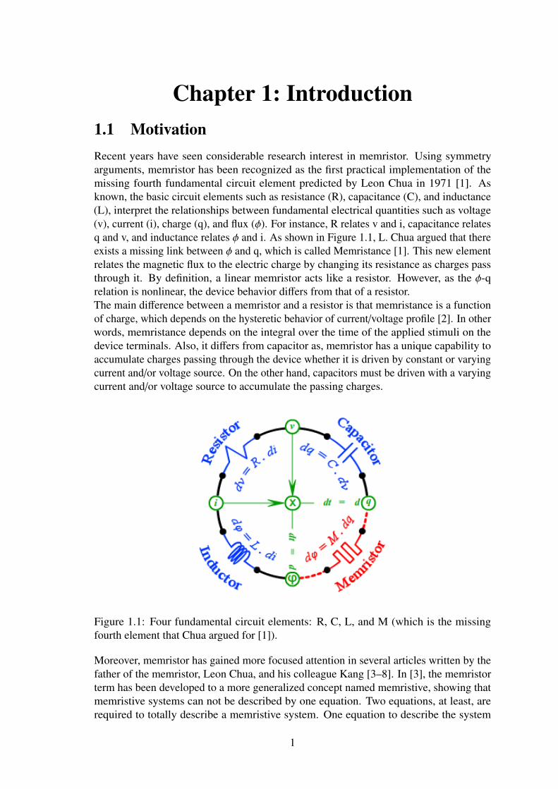
Chapter 1: Introduction1.1 MotivationRecent years have seen considerable research interest in memristor. Using symmetryarguments, memristor has been recognized as the first practical implementation of themissing fourth fundamental circuit element predicted by Leon Chua in 1971 [1]. Asknown, the basic circuit elements such as resistance (R), capacitance (C), and inductance(L), interpret the relationships between fundamental electrical quantities such as voltage(v), current (i), charge (q), and flux (φ). For instance, R relates v and i, capacitance relatesq and v, and inductance relates φ and i. As shown in Figure 1.1, L. Chua argued that thereexists a missing link between φ and q, which is called Memristance [1]. This new elementrelates the magnetic flux to the electric charge by changing its resistance as charges passthrough it. By definition, a linear memristor acts like a resistor. However, as the φ-qrelation is nonlinear, the device behavior differs from that of a resistor.The main difference between a memristor and a resistor is that memristance is a functionof charge, which depends on the hysteretic behavior of current/voltage profile [2]. In otherwords, memristance depends on the integral over the time of the applied stimuli on thedevice terminals. Also, it differs from capacitor as, memristor has a unique capability toaccumulate charges passing through the device whether it is driven by constant or varyingcurrent and/or voltage source. On the other hand, capacitors must be driven with a varyingcurrent and/or voltage source to accumulate the passing charges.
Figure 1.1: Four fundamental circuit elements: R, C, L, and M (which is the missingfourth element that Chua argued for [1]).
Moreover, memristor has gained more focused attention in several articles written by thefather of the memristor, Leon Chua, and his colleague Kang [3–8]. In [3], the memristorterm has been developed to a more generalized concept named memristive, showing thatmemristive systems can not be described by one equation. Two equations, at least, arerequired to totally describe a memristive system. One equation to describe the system
1
memristance and the other one to show how the state variable response to the appliedstimuli. It is also shown that memristors are characterized by a pinched hysteresis loop.The pinched hysteresis loop demonstrates the memristive system response to the appliedfrequency. As shown in Figure 1.2, there is a non-linear dependence on voltage at lowfrequencies, explicit hysteresis at higher frequencies, and hysteresis avalanche at very highfrequencies.
Figure 1.2: Frequency response of Pinched hysteresis loop in memristive systems [3].
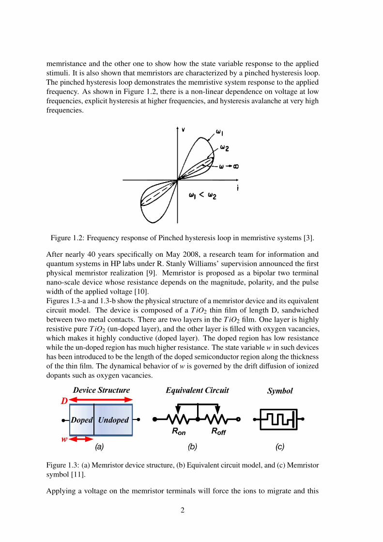
After nearly 40 years specifically on May 2008, a research team for information andquantum systems in HP labs under R. Stanly Williams’ supervision announced the firstphysical memristor realization [9]. Memristor is proposed as a bipolar two terminalnano-scale device whose resistance depends on the magnitude, polarity, and the pulsewidth of the applied voltage [10].Figures 1.3-a and 1.3-b show the physical structure of a memristor device and its equivalentcircuit model. The device is composed of a TiO2 thin film of length D, sandwichedbetween two metal contacts. There are two layers in the TiO2 film. One layer is highlyresistive pure TiO2 (un-doped layer), and the other layer is filled with oxygen vacancies,which makes it highly conductive (doped layer). The doped region has low resistancewhile the un-doped region has much higher resistance. The state variable w in such deviceshas been introduced to be the length of the doped semiconductor region along the thicknessof the thin film. The dynamical behavior of w is governed by the drift diffusion of ionizeddopants such as oxygen vacancies.
Figure 1.3: (a) Memristor device structure, (b) Equivalent circuit model, and (c) Memristorsymbol [11].
Applying a voltage on the memristor terminals will force the ions to migrate and this
2
changes the thickness of the oxygen deficient layer. In other words, when an externalbias voltage, v, is applied across the device, the electric field repels the positively chargedoxygen vacancies in the doped layer into the pure TiO2 layer and the state length w ischanged [11]. Hence, the device total resistivity changes. If the doped region extends tothe full length D (i.e., w/D = 1.0), the total resistivity of the device is dominated by thelow resistivity region, with a value denoted by Ron. On the other hand, when the un-dopedregion extends to the full length D (i.e., w/D = 0), the total resistivity of the device isdominated by the high resistivity region, with a value denoted by Ro f f .Figure 1.3-c displays the memristor symbol. The orientation of the symbol follows theequivalent circuit in 1.3-b, where Ron is at the left and Ro f f is at the right. The polaritymatters in memristor circuits. If a bias condition excites the memristance to increase, thereverse connection of the memristor decreases the memristance, which is equivalent toreversing the polarity of the biasing source [12].The introduction of this new memristor device has revived the research interest in thememristor physical realization. Recently, researchers have proposed several promisingfabrications of the memristor devices based on different materials [13–17]. Beside thesolid state device, magnetic technology may provide the other prospective technologyto build a memristive system. Nanoscale spintronic memristor which depends on spintorque induced magnetization motion and spin transport at semiconductor/ferromagnetjunction had been proposed in [16]. Spintronics take the advantage of the intrinsic spin ofthe electron and its related magnetic moment, besides its fundamental electronic charge insolid-state systems.Spintronic memristor proposed in [17] is an integration between memristive device andspintronic device. In the introduced spin torque memristors [17], the resistance relianceupon the combination of current/voltage is achieved through a mixing of magnetoresistanceand spin torque induced magnetization motion. Based on magnetoresistance principle, theresistance of the submitted spintronic memristor is resolved by its magnetization state.The magnetization state of the device is varied by current electron spin through spin torqueinduced magnetization motion. The total device magnetization state is determined by theintegration effect of electron spin excitations. Therefore, the device resistivity dependsupon the accumulation effects of current/voltage profile.The physical realization of memristors spurred a great interest in the research community.Memristors are considered as one of the possible future alternatives to current CMOStechnology. It is stated by Williams that, memristors can potentially replace the CMOStransistors in the future while providing better performance [18, 19]. Memristor-basedtechnology provides much better scalability and higher utilization [20]. Also, memristorsconsume much less power than transistors as they do not require power to retain state andthey are leakage-free [21]. In addition, the small size of memristors (less than 10nm fortwo terminals memristor) will improve the scalability of integrated circuits significantly.These unique characteristics of memristors give them an important role in shaping thefuture of semiconductors as they possess many advantages over the conventional CMOStransistors. Despite its advantage, memristors face a big challenge on process variationcontrol during the manufacture procedure because of its nano-scale dimensions.In light of its properties and compatibility with CMOS technology , memristors haveattracted many researchers to develop memristor-based applications. Several articles inthe literature have adopted memristors in Programmable Logic Arrays (PLAs) [22–25],
3
and analog circuit applications [26, 27]. The most amazing results have indicated thatapplying a train of periodic pulses to memristor-based electronic circuits makes thesecircuits capable of emulating the brain functions such as learning and anticipating. Suchlearning circuits can be utilized in several applications in various research areas suchas neural networks, fuzzy logic, Neuromorphic applications, and artificial intelligences[28–35]. Also, it can be used in sensors [36], secure communications [37], counters [38],and even more.
1.2 Memory Effects in MemristorThe significance of memory may adopt different concepts in miscellaneous cases. Forexample, when talking about humans, generally it means the act of recalling past expe-riences. In the case of computer, it means the capability to save digital information tobe used in calculations. Actually, looking closer to these two examples, or any othercase where the ”memory” concept is used, leads to realize that all contexts share a com-mon thread that allows a general definition as follows: Memory is the ability to storethe state of a system at a given time, and access such information at another time. Theprocedure of storing such information can be realized in different manners. In the brain,for example, the information seems to be stored in the synapses or connections that areestablished among different neurons via the chemicals that are released when the synapsesare excited by ionic potentials [39]. In the present known memories, it uses a bit ofinformation which may be stored as a charge in a capacitor or transistor gate [40] or as aspin polarization in a certain magnetic materials [41]. In fact, all these examples showthat a memory state is associated with some dynamical properties of the ingredients of theused materials, namely electrons and ions. Actually, a closer look will demonstrate thathistory-dependent particularity is related to how electrons and/or ions rearrange their statein a certain material under the effect of external disturbances. There are different memorytypes: volatile versus nonvolatile; fast versus slow; low capacity versus high capacity; andcheap versus expensive. Nowadays, memory is a part from almost all electronic devicessuch as computers, robots, FPGAs, and so on, which makes the demand on high speedand density memories increased.A number of papers have recently been published [42–44] that have presented chips withboth high speed access and high density. In [42], the authors demonstrated a high-speedSTT-MRAM chip fabricated in 0.13µm CMOS with a read access time of 8ns and writeaccess time of 12ns. In [43], the authors presented a 64Mb STT-MRAM test chip witha 30ns cycle time. Furthermore, in [44], the authors presented an analysis showing howa 1Gb STT-MRAM chip with 10ns read/write access is achievable in todays technology.All of these works have made use of the standard 1 Transistor, 1 Magnetic TunnelingJunction (1T1MTJ) cell. However, current CMOS-based memory technology faces severalhurdles in its pursuit to meet the increasing demand for faster processing and larger datasize. For example, SRAM, the most widely used on-chip memory, due to its fast accesstime and relatively small size, is reaching its physical limits in achieving higher densitiesand lowering power consumption. In addition, the progress in utilizing other emergingmemory technologies, such as EDRAM, MRAM, and PCRAM, slow due to their lack ofcompatibility with CMOS, their slow access time, and their limited scalability.It is stated by Williams that, memristors can potentially replace the CMOS transistors in
4
future application while occupying less chip area, consuming less power, and providingbetter performance [18, 19]. Thus, memristors can play an important role in improvingthe scalability and efficiency of existing memory technology. The nonvolatile advantageof memristors places them as highly ranked candidate for the next generation of universalmemories technology. Memristor-based memories exhibit higher storage density thanhard drives with access times close to those of SRAM memories. It has been declaredthat memristor devices can be scaled down beyond 10nm and memristor-based memoriescan achieve high data storage density close to 100 Gb/cm2, which is higher than currentadvanced flash memory technologies [23, 45]. Several literature makes use of the mim-restor as a digital single bit memory as in [12, 46, 47]. Despite its advantage, readingstored data from the memristor is a challenge. This is due to the accumulative propertyof memristors. So, repeated reading cycles disturb the stored data as in [12, 46, 47] andhence a refreshment circuit is a must.
1.3 Thesis ObjectivesIn this thesis, the physics behind the operation of TiO2 and spintronic memristor arediscussed. Then a comparison between the two devices is introduced based on thisanalysis. Also, an appropriate model from the literature to predict the TiO2 response inmemory cells is explained.On a separate front, novel Read/Write circuits have been introduced to allow the integrationof the memristor device as a memory element. Two of the proposed circuits have theadvantage of non-destructive reading process and eliminate the need of refreshmentdrivers as required by the previous Read/Write circuits such as [12]. Also, the proposedRead/Write circuits exhibit faster access times, less power consumption, and smallerlayout area (i.e., higher storage density) than the circuit introduced in [12]. After that thedynamics of the proposed circuits in an array are tested showing the memory cell responseand the needed power consumption.The contributions of this thesis are the following:
1. Providing a background about memristors.
2. Characterizing and modeling of the TiO2 memristor behavior and spintronics mem-ristor behavior, where a comparison between the two types is submitted.
3. Proposing novel non-destructive Read/Write circuits based on TiO2 memristor.
1.4 Thesis OutlineThe remaining chapters of this thesis are organized as follows:
• Chapter 2 provides a background.
• Chapter 3 describes different types of memristors and provides a comparison be-tween the most promising memristive systems (i.e., TiO2 and spintronic memristor).
• Chapter 4 discusses different memristor applications and shows a literature reviewon Read/Write circuits for memristor based memory cells.
5

• Chapter 5 introduces novel non-destructive Read/Write circuit and compares thesimulation results with previous published results.
• Chapter 6 concludes the thesis and provides the future directions for this work.
6
Chapter 2: Background
Non-Volatile Memory (NVM) devices maintain the data even after removing the powersupply. Magnetic tapes, floppy disks, optical disks, and flash memories are classified asNVM devices. For the time being, solid-state based NVM devices like flash memories havebecome the most common media for storing the data. Generally, Solid-State NVM deviceshave a small footprint, large storage capacity, low power consumption, low latency, andvery good rugged properties that make them the best storage media for portable devices.Unlike other NVM devices (i.e., magnetic and optical storage devices), the solid-statememories do not require the physical movement of the read head to attain the segmentwhere the data is stored as what has happened in magnetic and optical storage systems andhence the read and write operations in these systems (i.e., solid-state storage systems) aremuch faster. On the other side, and similar to the magnetic and optical memory devices,solid-state NVM devices store the data without needing power to maintain the data.
Despite its advantages, current NVM technologies are much slower than volatile ones(like Random Access Memory (RAM)), which makes NVM devices not suitable for veryfast data access applications like processor cache memory (i.e., Static Random AccessMemory (SRAM)) or computers’ main memory (i.e., Dynamic Random Access Memory(DRAM)). However, they introduce better speed advantage than other non-volatile devices(i.e., hard disk and optical devices). Referring to the International Technology Roadmap forSemiconductors (ITRS) report (ITRS 2007) [48], it is assumed that, by 2019, 16nm half-pitch non-volatile memory cells will provide a capacity of around 46Gb/cm2, assuming100 per cent area efficiency.
Nevertheless, current memory technologies have limitations which are inconsistentwith new technologies (i.e., Digital cameras, Mobile phones, and Computers) where higherstorage capacity, faster access time, lower power consumption, and less cost are highlyrequired. Based on Moore’s law, and as shown in Figure 2.1, the number of transistorsper chip doubled every 18 months approximately [49, 50]. But the trend of depletedelectronics and the need for higher storage capacity shows that Moore’s law is not enoughand more Moore or even more than Moore is needed as displayed in Figure 2.2 [51].
Therefore, new non-volatile memory technologies like Phase Change Random AccessMemory (PCRAM), Resistive Random Access Memory (RRAM), Magnetoresistive Ran-dom Access Memory (MRAM), and Ferroelectric Random Access Memory (FERAM)were introduced to replace the well known NVM technology.
2.1 Emerging Non-Volatile Memory Technology
To reduce the gap between what is needed from memories and what present memorytechnologies offer, new non-volatile memory (NVM) technologies had been put underresearch. Most of these technologies are in different phases of realization. Some are still inpremature research stages, others have working prototypes, and some of them are alreadyentering into commercial manufacturing.
7
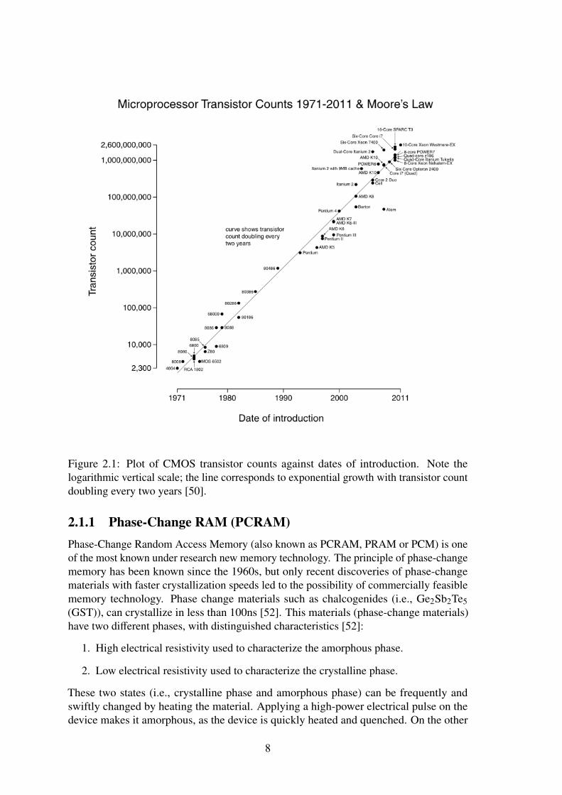
Figure 2.1: Plot of CMOS transistor counts against dates of introduction. Note thelogarithmic vertical scale; the line corresponds to exponential growth with transistor countdoubling every two years [50].
2.1.1 Phase-Change RAM (PCRAM)Phase-Change Random Access Memory (also known as PCRAM, PRAM or PCM) is oneof the most known under research new memory technology. The principle of phase-changememory has been known since the 1960s, but only recent discoveries of phase-changematerials with faster crystallization speeds led to the possibility of commercially feasiblememory technology. Phase change materials such as chalcogenides (i.e., Ge2Sb2Te5(GST)), can crystallize in less than 100ns [52]. This materials (phase-change materials)have two different phases, with distinguished characteristics [52]:
1. High electrical resistivity used to characterize the amorphous phase.
2. Low electrical resistivity used to characterize the crystalline phase.
These two states (i.e., crystalline phase and amorphous phase) can be frequently andswiftly changed by heating the material. Applying a high-power electrical pulse on thedevice makes it amorphous, as the device is quickly heated and quenched. On the other
8
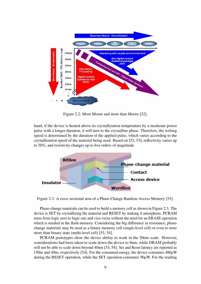
Figure 2.2: More Moore and more than Moore [52].
hand, if the device is heated above its crystallization temperature by a moderate powerpulse with a longer duration, it will turn to the crystalline phase. Therefore, the writingspeed is determined by the duration of the applied pulse, which varies according to thecrystallization speed of the material being used. Based on [52, 53], reflectivity varies upto 30%, and resistivity changes up to five orders of magnitude.
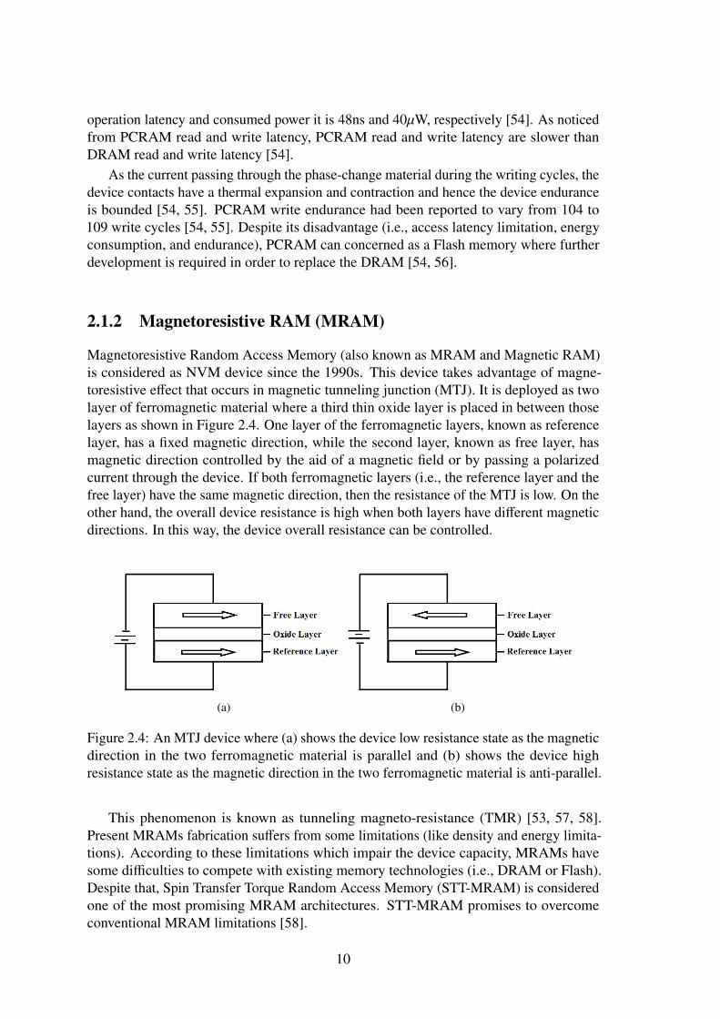
Figure 2.3: A cross sectional area of a Phase-Change Random Access Memory [53].
Phase-change materials can be used to build a memory cell as shown in Figure 2.3. Thedevice is SET by crystallizing the material and RESET by making it amorphous. PCRAMturns from logic zero to logic one and vice-versa without the need for an ERASE operationwhich is needed in the flash memory. Considering the big difference in resistance, phase-change materials may be used as a binary memory cell (single-level cell) or even to storemore than binary state (multi-level cell) [53, 54].
PCRAM prototypes show the device ability to work in the 20nm scale. However,considerations had been taken to scale down the device to 9nm, while DRAM probablywill not be able to scale down beyond 40nm [53, 54]. Set and Reset latency are reported as150ns and 40ns, respectively [54]. For the consumed energy, the device consumes 480µWduring the RESET operation, while the SET operation consumes 90µW. For the reading
9
operation latency and consumed power it is 48ns and 40µW, respectively [54]. As noticedfrom PCRAM read and write latency, PCRAM read and write latency are slower thanDRAM read and write latency [54].
As the current passing through the phase-change material during the writing cycles, thedevice contacts have a thermal expansion and contraction and hence the device enduranceis bounded [54, 55]. PCRAM write endurance had been reported to vary from 104 to109 write cycles [54, 55]. Despite its disadvantage (i.e., access latency limitation, energyconsumption, and endurance), PCRAM can concerned as a Flash memory where furtherdevelopment is required in order to replace the DRAM [54, 56].
2.1.2 Magnetoresistive RAM (MRAM)
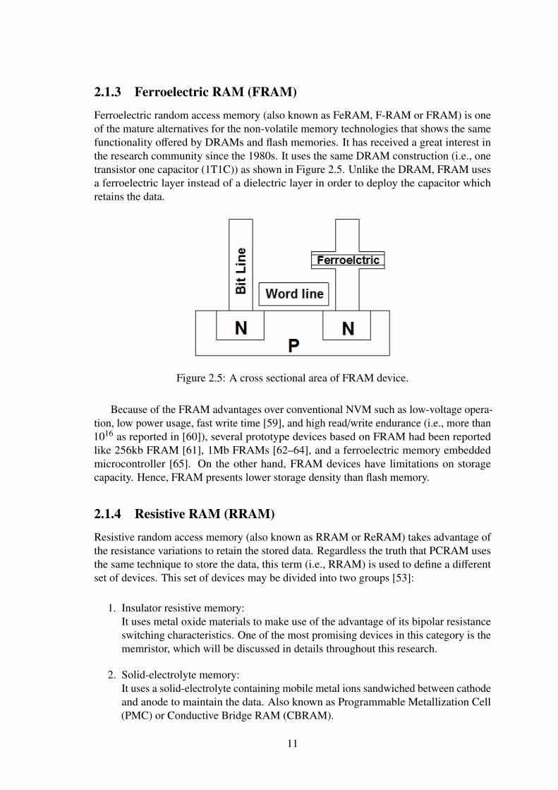
Magnetoresistive Random Access Memory (also known as MRAM and Magnetic RAM)is considered as NVM device since the 1990s. This device takes advantage of magne-toresistive effect that occurs in magnetic tunneling junction (MTJ). It is deployed as twolayer of ferromagnetic material where a third thin oxide layer is placed in between thoselayers as shown in Figure 2.4. One layer of the ferromagnetic layers, known as referencelayer, has a fixed magnetic direction, while the second layer, known as free layer, hasmagnetic direction controlled by the aid of a magnetic field or by passing a polarizedcurrent through the device. If both ferromagnetic layers (i.e., the reference layer and thefree layer) have the same magnetic direction, then the resistance of the MTJ is low. On theother hand, the overall device resistance is high when both layers have different magneticdirections. In this way, the device overall resistance can be controlled.
(a) (b)
Figure 2.4: An MTJ device where (a) shows the device low resistance state as the magneticdirection in the two ferromagnetic material is parallel and (b) shows the device highresistance state as the magnetic direction in the two ferromagnetic material is anti-parallel.
This phenomenon is known as tunneling magneto-resistance (TMR) [53, 57, 58].Present MRAMs fabrication suffers from some limitations (like density and energy limita-tions). According to these limitations which impair the device capacity, MRAMs havesome difficulties to compete with existing memory technologies (i.e., DRAM or Flash).Despite that, Spin Transfer Torque Random Access Memory (STT-MRAM) is consideredone of the most promising MRAM architectures. STT-MRAM promises to overcomeconventional MRAM limitations [58].
10
2.1.3 Ferroelectric RAM (FRAM)
Ferroelectric random access memory (also known as FeRAM, F-RAM or FRAM) is oneof the mature alternatives for the non-volatile memory technologies that shows the samefunctionality offered by DRAMs and flash memories. It has received a great interest inthe research community since the 1980s. It uses the same DRAM construction (i.e., onetransistor one capacitor (1T1C)) as shown in Figure 2.5. Unlike the DRAM, FRAM usesa ferroelectric layer instead of a dielectric layer in order to deploy the capacitor whichretains the data.
Figure 2.5: A cross sectional area of FRAM device.
Because of the FRAM advantages over conventional NVM such as low-voltage opera-tion, low power usage, fast write time [59], and high read/write endurance (i.e., more than1016 as reported in [60]), several prototype devices based on FRAM had been reportedlike 256kb FRAM [61], 1Mb FRAMs [62–64], and a ferroelectric memory embeddedmicrocontroller [65]. On the other hand, FRAM devices have limitations on storagecapacity. Hence, FRAM presents lower storage density than flash memory.
2.1.4 Resistive RAM (RRAM)
Resistive random access memory (also known as RRAM or ReRAM) takes advantage ofthe resistance variations to retain the stored data. Regardless the truth that PCRAM usesthe same technique to store the data, this term (i.e., RRAM) is used to define a differentset of devices. This set of devices may be divided into two groups [53]:
1. Insulator resistive memory:It uses metal oxide materials to make use of the advantage of its bipolar resistanceswitching characteristics. One of the most promising devices in this category is thememristor, which will be discussed in details throughout this research.
2. Solid-electrolyte memory:It uses a solid-electrolyte containing mobile metal ions sandwiched between cathodeand anode to maintain the data. Also known as Programmable Metallization Cell(PMC) or Conductive Bridge RAM (CBRAM).
11
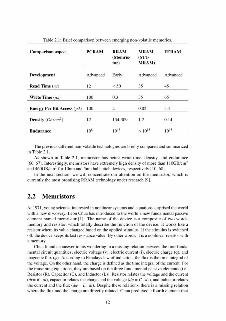
Table 2.1: Brief comparison between emerging non-volatile memories.
Comparison aspect PCRAM RRAM(Memris-tor)
MRAM(STT-MRAM)
FERAM
Development Advanced Early Advanced Advanced
Read Time (ns) 12 < 50 35 45
Write Time (ns) 100 0.3 35 65
Energy Per Bit Access (pJ) 100 2 0.02 3.4
Density (Gb/cm2) 12 154-309 1.2 0.14
Endurance 108 1015 > 1015 1015
The previous different non-volatile technologies are briefly compared and summarizedin Table 2.1.
As shown in Table 2.1, memristor has better write time, density, and endurance[66, 67]. Interestingly, memristors have extremely high density of more than 110GB/cm2
and 460GB/cm2 for 10nm and 5nm half-pitch devices, respectively [10, 68].In the next section, we will concentrate our attention on the memristor, which is
currently the most promising RRAM technology under research [9].
2.2 Memristors
At 1971, young scientist interested in nonlinear systems and equations surprised the worldwith a new discovery. Leon Chua has introduced to the world a new fundamental passiveelement named memristor [1]. The name of the device is a composite of two words,memory and resistor, which totally describe the function of the device. It works like aresistor where its value changed based on the applied stimulus. If the stimulus is switchedoff, the device keeps its last resistance value. By other words, it is a nonlinear resistor witha memory.
Chua found an answer to his wondering in a missing relation between the four funda-mental circuit quantities; electric voltage (v), electric current (i), electric charge (q), andmagnetic flux (ϕ). According to Faradays law of induction, the flux is the time integral ofthe voltage. On the other hand, the charge is defined as the time integral of the current. Forthe remaining equations, they are based on the three fundamental passive elements (i.e.,Resistor (R), Capacitor (C), and Inductor (L)). Resistor relates the voltage and the current(dv= R . di), capacitor relates the charge and the voltage (dq = C . dv), and inductor relatesthe current and the flux (dϕ = L . di). Despite these relations, there is a missing relationwhere the flux and the charge are directly related. Chua predicted a fourth element that
12
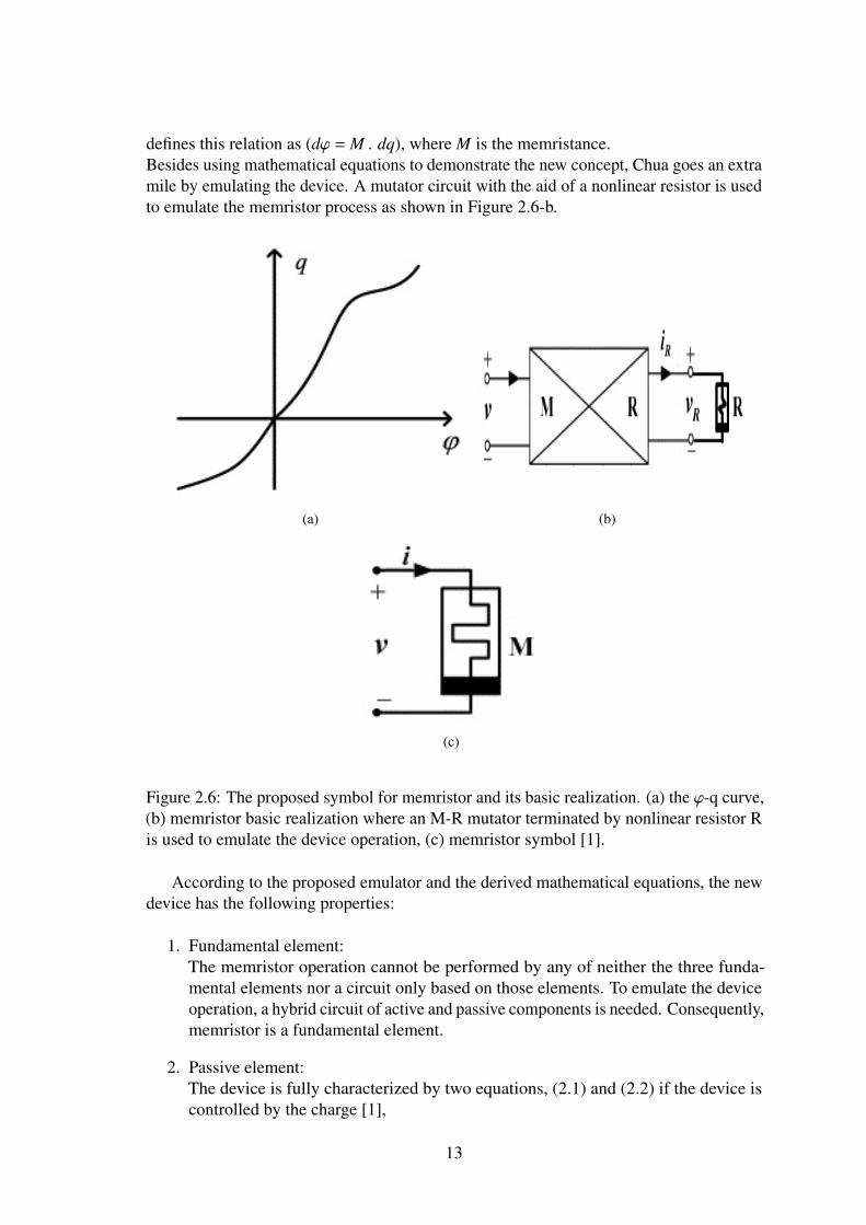
defines this relation as (dϕ = M . dq), where M is the memristance.Besides using mathematical equations to demonstrate the new concept, Chua goes an extramile by emulating the device. A mutator circuit with the aid of a nonlinear resistor is usedto emulate the memristor process as shown in Figure 2.6-b.
(a) (b)
(c)
Figure 2.6: The proposed symbol for memristor and its basic realization. (a) the ϕ-q curve,(b) memristor basic realization where an M-R mutator terminated by nonlinear resistor Ris used to emulate the device operation, (c) memristor symbol [1].
According to the proposed emulator and the derived mathematical equations, the newdevice has the following properties:
1. Fundamental element:The memristor operation cannot be performed by any of neither the three funda-mental elements nor a circuit only based on those elements. To emulate the deviceoperation, a hybrid circuit of active and passive components is needed. Consequently,memristor is a fundamental element.
2. Passive element:The device is fully characterized by two equations, (2.1) and (2.2) if the device iscontrolled by the charge [1],
13
v(t) = M(q(t))× i(t) (2.1)
M(q) = dϕ(q)/dq (2.2)
where, M(q) is the memristance, v is the applied voltage, and i is the current passingthrough the device; or described by (2.3) and (2.4), if it is controlled by the flux [1],
i(t) = G(ϕ(t))× v(t) (2.3)
G(ϕ) = dq(ϕ)/dϕ (2.4)
where, G(ϕ) is the memductance. So, the instantaneous power (p) is characterizedby,
p(t) = v(t)× i(t) = M(q(t))× [i(t)]2 (2.5)
Thus, the device is considered a passive element if and only if M(q) ≥ 0, which isthe only solution of the device according to the ϕ-q curve (shown in Figure 2.6-a)that describes the device. In other words, the device is incapable of energy gain orconsumption.
3. Analog device:Memristor has a unique signal processing characteristic, where the memristanceis depending on the time integral of the current passing through the device or thevoltage applied on the device terminals. So, memristance is a time varying quantitywhich depends on the total net charge over the time. This dependency gives thedevice its analogy criteria.
4. Nonlinear criterion:Based on linear system definition, the system variable, which is in this case thememristance, can be written or solved by a linear combination of independentcomponents, or in other words the system has a certain output for a certain input.Based on (2.2) and (2.4), memristance depends on the ϕ-q relation and the timeintegral of stimuli (voltage and current), where the linearity principle cannot beapplied.
5. Stimuli dependence:Memristance value depends on the applied stimuli (voltage or current) regardlessof the source shape. This fact comes from the device unique signal processingproperty. The only thing that matters is the net applied injection and the period ofthis injection.Due to the integration of the applied segments done by the device, the source shape(e.g., triangle, pulse, or sine wave) does not make any difference but only the appliednet charge counts.
14
An electromagnetic commentary of memristor properties is supplied to ratification ofthe possibility of finding such a device. Also Chua applies some theorem like Closuretheorem and Existence and Uniqueness theorem to prove the possibility of inventing sucha device.Besides the aforementioned, some uninhabitable applications are submitted like modelingan amorphous ovonic threshold switch, modeling an electrolytic E-cell, and signal pro-cessing application (e.g., generating a staircase waveform).Later, Chua and Kang expand the definition of the memristor to a more general definitionnamed memristive system [3]. According to the new definition, some systems and devicesare considered as special cases of memristive systems such as thermistors, discharge tubes,and ionic systems described by Hodgkin-Huxley circuit model [3]. Even new generalequations, that fully describe the memristive systems, are introduced as
x = f (x,u, t) (2.6)
y = g(x,u, t) u (2.7)
where, u and y are the input and output of the system respectively, x is the state of thesystem, and t is the time. If the current (i) and the voltage (v) define the input (u) and theoutput (y) of the system respectively, then a memristive system is represented by
x = f (x, i, t) (2.8)
y = R(x, i, t)× i (2.9)
where, R represents the system resistivity.Besides the above mentioned properties and based on the new analysis, some new
properties were added,
6. I-V Characteristic curve:The memristive system I-V characteristic curve under periodic stimulus is repre-sented by a double valued Lissajous figure, where any value of the current (i) has atmost two distinct values of the voltage (v) and the figure is symmetric hysteresisaround the origin [3] as shown in Figure 2.7.Thus, applying a current source
i(t) = Icosωt (2.10)
where, I is the current passing through the device and ω is the frequency, will causetwo corresponding voltage values (v1 and v2) for each current value (i) dependingon the passing current direction. Assume the system has a low memristance valueand a positive current is passing through it, then the system will have low voltagedrop (v1). On the other hand, if the system memristance is maximum and the samecurrent magnitude is passing in the reverse direction, the system will have largevoltage drop (v2).
According to the I-V curve symmetry, there will be two equally resistive value (R(x,i) = R(x,-i) ) under the same periodic current source.
15
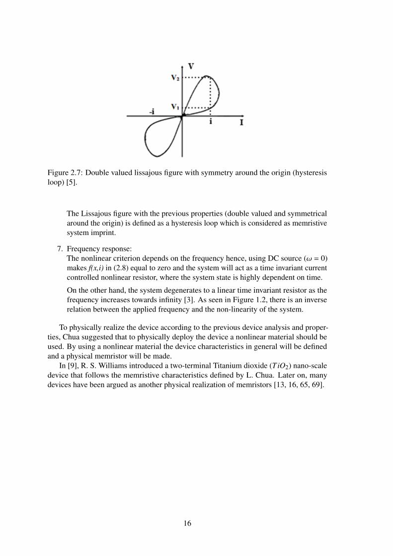
Figure 2.7: Double valued lissajous figure with symmetry around the origin (hysteresisloop) [5].
The Lissajous figure with the previous properties (double valued and symmetricalaround the origin) is defined as a hysteresis loop which is considered as memristivesystem imprint.
7. Frequency response:The nonlinear criterion depends on the frequency hence, using DC source (ω = 0)makes f(x,i) in (2.8) equal to zero and the system will act as a time invariant currentcontrolled nonlinear resistor, where the system state is highly dependent on time.
On the other hand, the system degenerates to a linear time invariant resistor as thefrequency increases towards infinity [3]. As seen in Figure 1.2, there is an inverserelation between the applied frequency and the non-linearity of the system.
To physically realize the device according to the previous device analysis and proper-ties, Chua suggested that to physically deploy the device a nonlinear material should beused. By using a nonlinear material the device characteristics in general will be definedand a physical memristor will be made.
In [9], R. S. Williams introduced a two-terminal Titanium dioxide (TiO2) nano-scaledevice that follows the memristive characteristics defined by L. Chua. Later on, manydevices have been argued as another physical realization of memristors [13, 16, 65, 69].
16
Chapter 3: Memristive SystemsRecently, after the announcement of HP’s memristor, memristive systems gained a greatinterest where many systems show memristive behavior are introduced. These systemshave different memristance mechanisms like thermal effects, chemical reactions, ionictransfer, spin polarization, and phase transitions. Some of these systems were earlyintroduced in [3] (i.e., thermistors and ionic systems). Other systems were studied duringthe last 10-15 years for the sake of resistive-switching memory development. Resistive-Switching memory research began in 1962 when Hickmott observed a hysteresis behaviorin oxide insulators [70]. After that, Simmons and Verderber examined the resistanceswitching mechanism in thin silicon monoxide (SiO) film sandwiched between two metalelectrodes [71]. It was also tested in TiO2 devices by Argall [72]. However, resistiveswitching devices were not recognized as memristive systems until 2008 [9]. After thatother memristive systems such as spintronic devices [17, 20], phase-transition materials[73, 74] and polaronic systems [75] were introduced. Below, memristive properties of avariety of physical memristive systems are discussed.
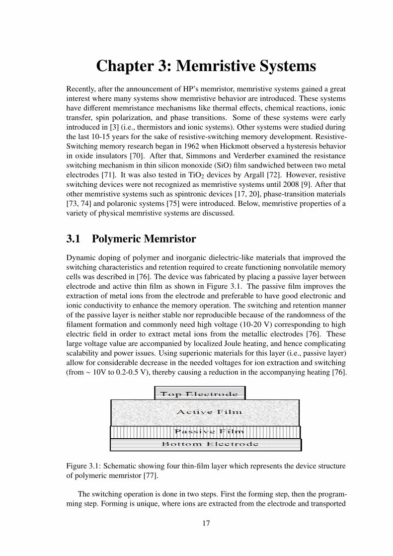
3.1 Polymeric MemristorDynamic doping of polymer and inorganic dielectric-like materials that improved theswitching characteristics and retention required to create functioning nonvolatile memorycells was described in [76]. The device was fabricated by placing a passive layer betweenelectrode and active thin film as shown in Figure 3.1. The passive film improves theextraction of metal ions from the electrode and preferable to have good electronic andionic conductivity to enhance the memory operation. The switching and retention mannerof the passive layer is neither stable nor reproducible because of the randomness of thefilament formation and commonly need high voltage (10-20 V) corresponding to highelectric field in order to extract metal ions from the metallic electrodes [76]. Theselarge voltage value are accompanied by localized Joule heating, and hence complicatingscalability and power issues. Using superionic materials for this layer (i.e., passive layer)allow for considerable decrease in the needed voltages for ion extraction and switching(from ∼ 10V to 0.2-0.5 V), thereby causing a reduction in the accompanying heating [76].
Figure 3.1: Schematic showing four thin-film layer which represents the device structureof polymeric memristor [77].
The switching operation is done in two steps. First the forming step, then the program-ming step. Forming is unique, where ions are extracted from the electrode and transported
17
or injected into the active layer. In the second step, a conductive bridge is formed andthen broken in a repetitive manner (representing programming and erasing operations) inresponse to the applied electric field [76].
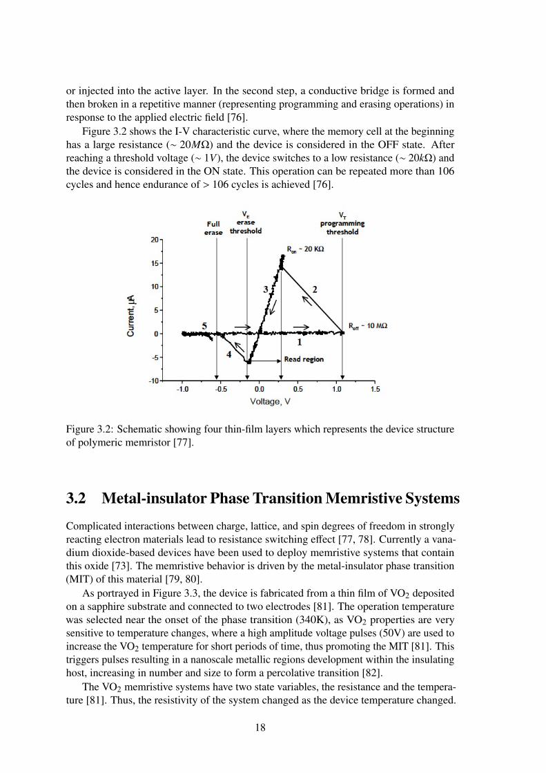
Figure 3.2 shows the I-V characteristic curve, where the memory cell at the beginninghas a large resistance (∼ 20MΩ) and the device is considered in the OFF state. Afterreaching a threshold voltage (∼ 1V), the device switches to a low resistance (∼ 20kΩ) andthe device is considered in the ON state. This operation can be repeated more than 106cycles and hence endurance of > 106 cycles is achieved [76].
Figure 3.2: Schematic showing four thin-film layers which represents the device structureof polymeric memristor [77].
3.2 Metal-insulator Phase Transition Memristive Systems
Complicated interactions between charge, lattice, and spin degrees of freedom in stronglyreacting electron materials lead to resistance switching effect [77, 78]. Currently a vana-dium dioxide-based devices have been used to deploy memristive systems that containthis oxide [73]. The memristive behavior is driven by the metal-insulator phase transition(MIT) of this material [79, 80].
As portrayed in Figure 3.3, the device is fabricated from a thin film of VO2 depositedon a sapphire substrate and connected to two electrodes [81]. The operation temperaturewas selected near the onset of the phase transition (340K), as VO2 properties are verysensitive to temperature changes, where a high amplitude voltage pulses (50V) are used toincrease the VO2 temperature for short periods of time, thus promoting the MIT [81]. Thistriggers pulses resulting in a nanoscale metallic regions development within the insulatinghost, increasing in number and size to form a percolative transition [82].
The VO2 memristive systems have two state variables, the resistance and the tempera-ture [81]. Thus, the resistivity of the system changed as the device temperature changed.
18
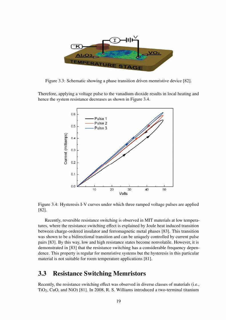
Figure 3.3: Schematic showing a phase transition driven memristive device [82].
Therefore, applying a voltage pulse to the vanadium dioxide results in local heating andhence the system resistance decreases as shown in Figure 3.4.
Figure 3.4: Hysteresis I-V curves under which three ramped voltage pulses are applied[82].
Recently, reversible resistance switching is observed in MIT materials at low tempera-tures, where the resistance switching effect is explained by Joule heat induced transitionbetween charge-ordered insulator and ferromagnetic metal phases [83]. This transitionwas shown to be a bidirectional transition and can be uniquely controlled by current pulsepairs [83]. By this way, low and high resistance states become nonvolatile. However, it isdemonstrated in [83] that the resistance switching has a considerable frequency depen-dence. This property is regular for memristive systems but the hysteresis in this particularmaterial is not suitable for room temperature applications [81].
3.3 Resistance Switching MemristorsRecently, the resistance switching effect was observed in diverse classes of materials (i.e.,TiO2, CuO, and NiO) [81]. In 2008, R. S. Williams introduced a two-terminal titanium
19
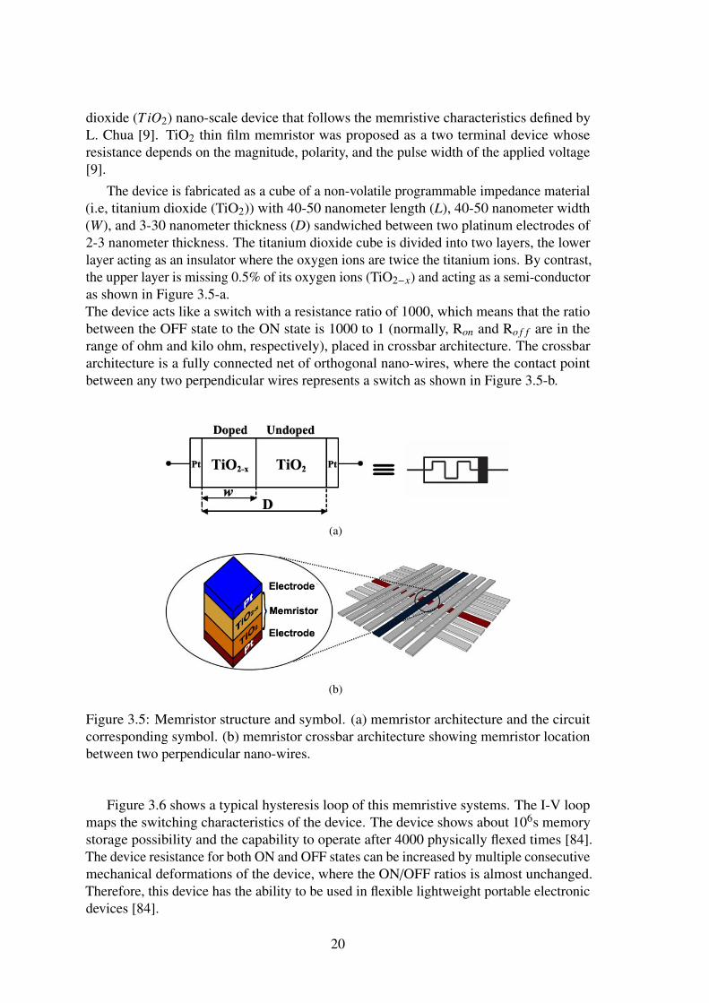
dioxide (TiO2) nano-scale device that follows the memristive characteristics defined byL. Chua [9]. TiO2 thin film memristor was proposed as a two terminal device whoseresistance depends on the magnitude, polarity, and the pulse width of the applied voltage[9].
The device is fabricated as a cube of a non-volatile programmable impedance material(i.e, titanium dioxide (TiO2)) with 40-50 nanometer length (L), 40-50 nanometer width(W), and 3-30 nanometer thickness (D) sandwiched between two platinum electrodes of2-3 nanometer thickness. The titanium dioxide cube is divided into two layers, the lowerlayer acting as an insulator where the oxygen ions are twice the titanium ions. By contrast,the upper layer is missing 0.5% of its oxygen ions (TiO2−x) and acting as a semi-conductoras shown in Figure 3.5-a.The device acts like a switch with a resistance ratio of 1000, which means that the ratiobetween the OFF state to the ON state is 1000 to 1 (normally, Ron and Ro f f are in therange of ohm and kilo ohm, respectively), placed in crossbar architecture. The crossbararchitecture is a fully connected net of orthogonal nano-wires, where the contact pointbetween any two perpendicular wires represents a switch as shown in Figure 3.5-b.
(a)
(b)
Figure 3.5: Memristor structure and symbol. (a) memristor architecture and the circuitcorresponding symbol. (b) memristor crossbar architecture showing memristor locationbetween two perpendicular nano-wires.
Figure 3.6 shows a typical hysteresis loop of this memristive systems. The I-V loopmaps the switching characteristics of the device. The device shows about 106s memorystorage possibility and the capability to operate after 4000 physically flexed times [84].The device resistance for both ON and OFF states can be increased by multiple consecutivemechanical deformations of the device, where the ON/OFF ratios is almost unchanged.Therefore, this device has the ability to be used in flexible lightweight portable electronicdevices [84].
20
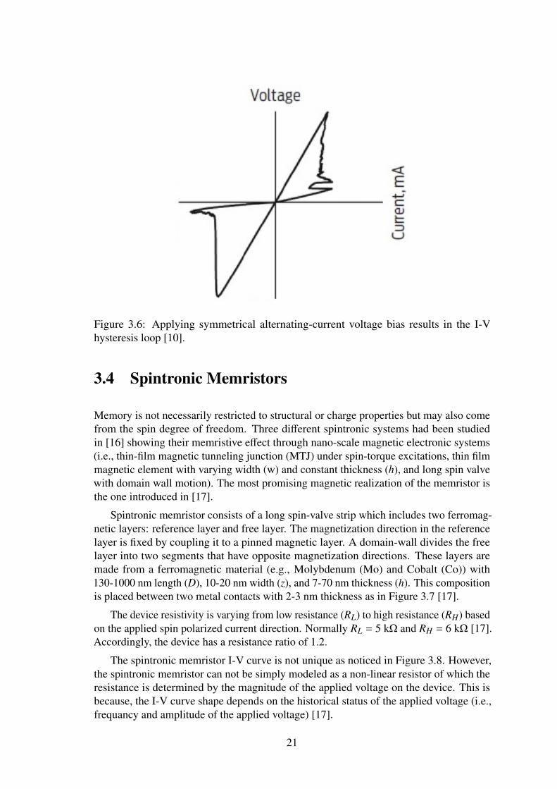
Figure 3.6: Applying symmetrical alternating-current voltage bias results in the I-Vhysteresis loop [10].
3.4 Spintronic Memristors
Memory is not necessarily restricted to structural or charge properties but may also comefrom the spin degree of freedom. Three different spintronic systems had been studiedin [16] showing their memristive effect through nano-scale magnetic electronic systems(i.e., thin-film magnetic tunneling junction (MTJ) under spin-torque excitations, thin filmmagnetic element with varying width (w) and constant thickness (h), and long spin valvewith domain wall motion). The most promising magnetic realization of the memristor isthe one introduced in [17].
Spintronic memristor consists of a long spin-valve strip which includes two ferromag-netic layers: reference layer and free layer. The magnetization direction in the referencelayer is fixed by coupling it to a pinned magnetic layer. A domain-wall divides the freelayer into two segments that have opposite magnetization directions. These layers aremade from a ferromagnetic material (e.g., Molybdenum (Mo) and Cobalt (Co)) with130-1000 nm length (D), 10-20 nm width (z), and 7-70 nm thickness (h). This compositionis placed between two metal contacts with 2-3 nm thickness as in Figure 3.7 [17].
The device resistivity is varying from low resistance (RL) to high resistance (RH) basedon the applied spin polarized current direction. Normally RL = 5 kΩ and RH = 6 kΩ [17].Accordingly, the device has a resistance ratio of 1.2.
The spintronic memristor I-V curve is not unique as noticed in Figure 3.8. However,the spintronic memristor can not be simply modeled as a non-linear resistor of which theresistance is determined by the magnitude of the applied voltage on the device. This isbecause, the I-V curve shape depends on the historical status of the applied voltage (i.e.,frequancy and amplitude of the applied voltage) [17].
21
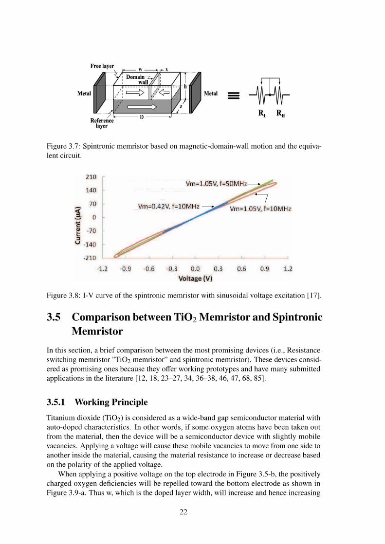
Figure 3.7: Spintronic memristor based on magnetic-domain-wall motion and the equiva-lent circuit.
Figure 3.8: I-V curve of the spintronic memristor with sinusoidal voltage excitation [17].
3.5 Comparison between TiO2 Memristor and SpintronicMemristor
In this section, a brief comparison between the most promising devices (i.e., Resistanceswitching memristor ”TiO2 memristor” and spintronic memristor). These devices consid-ered as promising ones because they offer working prototypes and have many submittedapplications in the literature [12, 18, 23–27, 34, 36–38, 46, 47, 68, 85].
3.5.1 Working PrincipleTitanium dioxide (TiO2) is considered as a wide-band gap semiconductor material withauto-doped characteristics. In other words, if some oxygen atoms have been taken outfrom the material, then the device will be a semiconductor device with slightly mobilevacancies. Applying a voltage will cause these mobile vacancies to move from one side toanother inside the material, causing the material resistance to increase or decrease basedon the polarity of the applied voltage.
When applying a positive voltage on the top electrode in Figure 3.5-b, the positivelycharged oxygen deficiencies will be repelled toward the bottom electrode as shown inFigure 3.9-a. Thus w, which is the doped layer width, will increase and hence increasing
22
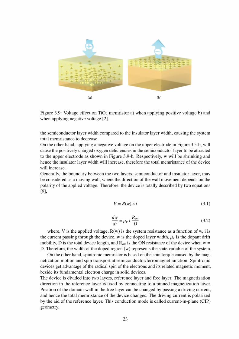
(a) (b)
Figure 3.9: Voltage effect on TiO2 memristor a) when applying positive voltage b) andwhen applying negative voltage [2].
the semiconductor layer width compared to the insulator layer width, causing the systemtotal memristance to decrease.On the other hand, applying a negative voltage on the upper electrode in Figure 3.5-b, willcause the positively charged oxygen deficiencies in the semiconductor layer to be attractedto the upper electrode as shown in Figure 3.9-b. Respectively, w will be shrinking andhence the insulator layer width will increase, therefore the total memristance of the devicewill increase.Generally, the boundary between the two layers, semiconductor and insulator layer, maybe considered as a moving wall, where the direction of the wall movement depends on thepolarity of the applied voltage. Therefore, the device is totally described by two equations[9],
V = R(w)× i (3.1)
dwdt
= µv iRon
D(3.2)
where, V is the applied voltage, R(w) is the system resistance as a function of w, i isthe current passing through the device, w is the doped layer width, µv is the dopant driftmobility, D is the total device length, and Ron is the ON resistance of the device when w =
D. Therefore, the width of the doped region (w) represents the state variable of the system.On the other hand, spintronic memristor is based on the spin torque caused by the mag-
netization motion and spin transport at semiconductor/ferromagnet junction. Spintronicdevices get advantage of the radical spin of the electrons and its related magnetic moment,beside its fundamental electron charge in solid devices.The device is divided into two layers, reference layer and free layer. The magnetizationdirection in the reference layer is fixed by connecting to a pinned magnetization layer.Position of the domain-wall in the free layer can be changed by passing a driving current,and hence the total memristance of the device changes. The driving current is polarizedby the aid of the reference layer. This conduction mode is called current-in-plane (CIP)geometry.
23
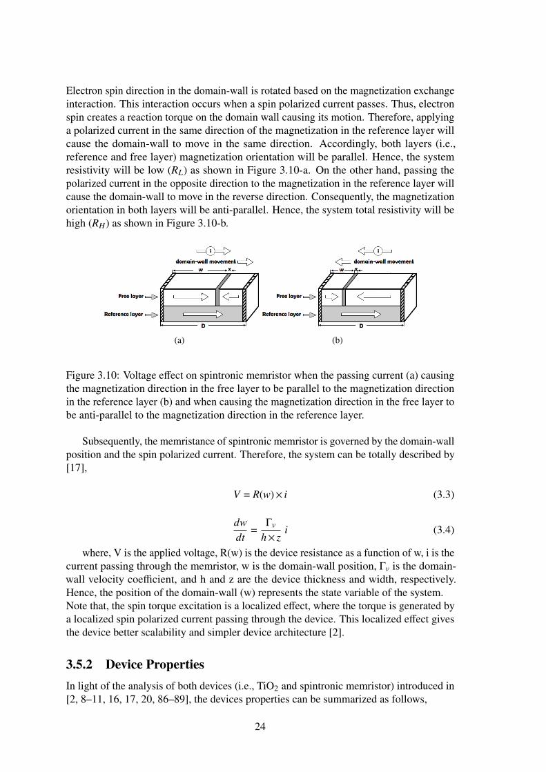
Electron spin direction in the domain-wall is rotated based on the magnetization exchangeinteraction. This interaction occurs when a spin polarized current passes. Thus, electronspin creates a reaction torque on the domain wall causing its motion. Therefore, applyinga polarized current in the same direction of the magnetization in the reference layer willcause the domain-wall to move in the same direction. Accordingly, both layers (i.e.,reference and free layer) magnetization orientation will be parallel. Hence, the systemresistivity will be low (RL) as shown in Figure 3.10-a. On the other hand, passing thepolarized current in the opposite direction to the magnetization in the reference layer willcause the domain-wall to move in the reverse direction. Consequently, the magnetizationorientation in both layers will be anti-parallel. Hence, the system total resistivity will behigh (RH) as shown in Figure 3.10-b.
(a) (b)
Figure 3.10: Voltage effect on spintronic memristor when the passing current (a) causingthe magnetization direction in the free layer to be parallel to the magnetization directionin the reference layer (b) and when causing the magnetization direction in the free layer tobe anti-parallel to the magnetization direction in the reference layer.
Subsequently, the memristance of spintronic memristor is governed by the domain-wallposition and the spin polarized current. Therefore, the system can be totally described by[17],
V = R(w)× i (3.3)
dwdt
=Γv
h× zi (3.4)
where, V is the applied voltage, R(w) is the device resistance as a function of w, i is thecurrent passing through the memristor, w is the domain-wall position, Γv is the domain-wall velocity coefficient, and h and z are the device thickness and width, respectively.Hence, the position of the domain-wall (w) represents the state variable of the system.Note that, the spin torque excitation is a localized effect, where the torque is generated bya localized spin polarized current passing through the device. This localized effect givesthe device better scalability and simpler device architecture [2].
3.5.2 Device PropertiesIn light of the analysis of both devices (i.e., TiO2 and spintronic memristor) introduced in[2, 8–11, 16, 17, 20, 86–89], the devices properties can be summarized as follows,
24
1. Nano-scale deviceTitanium dioxide is a well known material for decades, but no one thought aboutit as a non-volatile programmable impedance material because of the high electricfield needed to move the oxygen atom for a sensible distance even in the micro scaledevices. The oxygen atom slowness may be the reason of this issue. But because ofthe device nano-scale, the oxygen atoms will be free to move inside the device witha sensible rate, where the device resistance changed according to this movement.Accordingly, getting smaller getting better as the device characteristics are enhanced(e.g., faster response time and lower applied voltage).
For spintronic devices, they are typically fabricated in the sub-micron scale. Ac-cording to the device fabrication in nano-scale, memristive effect of the device hasshown up. But it is worth mentioning that, the device scaling down has lengthlimitation which can not be exceeded. The domain-wall thickness (x) is one of theselimitations. Also, the macroscopic nature of the magnetic devices makes it hard tobe scaled down. This is because if there is a single defect in the device structure, alarge amount of bits is rendered unusable [2].
2. Bipolar deviceBased on the previous discussion, memristor state, for both TiO2 and spintronic, isdepending on the polarity of the applied voltage and hence the device memristance.
3. Great resiliency and reliability when power is interruptedMemristors store data as resistance. This resistance depends on the oxygen atoms’movement in TiO2 memristors or the electron spin and magnetization direction inspintronic memristors caused by the applied stimulus. Thus if this stimulus is turnedoff, the oxygen atoms’ position or magnetization direction will save its last position.So, if a memory device is made totally from memristors (i.e., memory cells, memoryarray peripherals, and sense amplifiers), then cutting off the power does not matteras the device will save its last state until the power is restored and hence the devicehas a better reliability.
4. Memristance considerationMigration between doped region low resistance and un-doped region high resistancein TiO2 represents the system resistivity, named memristance, as,
R(w) = Ro f f −(Ro f f −Ron) w
D(3.5)
where, Ro f f is the device resistance when w = zero. Because of the device non-linearity, (3.5) is not valid at the device boundaries. Therefore, the system memris-tance described as [90],
R(w) =R0
w0[ w0−
µvρ
A
∫ t
0i(t) dt ] (3.6)
where, R0 and w0 are the resistance and width of un-doped region respectively,ρ is the resistivity of the TiO2, A is the cross-section area, and i is the currentpassing through the device. Accordingly, memristance is not discrete, instead it is
25
continuous over the time.Based on (3.6), memristance depends on the device parameters such as, materialresistivity, the cross-section area, and the width of the doped region to the width ofthe un-doped region . Respectively, These parameters determine the maximum andthe minimum limitations of the device resistivity.
Similarly for spintronic memristors, the device memristance is based on two factors:the ratio between the two segments length in the free layer, and the magnetizationdirection in the free layer with respect to the magnetization direction in the referencelayer. Ignoring the domain-wall thickness (x), if w = D, then the magnetizationdirection in the free layer and the reference layer will be anti-parallel, and hencethe system resistivity will be high (RH). On the other hand, if w = zero, then themagnetization direction in the free layer and the reference layer will be parallel, andthe system resistivity will be low (RL). Generally, the system memristance M(w)can be described as [17],
M(w) = [ RH ×w + RL (D−w) ] (3.7)
As the domain-wall position (w) is a function in the domain-wall velocity and thepassing current, then it can be described as [17],
w = Γv
∫ t
0ie f f dt (3.8)
as, ie f f =
i i ≥ icr
0 i < icr
where, ie f f is the effective current, and icr is the critical current value after whichthe domain-wall will start moving. Accordingly, (3.7) can be rewritten as,
M(w) = [ RL×D + (RH −RL) Γv
∫ t
0ie f f dt ] (3.9)
Therefore, the applied current can not change the system memristance until it isequal to or greater than the critical current value. Hence, a small sensing currentcan be used for reading the stored data without disturbing it.As shown in (3.9), the system memristance depends upon the current integrationwhich makes it continuous over the time.
5. High data densityBecause of the device nano-scale, TiO2 memristor has better scalability than CMOStechnology, which means more devices can be arranged in the same area that is usedfor the known CMOS technology, and hence more data can be stored. Besides, thedevice memristance continuity makes it possible to store multiple bits instead ofone bit as in the conventional memory devices.Another important feature of the device is the ability to be vertically stacked givenmore devices to be arranged, and hence more data to be stored [10].
26
Also, spintronic memristor is a nano-scale device, therefore more devices can bearranged in less area than the known CMOS technology, subsequently more datacan be stored. Furthermore, the device potentiality to store multiple bits in thememristance range gives the system higher data density.
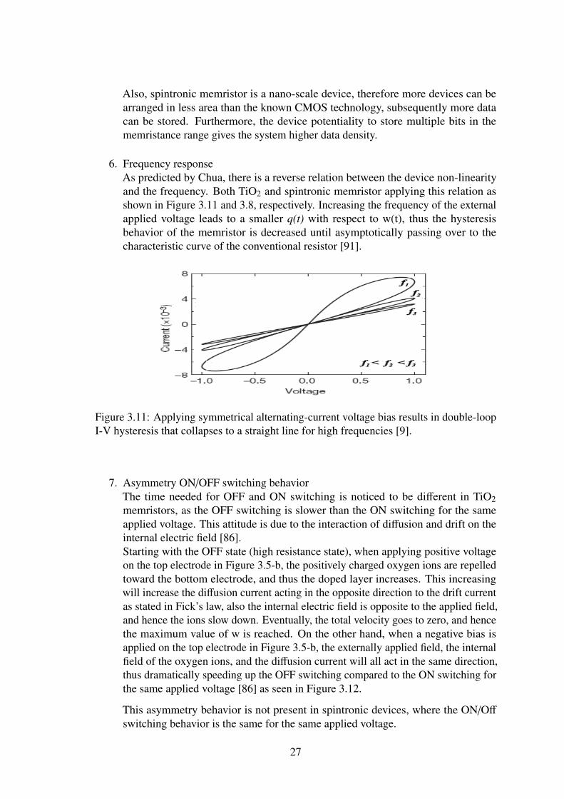
6. Frequency responseAs predicted by Chua, there is a reverse relation between the device non-linearityand the frequency. Both TiO2 and spintronic memristor applying this relation asshown in Figure 3.11 and 3.8, respectively. Increasing the frequency of the externalapplied voltage leads to a smaller q(t) with respect to w(t), thus the hysteresisbehavior of the memristor is decreased until asymptotically passing over to thecharacteristic curve of the conventional resistor [91].
Figure 3.11: Applying symmetrical alternating-current voltage bias results in double-loopI-V hysteresis that collapses to a straight line for high frequencies [9].
7. Asymmetry ON/OFF switching behaviorThe time needed for OFF and ON switching is noticed to be different in TiO2memristors, as the OFF switching is slower than the ON switching for the sameapplied voltage. This attitude is due to the interaction of diffusion and drift on theinternal electric field [86].Starting with the OFF state (high resistance state), when applying positive voltageon the top electrode in Figure 3.5-b, the positively charged oxygen ions are repelledtoward the bottom electrode, and thus the doped layer increases. This increasingwill increase the diffusion current acting in the opposite direction to the drift currentas stated in Fick’s law, also the internal electric field is opposite to the applied field,and hence the ions slow down. Eventually, the total velocity goes to zero, and hencethe maximum value of w is reached. On the other hand, when a negative bias isapplied on the top electrode in Figure 3.5-b, the externally applied field, the internalfield of the oxygen ions, and the diffusion current will all act in the same direction,thus dramatically speeding up the OFF switching compared to the ON switching forthe same applied voltage [86] as seen in Figure 3.12.
This asymmetry behavior is not present in spintronic devices, where the ON/Off
switching behavior is the same for the same applied voltage.
27
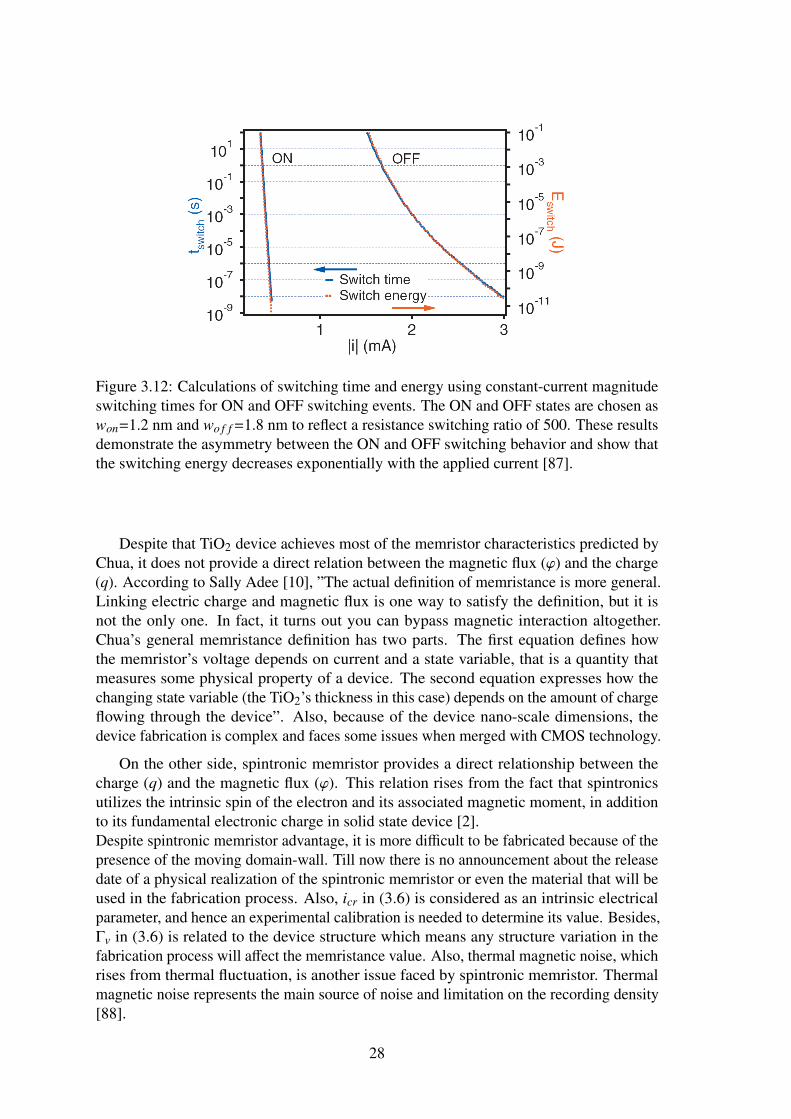
Figure 3.12: Calculations of switching time and energy using constant-current magnitudeswitching times for ON and OFF switching events. The ON and OFF states are chosen aswon=1.2 nm and wo f f =1.8 nm to reflect a resistance switching ratio of 500. These resultsdemonstrate the asymmetry between the ON and OFF switching behavior and show thatthe switching energy decreases exponentially with the applied current [87].
Despite that TiO2 device achieves most of the memristor characteristics predicted byChua, it does not provide a direct relation between the magnetic flux (ϕ) and the charge(q). According to Sally Adee [10], ”The actual definition of memristance is more general.Linking electric charge and magnetic flux is one way to satisfy the definition, but it isnot the only one. In fact, it turns out you can bypass magnetic interaction altogether.Chua’s general memristance definition has two parts. The first equation defines howthe memristor’s voltage depends on current and a state variable, that is a quantity thatmeasures some physical property of a device. The second equation expresses how thechanging state variable (the TiO2’s thickness in this case) depends on the amount of chargeflowing through the device”. Also, because of the device nano-scale dimensions, thedevice fabrication is complex and faces some issues when merged with CMOS technology.
On the other side, spintronic memristor provides a direct relationship between thecharge (q) and the magnetic flux (ϕ). This relation rises from the fact that spintronicsutilizes the intrinsic spin of the electron and its associated magnetic moment, in additionto its fundamental electronic charge in solid state device [2].Despite spintronic memristor advantage, it is more difficult to be fabricated because of thepresence of the moving domain-wall. Till now there is no announcement about the releasedate of a physical realization of the spintronic memristor or even the material that will beused in the fabrication process. Also, icr in (3.6) is considered as an intrinsic electricalparameter, and hence an experimental calibration is needed to determine its value. Besides,Γv in (3.6) is related to the device structure which means any structure variation in thefabrication process will affect the memristance value. Also, thermal magnetic noise, whichrises from thermal fluctuation, is another issue faced by spintronic memristor. Thermalmagnetic noise represents the main source of noise and limitation on the recording density[88].
28
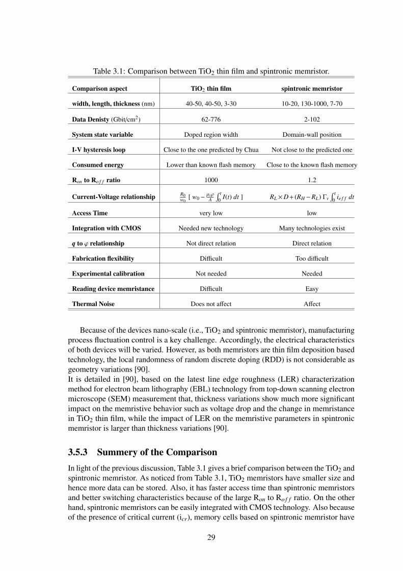
Table 3.1: Comparison between TiO2 thin film and spintronic memristor.
Comparison aspect TiO2 thin film spintronic memristor
width, length, thickness (nm) 40-50, 40-50, 3-30 10-20, 130-1000, 7-70
Data Denisty (Gbit/cm2) 62-776 2-102
System state variable Doped region width Domain-wall position
I-V hysteresis loop Close to the one predicted by Chua Not close to the predicted one
Consumed energy Lower than known flash memory Close to the known flash memory
Ron to Ro f f ratio 1000 1.2
Current-Voltage relationship R0w0
[ w0−µvρA
∫ t0 I(t) dt ] RL ×D + (RH −RL) Γv
∫ t0 ie f f dt
Access Time very low low
Integration with CMOS Needed new technology Many technologies exist
q to ϕ relationship Not direct relation Direct relation
Fabrication flexibility Difficult Too difficult
Experimental calibration Not needed Needed
Reading device memristance Difficult Easy
Thermal Noise Does not affect Affect
Because of the devices nano-scale (i.e., TiO2 and spintronic memristor), manufacturingprocess fluctuation control is a key challenge. Accordingly, the electrical characteristicsof both devices will be varied. However, as both memristors are thin film deposition basedtechnology, the local randomness of random discrete doping (RDD) is not considerable asgeometry variations [90].It is detailed in [90], based on the latest line edge roughness (LER) characterizationmethod for electron beam lithography (EBL) technology from top-down scanning electronmicroscope (SEM) measurement that, thickness variations show much more significantimpact on the memristive behavior such as voltage drop and the change in memristancein TiO2 thin film, while the impact of LER on the memristive parameters in spintronicmemristor is larger than thickness variations [90].
3.5.3 Summery of the ComparisonIn light of the previous discussion, Table 3.1 gives a brief comparison between the TiO2 andspintronic memristor. As noticed from Table 3.1, TiO2 memristors have smaller size andhence more data can be stored. Also, it has faster access time than spintronic memristorsand better switching characteristics because of the large Ron to Ro f f ratio. On the otherhand, spintronic memristors can be easily integrated with CMOS technology. Also becauseof the presence of critical current (icr), memory cells based on spintronic memristor have
29

better capabilities for reading the stored data without disturbing it. Therefore, the TiO2memristor is adopted through this thesis.
30
Chapter 4: Memristor Models andApplications
A lot of well evidenced circuit implementations based on TiO2 thin film memristorshave been published. For facilitating these applications and availability testing, differentmemristor models based on the real device published data were submitted [33, 92–97].These models can be classified into three main categories, mathematical models to facilitatethe device simulation within the Matlab simulation tools, Spice models, and Verilog-Amodels for device simulation with spice tools like Cadence Spectre tool.
The device applications cover both digital and analog domains [26, 28, 68, 98–104].Memristors used in digital circuit applications like non-volatile memory, signal processing,programmable logic, and control systems. Furthermore, memristors are potentially used forstateful logic implication, allowing a replacement for CMOS-based logic computation. Inthe analog regime, memristor based applications depend on the availability of continuouslyprogramming the device impedance. In this domain the device is used in applicationsconcerned with analog signal processing, learning circuits, programmable analog circuits,and neuromorphic circuits. Below, such models and applications are discussed, showingthe most promising ones.
4.1 Memristor Models
4.1.1 Mathematical Models
An analysis of the existing submitted memristor mathematical models were discussed in[92], where the predicted behavior of memristor using these models is compared to thereal device published properties. Three main models (i.e., Linear model, nonlinear model,and exponential model) were analyzed, compared, and converted into Matlab code in [92].Linear model is the basic model where the TiO2 thin film memristor is considered as alinear device. This model suffers from two main shortcomings, first the state variable(i.e., width of the doped region (w)) is not bounded by the device limitations (i.e., zeroand the device total length (D)). Besides, the model does not take into account the devicenon-linearity [92]. As a trial to deal with memristor non-linearity property, a nonlinearmodel was presented. It adds a non-linear window function F(x) (i.e., Strukov, Joglekar,or Biolek window function) to the state variable to bound it within the device boundaries.Biolek’s window function is added to the state variable. In this way, the reversed biaswill move back the state variable after reaching either boundary, and hence the windowfunction behaves differently in each voltage bias direction [92]. A more advanced model(exponential model) is also discussed. The exponential model fully fits the experimentallymeasured I-V characteristic curve of memristor, where at the OFF state the I-V curvebehaves like a P-N junction, and at the ON state the I-V curve follows a tunneling process[92]. These models (i.e., Linear, Non-linear, and Exponential model) are briefly comparedin Table 4.1.
31
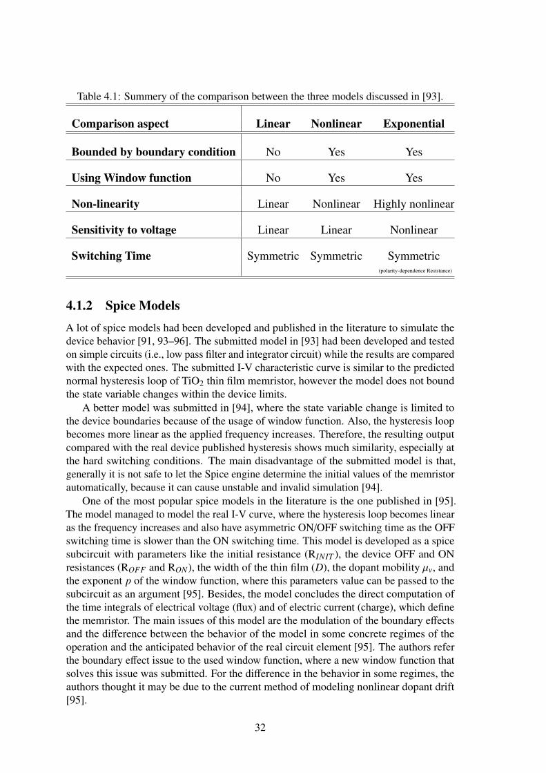
Table 4.1: Summery of the comparison between the three models discussed in [93].
Comparison aspect Linear Nonlinear Exponential
Bounded by boundary condition No Yes Yes
Using Window function No Yes Yes
Non-linearity Linear Nonlinear Highly nonlinear
Sensitivity to voltage Linear Linear Nonlinear
Switching Time Symmetric Symmetric Symmetric(polarity-dependence Resistance)
4.1.2 Spice ModelsA lot of spice models had been developed and published in the literature to simulate thedevice behavior [91, 93–96]. The submitted model in [93] had been developed and testedon simple circuits (i.e., low pass filter and integrator circuit) while the results are comparedwith the expected ones. The submitted I-V characteristic curve is similar to the predictednormal hysteresis loop of TiO2 thin film memristor, however the model does not boundthe state variable changes within the device limits.
A better model was submitted in [94], where the state variable change is limited tothe device boundaries because of the usage of window function. Also, the hysteresis loopbecomes more linear as the applied frequency increases. Therefore, the resulting outputcompared with the real device published hysteresis shows much similarity, especially atthe hard switching conditions. The main disadvantage of the submitted model is that,generally it is not safe to let the Spice engine determine the initial values of the memristorautomatically, because it can cause unstable and invalid simulation [94].
One of the most popular spice models in the literature is the one published in [95].The model managed to model the real I-V curve, where the hysteresis loop becomes linearas the frequency increases and also have asymmetric ON/OFF switching time as the OFFswitching time is slower than the ON switching time. This model is developed as a spicesubcircuit with parameters like the initial resistance (RINIT ), the device OFF and ONresistances (ROFF and RON), the width of the thin film (D), the dopant mobility µv, andthe exponent p of the window function, where this parameters value can be passed to thesubcircuit as an argument [95]. Besides, the model concludes the direct computation ofthe time integrals of electrical voltage (flux) and of electric current (charge), which definethe memristor. The main issues of this model are the modulation of the boundary effectsand the difference between the behavior of the model in some concrete regimes of theoperation and the anticipated behavior of the real circuit element [95]. The authors referthe boundary effect issue to the used window function, where a new window function thatsolves this issue was submitted. For the difference in the behavior in some regimes, theauthors thought it may be due to the current method of modeling nonlinear dopant drift[95].
32
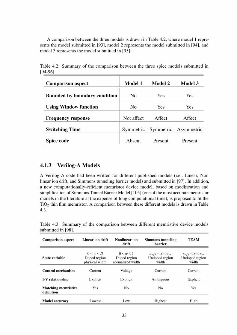
A comparison between the three models is drawn in Table 4.2, where model 1 repre-sents the model submitted in [93], model 2 represents the model submitted in [94], andmodel 3 represents the model submitted in [95].
Table 4.2: Summary of the comparison between the three spice models submitted in[94-96].
Comparison aspect Model 1 Model 2 Model 3
Bounded by boundary condition No Yes Yes
Using Window function No Yes Yes
Frequency response Not affect Affect Affect
Switching Time Symmetric Symmetric Asymmetric
Spice code Absent Present Present
4.1.3 Verilog-A Models
A Verilog-A code had been written for different published models (i.e., Linear, Nonlinear ion drift, and Simmons tunneling barrier model) and submitted in [97]. In addition,a new computationally-efficient memristor device model, based on modification andsimplification of Simmons Tunnel Barrier Model [105] (one of the most accurate memristormodels in the literature at the expense of long computational time), is proposed to fit theTiO2 thin film memristor. A comparison between these different models is drawn in Table4.3.
Table 4.3: Summary of the comparison between different memristive device modelssubmitted in [98].
Comparison aspect Linear ion drift Nonlinear ion Simmons tunneling TEAMdrift barrier
0 ≤ w ≤ D 0 ≤ w ≤ 1 ao f f ≤ x ≤ aon xo f f ≤ x ≤ xonState variable Doped region Doped region Undoped region Undoped region
physical width normalized width width width
Control mechanism Current Voltage Current Current
I-V relationship Explicit Explicit Ambiguous Explicit
Matching memristive Yes No No Yesdefinition
Model accuracy Lowest Low Highest High
33
Among all the proposed Verilog-A models in [97], this work will basically adoptThreshold Adaptive Memristor Model (TEAM model) in all of the following simulationsdue to the following reasons:
1. Model simplicity, generality and flexibilityTEAM model adopts simple and easy-to-understand equations to model the mem-ristor device and exhibit some fitting parameters. These fitting parameters make iteasier to expand the model to handle different material characteristics in order tomodel other memristor devices.
2. Computationally-efficient, and Sufficiently-accurate modelTEAM model is one of the fastest memristor device models in the literature [97].Simmons tunnel barrier is the best known accurate physical model of TiO2 memris-tive devices [86, 97]. However, this high accuracy of the Simmons model makes themodel complex and difficult to manipulate. TEAM model is based on the simplifica-tion of the Simmons model to provide high-accuracy and short computational time.The average error of the TEAM model compared to the Simmons model is 0.2%[97].
3. Model Suitability for circuit designSince the TEAM model is implemented in Verilog-A hardware description language,it is suitable to be integrated in Spice simulations.
The selection of the TEAM model to simulate the memristor behavior is based onconducting a comprehensive test on different memristor models. The test results provedthe previous advantages of the TEAM model over other models proposed in [97]. Anotherimportant concern of the model is the window function utilization. As discussed earlier,the window function is used to fit the boundary conditions and due to the significantnonlinearity variations in w, the used window affects the performance of the model.Therefore, a comprehensive test on different proposed window functions in [97] and itseffect on the model performance has been conducted to select the proper window functionwith respect to the chosen model. TEAM window shows better performance, betternonlinear dopant drift at device boundaries, and better nonlinear I-V characteristics whenintegrated with the TEAM model as compared to other literature window functions used in[97]. Accordingly, the TEAM window is selected to be adopted with the selected TEAMmodel for all the after-mentioned simulations.
4.2 Memristor ApplicationsAs memristor-based technology provides much better scalability and overall lower powerconsumption, many memristor-based applications were submitted in the literature like,
1. Neuromorphic circuitsOne of the most important and exciting applications is neuromorphic circuits. Neuro-morphic circuits are meant to emulate the human or animal brain. In neuromorphiccircuits, memristors are used as synapses which connect neurons to each other andstore information. As discussed in Chapter 3, the nano size of TiO2 memristor is
34
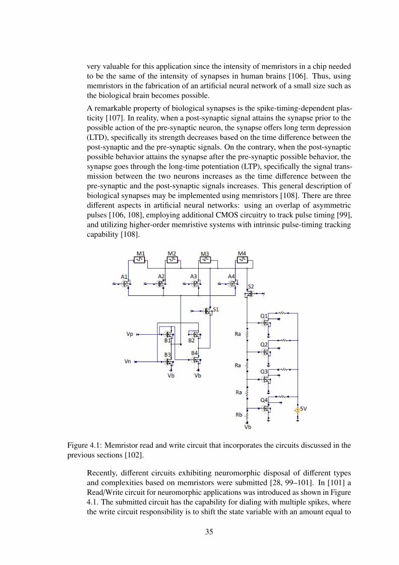
very valuable for this application since the intensity of memristors in a chip neededto be the same of the intensity of synapses in human brains [106]. Thus, usingmemristors in the fabrication of an artificial neural network of a small size such asthe biological brain becomes possible.
A remarkable property of biological synapses is the spike-timing-dependent plas-ticity [107]. In reality, when a post-synaptic signal attains the synapse prior to thepossible action of the pre-synaptic neuron, the synapse offers long term depression(LTD), specifically its strength decreases based on the time difference between thepost-synaptic and the pre-synaptic signals. On the contrary, when the post-synapticpossible behavior attains the synapse after the pre-synaptic possible behavior, thesynapse goes through the long-time potentiation (LTP), specifically the signal trans-mission between the two neurons increases as the time difference between thepre-synaptic and the post-synaptic signals increases. This general description ofbiological synapses may be implemented using memristors [108]. There are threedifferent aspects in artificial neural networks: using an overlap of asymmetricpulses [106, 108], employing additional CMOS circuitry to track pulse timing [99],and utilizing higher-order memristive systems with intrinsic pulse-timing trackingcapability [108].
Figure 4.1: Memristor read and write circuit that incorporates the circuits discussed in theprevious sections [102].
Recently, different circuits exhibiting neuromorphic disposal of different typesand complexities based on memristors were submitted [28, 99–101]. In [101] aRead/Write circuit for neuromorphic applications was introduced as shown in Figure4.1. The submitted circuit has the capability for dialing with multiple spikes, wherethe write circuit responsibility is to shift the state variable with an amount equal to
35
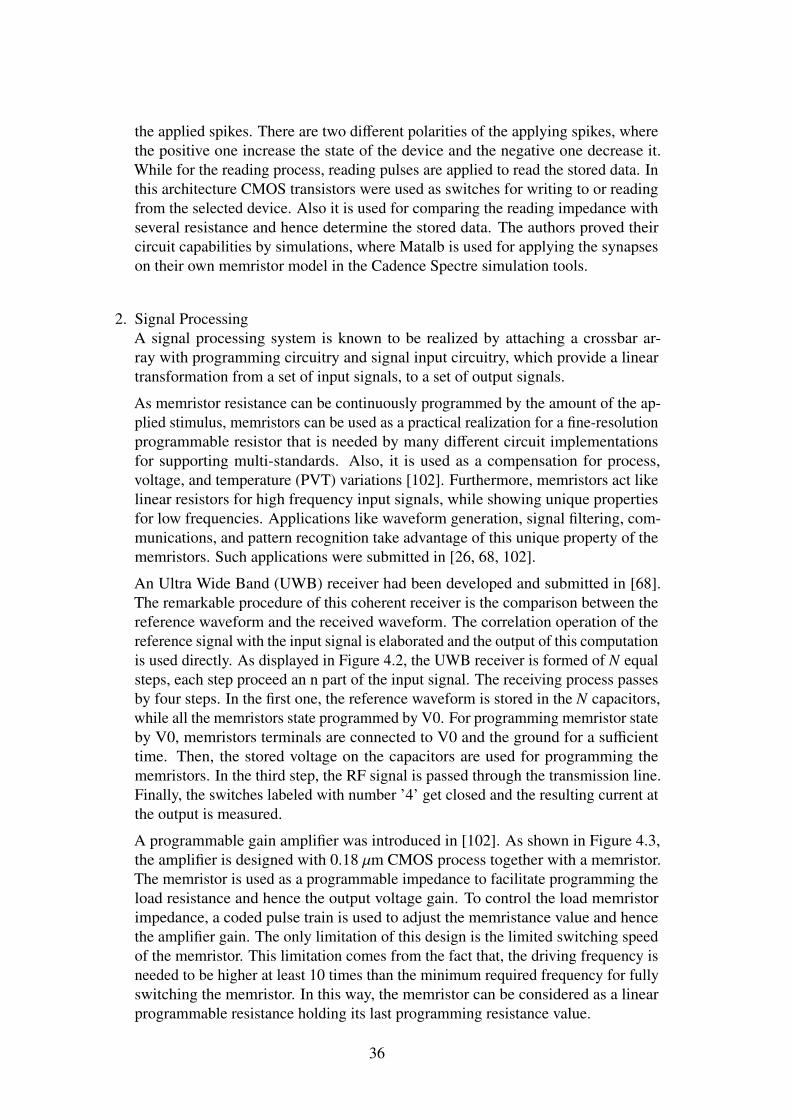
the applied spikes. There are two different polarities of the applying spikes, wherethe positive one increase the state of the device and the negative one decrease it.While for the reading process, reading pulses are applied to read the stored data. Inthis architecture CMOS transistors were used as switches for writing to or readingfrom the selected device. Also it is used for comparing the reading impedance withseveral resistance and hence determine the stored data. The authors proved theircircuit capabilities by simulations, where Matalb is used for applying the synapseson their own memristor model in the Cadence Spectre simulation tools.
2. Signal ProcessingA signal processing system is known to be realized by attaching a crossbar ar-ray with programming circuitry and signal input circuitry, which provide a lineartransformation from a set of input signals, to a set of output signals.
As memristor resistance can be continuously programmed by the amount of the ap-plied stimulus, memristors can be used as a practical realization for a fine-resolutionprogrammable resistor that is needed by many different circuit implementationsfor supporting multi-standards. Also, it is used as a compensation for process,voltage, and temperature (PVT) variations [102]. Furthermore, memristors act likelinear resistors for high frequency input signals, while showing unique propertiesfor low frequencies. Applications like waveform generation, signal filtering, com-munications, and pattern recognition take advantage of this unique property of thememristors. Such applications were submitted in [26, 68, 102].
An Ultra Wide Band (UWB) receiver had been developed and submitted in [68].The remarkable procedure of this coherent receiver is the comparison between thereference waveform and the received waveform. The correlation operation of thereference signal with the input signal is elaborated and the output of this computationis used directly. As displayed in Figure 4.2, the UWB receiver is formed of N equalsteps, each step proceed an n part of the input signal. The receiving process passesby four steps. In the first one, the reference waveform is stored in the N capacitors,while all the memristors state programmed by V0. For programming memristor stateby V0, memristors terminals are connected to V0 and the ground for a sufficienttime. Then, the stored voltage on the capacitors are used for programming thememristors. In the third step, the RF signal is passed through the transmission line.Finally, the switches labeled with number ’4’ get closed and the resulting current atthe output is measured.
A programmable gain amplifier was introduced in [102]. As shown in Figure 4.3,the amplifier is designed with 0.18 µm CMOS process together with a memristor.The memristor is used as a programmable impedance to facilitate programming theload resistance and hence the output voltage gain. To control the load memristorimpedance, a coded pulse train is used to adjust the memristance value and hencethe amplifier gain. The only limitation of this design is the limited switching speedof the memristor. This limitation comes from the fact that, the driving frequency isneeded to be higher at least 10 times than the minimum required frequency for fullyswitching the memristor. In this way, the memristor can be considered as a linearprogrammable resistance holding its last programming resistance value.
36
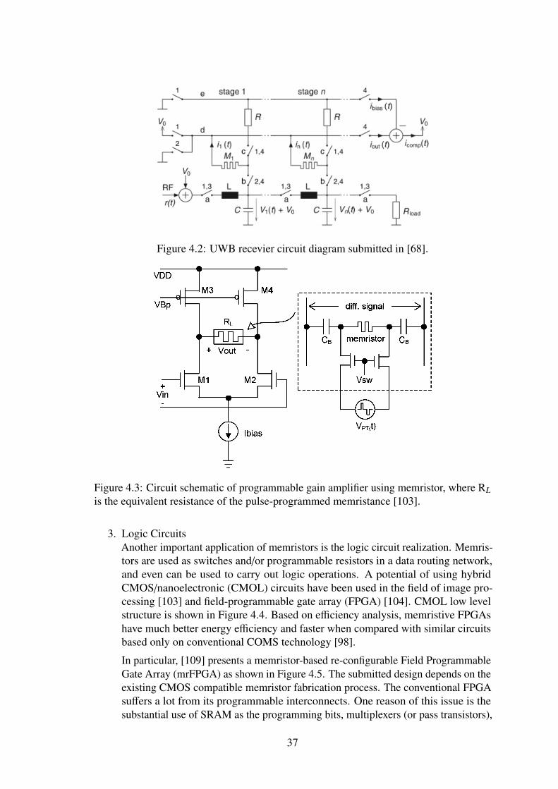
Figure 4.2: UWB recevier circuit diagram submitted in [68].
Figure 4.3: Circuit schematic of programmable gain amplifier using memristor, where RLis the equivalent resistance of the pulse-programmed memristance [103].
3. Logic CircuitsAnother important application of memristors is the logic circuit realization. Memris-tors are used as switches and/or programmable resistors in a data routing network,and even can be used to carry out logic operations. A potential of using hybridCMOS/nanoelectronic (CMOL) circuits have been used in the field of image pro-cessing [103] and field-programmable gate array (FPGA) [104]. CMOL low levelstructure is shown in Figure 4.4. Based on efficiency analysis, memristive FPGAshave much better energy efficiency and faster when compared with similar circuitsbased only on conventional COMS technology [98].
In particular, [109] presents a memristor-based re-configurable Field ProgrammableGate Array (mrFPGA) as shown in Figure 4.5. The submitted design depends on theexisting CMOS compatible memristor fabrication process. The conventional FPGAsuffers a lot from its programmable interconnects. One reason of this issue is thesubstantial use of SRAM as the programming bits, multiplexers (or pass transistors),
37
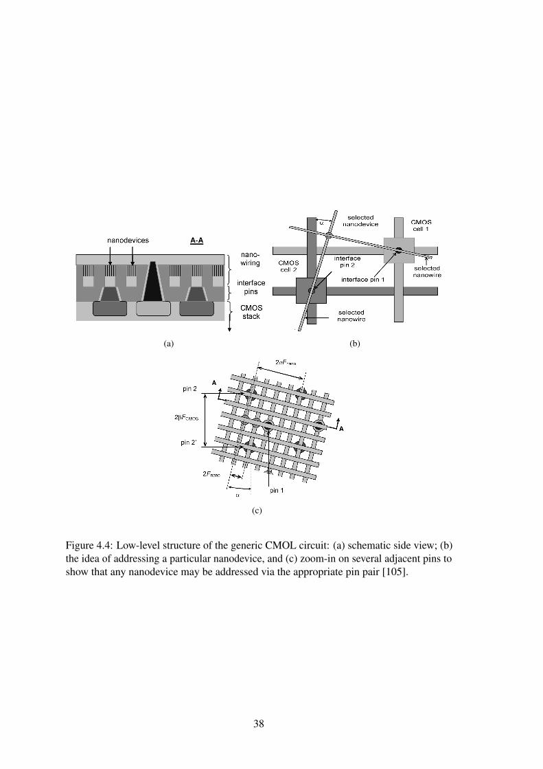
(a) (b)
(c)
Figure 4.4: Low-level structure of the generic CMOL circuit: (a) schematic side view; (b)the idea of addressing a particular nanodevice, and (c) zoom-in on several adjacent pins toshow that any nanodevice may be addressed via the appropriate pin pair [105].
38
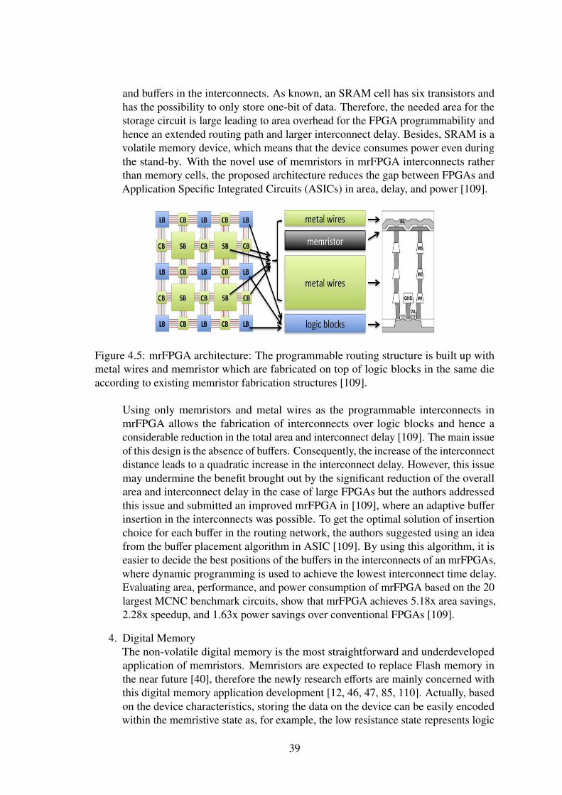
and buffers in the interconnects. As known, an SRAM cell has six transistors andhas the possibility to only store one-bit of data. Therefore, the needed area for thestorage circuit is large leading to area overhead for the FPGA programmability andhence an extended routing path and larger interconnect delay. Besides, SRAM is avolatile memory device, which means that the device consumes power even duringthe stand-by. With the novel use of memristors in mrFPGA interconnects ratherthan memory cells, the proposed architecture reduces the gap between FPGAs andApplication Specific Integrated Circuits (ASICs) in area, delay, and power [109].
Figure 4.5: mrFPGA architecture: The programmable routing structure is built up withmetal wires and memristor which are fabricated on top of logic blocks in the same dieaccording to existing memristor fabrication structures [109].
Using only memristors and metal wires as the programmable interconnects inmrFPGA allows the fabrication of interconnects over logic blocks and hence aconsiderable reduction in the total area and interconnect delay [109]. The main issueof this design is the absence of buffers. Consequently, the increase of the interconnectdistance leads to a quadratic increase in the interconnect delay. However, this issuemay undermine the benefit brought out by the significant reduction of the overallarea and interconnect delay in the case of large FPGAs but the authors addressedthis issue and submitted an improved mrFPGA in [109], where an adaptive bufferinsertion in the interconnects was possible. To get the optimal solution of insertionchoice for each buffer in the routing network, the authors suggested using an ideafrom the buffer placement algorithm in ASIC [109]. By using this algorithm, it iseasier to decide the best positions of the buffers in the interconnects of an mrFPGAs,where dynamic programming is used to achieve the lowest interconnect time delay.Evaluating area, performance, and power consumption of mrFPGA based on the 20largest MCNC benchmark circuits, show that mrFPGA achieves 5.18x area savings,2.28x speedup, and 1.63x power savings over conventional FPGAs [109].
4. Digital MemoryThe non-volatile digital memory is the most straightforward and underdevelopedapplication of memristors. Memristors are expected to replace Flash memory inthe near future [40], therefore the newly research efforts are mainly concerned withthis digital memory application development [12, 46, 47, 85, 110]. Actually, basedon the device characteristics, storing the data on the device can be easily encodedwithin the memristive state as, for example, the low resistance state represents logic
39
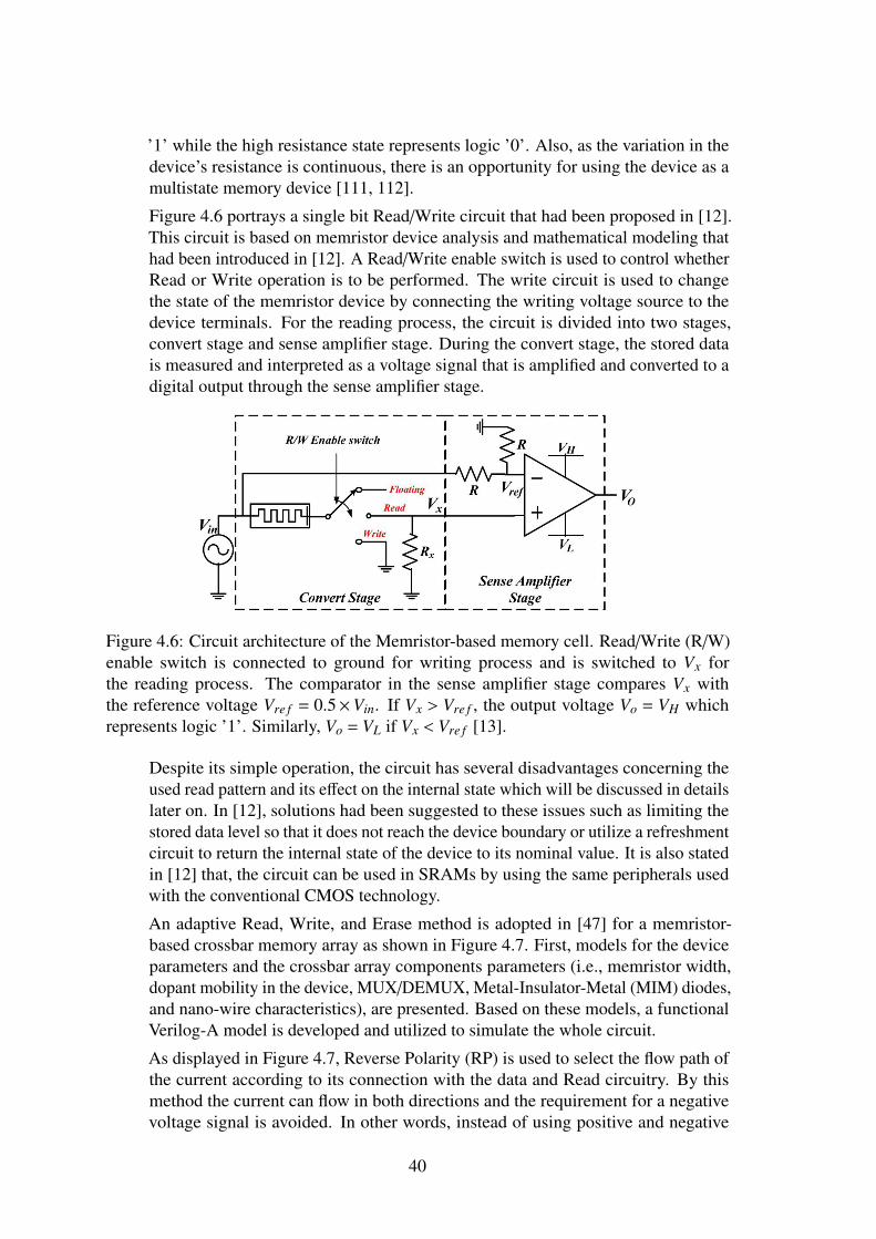
’1’ while the high resistance state represents logic ’0’. Also, as the variation in thedevice’s resistance is continuous, there is an opportunity for using the device as amultistate memory device [111, 112].
Figure 4.6 portrays a single bit Read/Write circuit that had been proposed in [12].This circuit is based on memristor device analysis and mathematical modeling thathad been introduced in [12]. A Read/Write enable switch is used to control whetherRead or Write operation is to be performed. The write circuit is used to changethe state of the memristor device by connecting the writing voltage source to thedevice terminals. For the reading process, the circuit is divided into two stages,convert stage and sense amplifier stage. During the convert stage, the stored datais measured and interpreted as a voltage signal that is amplified and converted to adigital output through the sense amplifier stage.
Figure 4.6: Circuit architecture of the Memristor-based memory cell. Read/Write (R/W)enable switch is connected to ground for writing process and is switched to Vx forthe reading process. The comparator in the sense amplifier stage compares Vx withthe reference voltage Vre f = 0.5×Vin. If Vx > Vre f , the output voltage Vo = VH whichrepresents logic ’1’. Similarly, Vo = VL if Vx < Vre f [13].
Despite its simple operation, the circuit has several disadvantages concerning theused read pattern and its effect on the internal state which will be discussed in detailslater on. In [12], solutions had been suggested to these issues such as limiting thestored data level so that it does not reach the device boundary or utilize a refreshmentcircuit to return the internal state of the device to its nominal value. It is also statedin [12] that, the circuit can be used in SRAMs by using the same peripherals usedwith the conventional CMOS technology.
An adaptive Read, Write, and Erase method is adopted in [47] for a memristor-based crossbar memory array as shown in Figure 4.7. First, models for the deviceparameters and the crossbar array components parameters (i.e., memristor width,dopant mobility in the device, MUX/DEMUX, Metal-Insulator-Metal (MIM) diodes,and nano-wire characteristics), are presented. Based on these models, a functionalVerilog-A model is developed and utilized to simulate the whole circuit.
As displayed in Figure 4.7, Reverse Polarity (RP) is used to select the flow path ofthe current according to its connection with the data and Read circuitry. By thismethod the current can flow in both directions and the requirement for a negativevoltage signal is avoided. In other words, instead of using positive and negative
40
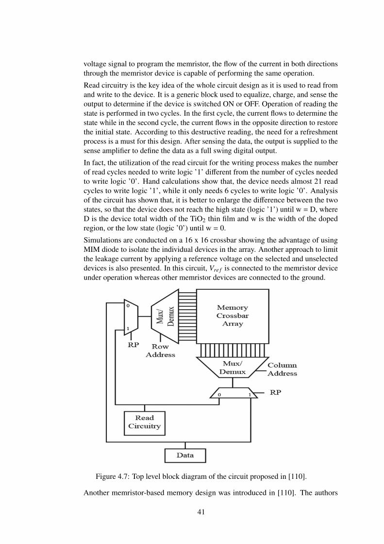
voltage signal to program the memristor, the flow of the current in both directionsthrough the memristor device is capable of performing the same operation.
Read circuitry is the key idea of the whole circuit design as it is used to read fromand write to the device. It is a generic block used to equalize, charge, and sense theoutput to determine if the device is switched ON or OFF. Operation of reading thestate is performed in two cycles. In the first cycle, the current flows to determine thestate while in the second cycle, the current flows in the opposite direction to restorethe initial state. According to this destructive reading, the need for a refreshmentprocess is a must for this design. After sensing the data, the output is supplied to thesense amplifier to define the data as a full swing digital output.
In fact, the utilization of the read circuit for the writing process makes the numberof read cycles needed to write logic ’1’ different from the number of cycles neededto write logic ’0’. Hand calculations show that, the device needs almost 21 readcycles to write logic ’1’, while it only needs 6 cycles to write logic ’0’. Analysisof the circuit has shown that, it is better to enlarge the difference between the twostates, so that the device does not reach the high state (logic ’1’) until w = D, whereD is the device total width of the TiO2 thin film and w is the width of the dopedregion, or the low state (logic ’0’) until w = 0.
Simulations are conducted on a 16 x 16 crossbar showing the advantage of usingMIM diode to isolate the individual devices in the array. Another approach to limitthe leakage current by applying a reference voltage on the selected and unselecteddevices is also presented. In this circuit, Vre f is connected to the memristor deviceunder operation whereas other memristor devices are connected to the ground.
Figure 4.7: Top level block diagram of the circuit proposed in [110].
Another memristor-based memory design was introduced in [110]. The authors
41

introduced an observation about the memristor’s asymmetric energy consumptionby detailed analysis of the transient power consumption. Based on this perception,a dual element memristor based memory is introduced. Memory cell consists oftwo memristors where one is used to store the data as it is written and the otheris used to store the complementary data. Each memristor is individually written.While in the reading process, both memristance values are compared to read thestored data. Based on energy optimization and partial programming, authors in[110] presented four different optimization schemes where one scheme was claimedto save the energy by 80%. Also, [110] introduced different optimization schemesfor speed and resistance distinguishability to apply on the dual element circuit tomake it suitable for different applications as each one of these schemes provided asolution to one of the memristor design constraints (i.e., resistance distinguishabilitybetween the high resistance and low resistance, reading or writing latency, voltageusage for reading or writing memristors, and energy consumption). Each one ofthose schemes has its advantages and drawbacks which make it suitable for someapplications and not suitable for others.
42
Chapter 5: Memory design insights andnew proposed circuitsIn this chapter Memristor-based Memory Design Insights are discussed. Based on thisinsights, three Read/Write memristor-based memory cells are proposed.
5.1 Memristor-based Memory Design Insights
5.1.1 Design ConsiderationsIn light of the device analysis introduced in Chapter 3, the design considerations of usinga memristor in the realization of a memory cell are summarized as follows:
1. Nano-scale constraintsBecause of the device nano-scale, the oxygen atoms are free to move inside thedevice with a sensible rate, where the device resistance is changing according tothis movement. On the other hand, manufacturing process fluctuations controlis a key challenge. It is detailed in [90], based on the latest line edge roughness(LER) characterization method for electron beam lithography (EBL) technologyfrom top-down scanning electron microscope (SEM) measurement that, thicknessvariations show significant impact on the memristive behaviors such as voltagedrop and the change in the memristance value. Also, integration of the device withCMOS technology may face some issues because of the differences in the devicesscales.
2. Bipolar deviceAs the device state depends on the direction of the passing current, hence goodattention should be given to the current direction passing through the device duringthe reading process, the writing process, or the idle state. Otherwise, a wrong datamay be written or erased during such processes.
3. Device non-volatilityMemristors store the data as a resistivity. This resistance depends on the oxygenatoms movement, which is caused by the applied stimulus. Thus, if this stimulus isswitched off, the oxygen atoms keep its last position. The non-volatile advantage ofthe device, which makes the device a good candidate for memory applications, maybe lost during the memory cell design. This loss comes from designing a memorycircuits based on volatile elements (i.e., Latches) beside the memristor.
4. Consumed energy and timeThe main important constraints in any electronic system design are the energyconsumption (E) and the response time (t). The consumed energy can be computedas in [86]:
E =
∫i× v(w) dw
w(5.1)
43
From (3.2) and (5.1), it is obvious that the consumed energy (E) decreases exponen-tially as the current passing through the device (i) increases. Accordingly, the heatis decreased. Also, the time required to switch a device between two states (4t) canbe computed as in [86]:
4 t =
∫dww
(5.2)
which indicates, due to (3.1), (3.2), and (5.2), that the time decreases exponentiallyas the applied current increases. Figure 3.12 shows the relation between the appliedcurrent (i), the consumed energy (E), and the switching time (t).
Therefore, writing logic ’1’ may need more voltage than writing logic ’0’. This isbecause the nonlinear memristor I-V characteristics as illustrated in Figure 3.6.
5. Memristance swithingMigration between doped region low resistance and un-doped region high resistancerepresents the system resistivity, named system memristance as in (3.6). Accordingly,memristance is not discrete, instead it is continuous over the time.
It is important to mention that, the electrodes nano size results in a series resistancein the range of kOhms, while the device ON resistance is in the range of Ohms.Therefore, the series resistance is larger than the device ON resistance and hence,the device (i.e., switching material TiO2−x) consumed more current to reset [113].This consumed current results in increasing the power consumption.
6. High density memories designBecause of the device nano-scale, memristor has better scalability, which meansmore devices can be arranged in the same area that is used for the known CMOStechnology, and hence more data is stored. Besides, device memristance continuitymakes it possible to store multiple bits instead of one bit as in conventional memorydevices.
7. Frequency responseThere is a reverse relation between the TiO2 memristor non-linearity and the fre-quency as shown in Figure 3.11.
Therefore, using a higher frequency input source degenerates the device non-linearity, and hence make the system design easier.
8. Asymmetric ON/OFF switching behaviorThe time needed for OFF and ON switching are noticed to be different, as the OFFswitching time is slower than the ON switching time for the same applied voltage asshown in Figure 3.12. This attitude is due to the interaction of diffusion and drift onthe internal electric field [114].
9. Stimulus dependenceMemristance value depends on the total charge injection regardless the source shape,this fact comes from the device unique signal processing criteria. The only thingthat matters is the net applied injection and the period of the applied stimuli.
44
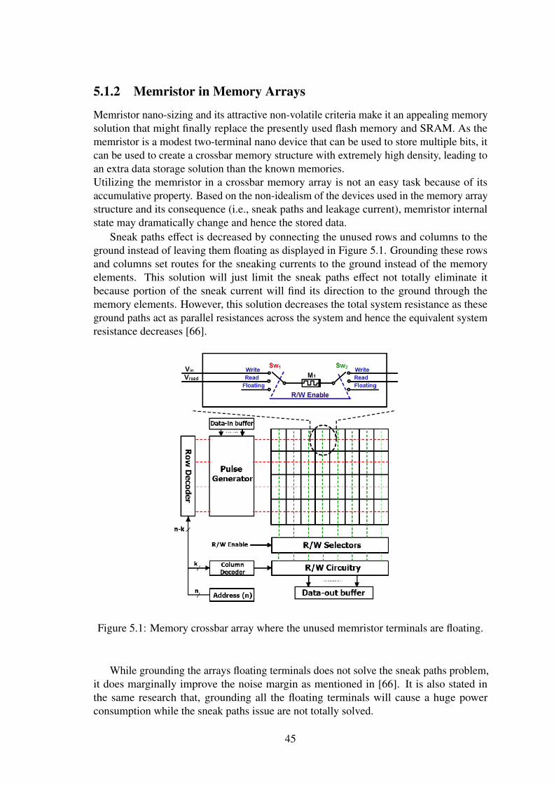
5.1.2 Memristor in Memory Arrays
Memristor nano-sizing and its attractive non-volatile criteria make it an appealing memorysolution that might finally replace the presently used flash memory and SRAM. As thememristor is a modest two-terminal nano device that can be used to store multiple bits, itcan be used to create a crossbar memory structure with extremely high density, leading toan extra data storage solution than the known memories.Utilizing the memristor in a crossbar memory array is not an easy task because of itsaccumulative property. Based on the non-idealism of the devices used in the memory arraystructure and its consequence (i.e., sneak paths and leakage current), memristor internalstate may dramatically change and hence the stored data.
Sneak paths effect is decreased by connecting the unused rows and columns to theground instead of leaving them floating as displayed in Figure 5.1. Grounding these rowsand columns set routes for the sneaking currents to the ground instead of the memoryelements. This solution will just limit the sneak paths effect not totally eliminate itbecause portion of the sneak current will find its direction to the ground through thememory elements. However, this solution decreases the total system resistance as theseground paths act as parallel resistances across the system and hence the equivalent systemresistance decreases [66].
Figure 5.1: Memory crossbar array where the unused memristor terminals are floating.
While grounding the arrays floating terminals does not solve the sneak paths problem,it does marginally improve the noise margin as mentioned in [66]. It is also stated inthe same research that, grounding all the floating terminals will cause a huge powerconsumption while the sneak paths issue are not totally solved.
45
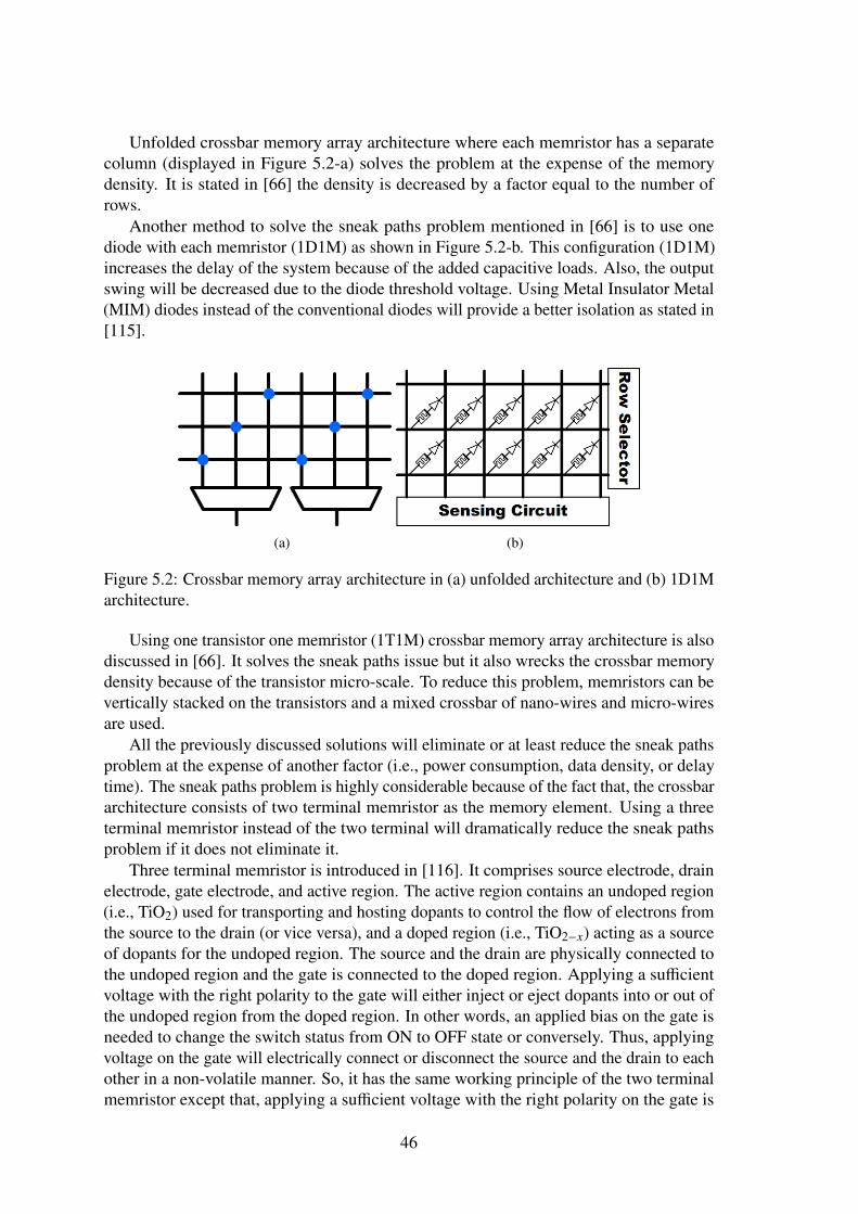
Unfolded crossbar memory array architecture where each memristor has a separatecolumn (displayed in Figure 5.2-a) solves the problem at the expense of the memorydensity. It is stated in [66] the density is decreased by a factor equal to the number ofrows.
Another method to solve the sneak paths problem mentioned in [66] is to use onediode with each memristor (1D1M) as shown in Figure 5.2-b. This configuration (1D1M)increases the delay of the system because of the added capacitive loads. Also, the outputswing will be decreased due to the diode threshold voltage. Using Metal Insulator Metal(MIM) diodes instead of the conventional diodes will provide a better isolation as stated in[115].
(a) (b)
Figure 5.2: Crossbar memory array architecture in (a) unfolded architecture and (b) 1D1Marchitecture.
Using one transistor one memristor (1T1M) crossbar memory array architecture is alsodiscussed in [66]. It solves the sneak paths issue but it also wrecks the crossbar memorydensity because of the transistor micro-scale. To reduce this problem, memristors can bevertically stacked on the transistors and a mixed crossbar of nano-wires and micro-wiresare used.
All the previously discussed solutions will eliminate or at least reduce the sneak pathsproblem at the expense of another factor (i.e., power consumption, data density, or delaytime). The sneak paths problem is highly considerable because of the fact that, the crossbararchitecture consists of two terminal memristor as the memory element. Using a threeterminal memristor instead of the two terminal will dramatically reduce the sneak pathsproblem if it does not eliminate it.
Three terminal memristor is introduced in [116]. It comprises source electrode, drainelectrode, gate electrode, and active region. The active region contains an undoped region(i.e., TiO2) used for transporting and hosting dopants to control the flow of electrons fromthe source to the drain (or vice versa), and a doped region (i.e., TiO2−x) acting as a sourceof dopants for the undoped region. The source and the drain are physically connected tothe undoped region and the gate is connected to the doped region. Applying a sufficientvoltage with the right polarity to the gate will either inject or eject dopants into or out ofthe undoped region from the doped region. In other words, an applied bias on the gate isneeded to change the switch status from ON to OFF state or conversely. Thus, applyingvoltage on the gate will electrically connect or disconnect the source and the drain to eachother in a non-volatile manner. So, it has the same working principle of the two terminalmemristor except that, applying a sufficient voltage with the right polarity on the gate is
46
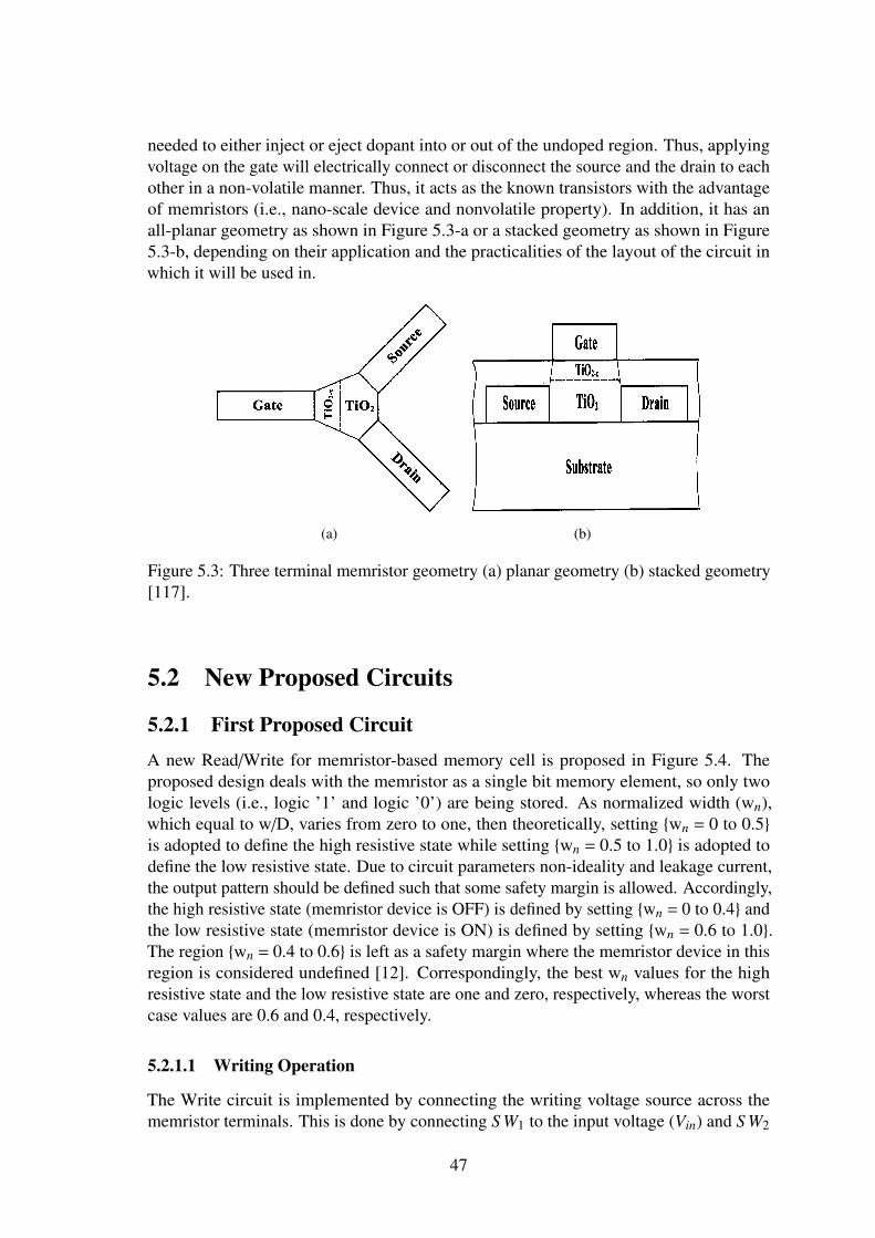
needed to either inject or eject dopant into or out of the undoped region. Thus, applyingvoltage on the gate will electrically connect or disconnect the source and the drain to eachother in a non-volatile manner. Thus, it acts as the known transistors with the advantageof memristors (i.e., nano-scale device and nonvolatile property). In addition, it has anall-planar geometry as shown in Figure 5.3-a or a stacked geometry as shown in Figure5.3-b, depending on their application and the practicalities of the layout of the circuit inwhich it will be used in.
(a) (b)
Figure 5.3: Three terminal memristor geometry (a) planar geometry (b) stacked geometry[117].
5.2 New Proposed Circuits
5.2.1 First Proposed CircuitA new Read/Write for memristor-based memory cell is proposed in Figure 5.4. Theproposed design deals with the memristor as a single bit memory element, so only twologic levels (i.e., logic ’1’ and logic ’0’) are being stored. As normalized width (wn),which equal to w/D, varies from zero to one, then theoretically, setting wn = 0 to 0.5is adopted to define the high resistive state while setting wn = 0.5 to 1.0 is adopted todefine the low resistive state. Due to circuit parameters non-ideality and leakage current,the output pattern should be defined such that some safety margin is allowed. Accordingly,the high resistive state (memristor device is OFF) is defined by setting wn = 0 to 0.4 andthe low resistive state (memristor device is ON) is defined by setting wn = 0.6 to 1.0.The region wn = 0.4 to 0.6 is left as a safety margin where the memristor device in thisregion is considered undefined [12]. Correspondingly, the best wn values for the highresistive state and the low resistive state are one and zero, respectively, whereas the worstcase values are 0.6 and 0.4, respectively.
5.2.1.1 Writing Operation
The Write circuit is implemented by connecting the writing voltage source across thememristor terminals. This is done by connecting S W1 to the input voltage (Vin) and S W2
47
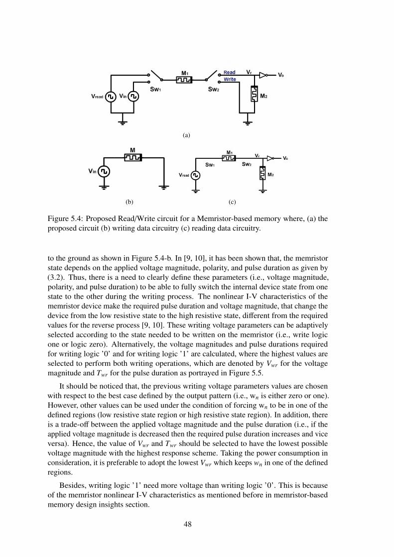
(a)
(b) (c)
Figure 5.4: Proposed Read/Write circuit for a Memristor-based memory where, (a) theproposed circuit (b) writing data circuitry (c) reading data circuitry.
to the ground as shown in Figure 5.4-b. In [9, 10], it has been shown that, the memristorstate depends on the applied voltage magnitude, polarity, and pulse duration as given by(3.2). Thus, there is a need to clearly define these parameters (i.e., voltage magnitude,polarity, and pulse duration) to be able to fully switch the internal device state from onestate to the other during the writing process. The nonlinear I-V characteristics of thememristor device make the required pulse duration and voltage magnitude, that change thedevice from the low resistive state to the high resistive state, different from the requiredvalues for the reverse process [9, 10]. These writing voltage parameters can be adaptivelyselected according to the state needed to be written on the memristor (i.e., write logicone or logic zero). Alternatively, the voltage magnitudes and pulse durations requiredfor writing logic ’0’ and for writing logic ’1’ are calculated, where the highest values areselected to perform both writing operations, which are denoted by Vwr for the voltagemagnitude and Twr for the pulse duration as portrayed in Figure 5.5.
It should be noticed that, the previous writing voltage parameters values are chosenwith respect to the best case defined by the output pattern (i.e., wn is either zero or one).However, other values can be used under the condition of forcing wn to be in one of thedefined regions (low resistive state region or high resistive state region). In addition, thereis a trade-off between the applied voltage magnitude and the pulse duration (i.e., if theapplied voltage magnitude is decreased then the required pulse duration increases and viceversa). Hence, the value of Vwr and Twr should be selected to have the lowest possiblevoltage magnitude with the highest response scheme. Taking the power consumption inconsideration, it is preferable to adopt the lowest Vwr which keeps wn in one of the definedregions.
Besides, writing logic ’1’ need more voltage than writing logic ’0’. This is becauseof the memristor nonlinear I-V characteristics as mentioned before in memristor-basedmemory design insights section.
48
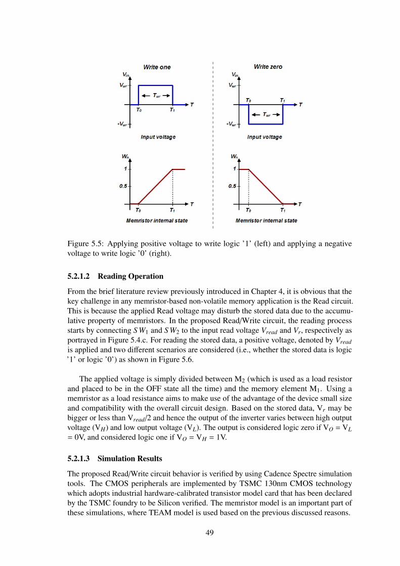
Figure 5.5: Applying positive voltage to write logic ’1’ (left) and applying a negativevoltage to write logic ’0’ (right).
5.2.1.2 Reading Operation
From the brief literature review previously introduced in Chapter 4, it is obvious that thekey challenge in any memristor-based non-volatile memory application is the Read circuit.This is because the applied Read voltage may disturb the stored data due to the accumu-lative property of memristors. In the proposed Read/Write circuit, the reading processstarts by connecting S W1 and S W2 to the input read voltage Vread and Vr, respectively asportrayed in Figure 5.4.c. For reading the stored data, a positive voltage, denoted by Vreadis applied and two different scenarios are considered (i.e., whether the stored data is logic’1’ or logic ’0’) as shown in Figure 5.6.
The applied voltage is simply divided between M2 (which is used as a load resistorand placed to be in the OFF state all the time) and the memory element M1. Using amemristor as a load resistance aims to make use of the advantage of the device small sizeand compatibility with the overall circuit design. Based on the stored data, Vr may bebigger or less than Vread/2 and hence the output of the inverter varies between high outputvoltage (VH) and low output voltage (VL). The output is considered logic zero if VO = VL= 0V, and considered logic one if VO = VH = 1V.
5.2.1.3 Simulation Results
The proposed Read/Write circuit behavior is verified by using Cadence Spectre simulationtools. The CMOS peripherals are implemented by TSMC 130nm CMOS technologywhich adopts industrial hardware-calibrated transistor model card that has been declaredby the TSMC foundry to be Silicon verified. The memristor model is an important part ofthese simulations, where TEAM model is used based on the previous discussed reasons.
49
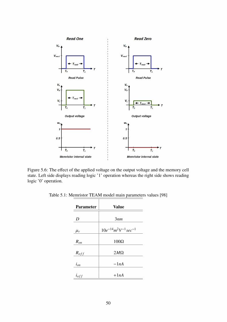
Figure 5.6: The effect of the applied voltage on the output voltage and the memory cellstate. Left side displays reading logic ’1’ operation whereas the right side shows readinglogic ’0’ operation.
Table 5.1: Memristor TEAM model main parameters values [98]
Parameter Value
D 3nm
µv 10e−14m2V−1sec−1
Ron 100Ω
Ro f f 2MΩ
ion −1nA
io f f +1nA
50
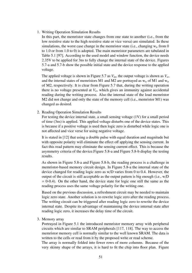
1. Writing Operation Simulation ResultsIn this part, the memristor state changes from one state to another (i.e., from thelow resistive state to the high resistive state or vice versa) are simulated. In thesesimulations, the worst case change in the memristor state (i.e., changing wn from 0to 1.0 or from 1.0 to 0) is adopted. The main memristor parameters are tabulated inTable 5.1 [97]. According to the used model and window function, the device needs2.35V to be applied for 3ns to fully change the internal state of the device. Figures5.7-a and 5.7-b show the possible initial state and the device response to the appliedvoltage.
The applied voltage is shown in Figure 5.7 as Vin, the output voltage is shown as Vo,and the internal states of memristors M1 and M2 are portrayed as wn of M1 and wnof M2, respectively. It is clear from Figure 5.7 that, during the writing operationthere is no voltage presented at Vo, which gives an immunity against accidentalreading during the writing process. Also the internal state of the load memristorM2 did not change and only the state of the memory cell (i.e., memristor M1) waschanged as desired.
2. Reading Operation Simulation ResultsFor testing the device internal state, a small sensing voltage (1V) for a small periodof time (3ns) is applied. This applied voltage disturbs one of the device states. Thisis because if a positive voltage is used then logic zero is disturbed while logic one isnot affected and vice verse for using negative voltage.
It is stated in [12] that using a double pulse with equal duration and magnitude butwith opposite polarity will eliminate the effect off applying the sensing current. Infact this read pattern may eliminate the sensing current effect. This is because theasymmetry criteria of the device.Figure 5.8-a and Figure 5.8-b display the testingresults.
As shown in Figure 5.8-a and Figure 5.8-b, the reading process is a challenge inmemristor-based memory circuit design. In Figure 5.8-a the internal state of thedevice changed for reading logic zero as w/D varies from 0 to 0.4. However, theoutput of the circuit is still acceptable as the output pattern is big enough (i.e., w/D= 0-0.4). On the other hand, the device state for logic one still the same as thereading process uses the same voltage polarity for the writing one.
Based on the previous discussion, a refreshment circuit may be needed to maintainlogic zero state. Another solution is to rewrite logic zero after the reading process.The writing circuit can be triggered after reading logic zero to rewrite the deviceinternal state. Despite its advantage of maintaining the device internal state afterreading logic zero, it increases the delay time of the circuit.
3. Memory arrayPortrayed in Figure 5.1 the introduced memristor memory array with peripheralcircuits which are similar to SRAM peripherals [117, 118]. The way to access thememristor memory cell is normally similar to the well known SRAM. The data iswritten to the cells or read from it by the proposed write or read scheme.The array is normally folded into fewer rows of more columns. Because of thevery skinny shape of the arrays, it is hard to fit the chip into floor plan. Figure
51
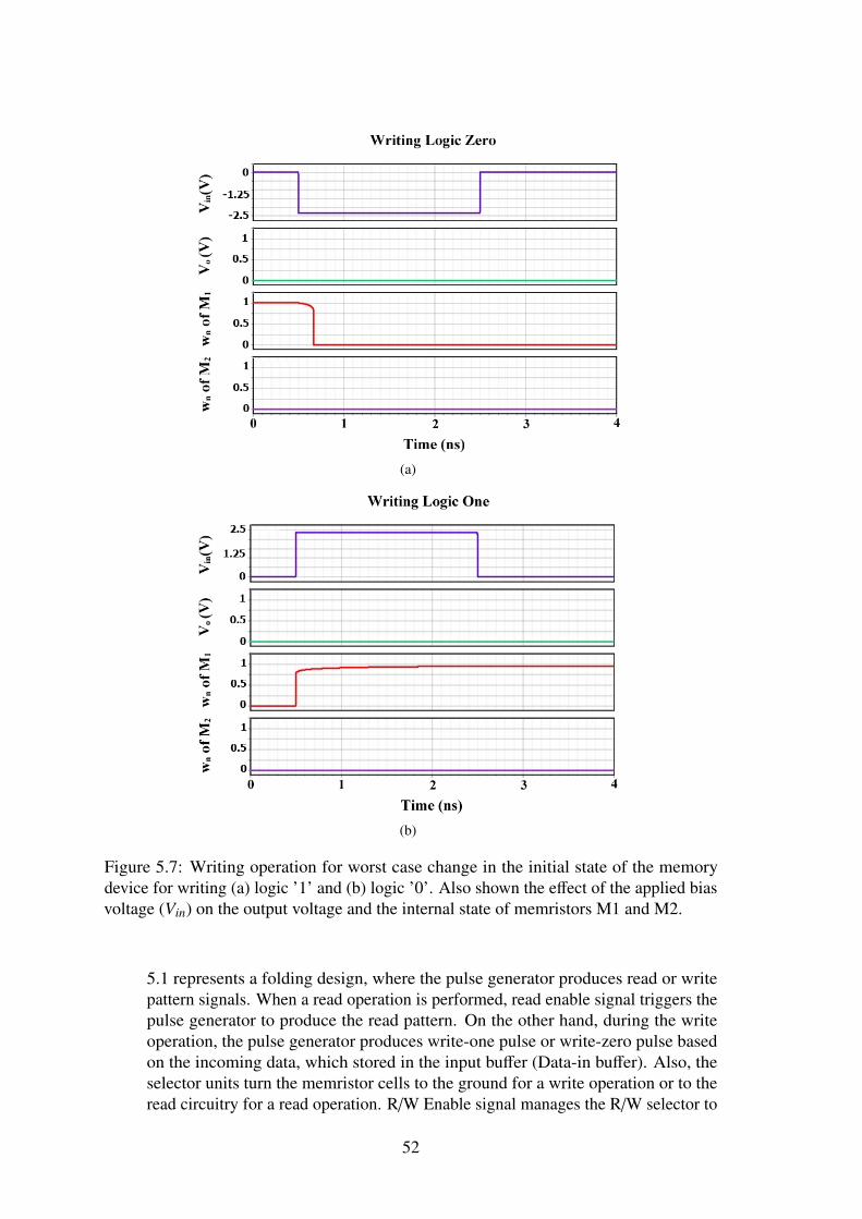
(a)
(b)
Figure 5.7: Writing operation for worst case change in the initial state of the memorydevice for writing (a) logic ’1’ and (b) logic ’0’. Also shown the effect of the applied biasvoltage (Vin) on the output voltage and the internal state of memristors M1 and M2.
5.1 represents a folding design, where the pulse generator produces read or writepattern signals. When a read operation is performed, read enable signal triggers thepulse generator to produce the read pattern. On the other hand, during the writeoperation, the pulse generator produces write-one pulse or write-zero pulse basedon the incoming data, which stored in the input buffer (Data-in buffer). Also, theselector units turn the memristor cells to the ground for a write operation or to theread circuitry for a read operation. R/W Enable signal manages the R/W selector to
52
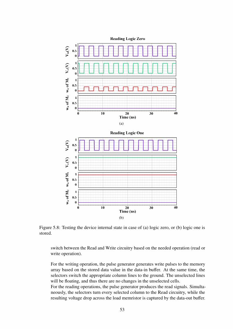
(a)
(b)
Figure 5.8: Testing the device internal state in case of (a) logic zero, or (b) logic one isstored.
switch between the Read and Write circuitry based on the needed operation (read orwrite operation).
For the writing operation, the pulse generator generates write pulses to the memoryarray based on the stored data value in the data-in buffer. At the same time, theselectors switch the appropriate column lines to the ground. The unselected lineswill be floating, and thus there are no changes in the unselected cells.For the reading operations, the pulse generator produces the read signals. Simulta-neously, the selectors turn every selected column to the Read circuitry, while theresulting voltage drop across the load memristor is captured by the data-out buffer.
53
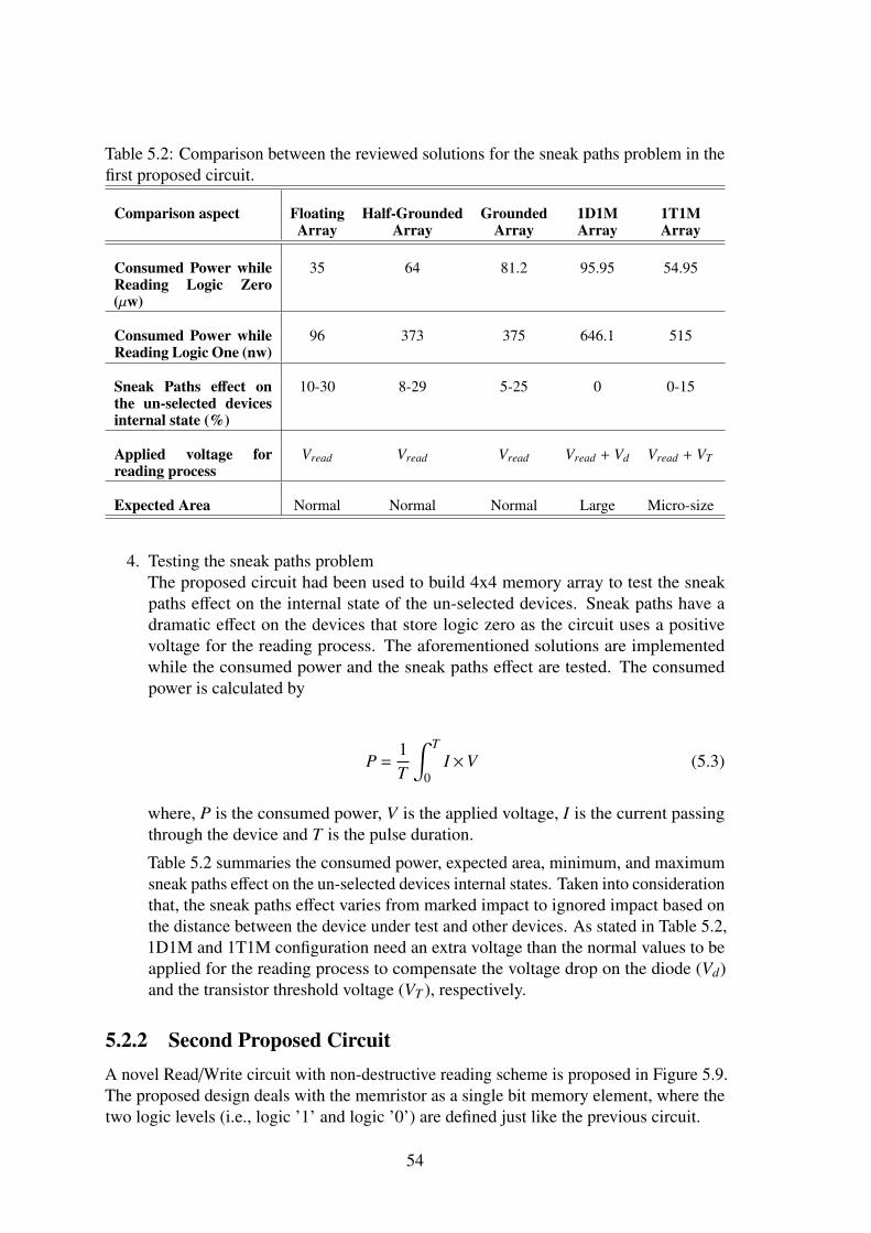
Table 5.2: Comparison between the reviewed solutions for the sneak paths problem in thefirst proposed circuit.
Comparison aspect Floating Half-Grounded Grounded 1D1M 1T1MArray Array Array Array Array
Consumed Power whileReading Logic Zero(µw)
35 64 81.2 95.95 54.95
Consumed Power whileReading Logic One (nw)
96 373 375 646.1 515
Sneak Paths effect onthe un-selected devicesinternal state (%)
10-30 8-29 5-25 0 0-15
Applied voltage forreading process
Vread Vread Vread Vread + Vd Vread + VT
Expected Area Normal Normal Normal Large Micro-size
4. Testing the sneak paths problemThe proposed circuit had been used to build 4x4 memory array to test the sneakpaths effect on the internal state of the un-selected devices. Sneak paths have adramatic effect on the devices that store logic zero as the circuit uses a positivevoltage for the reading process. The aforementioned solutions are implementedwhile the consumed power and the sneak paths effect are tested. The consumedpower is calculated by
P =1T
∫ T
0I×V (5.3)
where, P is the consumed power, V is the applied voltage, I is the current passingthrough the device and T is the pulse duration.
Table 5.2 summaries the consumed power, expected area, minimum, and maximumsneak paths effect on the un-selected devices internal states. Taken into considerationthat, the sneak paths effect varies from marked impact to ignored impact based onthe distance between the device under test and other devices. As stated in Table 5.2,1D1M and 1T1M configuration need an extra voltage than the normal values to beapplied for the reading process to compensate the voltage drop on the diode (Vd)and the transistor threshold voltage (VT ), respectively.
5.2.2 Second Proposed CircuitA novel Read/Write circuit with non-destructive reading scheme is proposed in Figure 5.9.The proposed design deals with the memristor as a single bit memory element, where thetwo logic levels (i.e., logic ’1’ and logic ’0’) are defined just like the previous circuit.
54
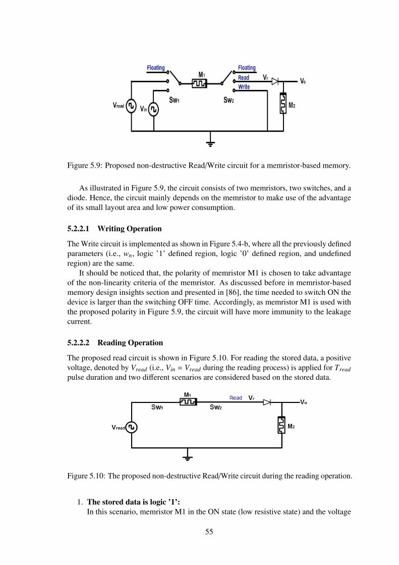
Figure 5.9: Proposed non-destructive Read/Write circuit for a memristor-based memory.
As illustrated in Figure 5.9, the circuit consists of two memristors, two switches, and adiode. Hence, the circuit mainly depends on the memristor to make use of the advantageof its small layout area and low power consumption.
5.2.2.1 Writing Operation
The Write circuit is implemented as shown in Figure 5.4-b, where all the previously definedparameters (i.e., wn, logic ’1’ defined region, logic ’0’ defined region, and undefinedregion) are the same.
It should be noticed that, the polarity of memristor M1 is chosen to take advantageof the non-linearity criteria of the memristor. As discussed before in memristor-basedmemory design insights section and presented in [86], the time needed to switch ON thedevice is larger than the switching OFF time. Accordingly, as memristor M1 is used withthe proposed polarity in Figure 5.9, the circuit will have more immunity to the leakagecurrent.
5.2.2.2 Reading Operation
The proposed read circuit is shown in Figure 5.10. For reading the stored data, a positivevoltage, denoted by Vread (i.e., Vin = Vread during the reading process) is applied for Treadpulse duration and two different scenarios are considered based on the stored data.
Figure 5.10: The proposed non-destructive Read/Write circuit during the reading operation.
1. The stored data is logic ’1’:In this scenario, memristor M1 in the ON state (low resistive state) and the voltage
55

drop on it is small and hence Vr almost equal to Vread which is designed largerthan 0.7V to allow the current to flow through the diode and memristor M2. InAs in the previous circuit, memristor M2 is used as a load resistor to get benefitof the memristor properties (i.e., small size, low power consumption, less heat,high resistivity in the OFF state, and compatibility with the circuit design) over theconventional resistor.
The output voltage drop on M2 (denoted by Vo) indicates which data is stored onthe memory cell (i.e., if Vo = VL, logic ’0’ is stored and if Vo = VH, logic ’1’ isstored). As noticed in Figure 5.10, memristor M2 is positioned to be always in thehigh resistive state. The output voltage, Vo = VH , is given by:
Vo(= VH) = Vr −n×VT × ln(Id
Isat)︸ ︷︷ ︸
Vd
= Id ×Ro f f |M2 (5.4)
where, Vo is the output voltage, Vd is the diode voltage drop, Id is the diode ONcurrent, Isat is the diode saturation current, n is the diode ideality factor, and VTis the thermal voltage (= KBT/q ≈ 26 mV at room temperature). The value of VHshould be designed as large as possible compared to VL.The value of Vo = VH should be designed as high as possible to distinguish readinglogic ’1’ state from reading logic ’0’ state (i.e., VH should be designed as large aspossible compared to VL). The utilization of memristor M2 in the high resistive statevalue provide a large load resistance which achieve this distinguishing objectiveeven for small Id values. The calculation of Vo = VH is obtained by solving thenonlinear equations given in (5.4) iteratively.
2. The stored data is logic ’0’:In this scenario, memristor M1 in the OFF state (high resistive state) and the voltagedrop on it is extremely large and hence Vr is very small. Vread is designed so thatafter the voltage drop on M1, Vr is less than 0.7V and hence the diode switches OFFand acts as an open circuit where no current flows through M2. Thus, the outputvoltage will be low (Vo = VL).
The non-destructive feature of the proposed circuit does exist because the readingvoltage will affect memristor M1 only during reading logic one, there will be no effectduring reading logic zero because the diode will act as an open circuit and hence no currentwill flow through the memory element (M1). As the circuit use a positive voltage to writelogic one then the reading voltage polarity and the writing voltage polarity is the same.The only main concern is to choose Vread so that it turns ON the diode while reading logicone and OFF while reading logic zero. Also, The diode is used to make sure that thecurrent flows through the load memristor M2 in one direction to maintain its OFF state andalso to provide immunity to the memory Read/Write circuit against the leakage currents.
56
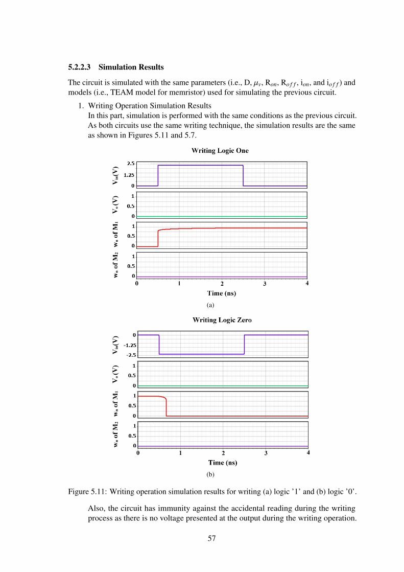
5.2.2.3 Simulation Results
The circuit is simulated with the same parameters (i.e., D, µv, Ron, Ro f f , ion, and io f f ) andmodels (i.e., TEAM model for memristor) used for simulating the previous circuit.
1. Writing Operation Simulation ResultsIn this part, simulation is performed with the same conditions as the previous circuit.As both circuits use the same writing technique, the simulation results are the sameas shown in Figures 5.11 and 5.7.
(a)
(b)
Figure 5.11: Writing operation simulation results for writing (a) logic ’1’ and (b) logic ’0’.
Also, the circuit has immunity against the accidental reading during the writingprocess as there is no voltage presented at the output during the writing operation.
57
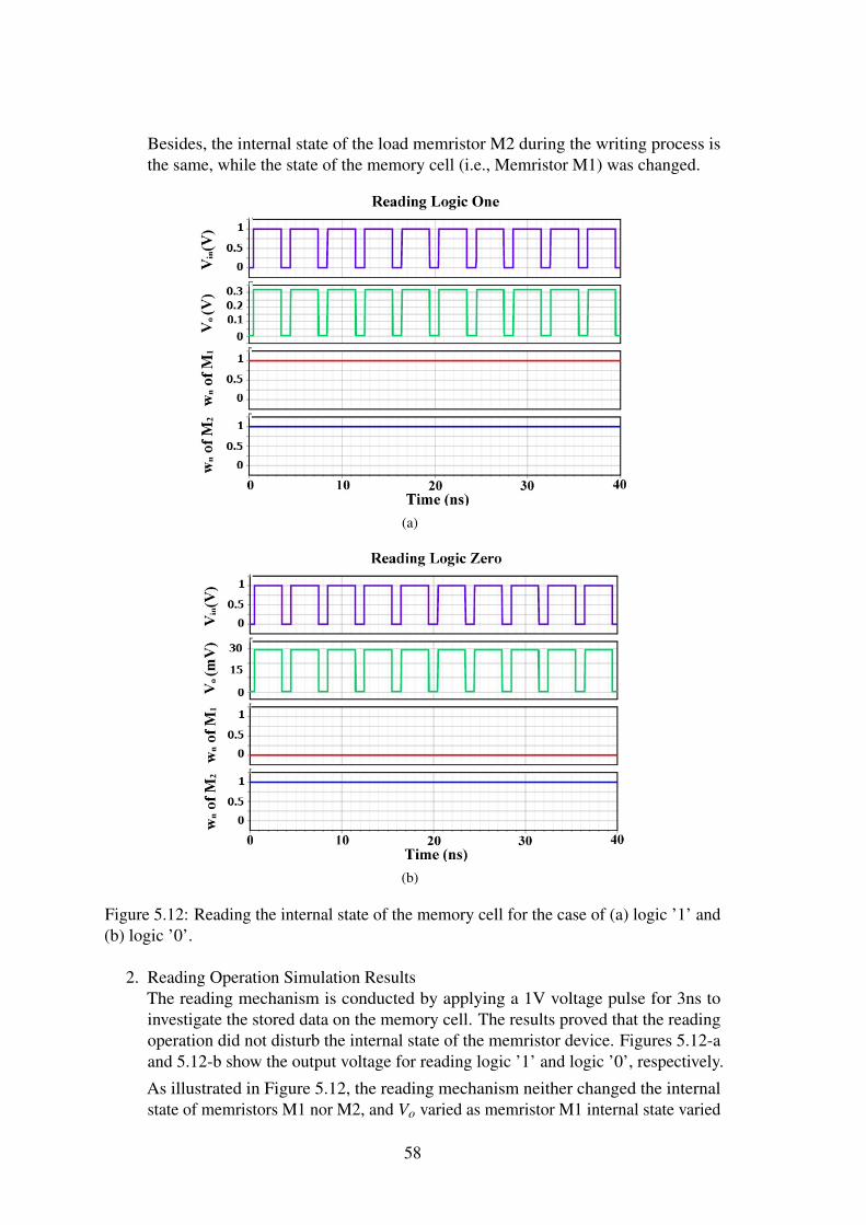
Besides, the internal state of the load memristor M2 during the writing process isthe same, while the state of the memory cell (i.e., Memristor M1) was changed.
(a)
(b)
Figure 5.12: Reading the internal state of the memory cell for the case of (a) logic ’1’ and(b) logic ’0’.
2. Reading Operation Simulation ResultsThe reading mechanism is conducted by applying a 1V voltage pulse for 3ns toinvestigate the stored data on the memory cell. The results proved that the readingoperation did not disturb the internal state of the memristor device. Figures 5.12-aand 5.12-b show the output voltage for reading logic ’1’ and logic ’0’, respectively.
As illustrated in Figure 5.12, the reading mechanism neither changed the internalstate of memristors M1 nor M2, and Vo varied as memristor M1 internal state varied
58
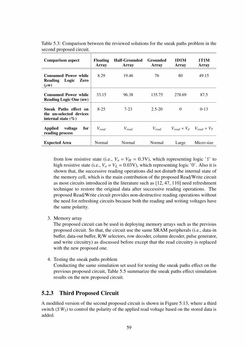
Table 5.3: Comparison between the reviewed solutions for the sneak paths problem in thesecond proposed circuit.
Comparison aspect Floating Half-Grounded Grounded 1D1M 1T1MArray Array Array Array Array
Consumed Power whileReading Logic Zero(µw)
8.29 19.46 76 80 49.15
Consumed Power whileReading Logic One (nw)
33.15 96.38 135.75 278.69 87.5
Sneak Paths effect onthe un-selected devicesinternal state (%)
8-25 7-23 2.5-20 0 0-13
Applied voltage forreading process
Vread Vread Vread Vread + Vd Vread + VT
Expected Area Normal Normal Normal Large Micro-size
from low resistive state (i.e., Vo = VH = 0.3V), which representing logic ’1’ tohigh resistive state (i.e., Vo = VL = 0.03V), which representing logic ’0’. Also it isshown that, the successive reading operations did not disturb the internal state ofthe memory cell, which is the main contribution of the proposed Read/Write circuitas most circuits introduced in the literature such as [12, 47, 110] need refreshmenttechnique to restore the original data after successive reading operations. Theproposed Read/Write circuit provides non-destructive reading operations withoutthe need for refreshing circuits because both the reading and writing voltages havethe same polarity.
3. Memory arrayThe proposed circuit can be used in deploying memory arrays such as the previousproposed circuit. So that, the circuit use the same SRAM peripherals (i.e., data-inbuffer, data-out buffer, R/W selectors, row decoder, column decoder, pulse generator,and write circuitry) as discussed before except that the read circuitry is replacedwith the new proposed one.
4. Testing the sneak paths problemConducting the same simulation set used for testing the sneak paths effect on theprevious proposed circuit, Table 5.5 summarize the sneak paths effect simulationresults on the new proposed circuit.
5.2.3 Third Proposed Circuit
A modified version of the second proposed circuit is shown in Figure 5.13, where a thirdswitch (S W3) to control the polarity of the applied read voltage based on the stored data isadded.
59
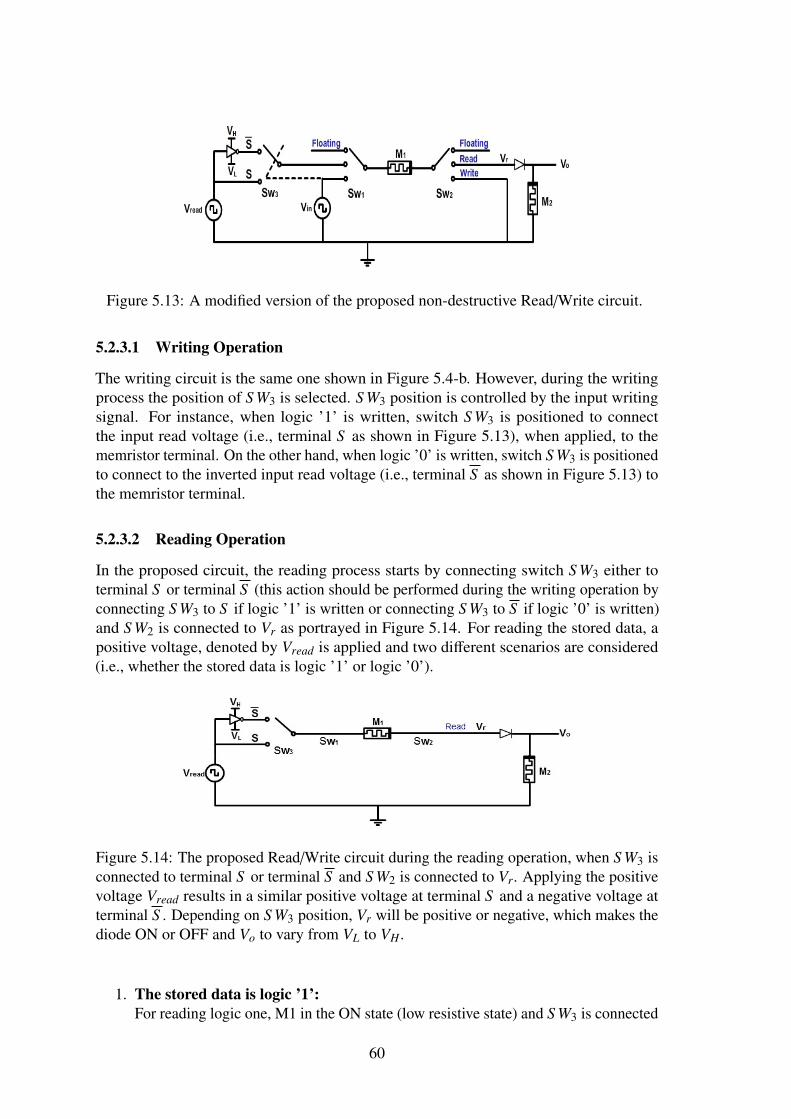
Figure 5.13: A modified version of the proposed non-destructive Read/Write circuit.
5.2.3.1 Writing Operation
The writing circuit is the same one shown in Figure 5.4-b. However, during the writingprocess the position of S W3 is selected. S W3 position is controlled by the input writingsignal. For instance, when logic ’1’ is written, switch S W3 is positioned to connectthe input read voltage (i.e., terminal S as shown in Figure 5.13), when applied, to thememristor terminal. On the other hand, when logic ’0’ is written, switch S W3 is positionedto connect to the inverted input read voltage (i.e., terminal S as shown in Figure 5.13) tothe memristor terminal.
5.2.3.2 Reading Operation
In the proposed circuit, the reading process starts by connecting switch S W3 either toterminal S or terminal S (this action should be performed during the writing operation byconnecting S W3 to S if logic ’1’ is written or connecting S W3 to S if logic ’0’ is written)and S W2 is connected to Vr as portrayed in Figure 5.14. For reading the stored data, apositive voltage, denoted by Vread is applied and two different scenarios are considered(i.e., whether the stored data is logic ’1’ or logic ’0’).
Figure 5.14: The proposed Read/Write circuit during the reading operation, when S W3 isconnected to terminal S or terminal S and S W2 is connected to Vr. Applying the positivevoltage Vread results in a similar positive voltage at terminal S and a negative voltage atterminal S . Depending on S W3 position, Vr will be positive or negative, which makes thediode ON or OFF and Vo to vary from VL to VH .
1. The stored data is logic ’1’:For reading logic one, M1 in the ON state (low resistive state) and S W3 is connected
60
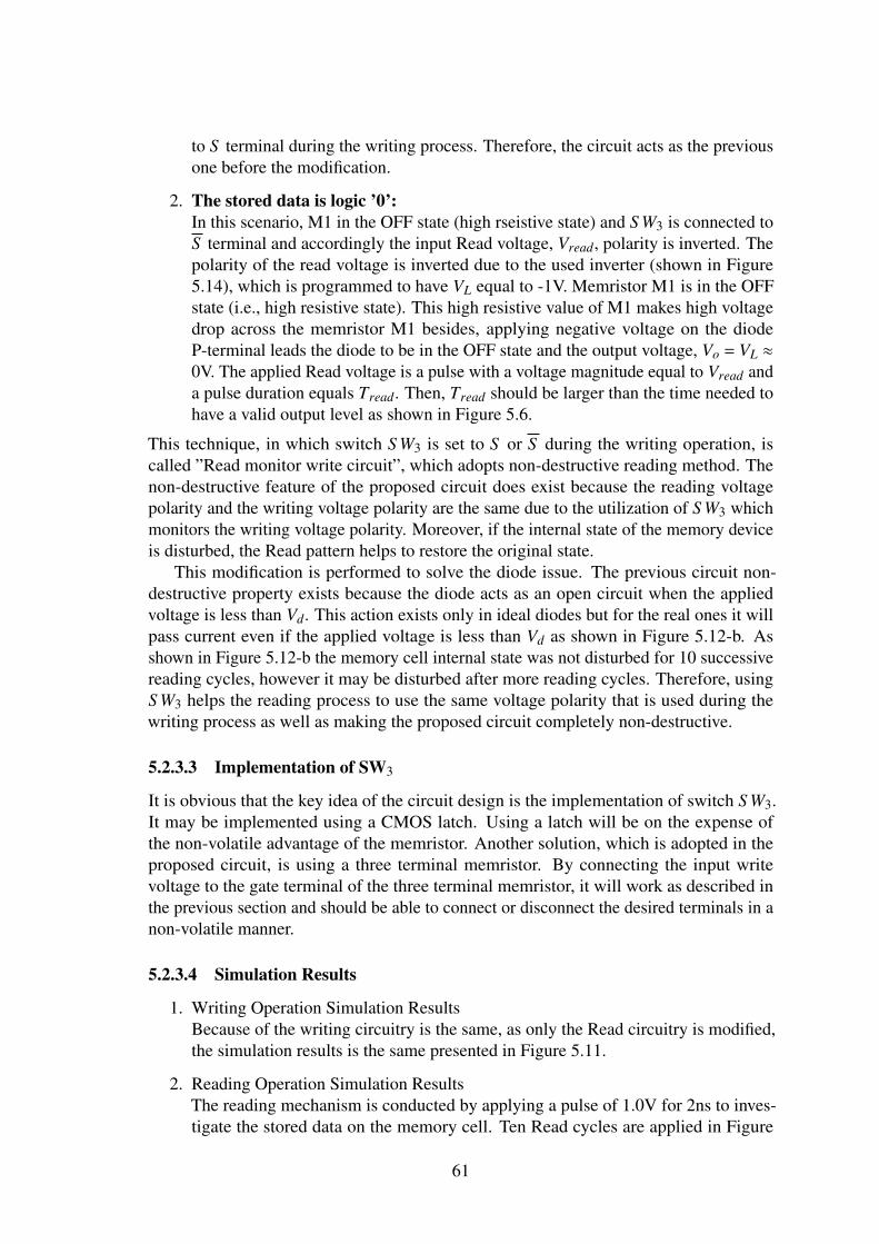
to S terminal during the writing process. Therefore, the circuit acts as the previousone before the modification.
2. The stored data is logic ’0’:In this scenario, M1 in the OFF state (high rseistive state) and S W3 is connected toS terminal and accordingly the input Read voltage, Vread, polarity is inverted. Thepolarity of the read voltage is inverted due to the used inverter (shown in Figure5.14), which is programmed to have VL equal to -1V. Memristor M1 is in the OFFstate (i.e., high resistive state). This high resistive value of M1 makes high voltagedrop across the memristor M1 besides, applying negative voltage on the diodeP-terminal leads the diode to be in the OFF state and the output voltage, Vo = VL ≈
0V. The applied Read voltage is a pulse with a voltage magnitude equal to Vread anda pulse duration equals Tread. Then, Tread should be larger than the time needed tohave a valid output level as shown in Figure 5.6.
This technique, in which switch S W3 is set to S or S during the writing operation, iscalled ”Read monitor write circuit”, which adopts non-destructive reading method. Thenon-destructive feature of the proposed circuit does exist because the reading voltagepolarity and the writing voltage polarity are the same due to the utilization of S W3 whichmonitors the writing voltage polarity. Moreover, if the internal state of the memory deviceis disturbed, the Read pattern helps to restore the original state.
This modification is performed to solve the diode issue. The previous circuit non-destructive property exists because the diode acts as an open circuit when the appliedvoltage is less than Vd. This action exists only in ideal diodes but for the real ones it willpass current even if the applied voltage is less than Vd as shown in Figure 5.12-b. Asshown in Figure 5.12-b the memory cell internal state was not disturbed for 10 successivereading cycles, however it may be disturbed after more reading cycles. Therefore, usingS W3 helps the reading process to use the same voltage polarity that is used during thewriting process as well as making the proposed circuit completely non-destructive.
5.2.3.3 Implementation of SW3
It is obvious that the key idea of the circuit design is the implementation of switch S W3.It may be implemented using a CMOS latch. Using a latch will be on the expense ofthe non-volatile advantage of the memristor. Another solution, which is adopted in theproposed circuit, is using a three terminal memristor. By connecting the input writevoltage to the gate terminal of the three terminal memristor, it will work as described inthe previous section and should be able to connect or disconnect the desired terminals in anon-volatile manner.
5.2.3.4 Simulation Results
1. Writing Operation Simulation ResultsBecause of the writing circuitry is the same, as only the Read circuitry is modified,the simulation results is the same presented in Figure 5.11.
2. Reading Operation Simulation ResultsThe reading mechanism is conducted by applying a pulse of 1.0V for 2ns to inves-tigate the stored data on the memory cell. Ten Read cycles are applied in Figure
61
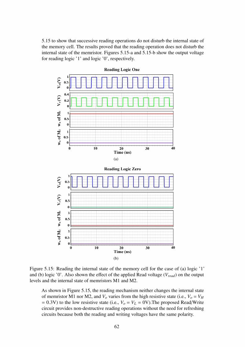
5.15 to show that successive reading operations do not disturb the internal state ofthe memory cell. The results proved that the reading operation does not disturb theinternal state of the memristor. Figures 5.15-a and 5.15-b show the output voltagefor reading logic ’1’ and logic ’0’, respectively.
(a)
(b)
Figure 5.15: Reading the internal state of the memory cell for the case of (a) logic ’1’and (b) logic ’0’. Also shown the effect of the applied Read voltage (Vread) on the outputlevels and the internal state of memristors M1 and M2.
As shown in Figure 5.15, the reading mechanism neither changes the internal stateof memristor M1 nor M2, and Vo varies from the high resistive state (i.e., Vo = VH= 0.3V) to the low resistive state (i.e., Vo = VL = 0V).The proposed Read/Writecircuit provides non-destructive reading operations without the need for refreshingcircuits because both the reading and writing voltages have the same polarity.
62
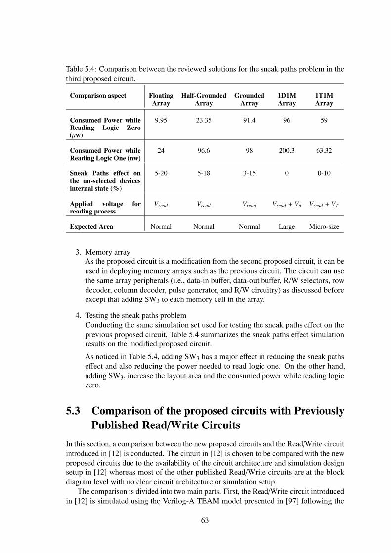
Table 5.4: Comparison between the reviewed solutions for the sneak paths problem in thethird proposed circuit.
Comparison aspect Floating Half-Grounded Grounded 1D1M 1T1MArray Array Array Array Array
Consumed Power whileReading Logic Zero(µw)
9.95 23.35 91.4 96 59
Consumed Power whileReading Logic One (nw)
24 96.6 98 200.3 63.32
Sneak Paths effect onthe un-selected devicesinternal state (%)
5-20 5-18 3-15 0 0-10
Applied voltage forreading process
Vread Vread Vread Vread + Vd Vread + VT
Expected Area Normal Normal Normal Large Micro-size
3. Memory arrayAs the proposed circuit is a modification from the second proposed circuit, it can beused in deploying memory arrays such as the previous circuit. The circuit can usethe same array peripherals (i.e., data-in buffer, data-out buffer, R/W selectors, rowdecoder, column decoder, pulse generator, and R/W circuitry) as discussed beforeexcept that adding SW3 to each memory cell in the array.
4. Testing the sneak paths problemConducting the same simulation set used for testing the sneak paths effect on theprevious proposed circuit, Table 5.4 summarizes the sneak paths effect simulationresults on the modified proposed circuit.
As noticed in Table 5.4, adding SW3 has a major effect in reducing the sneak pathseffect and also reducing the power needed to read logic one. On the other hand,adding SW3, increase the layout area and the consumed power while reading logiczero.
5.3 Comparison of the proposed circuits with PreviouslyPublished Read/Write Circuits
In this section, a comparison between the new proposed circuits and the Read/Write circuitintroduced in [12] is conducted. The circuit in [12] is chosen to be compared with the newproposed circuits due to the availability of the circuit architecture and simulation designsetup in [12] whereas most of the other published Read/Write circuits are at the blockdiagram level with no clear circuit architecture or simulation setup.
The comparison is divided into two main parts. First, the Read/Write circuit introducedin [12] is simulated using the Verilog-A TEAM model presented in [97] following the
63
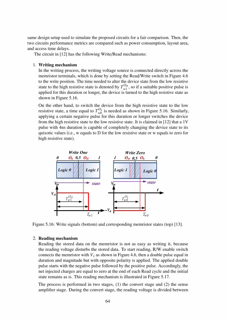
same design setup used to simulate the proposed circuits for a fair comparison. Then, thetwo circuits performance metrics are compared such as power consumption, layout area,and access time delays.
The circuit in [12] has the following Write/Read mechanisms:
1. Writing mechanismIn the writing process, the writing voltage source is connected directly across thememristor terminals, which is done by setting the Read/Write switch in Figure 4.6to the write position. The time needed to alter the device state from the low resistivestate to the high resistive state is denoted by T OH
w1 , so if a suitable positive pulse isapplied for this duration or longer, the device is turned to the high resistive state asshown in Figure 5.16.
On the other hand, to switch the device from the high resistive state to the lowresistive state, a time equal to T OL
w0 is needed as shown in Figure 5.16. Similarly,applying a certain negative pulse for this duration or longer switches the devicefrom the high resistive state to the low resistive state. It is claimed in [12] that a 1Vpulse with 4ns duration is capable of completely changing the device state to itsquixotic values (i.e., w equals to D for the low resistive state or w equals to zero forhigh resistive state).
Figure 5.16: Write signals (bottom) and corresponding memristor states (top) [13].
2. Reading mechanismReading the stored data on the memristor is not as easy as writing it, becausethe reading voltage disturbs the stored data. To start reading, R/W enable switchconnects the memristor with Vx as shown in Figure 4.6, then a double pulse equal induration and magnitude but with opposite polarity is applied. The applied doublepulse starts with the negative pulse followed by the positive pulse. Accordingly, thenet injected charges are equal to zero at the end of each Read cycle and the initialstate remains as is. This reading mechanism is illustrated in Figure 5.17.
The process is performed in two stages, (1) the convert stage and (2) the senseamplifier stage. During the convert stage, the reading voltage is divided between
64
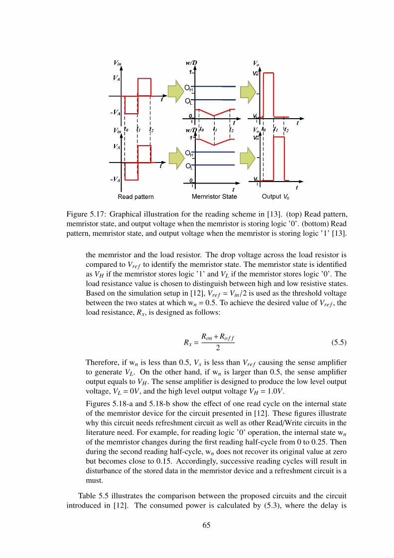
Figure 5.17: Graphical illustration for the reading scheme in [13]. (top) Read pattern,memristor state, and output voltage when the memristor is storing logic ’0’. (bottom) Readpattern, memristor state, and output voltage when the memristor is storing logic ’1’ [13].
the memristor and the load resistor. The drop voltage across the load resistor iscompared to Vre f to identify the memristor state. The memristor state is identifiedas VH if the memristor stores logic ’1’ and VL if the memristor stores logic ’0’. Theload resistance value is chosen to distinguish between high and low resistive states.Based on the simulation setup in [12], Vre f = Vin/2 is used as the threshold voltagebetween the two states at which wn = 0.5. To achieve the desired value of Vre f , theload resistance, Rx, is designed as follows:
Rx =Ron + Ro f f
2(5.5)
Therefore, if wn is less than 0.5, Vx is less than Vre f causing the sense amplifierto generate VL. On the other hand, if wn is larger than 0.5, the sense amplifieroutput equals to VH . The sense amplifier is designed to produce the low level outputvoltage, VL = 0V , and the high level output voltage VH = 1.0V .
Figures 5.18-a and 5.18-b show the effect of one read cycle on the internal stateof the memristor device for the circuit presented in [12]. These figures illustratewhy this circuit needs refreshment circuit as well as other Read/Write circuits in theliterature need. For example, for reading logic ’0’ operation, the internal state wnof the memristor changes during the first reading half-cycle from 0 to 0.25. Thenduring the second reading half-cycle, wn does not recover its original value at zerobut becomes close to 0.15. Accordingly, successive reading cycles will result indisturbance of the stored data in the memristor device and a refreshment circuit is amust.
Table 5.5 illustrates the comparison between the proposed circuits and the circuitintroduced in [12]. The consumed power is calculated by (5.3), where the delay is
65
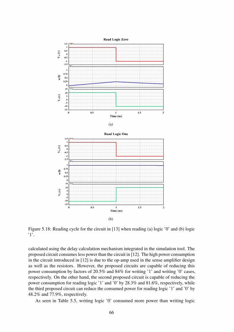
(a)
(b)
Figure 5.18: Reading cycle for the circuit in [13] when reading (a) logic ’0’ and (b) logic’1’.
calculated using the delay calculation mechanism integrated in the simulation tool. Theproposed circuit consumes less power than the circuit in [12]. The high power consumptionin the circuit introduced in [12] is due to the op-amp used in the sense amplifier designas well as the resistors. However, the proposed circuits are capable of reducing thispower consumption by factors of 20.5% and 84% for writing ’1’ and writing ’0’ cases,respectively. On the other hand, the second proposed circuit is capable of reducing thepower consumption for reading logic ’1’ and ’0’ by 28.3% and 81.6%, respectively, whilethe third proposed circuit can reduce the consumed power for reading logic ’1’ and ’0’ by48.2% and 77.9%, respectively.
As seen in Table 5.5, writing logic ’0’ consumed more power than writing logic
66
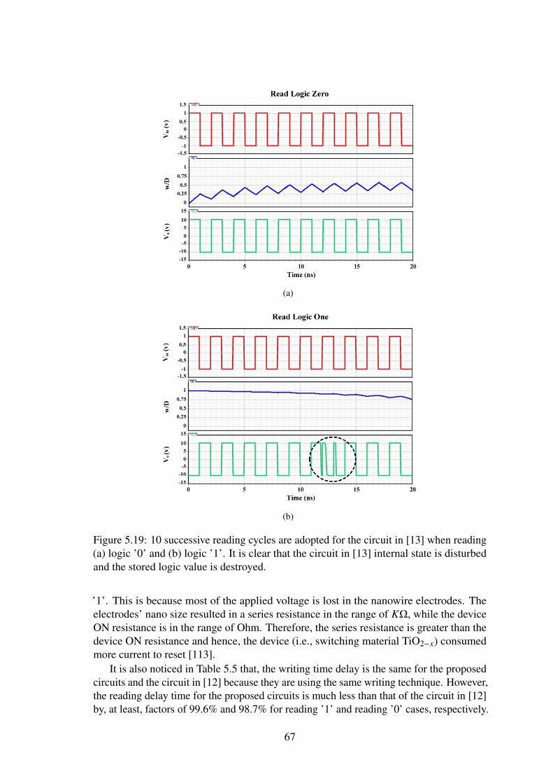
(a)
(b)
Figure 5.19: 10 successive reading cycles are adopted for the circuit in [13] when reading(a) logic ’0’ and (b) logic ’1’. It is clear that the circuit in [13] internal state is disturbedand the stored logic value is destroyed.
’1’. This is because most of the applied voltage is lost in the nanowire electrodes. Theelectrodes’ nano size resulted in a series resistance in the range of KΩ, while the deviceON resistance is in the range of Ohm. Therefore, the series resistance is greater than thedevice ON resistance and hence, the device (i.e., switching material TiO2−x) consumedmore current to reset [113].
It is also noticed in Table 5.5 that, the writing time delay is the same for the proposedcircuits and the circuit in [12] because they are using the same writing technique. However,the reading delay time for the proposed circuits is much less than that of the circuit in [12]by, at least, factors of 99.6% and 98.7% for reading ’1’ and reading ’0’ cases, respectively.
67
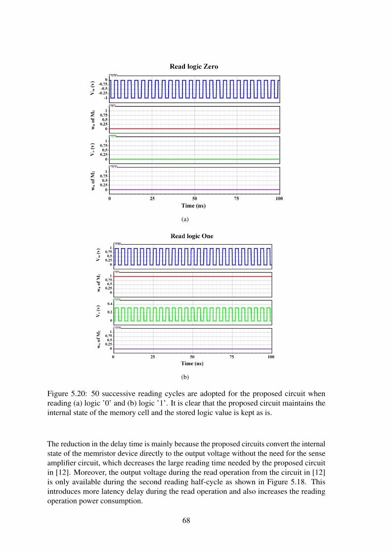
(a)
(b)
Figure 5.20: 50 successive reading cycles are adopted for the proposed circuit whenreading (a) logic ’0’ and (b) logic ’1’. It is clear that the proposed circuit maintains theinternal state of the memory cell and the stored logic value is kept as is.
The reduction in the delay time is mainly because the proposed circuits convert the internalstate of the memristor device directly to the output voltage without the need for the senseamplifier circuit, which decreases the large reading time needed by the proposed circuitin [12]. Moreover, the output voltage during the read operation from the circuit in [12]is only available during the second reading half-cycle as shown in Figure 5.18. Thisintroduces more latency delay during the read operation and also increases the readingoperation power consumption.
68
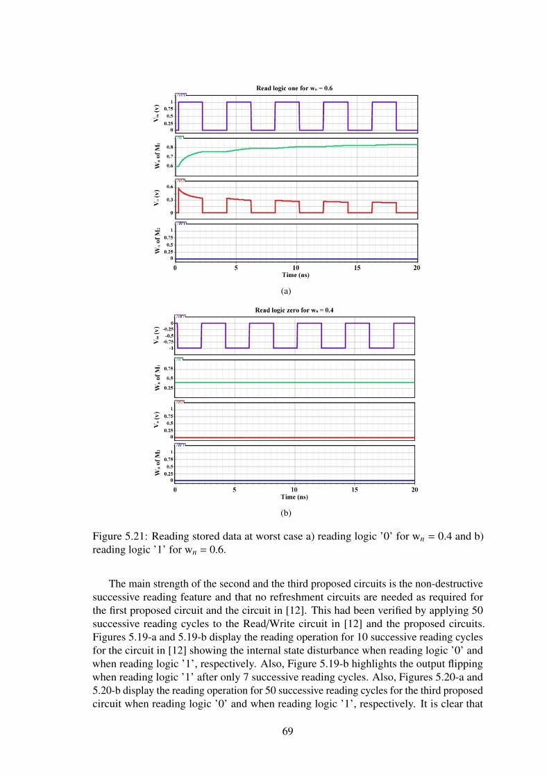
(a)
(b)
Figure 5.21: Reading stored data at worst case a) reading logic ’0’ for wn = 0.4 and b)reading logic ’1’ for wn = 0.6.
The main strength of the second and the third proposed circuits is the non-destructivesuccessive reading feature and that no refreshment circuits are needed as required forthe first proposed circuit and the circuit in [12]. This had been verified by applying 50successive reading cycles to the Read/Write circuit in [12] and the proposed circuits.Figures 5.19-a and 5.19-b display the reading operation for 10 successive reading cyclesfor the circuit in [12] showing the internal state disturbance when reading logic ’0’ andwhen reading logic ’1’, respectively. Also, Figure 5.19-b highlights the output flippingwhen reading logic ’1’ after only 7 successive reading cycles. Also, Figures 5.20-a and5.20-b display the reading operation for 50 successive reading cycles for the third proposedcircuit when reading logic ’0’ and when reading logic ’1’, respectively. It is clear that
69
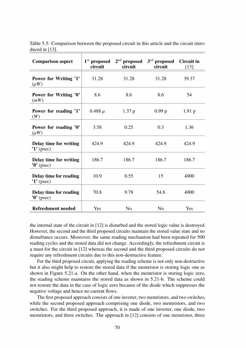
Table 5.5: Comparison between the proposed circuit in this article and the circuit intro-duced in [13].
Comparison aspect 1st proposed 2nd proposed 3rd proposed Circuit incircuit circuit circuit [13]
Power for Writing ’1’(µW)
31.28 31.28 31.28 39.37
Power for Writing ’0’(mW)
8.6 8.6 8.6 54
Power for reading ’1’(W)
0.488 µ 1.37 p 0.99 p 1.91 p
Power for reading ’0’(µW)
3.58 0.25 0.3 1.36
Delay time for writing’1’ (psec)
424.9 424.9 424.9 424.9
Delay time for writing’0’ (psec)
186.7 186.7 186.7 186.7
Delay time for reading’1’ (psec)
10.9 0.55 15 4000
Delay time for reading’0’ (psec)
70.8 9.78 54.8 4000
Refreshment needed Yes No No Yes
the internal state of the circuit in [12] is disturbed and the stored logic value is destroyed.However, the second and the third proposed circuits maintain the stored value state and nodisturbance occurs. Moreover, the same reading mechanism had been repeated for 500reading cycles and the stored data did not change. Accordingly, the refreshment circuit isa must for the circuit in [12] whereas the second and the third proposed circuits do notrequire any refreshment circuits due to this non-destructive feature.
For the third proposed circuit, applying the reading scheme is not only non-destructivebut it also might help to restore the stored data if the memristor is storing logic one asshown in Figure 5.21-a. On the other hand, when the memristor is storing logic zero,the reading scheme maintains the stored data as shown in 5.21-b. The scheme couldnot restore the data in the case of logic zero because of the diode which suppresses thenegative voltage and hence no current flows.
The first proposed approach consists of one inverter, two memristors, and two switches,while the second proposed approach comprising one diode, two memristors, and twoswitches. For the third proposed approach, it is made of one inverter, one diode, twomemristors, and three switches. The approach in [12] consists of one memristor, three
70

resistors, one comparator, and one switch. The layout area of the proposed designs areestimated to be 16.19 µm2 (i.e., 4.3µm2 (inverter) + 0.09 µm2 (two memristors) + 11.8µm2 (two switches)) for the first proposed circuit, 63.49 µm2 (i.e., 51.6µm2 (diode) +
0.09 µm2 (two memristors) + 11.8 µm2 (two switches)) for the second proposed circuit,and 73.79 µm2 (i.e., 4.3µm2 (inverter) + 51.6µm2 (diode) + 0.09 µm2 (two memristors) +
17.8 µm2 (three switches)). However, the estimated layout area of the design proposed in[12] equals 1841.645 µm2 (i.e., 0.045 µm2 (one memristor) + 135.7 µm2 (three resistors)+ 1700 µm2 (comparator) + 5.9 µm2 (one switch)). This illustrates how the proposedapproach reduces the area overhead of the R/W circuit by at least factor of 24X. The mainadvantage of the proposed designs is the exclusion of the comparator which occupies largelayout area.
71

72
Chapter 6: Discussion and Conclusions
6.1 Contributions
In this thesis, an overview of the physics behind different memristors types is discussedin light of the current state of the art and provides a comparative review between two ofthe most promising memristor physical realizations (i.e., TiO2 thin film memristor andspintronic memristor). The currently published memristor-based applications was reviewedshowing the importance of using memristors in memory applications. This importancecomes from the facts that, it is a straight forward application based on the memristorcharacteristics and leakage in the current memory technology to cover the huge storagecapabilities required by the nano-computing facilities. The current submitted Read/Writecircuits for memristor-based memory applications suffer from read-disturbance. This isbecause of the accumulative property of the device. Therefore, the reading voltage maydisturb the stored data. This problem is analyzed and memristor-based memory designinsights is introduced. Based on these insights, three novel designs of Read/Write circuitsfor memristor-based memory cell are proposed. Two of the proposed circuits have theadvantages of non-destructive successive reading cycles, less power consumption, lessdelay time, and smaller layout area, as compared to recently published Read/Write circuitin [12]. All these advantages are verified by comprehensive simulations by using CadenceSpectre while adopting TSMC 130nm industrial hardware-calibrated CMOS transistormodel card. The TEAM model had been used for the memristor device due to its accuracyand simplicity. The proposed circuits were tested for 500 successive read cycles where thestored data did not change. Besides, the proposed circuits reduce the power consumptionby factors of 20.5%, 84%, 77.9%, and 48.2% for writing ’1’, writing ’0’, reading ’1’, andreading ’0’ cases, respectively when compared with the circuit proposed in [12]. These isbecause the proposed circuits neither use comparator nor resistor. Moreover, the readingdelay time for the proposed circuit is much less than that of the circuit in [12] by factorsof 99.6% and 98.7% for reading ’1’ and reading ’0’ cases, respectively. It has been alsodemonstrated that the circuit in [12] does not maintain its stored data after 7 successivereading cycles (i.e., the stored data is flipped from logic ’1’ to logic ’0’) whereas theproposed circuits are capable of maintaining the stored data for large number of successivereading cycles (limited by the leakage current).
6.2 Published/Submitted papers
1. M. Elshamy, H. Mostafa, and M. Sameh Said, ”Comparative review of the TiO2and the spintronic memristor devices,” Canadian Conference on Electrical andComputer Engineering (CCECE’2014), Toronto, Canada, IEEE, pp. 317-322, 2014.
2. M. Elshamy, H. Mostafa, and M. Sameh Said, ”A novel non-destructive readout cir-cuit for memristor-based memory arrays,” IEEE Canadian Conference on Electricaland Computer Engineering (CCECE’2014), Toronto, Canada, IEEE, pp. 312-316,2014.
73
3. M. Elshamy, H. Mostafa, and M. Sameh Said, ”Design considerations/insights formemristor-based memory arrays,” IEEE International Conference on Engineeringand Technology (ICET’14), In Press (accepted in 21 Jan. 2014).
4. M. Elshamy, H. Mostafa, and M. Sameh Said, ”New non-destructive read/write cir-cuit for memristor-based memories,” IEEE International Conference on Engineeringand Technology (ICET’14), In Press (accepted in 21 Jan. 2014).
5. M. Elshamy, H. Mostafa, and M. Sameh Said, ”Novel non-destructive read/writecircuit for memristor-based memory arrays,” IEEE Transactions on Very LargeScale Integration Systems (TVLSI), In Press (accepted in 11 Nov. 2014).
6.3 Future WorkThis thesis provides a foundation for much future work in the areas of spintronic memristormodeling and design of memristor-based memory cells. For spintronic modeling, thedevice analysis and equations in this thesis are inconclusive, and so more analysis mustbe done to propose such a model. Another important modeling goal is to encapsulate theeffects of design variations for both spintronic and thin film TiO2 memristor; these effectsplay dominant role because of the nonlinear I-V curve for memristors, in particular theasymmetric ON/OFF switching time in the thin film TiO2 memristor and so these effectsneed to be modeled.With regards to the device analysis, as explained in Chapter 3, the device can be used inmulti-bit memory design. Alternative read and write techniques that would not disturb thestored data can be explored.Also, using memristor to build other architectures like FinFET need to be explored. Finally,fabrication of different test chips comprising the different proposed circuits and testing theread disturb immunity theorized in this work would be necessary.
74
References
[1] L. O. Chua, “Memristor-the missing circuit element,” IEEE Transaction CircuitsTheory, vol. 18, pp. 507–519, Septemper 1971.
[2] X. Wang and Y. Chen, “Patent relevant to spintronic memristor,” Recent Patent onElectrical Engineering, vol. 3, pp. 10–18, January 2010.
[3] L. O. Chua and S. M. Kang, “Memristive devices and systems,” Proc. IEEE, vol. 64,pp. 209–223, Febrauary 1976.
[4] L. O. Chua, “Device modeling via basic nonlinear circuit elements,” IEEE Transac-tion Circuits Systems, vol. CAS-27, pp. 1014–1044, November 1980.
[5] L. O. Chua, “Nonlinear circuits,” IEEE Transaction Circuits Systems, vol. CAS-31,pp. 69–87, January 1984.
[6] L. O. Chua, “Nonlinear circuit foundations for nanodevices, part I: The four-elementtorus,” Proc. IEEE, vol. 91, pp. 1830–1859, November 2003.
[7] M. Itoh and L. O. Chua, “Memristor oscillators,” J. Bifurcation Chaos, vol. 18,pp. 3183–3206, November 2008.
[8] M. D. Ventra, Y. V. Pershin, and L. O. Chua, “Circuit elements with memory:Memristors, memcapacitors and meminductors,” Proc. IEEE, vol. 97, pp. 1717–1724, October 2009.
[9] D. B. Strukov, G. S. Snider, D. R. Stewart, and R. S. Williams, “The missingmemristor found,” Nature, vol. 453, pp. 80–83, May 2008.
[10] R. S. Williams, “How we found the missing memristor,” Spectrum IEEE, vol. 45,pp. 28–35, December 2008.
[11] J. J. Yang, M. D. Picket, X. M. Li, D. A. A. Ohlberg, D. R. Stewart, and R. S.Williams, “Memristive switching mechanism for metal/oxide/metal nanodevices,”Nature Nanotechnology, vol. 3, pp. 429–433, July 2008.
[12] Y. Ho, G. M. Huang, and P. Li, “Dynamical properties and design analysis fornonvolatile memristor memories,” IEEE Transactions on Circuits and Systems I,vol. 58, pp. 724–736, April 2011.
[13] Erokhin, Victor, Fontana, and P. Marco, “Electrochemically controlled polymericdevice: a memristor (and more) found two years ago,” July 2008.
[14] M. Crupi, L. Pradhan, and S. Tozer, “Modelling neural plasticity with memristors,”IEEE Canadian Review, pp. 10–14, 2012.
75
[15] A. Chanthbouala, V. Garcia, R. O. Cherifi, K. Bouzehouane, S. Fusil, X. Moya,S. Xavier, H. Yamada, C. Deranlot, N. D. Mathur, M. Bibes, A. Barthlmy, andJ. Grollier, “A ferroelectric memristor,” Nature Materials, vol. 11, pp. 860–864,Septemper 2012.
[16] X. Wang, Y. Chen, H. Xi, H. Li, and D. Dimitrov, “Spintronic memristor throughspin-torque-induced magnetization motion,” IEEE Electron Device Letter, vol. 30,pp. 294–297, March 2009.
[17] Y. Chen and X.Wang, “Compact modeling and corner analysis of spintronic mem-ristor,” Proc. Int. Symp. IEEE/ACM NANOARCH, pp. 7–12, March 2009.
[18] J. Borghetti, Z. Li, J. Straznicky, X. Li, D. A. A. Ohlberg, W.Wu, D. R. Stewart,and R. S.Williams, “A hybrid nanomemristor/transistor logic circuit capable ofself-programming,” Proc. Nat. Acad. Sci. USA, vol. 106, pp. 1699–1703, February2009.
[19] G. Snider, P. Kuekes, and R. S. Williams, “CMOS-like logic in defective, nanoscalecrossbars,” Nature Nanotechnology, vol. 15, pp. 881–891, June 2004.
[20] O. Kavehei, Y. Kim, A. Iqbal, K. Eshraghiam, S. F. Al-Sarawi, and D. Abbott,“The fourth element: Characteristics, modelling, and electromagnetic theory ofthe memristor,” Proceeding of the Royal Society A-Mathematical Physical andEngineering Sciences, vol. 466, pp. 2175–2202, August 2010.
[21] International Technology Roadmap for Semiconductor, 2010.
[22] P. J. Kuekes, D. R. Stewart, and R. S. Williams, “The crossbar latch: Logic valuestorage, restoration, and inversion in crossbar circuits,” Journal of Applied Physics,vol. 97, pp. 034301–034301–5, February 2005.
[23] T. Raja and S. Mourad, “Digital logic implementation in memristor-based crossbar,”International Conference on Communications, Circuits and Systems (ICCCAS),pp. 23–25, July 2009.
[24] J. Borghetti, G. S. Snider, P. J. Kuekes, J. J. Yang, D. R. Stewart, and R. S. Williams,“’memristive’ switches enable ’stateful’ logic operations via material implication,”Nature, vol. 464, pp. 873–876, April 2010.
[25] E. Lehtonen and M. Laiho, “Stateful implication logic with memristors,” Interna-tional Symposium on Nanoscale Architecture, pp. 33–36, July 2009.
[26] Y. Pershin and M. D. Ventra, “Practical approach to programmable analog circuitwith memristors,” IEEE Transaction on Circuits Systems I, vol. 57, pp. 1857–1864,August 2009.
[27] M. Laiho and E. Lehtonen, “Arithmetic operations within memristor based analogmemory,” International Workshop on Cellular Nanoscale Networks and TheirApplications (CNNA), pp. 1–6, February 2010.
76
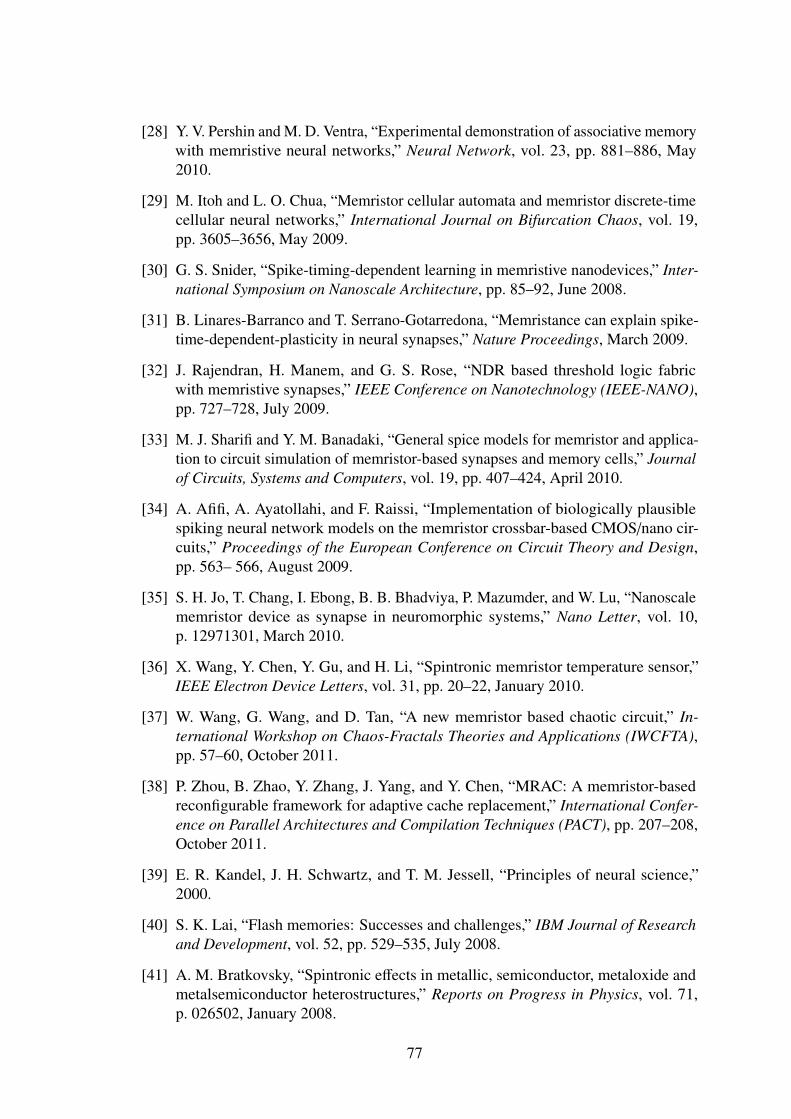
[28] Y. V. Pershin and M. D. Ventra, “Experimental demonstration of associative memorywith memristive neural networks,” Neural Network, vol. 23, pp. 881–886, May2010.
[29] M. Itoh and L. O. Chua, “Memristor cellular automata and memristor discrete-timecellular neural networks,” International Journal on Bifurcation Chaos, vol. 19,pp. 3605–3656, May 2009.
[30] G. S. Snider, “Spike-timing-dependent learning in memristive nanodevices,” Inter-national Symposium on Nanoscale Architecture, pp. 85–92, June 2008.
[31] B. Linares-Barranco and T. Serrano-Gotarredona, “Memristance can explain spike-time-dependent-plasticity in neural synapses,” Nature Proceedings, March 2009.
[32] J. Rajendran, H. Manem, and G. S. Rose, “NDR based threshold logic fabricwith memristive synapses,” IEEE Conference on Nanotechnology (IEEE-NANO),pp. 727–728, July 2009.
[33] M. J. Sharifi and Y. M. Banadaki, “General spice models for memristor and applica-tion to circuit simulation of memristor-based synapses and memory cells,” Journalof Circuits, Systems and Computers, vol. 19, pp. 407–424, April 2010.
[34] A. Afifi, A. Ayatollahi, and F. Raissi, “Implementation of biologically plausiblespiking neural network models on the memristor crossbar-based CMOS/nano cir-cuits,” Proceedings of the European Conference on Circuit Theory and Design,pp. 563– 566, August 2009.
[35] S. H. Jo, T. Chang, I. Ebong, B. B. Bhadviya, P. Mazumder, and W. Lu, “Nanoscalememristor device as synapse in neuromorphic systems,” Nano Letter, vol. 10,p. 12971301, March 2010.
[36] X. Wang, Y. Chen, Y. Gu, and H. Li, “Spintronic memristor temperature sensor,”IEEE Electron Device Letters, vol. 31, pp. 20–22, January 2010.
[37] W. Wang, G. Wang, and D. Tan, “A new memristor based chaotic circuit,” In-ternational Workshop on Chaos-Fractals Theories and Applications (IWCFTA),pp. 57–60, October 2011.
[38] P. Zhou, B. Zhao, Y. Zhang, J. Yang, and Y. Chen, “MRAC: A memristor-basedreconfigurable framework for adaptive cache replacement,” International Confer-ence on Parallel Architectures and Compilation Techniques (PACT), pp. 207–208,October 2011.
[39] E. R. Kandel, J. H. Schwartz, and T. M. Jessell, “Principles of neural science,”2000.
[40] S. K. Lai, “Flash memories: Successes and challenges,” IBM Journal of Researchand Development, vol. 52, pp. 529–535, July 2008.
[41] A. M. Bratkovsky, “Spintronic effects in metallic, semiconductor, metaloxide andmetalsemiconductor heterostructures,” Reports on Progress in Physics, vol. 71,p. 026502, January 2008.
77
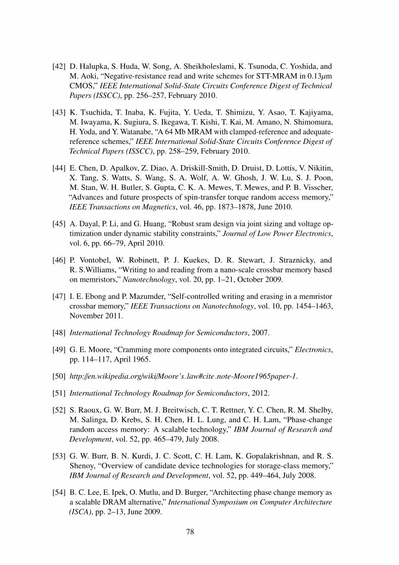
[42] D. Halupka, S. Huda, W. Song, A. Sheikholeslami, K. Tsunoda, C. Yoshida, andM. Aoki, “Negative-resistance read and write schemes for STT-MRAM in 0.13µmCMOS,” IEEE International Solid-State Circuits Conference Digest of TechnicalPapers (ISSCC), pp. 256–257, February 2010.
[43] K. Tsuchida, T. Inaba, K. Fujita, Y. Ueda, T. Shimizu, Y. Asao, T. Kajiyama,M. Iwayama, K. Sugiura, S. Ikegawa, T. Kishi, T. Kai, M. Amano, N. Shimomura,H. Yoda, and Y. Watanabe, “A 64 Mb MRAM with clamped-reference and adequate-reference schemes,” IEEE International Solid-State Circuits Conference Digest ofTechnical Papers (ISSCC), pp. 258–259, February 2010.
[44] E. Chen, D. Apalkov, Z. Diao, A. Driskill-Smith, D. Druist, D. Lottis, V. Nikitin,X. Tang, S. Watts, S. Wang, S. A. Wolf, A. W. Ghosh, J. W. Lu, S. J. Poon,M. Stan, W. H. Butler, S. Gupta, C. K. A. Mewes, T. Mewes, and P. B. Visscher,“Advances and future prospects of spin-transfer torque random access memory,”IEEE Transactions on Magnetics, vol. 46, pp. 1873–1878, June 2010.
[45] A. Dayal, P. Li, and G. Huang, “Robust sram design via joint sizing and voltage op-timization under dynamic stability constraints,” Journal of Low Power Electronics,vol. 6, pp. 66–79, April 2010.
[46] P. Vontobel, W. Robinett, P. J. Kuekes, D. R. Stewart, J. Straznicky, andR. S.Williams, “Writing to and reading from a nano-scale crossbar memory basedon memristors,” Nanotechnology, vol. 20, pp. 1–21, October 2009.
[47] I. E. Ebong and P. Mazumder, “Self-controlled writing and erasing in a memristorcrossbar memory,” IEEE Transactions on Nanotechnology, vol. 10, pp. 1454–1463,November 2011.
[48] International Technology Roadmap for Semiconductors, 2007.
[49] G. E. Moore, “Cramming more components onto integrated circuits,” Electronics,pp. 114–117, April 1965.
[50] http://en.wikipedia.org/wiki/Moore’s law#cite note-Moore1965paper-1.
[51] International Technology Roadmap for Semiconductors, 2012.
[52] S. Raoux, G. W. Burr, M. J. Breitwisch, C. T. Rettner, Y. C. Chen, R. M. Shelby,M. Salinga, D. Krebs, S. H. Chen, H. L. Lung, and C. H. Lam, “Phase-changerandom access memory: A scalable technology,” IBM Journal of Research andDevelopment, vol. 52, pp. 465–479, July 2008.
[53] G. W. Burr, B. N. Kurdi, J. C. Scott, C. H. Lam, K. Gopalakrishnan, and R. S.Shenoy, “Overview of candidate device technologies for storage-class memory,”IBM Journal of Research and Development, vol. 52, pp. 449–464, July 2008.
[54] B. C. Lee, E. Ipek, O. Mutlu, and D. Burger, “Architecting phase change memory asa scalable DRAM alternative,” International Symposium on Computer Architecture(ISCA), pp. 2–13, June 2009.
78
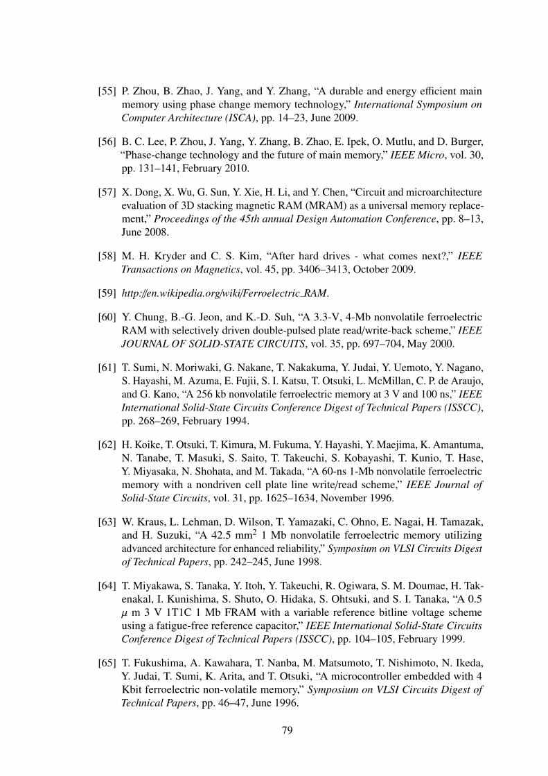
[55] P. Zhou, B. Zhao, J. Yang, and Y. Zhang, “A durable and energy efficient mainmemory using phase change memory technology,” International Symposium onComputer Architecture (ISCA), pp. 14–23, June 2009.
[56] B. C. Lee, P. Zhou, J. Yang, Y. Zhang, B. Zhao, E. Ipek, O. Mutlu, and D. Burger,“Phase-change technology and the future of main memory,” IEEE Micro, vol. 30,pp. 131–141, February 2010.
[57] X. Dong, X. Wu, G. Sun, Y. Xie, H. Li, and Y. Chen, “Circuit and microarchitectureevaluation of 3D stacking magnetic RAM (MRAM) as a universal memory replace-ment,” Proceedings of the 45th annual Design Automation Conference, pp. 8–13,June 2008.
[58] M. H. Kryder and C. S. Kim, “After hard drives - what comes next?,” IEEETransactions on Magnetics, vol. 45, pp. 3406–3413, October 2009.
[59] http://en.wikipedia.org/wiki/Ferroelectric RAM.
[60] Y. Chung, B.-G. Jeon, and K.-D. Suh, “A 3.3-V, 4-Mb nonvolatile ferroelectricRAM with selectively driven double-pulsed plate read/write-back scheme,” IEEEJOURNAL OF SOLID-STATE CIRCUITS, vol. 35, pp. 697–704, May 2000.
[61] T. Sumi, N. Moriwaki, G. Nakane, T. Nakakuma, Y. Judai, Y. Uemoto, Y. Nagano,S. Hayashi, M. Azuma, E. Fujii, S. I. Katsu, T. Otsuki, L. McMillan, C. P. de Araujo,and G. Kano, “A 256 kb nonvolatile ferroelectric memory at 3 V and 100 ns,” IEEEInternational Solid-State Circuits Conference Digest of Technical Papers (ISSCC),pp. 268–269, February 1994.
[62] H. Koike, T. Otsuki, T. Kimura, M. Fukuma, Y. Hayashi, Y. Maejima, K. Amantuma,N. Tanabe, T. Masuki, S. Saito, T. Takeuchi, S. Kobayashi, T. Kunio, T. Hase,Y. Miyasaka, N. Shohata, and M. Takada, “A 60-ns 1-Mb nonvolatile ferroelectricmemory with a nondriven cell plate line write/read scheme,” IEEE Journal ofSolid-State Circuits, vol. 31, pp. 1625–1634, November 1996.
[63] W. Kraus, L. Lehman, D. Wilson, T. Yamazaki, C. Ohno, E. Nagai, H. Tamazak,and H. Suzuki, “A 42.5 mm2 1 Mb nonvolatile ferroelectric memory utilizingadvanced architecture for enhanced reliability,” Symposium on VLSI Circuits Digestof Technical Papers, pp. 242–245, June 1998.
[64] T. Miyakawa, S. Tanaka, Y. Itoh, Y. Takeuchi, R. Ogiwara, S. M. Doumae, H. Tak-enakal, I. Kunishima, S. Shuto, O. Hidaka, S. Ohtsuki, and S. I. Tanaka, “A 0.5µ m 3 V 1T1C 1 Mb FRAM with a variable reference bitline voltage schemeusing a fatigue-free reference capacitor,” IEEE International Solid-State CircuitsConference Digest of Technical Papers (ISSCC), pp. 104–105, February 1999.
[65] T. Fukushima, A. Kawahara, T. Nanba, M. Matsumoto, T. Nishimoto, N. Ikeda,Y. Judai, T. Sumi, K. Arita, and T. Otsuki, “A microcontroller embedded with 4Kbit ferroelectric non-volatile memory,” Symposium on VLSI Circuits Digest ofTechnical Papers, pp. 46–47, June 1996.
79
[66] M.A.Zidan, H. A. H. Fahmy, M. M. Hussain, and K. N. Salama, “Memristor-based memory: The sneak paths problem and solutions,” Microelectronics Journal,pp. 176–183, February 2013.
[67] T. Perez and C. Rose, “Non-volatile memory: Emerging technologies and theirimpacts on memory systems,” Technical Report, September 2010.
[68] K. Witrisal, “Memristor-based stored-reference receiver - the UWB solution?,”Electronics Letters, vol. 45, pp. 713–714, July 2009.
[69] M. Crupi, L. Pradhan, and S. Tozer, “Modelling neural plasticity with memristors,”IEEE Canadian Review, vol. 68, pp. 10–14, 2012.
[70] T. W. Hickmott, “Low-frequency negative resistance in thin anodic oxide films,”Journal of Applied Physics, vol. 33, p. 2669, February 1962.
[71] J. G. Simmons and R. R. Verderber, “New conduction and reversible memoryphenomena in thin insulating films,” Proceedings of the Royal Society A, pp. 77–102, October 1967.
[72] F. Argall, “Switching phenomena in titanium oxide thin films,” Solid State Elec-tronics, vol. 11, pp. 535–541, May 1968.
[73] T. Driscoll, H.-T. Kim, B.-G. Chae, M. D. Ventra, and D. N. Basov, “Phase-transition driven memristive system,” Applied Physics Letters, vol. 95, pp. 043503–1–3, July 2009.
[74] T. Driscoll, H.-T. Kim, B.-G. Chae, B.-J. Kim, Y.-W. Lee, N. M. Jokerst, S. Palit,D. R. Smith, M. D. Ventra, and D. N. Basov, “Memory metamaterials,” Science,vol. 325, pp. 1518–1521, September 2009.
[75] A. S. Alexandrov and A. M. Bratkovsky, “Polaronic memory resistors stronglycoupled to electrodes,” Physical Review B, vol. 80, p. 115321, September 2009.
[76] J. H. Krieger and S. M. Spitzer, “Non-traditional, non-volatile memory based onswitching and retention phenomena in polymeric thin films,” Non-Volatile MemoryTechnology Symposium, pp. 121–124, 2004.
[77] D. S. Kim, Y. H. Kim, C. E. Lee, and Y. T. Kim, “Colossal electroresistancemechanism in a Au/Pr0.7Ca0.3MnO3/Pt sandwich structure: Evidence for a motttransition,” Physical Review B, vol. 74, p. 174430, November 2006.
[78] M. Quintero, P. Levy, A. G. Leyva, and M. J. Rozenberg, “Mechanism of electric-pulse-induced resistance switching in manganites,” Physical Review Letters, vol. 98,p. 116601, March 2007.
[79] E. Arcangeletti, L. Baldassarre, D. D. Castro, S. Lupi, L. Malavasi, C. Marini,A. Perucchi, and P. Postorino, “Evidence of a pressure-induced metallization processin monoclinic VO2,” Physical Review Letters, vol. 98, p. 196406, May 2007.
80
[80] M. M. Qazilbash, A. A. Schafgans, K. S. Burch, S. J. Yun, B. G. Chae, B. J. Kim,H. T. Kim, and D. N. Basov, “Electrodynamics of the vanadium oxides VO2 andV2O3,” Physical Review B, vol. 77, p. 115121, March 2008.
[81] Y. V. Pershin and M. D. Ventra, “Memory effects in complex materials and nanoscalesystems,” Advances in Physics, vol. 60, pp. 145–227, November 2011.
[82] A. Sharoni, J. G. Ramrez, and I. K. Schuller, “Multiple avalanches across the metal-insulator transition of vanadium oxide nanoscaled junctions,” Physical ReviewLetters, vol. 101, p. 026404, July 2008.
[83] Z. B. Yan, K. F. Wang, S. Z. Li, S. J. Luo, and J.-M. Liu, “Reversible resistanceswitching in La0.225Pr0.4Ca0.375MnO3: The joule-heat-assisted phase transition,”Applied Physics Letters, vol. 95, p. 143502, October 2009.
[84] N. Gergel-Hackett, B. Hamadani, B. Dunlap, J. Suehle, C. Richter, C. Hacker, andD. Gundlach, “A flexible solution-processed memristor,” IEEE Electron DeviceLetters, vol. 30, pp. 706–708, July 2009.
[85] Y. Ho, G. Huang, and P. Li, “Nonvolatile memristor memory: Device characteris-tics and design implications,” Proc. IEEE/ACMInt. Conf. Comput. Aided Design(ICCAD), pp. 485–490, November 2009.
[86] M. D. Pickett, D. B. Strukov, J. L. Borghetti, J. J. Yang, G. S. Snider, D. R. Stewart,and R. S. Williams, “Switching dynamics in titanium dioxide memristive devices,”Journal of Applied Physics, vol. 106, pp. 1–6, October 2009.
[87] W. Yi, F. Perner, M. S. Qureshi, H. Abdalla, M. D. Pickett, J. J. Yang, M.-X. M.Zhang, G. Mederios-Ribeiro, and R. S. Williams, “Feedback write scheme formemristive switching devices,” Applied Physics A, vol. 102, pp. 973–982, March2011.
[88] H. Akimoto, H. Kanai, Y. Uehara, T. Ishizuka, and S. Kameyama, “Analysisof thermal magnetic noise in spin-valve GMR heads by using micromagneticsimulation,” Journal of Applied Physics, vol. 97, p. 10N705, May 2005.
[89] M. A. Mohamed, N. Inami, E. Shikoh, Y. Yamamoto, H. Hori, and A. Fujiwara,“Fabrication of spintronic device by direct synthesis of single-walled carbon nan-otubes from ferromagnetic electrodes,” Science and Technology of Advanced Mate-rials, vol. 9, pp. 1–5, July 2008.
[90] M. Hu, H. Li, Y. Chen, X. Wang, and R. E. Pino, “Geometry variations analysis ofTiO2 thin-film and spintronic memristors,” IEEE Design Automation Conference(ASP-DAC), pp. 25–30, January 2011.
[91] D. Batas and H. Fiedler, “A memristor spice implementation and a new approachfor magnetic flux-controlled memristor modelling,” IEEE Transactions on Nan-otechnology, vol. 10, pp. 250–255, March 2011.
81
[92] H. Elgabra, I. A. Farhat, A. S. A. Hosani, D. Homouz, and B. Mohammad, “Mathe-matical modeling of a memristor device,” International Conference on Innovationsin Information Technology (IIT), pp. 156–161, March 2012.
[93] M. Mahvash and A. C. Parker, “A memristor SPICE model for designing memristorcircuits,” IEEE International Midwest Symposium on Circuits and Systems, pp. 989–992, August 2010.
[94] A. Rak and G. Cserey, “Macromodeling of the memristor in SPICE,” IEEE Trans-actions on Computer-Aided Design of Integrated Circuits and Systems, vol. 29,pp. 632–636, April 2010.
[95] Z. Biolek, D. Biolek, and V. Biolkova, “Spice model of memristor with nonlineardopant drift,” radio engineering, vol. 18, pp. 210–214, 2009.
[96] H. Abdalla and M. D. Pickett, “Spice modeling of memristors,” IEEE InternationalSymposium on Circuits and Systems, pp. 1832–1835, May 2011.
[97] S. Kvatinsky, E. G. Friedman, A. Kolodny, and U. C. Weiser, “TEAM: Thresholdadaptive memristor model,” IEEE Transactions on Circuits and Systems I, vol. 60,pp. 211–221, January 2013.
[98] A. C. Cabe and S. Das, “Performance simulation and analysis of a CMOS/nanohybrid nano processor system,” Nanotechnology, vol. 20, p. 165203, March 2009.
[99] S. H. Jo, T. Chang, I. Ebong, B. B. Bhadviya, and P. Mazumder, “Nanoscalememristor device as synapse in neuromorphic systems,” Nano Letters, vol. 10,pp. 1297–1301, March 2010.
[100] F. Alibart, S. Pleutin, D. Guerin, C. Novembre, S. Lenfant, K. Lmimouni, C. Gamrat,and D. Vuillaume, “An organic nanoparticle transistor behaving as a biologicalspiking synapse,” Advanced Functional Materials, vol. 20, pp. 330–337, January2010.
[101] C. Yakopcic, T. M. Taha, G. Subramanyam, and S. Rogers, “Multiple memristorread and write circuit for neuromorphic applications,” Proceedings of InternationalJoint Conference on Neural Networks, pp. 2676–2682, July-August 2011.
[102] S.-M. K. S. Shin, K. Kim, “Memristor applications for programmable analog ICs,”IEEE Transactions on Nanotechnology, vol. 10, pp. 266–274, March 2011.
[103] D. B. Strukov and K. K. Likharev, “Reconfigurable hybrid CMOS/nanodevicecircuits for image processing,” IEEE Transactions on Nanotechnology, vol. 6,pp. 696–710, November 2007.
[104] D. Strukov and K. Likharev, “CMOL FPGA: A cell-based, reconfigurable architec-ture for hybrid digital circuits using two-terminal nanodevices,” Nanotechnology,vol. 16, pp. 888–900, April 2005.
[105] J. G. Simmons, “Generalized formula for the electric tunnel effect between similarelectrodes separated by a thin insulating film,” Journal of Applied Physics, vol. 34,pp. 1793–1803, January 1963.
82
[106] G. S. Snider, “Cortical computing with memristive nanodevices,” SciDAC Review,vol. 10, pp. 58–65, 2008.
[107] R. C. Froemke and Y. Dan, “Spike timing-dependent synaptic modification inducedby natural spike trains nature,” Nature, vol. 416, pp. 433–438, January 2002.
[108] Y. V. Pershin and M. D. Ventra, “Neuromorphic, digital, and quantum computationwith memory circuit elements,” Proceedings of the IEEE, vol. 100, pp. 2071–2080,June 2012.
[109] J. Cong and B. Xiao, “mrFPGA: A novel FPGA architecture with memristor-basedreconfiguration,” IEEE/ACM International Symposium on Nanoscale Architectures(NANOARCH), pp. 1–8, June 2011.
[110] D. Niu, Y. Chen, and Y. Xie, “Low-power dual-element memristor based memorydesign,” International Symposium on Low-Power Electronics and Design (ISLPED),pp. 25–30, August 2010.
[111] H. Kim, M. P. Sah, C. Yang, and L. O. Chua, “Memristor-based multilevel memory,”International Workshop on Cellular Nanoscale Networks and their Applications(CNNA), pp. 1–6, February 2010.
[112] H. Manem and G. S. Rose, “A read-monitored write circuit for 1T1M multi-levelmemristor memories,” IEEE International Symposium on Circuits and Systems(ISCAS), May 2011.
[113] Q. Xia, M. D. Pickett, J. J. Yang, X. Li, W. Wu, G. Medeiros-Ribeiro, and R. S.Williams, “Two- and three-terminal resistive switches: Nanometer-scale memristorsand memistors,” Advanced Functional Materials, vol. 21, pp. 2660–2665, July2011.
[114] D. B. Strukov, J. L. Borghetti, and R. S. Williams, “Coupled ionic and electronictransport model of thin-film semiconductor memristive behavior,” Small, vol. 5,pp. 1058–1063, May 2009.
[115] M. J. Lee, Y. Park, B. S. Kang, S. E. Ahn, C. Lee, K. Kim, W. Xianyu, G. Ste-fanovich, J. H. Lee, S. J. Chung, Y.-H. Kim, C.-S. Lee, J.-B. Park, and I.-K. Yoo,“2-stack 1D-1R cross-point structure with oxide diodes as switch elements for highdensity resistance RAM applications,” Proceedings IEEE International ElectronDevices Meeting, pp. 771–774, December 2007.
[116] R. S. Williams, “Multi-terminal electrically actuated switch,” U.S. Patent 0079029,April 2008.
[117] F. Lai and Y. L. Chuang, “A new design methodology for multiport sram cell,” IEEETransactions on Circuits and Systems I: Fundamental Theory and Applications,vol. 41, pp. 677–685, November 1994.
[118] G. M. Huang, W. Dong, Y. Ho, and P. Li, “Tracing SRAM separatrix for dynamicnoise margin analysis under device mismatch,” IEEE International BehavioralModeling and Simulation Workshop (BMAS), pp. 6–10, September 2007.
83

84
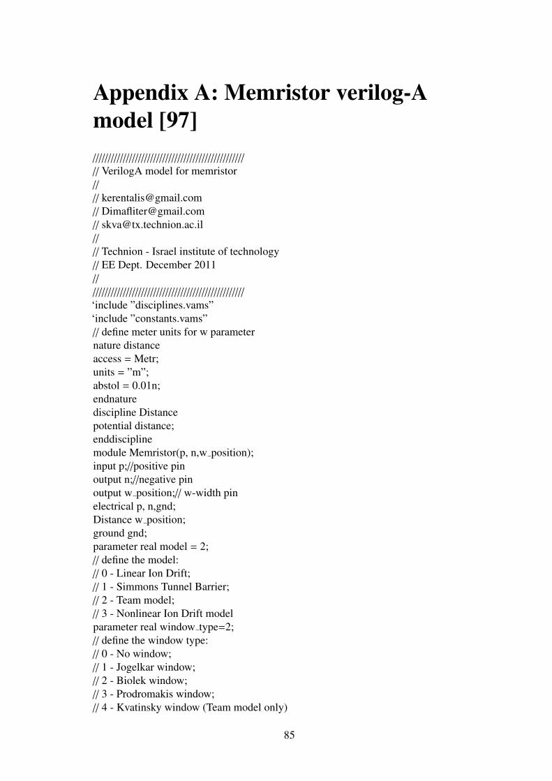
Appendix A: Memristor verilog-Amodel [97]//////////////////////////////////////////////////
// VerilogA model for memristor//
// [email protected]// [email protected]// [email protected]//
// Technion - Israel institute of technology// EE Dept. December 2011//
//////////////////////////////////////////////////
‘include ”disciplines.vams”‘include ”constants.vams”// define meter units for w parameternature distanceaccess = Metr;units = ”m”;abstol = 0.01n;endnaturediscipline Distancepotential distance;enddisciplinemodule Memristor(p, n,w position);input p;//positive pinoutput n;//negative pinoutput w position;// w-width pinelectrical p, n,gnd;Distance w position;ground gnd;parameter real model = 2;// define the model:// 0 - Linear Ion Drift;// 1 - Simmons Tunnel Barrier;// 2 - Team model;// 3 - Nonlinear Ion Drift modelparameter real window type=2;// define the window type:// 0 - No window;// 1 - Jogelkar window;// 2 - Biolek window;// 3 - Prodromakis window;// 4 - Kvatinsky window (Team model only)
85

parameter real dt=0;// user must specify dt same as max step size in// transient analysis & must be at least 3 orders//smaller than T period of the sourceparameter real init state=0.5;// the initial state condition [0:1]///////////// Linear Ion Drift model ///////////////
//parameters definitions and default valuesparameter real Roff = 200000;parameter real Ron = 100;parameter real D = 3n;parameter real uv = 1e-15;parameter real w multiplied = 1e8;// transformation factor for w/X width// in meter unitsparameter real p coeff = 2;// Windowing function coefficientparameter real J = 1;// for prodromakis Window functionparameter real p window noise=1e-18;// provoke the w width not to get stuck at// 0 or D with p windowparameter real threshhold voltage=0;// local variablesreal w;real dwdt;real w last;real R;real sign multply;real stp multply;real first iteration;////////// Simmons Tunnel Barrier model ///////////
//parameters definitions and default values//for Simmons Tunnel Barrier modelparameter real c off = 3.5e-6;parameter real c on = 40e-6;parameter real i off = 115e-6;parameter real i on = 8.9e-6;parameter real x c = 107e-12;parameter real b = 500e-6;parameter real a on = 2e-9;parameter real a off = 1.2e-9;// local variablesreal x;real dxdt;real x last;
86
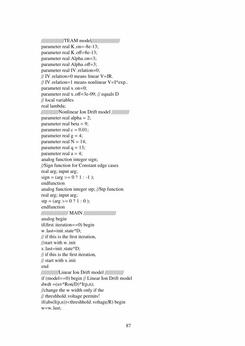
/////////////////TEAM model/////////////////////parameter real K on=-8e-13;parameter real K off=8e-13;parameter real Alpha on=3;parameter real Alpha off=3;parameter real IV relation=0;// IV relation=0 means linear V=IR.// IV relation=1 means nonlinear V=I*exp..parameter real x on=0;parameter real x off=3e-09; // equals D// local variablesreal lambda;/////////////Nonlinear Ion Drift model /////////////
parameter real alpha = 2;parameter real beta = 9;parameter real c = 0.01;parameter real g = 4;parameter real N = 14;parameter real q = 13;parameter real a = 4;analog function integer sign;//Sign function for Constant edge casesreal arg; input arg;sign = (arg >= 0 ? 1 : -1 );endfunctionanalog function integer stp; //Stp functionreal arg; input arg;stp = (arg >= 0 ? 1 : 0 );endfunction//////////////////// MAIN ////////////////////////
analog beginif(first iteration==0) beginw last=init state*D;// if this is the first iteration,//start with w initx last=init state*D;// if this is the first iteration,// start with x initend/////////////Linear Ion Drift model //////////////
if (model==0) begin // Linear Ion Drift modeldwdt =(uv*Ron/D)*I(p,n);//change the w width only if the// threshhold voltage permits!if(abs(I(p,n))<threshhold voltage/R) beginw=w last;
87
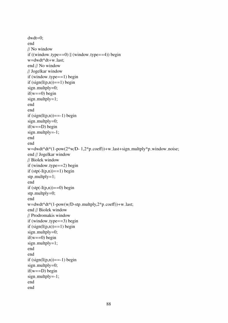
dwdt=0;end// No windowif ((window type==0) || (window type==4)) beginw=dwdt*dt+w last;end // No window// Jogelkar windowif (window type==1) beginif (sign(I(p,n))==1) beginsign multply=0;if(w==0) beginsign multply=1;endendif (sign(I(p,n))==-1) beginsign multply=0;if(w==D) beginsign multply=-1;endendw=dwdt*dt*(1-pow(2*w/D- 1,2*p coeff))+w last+sign multply*p window noise;end // Jogelkar window// Biolek windowif (window type==2) beginif (stp(-I(p,n))==1) beginstp multply=1;endif (stp(-I(p,n))==0) beginstp multply=0;endw=dwdt*dt*(1-pow(w/D-stp multply,2*p coeff))+w last;end // Biolek window// Prodromakis windowif (window type==3) beginif (sign(I(p,n))==1) beginsign multply=0;if(w==0) beginsign multply=1;endendif (sign(I(p,n))==-1) beginsign multply=0;if(w==D) beginsign multply=-1;endend
88

w=dwdt*dt*J*(1-pow(pow(w/D- 0.5,2)+0.75,p coeff))+w last+sign multply*p window noise;end // Prodromakis windowif (w>=D) beginw=D;dwdt=0;endif (w<=0) beginw=0;dwdt=0;end//update the output ports(pins)R=Ron*w/D+Roff*(1-w/D);w last=w;Metr(w position) <+ w*w multiplied;V(p,n) <+ (Ron*w/D+Roff*(1-w/D))*I(p,n);first iteration=1;end // end Linear Ion Drift model///////// Simmons Tunnel Barrier model ///////////
if (model==1) begin // Simmons Tunnel Barrier modelif (sign(I(p,n))==1) begindxdt =c off*sinh(I(p,n)/i off)*exp(- exp((x last-a off)/x c-abs(I(p,n)/b))-x last/x c);endif (sign(I(p,n))==-1) begindxdt =c on*sinh(I(p,n)/i on)*exp(-exp((a on-x last)/x c-abs(I(p,n)/b))-x last/x c);endx=x last+dt*dxdt;if (x>=D) beginx=D;dxdt=0;endif (x<=0) beginx=0;dxdt=0;end//update the output ports(pins)R=Ron*(1-x/D)+Roff*x/D;x last=x;Metr(w position) <+ x/D;V(p,n) <+ (Ron*(1-x/D)+Roff*x/D)*I(p,n);first iteration=1;end // end Simmons Tunnel Barrier model///////////////////// TEAM model //////////////////
if (model==2) begin // TEAM modelif (I(p,n) >= i off) begindxdt =K off*pow((I(p,n)/i off-1),Alpha off);end
89

if (I(p,n) <= i on) begindxdt =K on*pow((I(p,n)/i on-1),Alpha on);endif ((i on<I(p,n)) && (I(p,n)<i off)) begindxdt=0;end// No windowif (window type==0) beginx=x last+dt*dxdt;end // No window// Jogelkar windowif (window type==1) beginx=x last+dt*dxdt*(1-pow((2*x last/D- 1),(2*p coeff)));end // Jogelkar window// Biolek windowif (window type==2) beginif (stp(-I(p,n))==1) beginstp multply=1;endif (stp(-I(p,n))==0) beginstp multply=0;endx=x last+dt*dxdt*(1-pow((x last/D-stp multply),(2*p coeff)));end // Biolek window// Prodromakis windowif (window type==3) beginx=x last+dt*dxdt*J*(1- pow((pow((x last/D-0.5),2)+0.75),p coeff));end // Prodromakis window//Kvatinsky windowif (window type==4) beginif (I(p,n) >= 0) beginx=x last+dt*dxdt*exp(-exp((x last-a off)/x c));endif (I(p,n) < 0) beginx=x last+dt*dxdt*exp(-exp((a on-x last)/x c));endend // Kvatinsky windowif (x>=D) begindxdt=0;x=D;endif (x<=0) begindxdt=0;x=0;endlambda = ln(Roff/Ron);
90

//update the output ports(pins)x last=x;Metr(w position) <+ x/D;if (IV relation==1) beginV(p,n) <+ Ron*I(p,n)*exp(lambda*(x-x on)/(x off-x on));endelse if (IV relation==0) beginV(p,n) <+ (Roff*x/D+Ron*(1-x/D))*I(p,n);endfirst iteration=1;end // end Team model//////////// Nonlinear Ion Drift model ////////////
if (model==3) begin // Nonlinear Ion Drift modelif (first iteration==0) beginw last=init state;enddwdt = a*pow(V(p,n),q);// No windowif ((window type==0) —— (window type==4)) beginw=w last+dt*dwdt;end // No window// Jogelkar windowif (window type==1) beginw=w last+dt*dwdt*(1-pow((2*w last- 1),(2*p coeff)));end // Jogelkar window// Biolek windowif (window type==2) beginif (stp(-V(p,n))==1) beginstp multply=1;endif (stp(-V(p,n))==0) beginstp multply=0;endw=w last+dt*dwdt*(1-pow((w last-stp multply),(2*p coeff)));end // Biolek window// Prodromakis windowif (window type==3) beginw=w last+dt*dwdt*J*(1-pow((pow((w last- 0.5),2)+0.75),p coeff));end // Prodromakis windowif (w>=1) beginw=1;dwdt=0;endif (w<=0) beginw=0;dwdt=0;
91

end//change the w width only if the// threshhold voltage permits!if(abs(V(p,n))<threshhold voltage) beginw=w last;end//update the output ports(pins)w last=w;Metr(w position) <+ w;I(p,n) <+ pow(w,N)*beta*sinh(alpha*V(p,n))+c*(exp(g*V(p,n))- 1);first iteration=1;end // end Nonlinear Ion Drift modelend // end analogendmodule
92
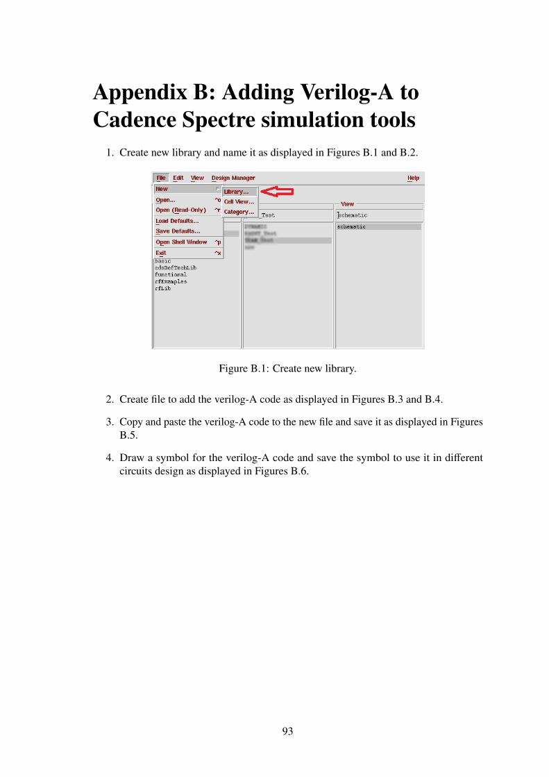
Appendix B: Adding Verilog-A toCadence Spectre simulation tools
1. Create new library and name it as displayed in Figures B.1 and B.2.
Figure B.1: Create new library.
2. Create file to add the verilog-A code as displayed in Figures B.3 and B.4.
3. Copy and paste the verilog-A code to the new file and save it as displayed in FiguresB.5.
4. Draw a symbol for the verilog-A code and save the symbol to use it in differentcircuits design as displayed in Figures B.6.
93
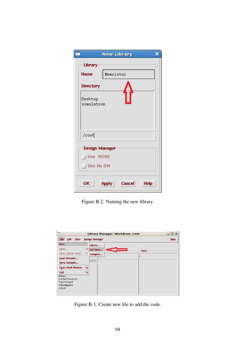
Figure B.2: Naming the new library.
Figure B.3: Create new file to add the code.
94
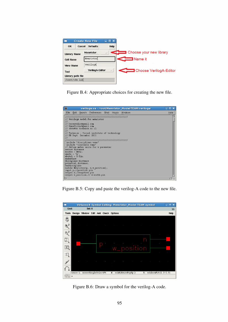
Figure B.4: Appropriate choices for creating the new file.
Figure B.5: Copy and paste the verilog-A code to the new file.
Figure B.6: Draw a symbol for the verilog-A code.
95

أ
ملخصال
يـــر قدرات تخـزيـنـــيـه ضخمـــة ـإنشـــاء تـقـنيــة ذاكـــرة شاملة ثابتة هو أمر حيـــوي البد منــه لتــوف عنــصــر الدائرة الرابـع "، (ممرستـــور) ةــاومــالمقذات رة ــالذاك. مطلوبـــة لوسائل الحوسبـــة النـانـويـــة
ديثــا هو المرشــح المــحتمــل لذاكـــرة الجيــل التــالي والتي أصبحــت محــل ، المكــتـشفــة ح"المـفقــــوديرجــع ذلــك االهتــمام بالــممرستـــور لمـمـــيزاتــه التــى . إهــتمــام بالــغ في السنــوات القــليـلــة اآلخيــرة
قـدرة , ـنولـوجيــا الــمســتخــدمــه حاليــاإستــهالك طـاقـه أقــل من الــتكـ, صغــر الــحجــم: تتــضمــنالــممرستــور علــى تغــييــر مقــاومتــه بنــاء علــى قيــمة الــتيــار الــمـار خـاللــه مع االحتــفــاظ بتــلك
في هـذا . ـورالــقيــمـه عنــد قطــع مصــدر الــتيــار بــاألضــافه إلــى قلــة تكــلفــة تصــنيــع الــممرستـالبحــث، تمــت مراجعــة اشكــال مخـتـلفـــه من التـقـنــيـــات المـــقتـــرحـــه لتــصنـيــع الممرستــور، كما تم
أيضـا، . إجــراء مقـــارنــة بيــن أفضــل تقـــنيــتيــن لتصـنيــع الممرستــور و الحصــول عليه كمنتـــج ماديالمخـتــلفــة المـعتــمـدة على الممرستــور مع أيضـاحهــا و بيــان افضــل تلــك تم ذكــر التـطبيـقــات
أحد اهــم تلـك التــطبــيقــات هو اســتخــدام الممرستــور كعــنصــر ذاكــره لتــخزيــن . التـــطبـيقــاتتبــر تطــبيــق يســتفــيــد بشــكــل مبــاشــر من أستــخــدام كعــنصــر ذاكــره لتــخزيــن البــيانــات يعــ. البــيانــات
األبحـــاث المـنشــــوره حاليـــا توضــح مشكـلة أستــخــدام الممرستــور كعــنصــر . ممــيــزات الممرستــور تــور و تـأثيــرتكــمن تلــك المــشكــلـــه فى عمــليــة قـــراءة البيــانــات المخــزنــه على الممرس. للــذاكـــرة
ه علــى البيــانــات المخــزنــه، حيـث انــه من الممـكــن تـدميــر البــيانــات المــخـزنــة علـى الــقراءعمــليــة يهــدف هـذا . الممرستــور خـالل عمــليــة القــراءة كمــا يظــهــر فـى تلــك االبحــاث الــمنــشــوره حــديثــا
تتــنــاول النــقطــه . ي األساس إلــى حــل هـذة المشكـلــة وذلــك مـن خــالل نقــطتــين رئيــسيــتيــــنالبــحـــث فعلى دوائــر /الكـتــابـــة من/األولــى اإلعــتــبـارات التى يجـــب مراعتــها عند تصمـيـــم دوائــر القـراءة
ـث تــم طــرح تلــك االعــتبــارات مع إيــضاح كيــفيــة االستــفاده حيـ. الذاكـــرة المـعتــمدة علـى الممرستــورو . منــها او تجــنب حــدوث مشــكــالت عنــد أستــخــدام الممرستــور كعــنصــر ذاكــره لتــخزيــن البــيانــات
كتــابـة جـديـــدة لحــل مشــكلــة /اءةمن ثـم، تـم استــخـدام تلــك االعتــبــارات فـى تصمـيــــم ثالث دوائـــــر قـر تـدميــر البــيانــات المــخــزنـــه علــى الممرستــور خــالل عمــليــة الـقــراءة باإلضافة إلى تســهيــل عمـليــة
عمــليــات بنــاءا علــى . القـراءة والكتـابــة من و إلى جهـــاز الممرستــور المسـتخــــدم كعـنصـــر للـذاكــــرةأظــهــرت دائــرتيــن , الــمحــاكــاه الــمعــتمــده علــى اخــر الــبيــانــات الــمنــشــورة حــديثــا عــن الممرستــور
مــن الثــالث دوائـــر الــمقــدمــه فــى هــذا الــبحــث قــدرتهــا علــى حــل تلــك الــمشــكلــه المتــعلــقه بتــدميــر

ب
كمــا تظــهر الدوائـــر المقــدمـــة . هــد أجــراء عمــليــة الــقــراءالــبيــانــات الــمخــزنــه علــى الــممــرستــور عن . الكـتــابـــة المنـشـــورة حـديثـــا/إستــهالك طاقـــة أقل و زمــن تأخيـــر أقـل مقــارنــة بدوائــر القــراءة
.، تشــغــل الدوائــر المقــدمـــة مسـاحـــة تصـميــــــم صغـــيــــرةباإلضافة إلى ذلك
:تــاليــهو تتكــون الرســاله من الفـصــول ال
(.ممــرستــور)االول يتــناول مقــدمــه عـن مــوضــوع الـبحــث الفصــل
التـكنــولــوجيــا الحــديثــه فــى مجــال الفصــل الثــانى يحــتوى علـى مســح عــام علــى ما تـوصلــت إلـيــه .الــرقمـيــه الــذاكــره
الفصــل الثــالــث بــه شــرح تـفــصيــلى لألنــواع الـمخــتـلفــه للــممــرستــور كمــا يقــدم مقــارنــه بيــن اشــهــر .نـوعيــن مـن تلــك االنــواع
كمــا يعــرض مســح . تعــتمــد علــى الـممــرستــورطبيــقات المخــتلــفه الـتــى الفصــل الــرابــع ينــاقــش الــتعلــى الــذاكــره الـمعــتمــده علــى /مـن لكــتابــها/عــام علــى االوراق البـحثـيــه التــى تعــرض دوائــر القــراءهشـرح مبــسط ألهـم التـقنــيـات و األسـاليــب الـممــرستــور كعــنصــر ذاكــره لحــفـظ البــيانــات مع
.مع ايــضاح ما تواجهــه تلــك الــدوائــر مـن مــشكــالت المــستـخــدمــه
علــى الــذاكــره الـمعــتمــده علــى الـممــرستــور /مـن الكــتابــه/القــراءه جــديـده الفصــل الخــامس يقــدم دوائــرالـمحــاكــاه الـخــاصــه بـالـدوائــر كمــا يقــدم مقــارنــه بيــن نتــائــج. ــنصــر ذاكــره لحــفـظ البــيانــاتكع
.الـمقــتـرحـه فـى الـرســالـه و نتــائــج الـمحــاكــاه للـدوائــر الـســابقــه
كمــا . ـه و المعــروضــه في الرسـالهو هو ملخــص ألهــم الوسائــل المسـتخـدمـالفصــل الـســادس يحــتــوى عــرض ألهــم النتـائـج التي تحتـويهــا الرسـالــه و كــذلــك عــرض األبـحــاث المــنشــوره و أهــم
.األضـافــات و الخـطــط المســتقــبلـيــه الستكـمــال العمـل

محمــد سيــد أحمــد محمــد الشــامى :دسـمهن 2891\3\12 :تاريخ الميالد
مصــرى :الجنسية 1121\21\21 :تاريخ التسجيل
..........\....\.... :تاريخ المنح ةت و االتصـــــاالت الكـهـــربــيـــــلـكتــرونيـااال :القسم ماجستير :الدرجة
:المشرفون محمــد ســامــح سعـــيد. د.ا حســن مصــطفــى حســن. د :لممتحنونا (الممتحن الخارجي) حســنيــن عـامــر حـامــد. د.أ (الممتحن الداخلي) محمــد فـتــحــى. د.أ (المشرف الرئيسي) محمــد ســامــح سعـــيد. د.أ
:عنوان الرسالةه ذات ــاومـده على المقـــتمـره المعــذاكـات الــوفــفـمص بــرمجـــةه لــــاسبـمن ةـــربائيـر كهـم دوائــتصمي .(ورــرستـمم)ره ـــالذاك
:الكلمات الدالة كـتابــه/ممــرستــور، دائـرة، قراءه، الـذاكره النــانو
:رسالةملخـص ال
، و المعروفه بالعنصر المفقود الرابع، تعتبر مرشح محتمل (ممرستور)المقاومه ذات الذاكره القى الممرستور اهتمام كبير من المجتمع البحثى خالل السنين القليله . للجيل القادم من الذاكره
تقدم تلك الرساله ثالث دوائر مناسبه لالستخدام فى مصفوفات الذاكره المعتمده على . الماضيهأوال، دائرتين من الثالث دوائر . الكتابه المقدمه بثالث ميزات اساسيه/تتميز دوائر القراءه. الممرستور
تعتبر تلك الميزه هى االهم لما . ه تمتاز بميزة القراءه دون التأثير على المعلومات المخزنهالمقدمثانيا، . تعانيه الدوائر المقترحه حاليا من مشكلة تدمير البيانات المخزنه على الممرستور عند قرائتها
خيرا، الدوائر المقدمه و أ. اــالدوائر المقدمه تشغل مساحه صغيره مقارنة بما تم نشره من دوائر مسبقعلى /كتابه من/اقل استهالكا للطاقة و لها زمن تأخير أقل مقارنة بأخر ما تم نشره من دوائر قراءه
. الممرستور

رهــذاكـاتالــوفــفـمصبــرمجـــةهلــــاسبـمنةـــربائيـركهـمدوائــتصمي
(ورــرستـمم)رهـــهذاتالذاكــاومـدهعلىالمقـــتمـالمع
اعداد
محمــدسيــدأحمــدمحمــدالشــامى
القاهرةجامعة-الهندسةكليةإلىمقدمةرسالة
العلومماجستيردرجةعلىالحصولمتطلباتمنكجزء
في
واالتصـــــاالتالكـهـــربـيـــــةلـكتــرونيـاتاال
:يعتمدمنلجنةالممتحنين
مــدسامــحسعــيدالمشرفالرئيسىمح:االستاذالدكتور
خليادالممتحنالمحمـدفـتحــى:االستاذالدكتور
حسـنيـنعامـرحامـدالممتحنالخارجي:االستاذالدكتور
ربيةـتصاالتالكهتواالالكترونياذااللكترونياتبقسماالأست
األمريكيهبالقاهرةالجامعة-دسةالهنكلية
القاهــرةجامعــة-الهندســةكليــة
العربيــةمصـرجمهوريـة-الجيـزة
4102

رهــذاكـاتالــوفــفـمصبــرمجـــةهلــــاسبـمنةـــربائيـركهـمدوائــتصمي
(ورــرستـمم)رهـــهذاتالذاكــاومـدهعلىالمقـــتمـالمع
داعدا
محمــدسيــدأحمــدمحمــدالشــامى
القاهرةجامعة-الهندسةكليةإلىمقدمةرسالة
العلومماجستيردرجةعلىالحصولمتطلباتمنكجزء
في
واالتصـــــاالتالكـهـــربـيـــــةلـكتــرونيـاتاال
تحتاشراف
حســنمصـطفــىحســن.د
……………………....
مــحسعـيــدمحمــدسا.د.أ
……………………....
توالكترونيااللكترونياتبقسماال درسم
ربيــةـتصاالتالكهاال
القاهرةجامعة-الهندسةكلية
توالكترونياذااللكترونياتبقسماالأست
ربيــةـتصاالتالكهاال
القاهرةجامعة-الهندسةكلية
القاهــرةجامعــة-الهندســةكليــة
العربيــةمصـرجمهوريـة-زةالجيـ
4102

رهــذاكـاتالــوفــفـمصبــرمجـــةهلــــاسبـمنةـــربائيـركهـمدوائــتصمي
(ورــرستـمم)رهـــهذاتالذاكــاومـدهعلىالمقـــتمـالمع
اعداد
محمــدسيــدأحمــدمحمــدالشــامى
القاهرةجامعة-الهندسةكليةإلىمقدمةرسالة
العلومماجستيردرجةعلىالحصولمتطلباتمنكجزء
في
واالتصـــــاالتالكـهـــربـيـــــةلـكتــرونيـاتاال
القاهــرةجامعــة-الهندســةكليــة
العربيــةمصـرجمهوريـة-الجيـزة
4102