Embed Size (px)
Citation preview
Substrate Integrated Waveguide Circuits
and Systems
Nathan Alexander Smith
Department of Electrical & Computer Engineering McGill University
Montréal, Québec, Canada
May 2010
A thesis submitted to McGill University in partial fulfillment of the requirements for the degree of Master of Engineering.
© 2010 Nathan Alexander Smith

i
Abstract
This thesis investigates substrate integrated waveguide (SIW) based interconnects,
components, and systems. SIWs are high performance broadband interconnects with
excellent immunity to electromagnetic interference and suitable for use in microwave and
millimetre-wave electronics, as well as wideband systems. They are very low-cost in
comparison to the classic milled metallic waveguides as they may be developed using
inexpensive printed circuit board (PCB) fabrication techniques. In this thesis, the
interconnect design is studied by investigating the modes supported by SIW using
fullwave simulations. Also, SIW transitions, as well as miniaturization methods to
decrease the waveguide footprint are evaluated. Next, a miniaturized Wilkinson SIW
power divider is developed exhibiting excellent isolation of up to 40dB between its
output ports. Another SIW component investigated in this thesis is an SIW cavity
resonator. A circular SIW cavity resonator fed by a microstrip line and via probe through
an opening on the top cavity wall is designed. The aperture on the top wall creates a
radiating folded slot and measurements show a gain of 7.76dB for this cavity-backed
antenna at 16.79GHz. The antenna exhibits a bandwidth of 250MHz (return loss > 10dB).
With this resonator, a microwave oscillator is designed to produce a 10dBm tone.
Measurements of the fabricated oscillator demonstrate a low phase noise of -82dBc/Hz.
Finally, a new SIW component, i.e. tapered SIW reflector, is designed to counteract the
dispersive behavior of an SIW interconnect near cutoff. Two dispersion equalization
systems are implemented using either a circulator or a coupler to route the compensated
reflected signal. The systems are tested when a 1Gbps pseudo-random binary signal is
up-converted to 10.7GHz and launched into the SIW interconnect. Observation of the

ii compensated output eye-diagrams reveals achievement of a lower distortion in the highly
dispersive band just above the cutoff frequency.

iii
Abrégé
Cette thèse examine des interconnexions, des composantes et des systèmes basés sur des
guides d’ondes intégrés au substrat (GIS). Les GIS sont des interconnexions de haute
performance à large bande qui possèdent d’excellentes caractéristiques d’immunité
contre les interférences électromagnétiques et qu’on pourrait utiliser dans des systèmes
microondes et des circuits d’ondes millimétriques. Le coût des GIS est très faible
comparativement à celui des guides d’ondes métalliques communs, car leur fabrication
utilise des techniques peu coûteuses de production de cartes de circuits imprimés. Cette
thèse étudie, au moyen de simulations à onde entière, le design de l’interconnexion et les
modes supportés par le GIS. De plus, la thèse évalue les transitions des GIS ainsi que les
méthodes de miniaturisation visant à diminuer l’empreinte du guide d’onde. Ensuite, la
thèse expose le développement d’un répartiteur de puissance GIS Wilkinson qui possède
d’excellentes propriétés isolantes allant jusqu’à 40dB entre les bornes de sortie. La thèse
examine aussi une autre composante GIS: un résonateur à cavité GIS. La thèse décrit la
conception d’un résonateur à cavité GIS qui est alimenté par une ligne microbande et une
sonde passées par une aperture sur le mur supérieur de la cavité. L’aperture dans le mur
supérieur crée une encoche plissée rayonnante, et des mesures ont révélé un gain de
7,76dB pour l’antenne adossée d’une cavité de 16,79 GHz. L’antenne possède une bande
passante de 250MHz (perte de réflexion > 10dB). En plus de ce résonateur, un oscillateur
micro-onde est conçu pour produire une tonalité de 10dBm. Les mesures de l’oscillateur
fabriqué montrent un faible bruit de phase de -82dBc/Hz. Enfin, une nouvelle
composante de GIS (un réflecteur effilé) est conçue pour compenser la caractéristique
dispersive d’une interconnexion GIS près de la fréquence de coupure. Deux systèmes de

iv correction de la dispersion sont appliqués à l’aide d’un circulateur ou d’un coupleur qui
dirige le signal réfléchi corrigé. Ces systèmes sont testés par signal binaire pseudo-
aléatoire de 1Gbps, converti à 10,7GHz et lancé dans l’interconnexion GIS.
L’observation, à la sortie, des diagrammes de l’œil révèle une plus faible distorsion dans
la bande hautement dispersive, immédiatement au-dessus de la fréquence de coupure.

v
Acknowledgments
To begin, I must thank my mother for her unconditional love and for always
believing in me. I would like to thank my grandmother for stressing the value of
education and for her support in my continuing studies. I would like to thank my father
for providing me with a place to stay in Montreal and all the wonderful getaways out of
the city.
I would like to thank my supervising professor, Dr. Ramesh Abhari, for providing
me with this wonderful opportunity to study with the Integrated Microsystems
Laboratory at McGill University. I am very grateful for your guidance and support. I
value the experience I have acquired tremendously. The Interconnects and Signal
Integrity course developed by Dr. Abhari provides excellent insight into the challenges of
high-frequency signaling and system design. I particularly enjoyed this class, as well as
the Analog Microelectronics, and Radio Frequency Microelectronics courses taught by
Professor Gordon Roberts, and Frederic Nabki (filling in for Dr. Mourad El-Gamal),
respectively. I feel as though I have been able to focus my efforts on design and this
thesis presents several new microwave circuit and system designs. I could not have
completed this work without the hard work of my Professors and their dedication to their
work.
I would like to thank my colleagues Asanee Suntives (Ph.D.), Kasra Payandehjoo
(Ph.D. candidate), and Darryl Kostka (MEng) for all of their support and help with the
simulation software. Again, I could not have completed this work without all of your hard
work, dedication, and excellence.

vi
I would like to thank David Lee of Communications Research Center Canada for
providing the anechoic chamber measurement data for the resonators presented in this
thesis.
Finally, I would like to thank Bob Thomson and Don Pavlasek for their help
assembling my prototypes. Mr. Thomson is a wealth of information and I value our
friendship very much. Thank you for taking the time to answer my never-ending
bombardment of questions.

vii
Contents
1 Introduction ................................................................................................................... 1
1.1 Overview ................................................................................................................ 1
1.2 Thesis Motivations and Objectives ....................................................................... 3
1.3 Thesis Contributions and Publications..………………………………….………5
1.4 Thesis Outline ........................................................................................................ 8
2 Substrate Integrated Waveguide Interconnects ..................................................... 10
2.1 Substrate Integrated Waveguide Technology .................................................... 10
2.1.1 Introduction……………………………………………………………..10
2.1.2 Implementation………………………………………………………….11
2.1.3 Surface Currents and Supported Modes………………………………...17
2.2 Substrate Integrated Waveguide Transitions ..................................................... 25
2.3 Reducing the Footprint of Substrate Integrated Waveguides ............................ 28
2.4 Summary ............................................................................................................ 32
3 Substrate Integrated Waveguide-Based Components .......................................... 33
3.1 Introduction…………………………………………………………………..33
3.2 SIW Filters and Cavity Resonators………………………………………….34
3.2.1 SIW Cavity Resonators………………………………………………..35
3.2.2 SIW Bandpass Filters………………………………………………….37

viii
3.2.3 Evanescent Mode Filters………………………………………………38
3.2.4 All-pass Filters…………....…………………………………………...39
3.3 SIW Directional Couplers and Hybrid Junctions ............................................. 40
3.4 Applications of SIW Components in Electronic Circuits and Systems............ 46
3.5 Summary ........................................................................................................... 50
4 Substrate Integrated Waveguide Power Dividers……………………………….51
4.1 Survey of Existing Power Divider Technology ................................................. 51
4.1.1 Introduction to Power Dividers..………………………………………51
4.1.2 Implementation: Waveguide and SIW Power Dividers………………..53
4.1.3 Implementation: Microstrip and Stripline Wilkinson Power Dividers...55
4.2 Compact SIW Power Dividers .......................................................................... 60
4.2.1 Compact Folded SIW Power Dividers…………………………………61
4.2.2 Compact Half-Mode SIW Wilkinson Power Dividers…………………66
4.3 Summary……...……………………………………………………………….74
5 Substrate Integrated Waveguide Cavity Resonators and Antennas……………76
5.1 SIW Cavity Resonators, Antennas, and Oscillators .......................................... 76
5.1.1 Introduction……………………………………………………………..76
5.1.2 SIW Cavity Resonator Oscillators………………………………………77
5.1.3 SIW Cavity Resonator Antennas………………………………………..78
5.2 Microstrip-Fed Circular SIW Cavity Resonators and Antennas ....................... 79

ix
5.2.1 Design and Measurement of Microstrip-Fed Circular SIW Cavity
Resonators………………………………………………………………79
5.2.2 A Series Feedback pHEMT Microstrip-Fed Circular SIW Cavity Resonator
Oscillator………………………………………………………………...91
5.3 Summary .......................................................................................................... 101
6 Dispersion Equalization Techniques for Substrate Integrated Waveguide
Interconnects…………………………………………………………………103
6.1 Waveguide Dispersion Equalization Techniques ............................................ 103
6.1.1 Introduction…………………………………………………………….103
6.1.2 Dispersion in Waveguides……………………………………………...104
6.1.3 Dispersion Equalization Systems with All-pass Networks……………..105
6.1.4 Linearly Tapered Dispersion Equalizer………………………………...107
6.2 SIW Dispersion Compensation System Design .............................................. 110
6.2.1 Designing the Tapered SIW Equalizer………………………………….111
6.2.2 Characterizing the Designed Reflective Equalizer Component………...113
6.2.3 Dispersion Equalization System Implementation……………………….117
6.3 Time Domain Evaluation................................................................................. 122
6.4 Summary .......................................................................................................... 124
7 Conclusions…………………………………………………………………...126
7.1 Thesis Summary and Conclusions……………………………………………126

x
7.2 Future Work Recommendations ......................................................................... 128
References ....................................................................................................................... 130

xi
List of Figures 2.1 The geometry of the SIW. Substrate thickness: h, waveguide physical width: w, via
spacing: s, via diameter: d........................................................................................... 12
2.2 TE10 surface current distribution on a RWG with narrow slots opening the sides. .... 12
2.3 TEm0 modes propagating in the z-direction. ............................................................... 15
2.4 Angle of incidence of electromagnetic waves bouncing off metalized vias affects
ultimate leakage. ......................................................................................................... 16
2.5 Magnitude of electric field for (a) TE10, (b) TE20, (c) TE11 , and (d) TM11 , on the
broadside wall of the rectangular waveguide, at 110GHz. ......................................... 18
2.6 Magnitude of electric field for (a) TE10, (b) TE20, (c) TE11, and (d) TM11, at the
cross-section of the rectangular waveguide, at 110GHz. ............................................ 18
2.7 Surface current vectors along a sidewall of a rectangular waveguide for (a) TE10, (b)
TE20, (c) TE01, (d) TE11, and (e) TM11, at 110GHz .............................................. 20-21
2.8 Slotted sidewall rectangular waveguide (a) Structure, (b) Magnitude of electric field
for TE10 at 110GHz..................................................................................................... 22
2.9 Magnitude of electric field for (a) TE01, and (b) TM11 at 110GHz............................. 22
2.10 Laminated waveguide with 3 “sub-conductor” layers. ............................................. 23
2.11 Cross-sectional magnitude of electric field for (a) TE10 and (b) TM11. at 115GHz. . 24
2.12 Laminated waveguide side-wall surface current vectors for (a) TE10 and (b) TM11 24
2.13 Laminated waveguide is shown to support TM11 with no leakage at 115GHz. ....... 24
2.14 The E field distribution at the (a) input and (b) output, of a microstrip to SIW
transition. At the output, the field distribution is observed to resemble TE10 in SIW. 26

xii 2.15 The TE10 mode electric field lines are folded under a conductor ledge in the folded
SIW geometry. .......................................................................................................... 29
2.16 HMSIW interconnect. ............................................................................................... 31
2.17 FHMSIW (T-Septum) interconnect. ......................................................................... 32
3.1 Magnitude of electric field distribution in an SIW cavity for TE101 (a) at 10GHz, and
(b) at resonance frequency 8.1241GHz , simulated in HFSS. .................................... 36
3.2 Fabricated SIW Riblet short-slot 3dB coupler (a) layout, (b) photograph. ................ 42
3.3 Simulated and measured (a) S21, S31, (b) S11, S41, (c) S22, S33, S44, (d) phase difference
for the fabricated SIW Riblet short-slot coupler................................................... 43-44
3.4 Stripline to TE20 excited SIW balun. .......................................................................... 49
4.1 SIW three-port power divider (a) Y-junction, (b) T-junction..................................... 53
4.2 SIW three-port power divider Y-junction, (a) excitation at port 1 (b) excitation at
ports 2, or 3. ................................................................................................................ 54
4.3 Transmission line model of a lossless T-junction....................................................... 54
4.4 Wilkinson power divider transmission line model. .................................................... 56
4.5 Normalized and symmetric Wilkinson power divider circuit..................................... 56
4.6 Even-mode analysis circuit for the Wilkinson power divider. ................................ ... 57
4.7 Odd-mode equivalent circuit for the Wilkinson power divider. ................................. 58
4.8 S-parameters for 10GHz Wilkinson lossless transmission line power divider. .......... 60
4.9 Proposed folded SIW power divider prototype signal conductor geometry with
stripline inputs and outputs. ........................................................................................ 61
4.10 Cross-sectional electric field line distribution in proposed folded SIW power
divider. ........................................................................................................................ 62

xiii 4.11 Microstrip to stripline vertical transition implemented in the prototype for testing of
the folded SIW power divider. ................................................................................. 62
4.12 Simulated structure for the folded SIW power divider including microstrip to
stripline transitions and SMA connectors................................................................. 64
4.13 Simulated S-parameters for the proposed folded SIW power divider. ..................... 64
4.14 Measured S-parameters for the folded SIW power divider prototype. ..................... 65
4.15 Reviewed HMSIW Wilkinson power divider........................................................... 66
4.16 Simulated (a) S21, S31, S32, (b) S11, S22, S33 for reviewed HMSIW Wilkinson power
divider....................................................................................................................... 67
4.17 Magnitude of the electric field in the all waveguide half-mode SIW power divider:
(a) Excitation of Port 1, (b) Excitation of port 2 or 3 (port 3 shown, 10.5GHz). .. 68
4.18 Magnitude of simulated S11, S21, S31, and S32. ........................................................... 69
4.19 Proposed HMSIW Wilkinson power divider prototype, at 10.5GHz. ...................... 70
4.20 Simulated and measured (a) S21, S31, S32, (b) S11 and (c) S22 for the HMSIW
Wilkinson power divider. ................................................................................... 71-72
4.21 Fabricated HMSIW Wilkinson power divider prototype.......................................... 73
5.1 Layout of the proposed microstrip-fed circular SIW cavity resonator. ...................... 81
5.2 Simulated return loss for the proposed resonator. ...................................................... 81
5.3 Photograph of the fabricated SIW circular cavity resonators. .................................... 82
5.4 (a), (b) Measured return loss for two fabricated samples of the resonator. ................ 83
5.5 Simulated input impedance magnitude of the designed SIW resonator. .................... 84
5.6 The equivalent RLC circuit of the resonator model with feed line. ............................ 85

xiv 5.7 Simulated input reflection coefficient, or S11, locus of the resonator with R = ± jX
arcs .............................................................................................................................. 86
5.8 Simulated input reflection coefficient, or S11, locus of the RLC equivalent circuit with
R = ± jX arcs................................................................................................................ 87
5.9 Measured input reflection coefficient, or S11, locus of the fabricated resonator with R
= ± jX arcs ................................................................................................................... 87
5.10 Measured resonator input impedance magnitude ..................................................... 88
5.11 3-D radiation pattern for the proposed resonator antenna ........................................ 89
5.12 Simulated (16.13GHz) and measured (16.79GHz) xz-plane radiation pattern for
SIW cavity-backed antenna ........................................................................................ 90
5.13 Simulated (16.13GHz) and measured (16.79GHz) yz-plane radiation pattern for
SIW cavity-backed antenna ........................................................................................ 90
5.14 Schematic of the proposed series feedback reflection oscillator. The matching
network is denoted as MN, the low-pass filter is denoted as LPF............................ 91
5.15 Series reflection oscillator PCB layout. .................................................................... 93
5.16 ADS schematic for the series reflection oscillator.................................................... 94
5.17 Simulated output spectrum and time domain waveform for the series reflection
oscillator. .................................................................................................................. 95
5.18 Photograph of the fabricated microwave oscillator. ................................................ 95
5.19 Measured output spectrum for the fabricated oscillator (a) Span = 50MHz, (b) Span
= 500kHz................................................................................................................ 96

xv 5.20 Radial stub performance test circuits for modeling transmission from source to load
in presence of shunt RF choke including wire and the DC supply: (a) Original RF
choke design, (b) Improved RF choke design. ......................................................... 98
5.21 Radial stub S-parameters for the test circuit of Figure 5.20 (a) with the stub length =
3.49mm..................................................................................................................... 98
5.22 Radial stub S-parameters for the test circuit of Figure 5.20 (b) with two stubs each
with the length = 8.815mm....................................................................................... 99
5.23 Second reflection oscillator layout.......................................................................... 100
5.24 ADS harmonic balance simulation results for second oscillator design................. 101
6.1 Dispersion diagram of a typical SIW........................................................................ 105
6.2 Circulator-based all-pass waveguide dispersion equalizer. ...................................... 106
6.3 3dB coupler-based waveguide dispersion equalizer. ................................................ 107
6.4 Linearly tapered waveguide dispersion equalizer..................................................... 107
6.5 SIW with microstrip transitions (not to scale). ......................................................... 110
6.6 Equalizer time delay as a function of linear taper constant, a. ................................. 111
6.7 Total equalized time delay as a function of linear taper constant, a. ........................ 112
6.8 Tapered waveguide equalizer (not to scale). ............................................................. 114
6.9 Simulated and measured results of the uniform SIW with microstrip launchers: (a)
Magnitude of S-Parameters, (b) Continuous phase of S21. ....................................... 115
6.10 Simulated and measured results of the linearly tapered SIW with a microstrip
launcher: (a) Magnitude of S11, (b) Continuous phase of S21. ................................ 116
6.11 Fabricated circulator-based equalization system. ................................................... 117
6.12 Fabricated coupler-based equalization system. ....................................................... 117
xvi 6.13 (a) Simulated and measured S-parameters for circulator-based dispersion
equalization system, (b) Measured S-parameter data for coupler-based dispersion
equalization system........................................................................................... 118-119
6.14 Simulated and Measured continuous phase for circulator and coupler-based
dispersion equalization systems as well as the calculated phase for the input SIW. 120
6.15 Simulated group delay plot for both dispersion equalization systems. ................... 121
6.16 Measured group delay approximation for both dispersion equalization systems. .. 122
6.17 Block diagram for dispersion compensating SIW high-speed pulse transmission
system……………………………………………………………………………. 123
6.18 Measured eye diagrams with a 10.7GHz carrier at the output of (a) the un-equalized
SIW interconnect, (b) circulator-based equalized system, and (c) coupler-based
equalized system. ............................................................................................ 123-124

xvii
List of Tables 2.1 Cutoff Frequencies of Higher Order Modes Found Analytically ............................... 17

xviii
List of Acronyms
1-D One-Dimensional 2-D Two-Dimensional
3-D Three-Dimensional ADS Advanced Design System AC Alternating Current APS Antenna and Propagation Society Symposium CAD Computer Aided Design CBCPW Conductor Backed Coplanar Waveguide CPW Coplanar Waveguide DC Direct Current EBG Electromagnetic Band Gap
EMI Electromagnetic Interference GaAs Gallium Arsenide HFSS High Frequency Structure Simulator HMSIW Half-Mode Substrate Integrated Waveguide HR-Si High-Resistivity Silicon IEEE Institute of Electrical and Electronics Engineers IF Intermediate Frequency IMEC Interuniversity Microelectronics Center IMS International Microwave Symposium IPD Integrated Passive Device LTCC Low Temperature Co-fired Ceramic
MCM Multi-Chip Module MCM-D Multi-Chip Module-Deposited MMIC Monolithic Microwave Integrated Circuit PCB Printed Circuit Board pHEMT Pseudomorphic High Electron Mobility Transistor PLL Phase Locked Loop RF Radio Frequency RBW Resolution Bandwidth RWG Rectangular Waveguide SIFW Substrate Integrated Folded Waveguide SIW Substrate Integrated Waveguide SoS System-on-Substrate TE Transverse Electric TEM Transverse Electromagnetic TM Transverse Magnetic
UWB Ultra-Wideband VCO Voltage Controlled Oscillator

xix
VNA Vector Network Analyzer WLAN Wireless Local Area Network WPAN Wireless Personal Area Network

1
Chapter 1 Introduction 1.1 Overview
In the last decade, a tremendous amount of research has been carried out to develop
high-performance microwave and millimeter-wave waveguide components that are
fabricated using low-cost technologies. Among these are the substrate integrated
waveguides (SIWs), initially introduced as laminated waveguides [1, 2], that can be
easily implemented using common printed circuit board (PCB) fabrication methods.
Since the introduction of SIWs, or laminated waveguides, various SIW-based
components, interconnects, and circuits have been developed and their advantages are
justified in comparison to their milled waveguide or transmission line based counterparts.
As interconnects, it is seen that the substrate integrated waveguide (SIW) interconnects
provide a broadband bandpass signaling medium with excellent isolation of
electromagnetic interference (EMI) [3], while planar conventional transmission lines are
known as the performance bottleneck in ultra wideband systems due to their limited
bandwidth and high-frequency losses. In an SIW, the electric field distribution fills the
volume inside the waveguide interconnect and surface currents propagate on the larger
total cross-sectional area of the waveguide walls, resulting in lower conductor losses [4].
As clock frequencies and circuit densities continue to increase, closely spaced microstrip
and stripline interconnects will no longer be viable options for interconnection of system
modules due to their open structure and increased susceptibility to crosstalk and EMI.

1.1 Overview 2 The demands for wideband interconnects and compact electronic systems are
continuously increasing. This necessitates employing the SIW technology in future ultra-
high frequency and broadband applications and highly integrated systems.
SIW is a 3-dimensional (3-D) structure for signal transmission and its integration with
planar circuits, lines, and connecting pads may seem challenging. A host of mode and
impedance matching transitions from SIW to microstrip, stripline, coplanar waveguide
(CPW), and conductor backed coplanar waveguide (CBCPW) have been developed to
address this concern [4-10]. These transitions, like the SIW, are all implemented using
the same fabrication process as the rest of system’s layout.
SIWs, as a new means of signal transmission, have been the basis for the design of
many circuit components. Components such as power dividers, resonator cavities, and
filters that have been developed using microstrip, stripline or milled-waveguide
technologies are now redesigned using the SIW platform. The criticism that has been
raised about these new interconnects and components is that they possess a relatively
large footprint. Research works published in [7], [11-14] have in particular focused on
the development of waveguide miniaturization methods.
Various types of SIW power dividers, couplers, and diplexers have been designed and
optimized for operation at microwave and mm-wave frequency bands using PCB
substrates [15-23]. Other SIW-based components like waveguide cavities have also been
integrated directly into a PCB platform, allowing significant cost reduction in the
development and mass production of resonator based microwave oscillators and filters.
The high quality factor of the waveguide cavities provides excellent frequency selectivity
for cavity coupled filters and resonators [24-26]. The frequency selectivity of coupled

1.1 Overview 3 SIW cavities is exploited in numerous microwave filter topologies [27-30]. It is now
possible to develop fully integrated multichip module (MCM) systems incorporating SIW
filters and high-gain antennas. Slot array SIW antennas and SIW cavity-backed antennas
provide microwave system designers with the ability to incorporate low cost, high-
performance antennas on the same substrate as monolithic microwave integrated circuits
(MMIC) [26], [31-33].
One of the most attractive applications of the SIW technology is in space exploration.
With the passing of the 40-year anniversary of the Moon landing, much international
interest exists in further space exploration, including missions to Mars. Due to the
astronomical travel distances of such missions, payload reduction is critical in
maximizing fuel efficiency. The development of ultra-light SIW-based electronic
communication systems will decrease overall spacecraft and satellite payloads in
comparison to units deployed with milled metallic waveguides [34]. Lightweight SIW
antenna arrays will be critical in developing portable communication base stations for
space exploration systems. In addition, the SIW components are excellent candidates for
application in Earth orbiting satellites, un-manned drone aircraft, ground-to-air base
stations, as well as internet and high-speed data hubs, among others.
1.2 Thesis Motivations and Objectives
The development of the SIW-based components marks a revolutionary period in the
design of all-electrical microwave and millimeter-wave electronics. As system clock
frequencies and integration densities continue to increase, the use of the SIW
interconnects in high performance communication electronics should become very

1.2 Thesis Motivations and Objectives 4 commonplace. It has been reported in literature that due to the high EMI isolation
provided by the closed waveguide structures, the SIW can eliminate cross-talk in
sensitive microwave and mm-wave circuits. Also, researchers have demonstrated that low
conductor losses and higher power handling in the SIW interconnects provide enhanced
signaling performance in comparison to other PCB transmission lines. Since SIWs are
dispersive interconnects, in wideband applications, in order to achieve a maximum
distortion-free link bandwidth, dispersion equalization techniques should be employed.
This has not been done in any of the previously published results, to best of the author’s
knowledge. Dispersion equalization can be implemented at the baseband in the driver or
receiver stages of an SIW interconnect or at the RF level integrated with the SIW
interconnect. Implementation of the latter methods is one of the objectives of this thesis.
The goal is to develop reflection based dispersion equalization systems to maximize the
SIW interconnect’s operating bandwidth. Before implementing this goal, it is intended in
this thesis to first study and design SIW interconnects and a few important SIW
components such as power dividers and cavity resonators.
In order to route signals in SIW-based systems, compact SIW power dividers are
required. The designs presented so far in literature follow the objectives of size reduction
and achieving wide operational bandwidth. In this thesis, it is aimed to develop compact
SIW power dividers with good isolation between output ports, as required in many
microwave systems.
Another objective of this thesis is to investigate a sample of SIW-based cavity
resonators that can be used in antenna or oscillator circuit designs. As mm-wave
frequencies are becoming further exploited for consumer applications, such as
1.2 Thesis Motivations and Objectives 5 automotive radar or personal area networks, SIW antennas and resonators become more
attractive candidate components for circuit design. In this thesis, to simplify the design
and test process, an SIW cavity is developed for operation in the Ku band.
The relatively low-cost high-performance SIW systems will undoubtedly find
application in future microwave and mm-wave engineering projects. New SIW
components are emerging and this thesis focuses on a few designs, to the extent possible,
within the scope of a master’s thesis.
1.3 Thesis Contributions and Publications
This thesis presents the reader with a comprehensive overview of the SIW research
conducted during the period from 1998-2009. Following an in depth analysis of the
previously published SIW research, all-new SIW-based components and systems are
developed in this thesis. Namely, three components, i.e. SIW power divider, SIW cavity,
and SIW taper, are designed and fabricated for experimental evaluations. The objective
for the SIW power divider design is to decrease the overall dimensions of the unit and
simultaneously provide improved isolation performance between the two output ports. A
miniaturized Wilkinson SIW power divider is developed. The fabricated design achieves
up to 40dB of isolation between output ports, in comparison with approximately 7dB of
isolation provided by the previously available SIW power divider configuration presented
in [22] while a width reduction of nearly one half is also achieved.
An all-new microstrip-fed circular SIW cavity resonator is designed and fabricated.
Vector network analyzer (VNA) and anechoic chamber measurements are recorded for
the new resonator structure. These results demonstrate a Q factor of 76.3 and a bandwidth
1.3 Thesis Contributions and Publications 6 of 250MHz. Due to a folded slot created on the upper conductor surface, the microstrip-
fed SIW resonator is an efficient cavity-backed antenna. The maximum measured gain is
7.76dB at 16.79GHz, comparable to what presented in [32]. This SIW component is also
integrated with a microwave oscillator (using an Avago Technologies ATF35143
transistor) achieving a low phase noise of -82dBc/Hz which is an improvement of
approximately 10dBc/Hz in comparison with [35].
Finally, the concept of passive RF dispersion compensation in SIW interconnection
systems is evaluated for the first time by developing a new SIW component. In order to
decrease distortion due to dispersion of wideband signals transmitted in SIW
interconnects, a tapered SIW is designed to operate as a reflective component that
compensate for the incurred dispersion in the SIW interconnect. The overall system set-
up follows the designs presented in [36] that contain a circulator or a hybrid coupler to
extract the compensated signal. The contribution of this part of the thesis is in utilizing
the system in the SIW data communication system and designing the SIW reflective
component.
The contributions of this thesis are summed up in the following 4 journal and
conference papers:
1. N. A. Smith, R. Abhari, "Compact substrate integrated waveguide Wilkinson
power dividers," Antennas and Propagation Society International Symposium,
2009. APSURSI '09. IEEE , 1-5 June 2009.
2. A. Suntives, N. A. Smith, R. Abhari, “Analytical Design of a Half-Mode Substrate
Integrated Waveguide Wilkinson Power Divider” Microwave and Optical
1.3 Thesis Contributions and Publications 7
Technology Letters of Wiley InterScience. Vol. 52, Issue 5, pp. 1066-1069, March
2010.
3. N. A. Smith, R. Abhari, “Microstrip-Fed Circular Substrate Integrated Waveguide
(SIW) Cavity Resonator and Antenna” Accepted for presentation: Antennas and
Propagation Society International Symposium, 2010. APSURSI '10. IEEE , 4
pages, 11-17 July 2010.
4. N. A. Smith, R. Abhari, “Dispersion Equalization Systems for Substrate Integrated
Waveguide Interconnects,” Submitted for publication to: IEEE Transactions on
Microwave Theory and Techniques (MTT-S).
The first paper of the above list presents the simulation and measurement results of the
developed compact all-SIW Wilkinson power divider. This paper is published with
honourable mention at the proceedings of Institute of Electrical and Electronics
Engineers (IEEE) 2009 Antenna and Propagation Society (APS) Symposium. It was
selected as one of the finalists in the student paper competition of IEEE APS 2009
conference eligible for the IEEE APS travel grant. The second paper investigates the
analytical design of the power divider and is co-authored with another member of our
research group. This paper is published in Microwave and Optical Technology Letters of
Wiley InterScience.
The simulation and measurement results of the all-new microstrip-fed circular SIW
cavity resonator, along with its evaluation as a cavity-backed antenna, are reported in the
3rd paper of the list. A travel grant and honourable mention for the student paper contest
1.3 Thesis Contributions and Publications 8 at the IEEE APS 2010 conference was awarded for this work, which will be presented in
Toronto in July 2010.
The 4th paper is a journal paper reporting the simulation and measurement results of the
developed SIW dispersion equalization system. This paper has been submitted to the
IEEE Transactions on Microwave Theory and Techniques.
1.4 Thesis Outline
The description of the SIW interconnect and its operation are presented in Chapter 2,
which includes an in-depth analysis of the surface currents and modes supported by the
SIW structures using fullwave simulations. As well, the SIW to standard transmission
line transitions and strategies to miniaturize the SIW footprint are discussed in this
chapter.
Chapter 3 provides the reader with a comprehensive assessment of significant SIW
components and systems found in literature. SIW resonators and filters, along with SIW
couplers are introduced. The chapter also presents a review of research works
demonstrating the incorporation of the SIW interconnects in high-performance
microwave and millimeter-wave systems.
Chapter 4 focuses on power divider components. A review of standard transmission
line power dividers is presented, followed by describing two new designs for SIW power
dividers: the folded SIW power divider; and half-mode Wilkinson SIW power divider.
This chapter includes simulations and measurement evaluations of both the folded SIW
power divider and Wilkinson SIW power divider.
1.4 Thesis Outline 9
Substrate integrated waveguide cavity resonators and antennas are studied in Chapter 5.
First, the reader is provided with a survey of published SIW cavity resonator and antenna
research. Then, a microstrip-fed SIW cavity is designed and operated as an antenna and
the resonator of an oscillator. Fullwave simulation and VNA test results, along with
anechoic chamber antenna pattern measurements, are provided in this chapter. An
equivalent RLC resonant circuit is found and shown to accurately model the SIW
resonator structure. For the designed series reflection mode oscillator, harmonic balance
simulation data is provided, as well as the measured output spectrum and phase noise of
the SIW cavity resonator oscillator. This design needs improvement and
recommendations are given in the future works of the thesis.
In Chapter 6, the dispersion characteristics of the SIW interconnects are studied.
Initially, an overview of conventional waveguide dispersion equalization techniques from
literature are presented. Subsequently, the waveguide dispersion equalization techniques
are adapted to the SIW environment and pertinent simulation and measurement data for
new SIW dispersion equalization systems are reported. Finally, time domain evaluations
are presented with measured eye-diagram plots for the fabricated SIW interconnect and
the dispersion equalization systems.
Chapter 7 summarizes the material and conclusions presented in this thesis. Future
work recommendations are provided to further improve the SIW component and system
designs.
10
Chapter 2 Substrate Integrated Waveguide Interconnects 2.1 Substrate Integrated Waveguide Technology 2.1.1 Introduction
Researchers have been studying laminated waveguides, or substrate integrated
waveguides for the past decade [1, 2]. It was discovered how substrate integrated post-
wall-waveguide interconnects could be implemented to feed planar PCB antennas in [1].
It has been shown that SIW interconnects, due to their enclosed structure, efficiently
confine the electromagnetic fields [37-39], thus, can be exploited to eliminate crosstalk
which is the preventing factor in utilizing closely-spaced PCB transmission lines such as
the microstrip interconnects. Having a shielded signaling medium is critical in reducing
unwanted noise and EMI in dense circuit layouts. The SIW shows significant cost
improvements over traditional solid rectangular waveguides as they are easily produced
with standard PCB fabrication technology. Previously, bulky 3-D transitions such as
vertical current probes and fin lines were needed to route from a microstrip line to
rectangular waveguides (RWG) [40, 41]. It is now possible to fully integrate the
transition, connecting planar transmission line, and waveguide on the same substrate [4-
10], as discussed further in Section 2.2. Another attractive feature of substrate integrated
waveguides is the large bandwidth they provide, especially in the X band (8GHz-
12GHz), as well as at higher microwave and millimeter-wave frequencies. The mono-
2.1 Substrate Integrated Waveguide Technology 11 mode bandwidth of the first dominant mode of the SIW is on the order of one octave, or
from the first cutoff frequency fc1 to approximately 2fc1. This large available passband at
high-frequencies makes the SIW a strong candidate as an interconnect for ultra wideband
and high-speed data transmission. Digital modulation schemes may be employed to
further increase the bit rate achievable in the waveguide [42].
One drawback of the substrate integrated waveguides is the physical width required for
operation in a given frequency band, especially at low microwave frequencies. Solutions
to miniaturize the footprint of the substrate integrated waveguides include: the folded
configuration, and half mode SIW [7], [11-14], which are discussed in Section 2.3.
2.1.2 Implementation
The substrate integrated waveguides are rectangular waveguides formed by two solid
conductor planes, separated by a dielectric substrate, with conductor sidewalls emulated
by rows of metalized through-plated vias. Alternatively, the SIW sidewalls may be
formed by sputtering copper on laser cut troughs in the substrate [43]. The via sidewall is
a 1-dimensional (1-D) periodic structure that can be broken down into a series connection
of unit cells for ease of analysis. The SIW structure is designed by choosing appropriately
spaced vias, all with the same diameter, to sufficiently support guided wave propagation
with a minimum of radiation loss. The spacing between the vias controls the amount of
field leakage out of the waveguide. If the vias are spaced too far apart, the isolation
property of the SIW will be compromised. This leakage potential sets the limit as to what
modes of propagation are possible within this periodic waveguide. In [3], the concept of
Electromagnetic Band Gap (EBG) structure is used to provide a systematic way for
2.1 Substrate Integrated Waveguide Technology 12 designing the via side-walls. The width of the waveguide is determined by the desired
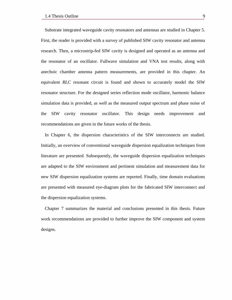
cutoff frequency of the dominant mode. Figure 2.1 presents the geometric parameters for
via diameter, via spacing, waveguide physical width, and substrate height as: d, s, w, and
h, respectively.
Fig. 2.1 The geometry of the SIW. Substrate thickness: h, waveguide physical width: w, via spacing: s, via diameter: d.
The transverse electric (TE) modes have no electric field components in the direction
of propagation, while the transverse magnetic (TM) modes have no magnetic field in the
direction of propagation. The transverse magnetic modes require longitudinal sidewall
surface currents to propagate. Similarly, TEmn transverse electric modes, where n ≠ 0,
require longitudinal sidewall surface currents for efficient propagation.
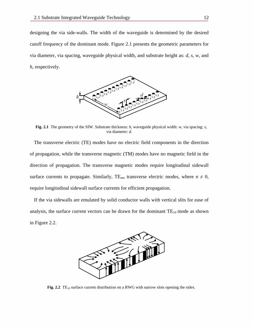
If the via sidewalls are emulated by solid conductor walls with vertical slits for ease of
analysis, the surface current vectors can be drawn for the dominant TE10 mode as shown
in Figure 2.2.
Fig. 2.2 TE10 surface current distribution on a RWG with narrow slots opening the sides.
2.1 Substrate Integrated Waveguide Technology 13
When the surface current is longitudinal along the sides of the waveguide, as is
the case for TM and TEmn, where n ≠ 0, modes, the vertical slots will cut through these
currents producing a large amount of radiation out of the sidewalls. Because of the
discontinuous structure of the sidewall, only TEm0 modes are supported in an SIW with
via sidewalls. It is shown in [2] that it is necessary to connect the metalized vias with a
conductive material to preserve the surface currents required for the propagation of TM
and TEmn, where n ≠ 0, modes.
The cutoff frequency for a conventional solid rectangular waveguide (RWG) with a
dielectric filling is given in Equation (2.1), where a, and b are the waveguide width, and
height, respectively [44].
𝑓𝑓𝑐𝑐 = 𝑐𝑐2𝜋𝜋√𝜀𝜀𝑟𝑟
��𝑚𝑚𝜋𝜋𝑎𝑎�
2+ �𝑛𝑛𝜋𝜋
𝑏𝑏�
2 (2.1)
In [45], it is shown that an SIW with via sidewalls is nearly identical to a rectangular
solid wall waveguide of similar width if a correction factor is taken into account for the
center-to-center via spacing. Equations for estimating the cutoff frequency for the first
two TEm0 modes of an SIW, based on the width correction factor, are given in [45]. The
width correction factor is defined as the effective width, weff, and is found by the least
square fitting of a set of fullwave simulation data. Equations (2.2) and (2.3) are
equivalent to Equation (2.1), where the width of the SIW is considered with the adjusted
value to account for the difference between the solid conductor sidewalls and the via
fence sidewalls.
2.1 Substrate Integrated Waveguide Technology 14
𝐹𝐹𝐶𝐶(TE 10 ) = 𝑐𝑐02√𝜀𝜀𝑟𝑟
∙ �𝑤𝑤 − 𝑑𝑑2
0.95𝑠𝑠�−1
(2.2)
𝐹𝐹𝐶𝐶(TE 20 ) = 𝑐𝑐0
√𝜀𝜀𝑟𝑟∙ �𝑤𝑤 − 𝑑𝑑
2
1.1𝑠𝑠− 𝑑𝑑
3
6.6𝑠𝑠�−1
(2.3)
These equations are valid for 𝑠𝑠 < 𝜆𝜆0√𝜀𝜀𝑟𝑟/2 and s < 4d [45].
In [38], a more accurate empirical equation is proposed to calculate the effective SIW
width. The effective width calculation allows designers to accurately determine the SIW
cutoff frequency once the via diameter and spacing are chosen. The effective width is
calculated by Equation (2.4), and is valid when s/d > 3 and d/w < 1/5. Once weff is
calculated, Equation (2.1) may be used to accurately determine the SIW cutoff frequency.
𝑤𝑤𝑒𝑒𝑓𝑓𝑓𝑓 = 𝑤𝑤 − 1.08 𝑑𝑑2
𝑠𝑠+ 0.1 𝑑𝑑2
𝑤𝑤 (2.4)
In [3], as mentioned earlier, it is proposed that the SIW may be considered as a
linear defect created in a 2-dimensional (2-D) EBG substrate that is composed of a
parallel-plate conductor pair periodically stitched together with metalized vias. Then, the
debate continues as to how many rows of the vias on the side of waveguide are sufficient
to contain the transmitted signal through the waveguide defect. The radiated power from
the via sidewall on the two sides of the waveguide is determined by calculating the total
transmitted and reflected power from the two ends of the waveguide. Thus, the scattering
parameter [S]-matrix is found by fullwave simulations. The total power neglecting
conductor and dielectric losses is calculated by Equation (2.5).
𝑃𝑃𝑡𝑡𝑡𝑡𝑡𝑡𝑎𝑎𝑡𝑡 = |𝑆𝑆11|2 + |𝑆𝑆21|2 (2.5)
2.1 Substrate Integrated Waveguide Technology 15
The authors of [3] refer to the waveguide as EBG-based waveguide and report less than
0.4% loss due to sidewall leakage for the case of either a single or double row of via
fence with only 0.1% more radiation in the case of a single via fence.
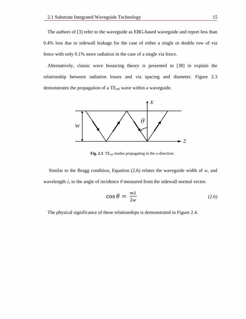
Alternatively, classic wave bouncing theory is presented in [38] to explain the
relationship between radiation losses and via spacing and diameter. Figure 2.3
demonstrates the propagation of a TEm0 wave within a waveguide.
Fig. 2.3 TEm0 modes propagating in the z-direction.
Similar to the Bragg condition, Equation (2.6) relates the waveguide width of w, and
wavelength λ, to the angle of incidence θ measured from the sidewall normal vector.
cos𝜃𝜃 = 𝑚𝑚𝜆𝜆2𝑤𝑤
(2.6)
The physical significance of these relationships is demonstrated in Figure 2.4.
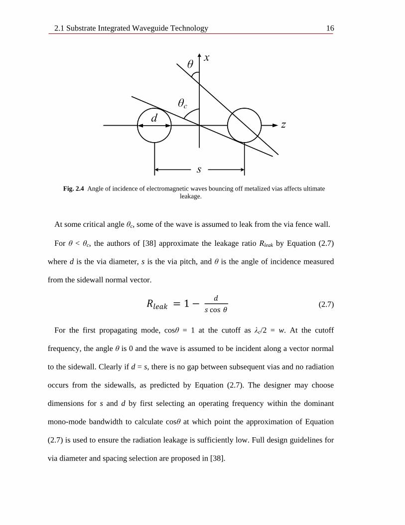
2.1 Substrate Integrated Waveguide Technology 16
Fig. 2.4 Angle of incidence of electromagnetic waves bouncing off metalized vias affects ultimate leakage.
At some critical angle θc, some of the wave is assumed to leak from the via fence wall.
For θ < θc, the authors of [38] approximate the leakage ratio Rleak by Equation (2.7)
where d is the via diameter, s is the via pitch, and θ is the angle of incidence measured
from the sidewall normal vector.
𝑅𝑅𝑡𝑡𝑒𝑒𝑎𝑎𝑙𝑙 = 1 − 𝑑𝑑𝑠𝑠 cos 𝜃𝜃
(2.7)
For the first propagating mode, cosθ = 1 at the cutoff as λc/2 = w. At the cutoff
frequency, the angle θ is 0 and the wave is assumed to be incident along a vector normal
to the sidewall. Clearly if d = s, there is no gap between subsequent vias and no radiation
occurs from the sidewalls, as predicted by Equation (2.7). The designer may choose
dimensions for s and d by first selecting an operating frequency within the dominant
mono-mode bandwidth to calculate cosθ at which point the approximation of Equation
(2.7) is used to ensure the radiation leakage is sufficiently low. Full design guidelines for
via diameter and spacing selection are proposed in [38].
2.1 Substrate Integrated Waveguide Technology 17 2.1.3 Surface Currents and Supported Modes
To characterize the modes supported in substrate integrated waveguides, first a
rectangular waveguide is simulated using Ansoft High Frequency Structure Simulator
(HFSS). The dimensions of the waveguide are a = 1.3mm, b = 0.635mm, and length l =
10mm. The dielectric material filling the waveguide is Rogers RO3006. To analyze the
excitation of higher-order modes and surface current distributions, conductor and
dielectric losses in the substrate are eliminated to decrease simulation time. The Rogers
3006 substrate is considered to be perfect dielectric, with the dielectric permittivity of
6.15. Wave ports, as explained in the Ansoft HFSS user manual [46], are assigned to both
ends of the waveguide and 5 modes are excited.
In MATLAB, the cutoff frequencies for the first 5 modes are calculated using Equation
(2.1) and listed in Table (2.1).
TABLE 2.1 CUTOFF FREQUENCIES OF HIGHER ORDER MODES FOUND ANALYTICALLY
TE10 TE20 TE01 TE11 TM11
fc = 46GHz fc = 93GHz fc = 95GHz fc = 106GHz fc = 106GHz
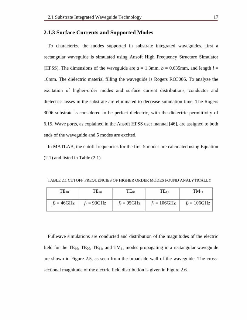
Fullwave simulations are conducted and distribution of the magnitudes of the electric
field for the TE10, TE20, TE11, and TM11 modes propagating in a rectangular waveguide
are shown in Figure 2.5, as seen from the broadside wall of the waveguide. The cross-
sectional magnitude of the electric field distribution is given in Figure 2.6.
2.1 Substrate Integrated Waveguide Technology 18
(a) (b)
(c) (d)
Fig. 2.5 Magnitude of electric field for (a) TE10, (b) TE20, (c) TE11 , and (d) TM11 , on the broadside wall
of the rectangular waveguide, at 110GHz.
(a) (b)
(c) (d)
Fig. 2.6 Magnitude of electric field for (a) TE10, (b) TE20, (c) TE11, and (d) TM11, at the cross-section of
the rectangular waveguide, at 110GHz. The electric field distributions match those given in literature [44].

2.1 Substrate Integrated Waveguide Technology 19
As discussed in Section 2.1.2, the SIW interconnects with via fence sidewalls only
support the TEm0 modes. The propagating modes are further studied by investigating the
surface currents supported by the structure using analytical equations and fullwave
simulations. From the relations of current and magnetic field in Ampere’s circuital law it
is possible to determine the direction of surface current. If a surface current cannot flow
in a particular direction, it can be deduced that a magnetic field perpendicular to that
surface current is not supported. Thus, a mode requiring such a surface current will not
propagate.
𝐽𝐽𝑠𝑠��⃑ = 𝑛𝑛� × �𝐻𝐻��𝑥𝑥 𝑡𝑡𝑟𝑟 𝑦𝑦=0 (2.8)
Equation (2.8) demonstrates the relation between surface current and the cross product
of a vector normal to that surface and the magnetic field [44].
The relations describing the magnetic field for TE10 are found from solutions to
Maxwell’s equations, considering the waveguide structure to set boundary conditions.
𝐻𝐻𝑦𝑦 = 0 (2.9)
𝐻𝐻𝑥𝑥 = 𝑗𝑗𝑗𝑗𝜋𝜋𝑙𝑙𝑐𝑐2𝑎𝑎
𝐴𝐴10 sin 𝜋𝜋𝑥𝑥𝑎𝑎𝑒𝑒−𝑗𝑗𝑗𝑗𝑗𝑗 (2.10)
𝐻𝐻𝑗𝑗 = 𝐴𝐴10 cos 𝜋𝜋𝑥𝑥𝑎𝑎𝑒𝑒−𝑗𝑗𝑗𝑗𝑗𝑗 (2.11)
𝐽𝐽𝑠𝑠𝑇𝑇𝑇𝑇10����������⃑ = �⃑�𝑥 × 𝑗𝑗𝐻𝐻𝑗𝑗 = −�⃑�𝑦𝐻𝐻𝑗𝑗 (2.12)
Equation (2.12) clearly demonstrates the direction of surface current along the sidewall
is solely vertical (y-direction) for the TE10 mode.
2.1 Substrate Integrated Waveguide Technology 20
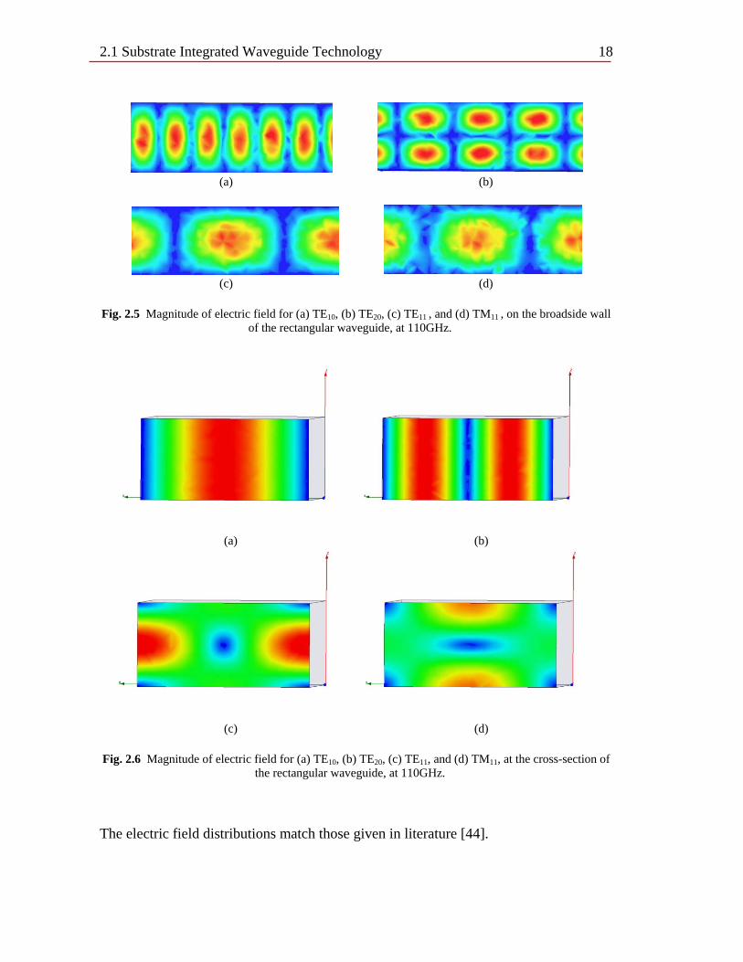
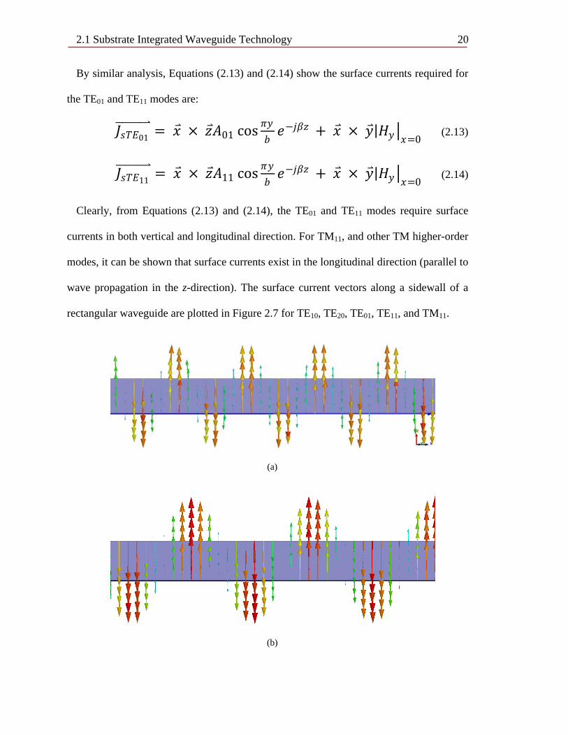
By similar analysis, Equations (2.13) and (2.14) show the surface currents required for
the TE01 and TE11 modes are:
𝐽𝐽𝑠𝑠𝑇𝑇𝑇𝑇01����������⃑ = �⃑�𝑥 × 𝑗𝑗𝐴𝐴01 cos 𝜋𝜋𝑦𝑦
𝑏𝑏𝑒𝑒−𝑗𝑗𝑗𝑗𝑗𝑗 + ��⃑�𝑥 × �⃑�𝑦|�𝐻𝐻𝑦𝑦 �𝑥𝑥=0
(2.13)
𝐽𝐽𝑠𝑠𝑇𝑇𝑇𝑇11����������⃑ = �⃑�𝑥 × 𝑗𝑗𝐴𝐴11 cos 𝜋𝜋𝑦𝑦
𝑏𝑏𝑒𝑒−𝑗𝑗𝑗𝑗𝑗𝑗 + ��⃑�𝑥 × �⃑�𝑦|�𝐻𝐻𝑦𝑦 �𝑥𝑥=0
(2.14)
Clearly, from Equations (2.13) and (2.14), the TE01 and TE11 modes require surface
currents in both vertical and longitudinal direction. For TM11, and other TM higher-order
modes, it can be shown that surface currents exist in the longitudinal direction (parallel to
wave propagation in the z-direction). The surface current vectors along a sidewall of a
rectangular waveguide are plotted in Figure 2.7 for TE10, TE20, TE01, TE11, and TM11.
(a)
(b)
2.1 Substrate Integrated Waveguide Technology 21
(c)
(d)
(e)
Fig. 2.7 Surface current vectors along a sidewall of a rectangular waveguide for (a) TE10, (b) TE20, (c) TE01, (d) TE11, and (e) TM11, at 110GHz
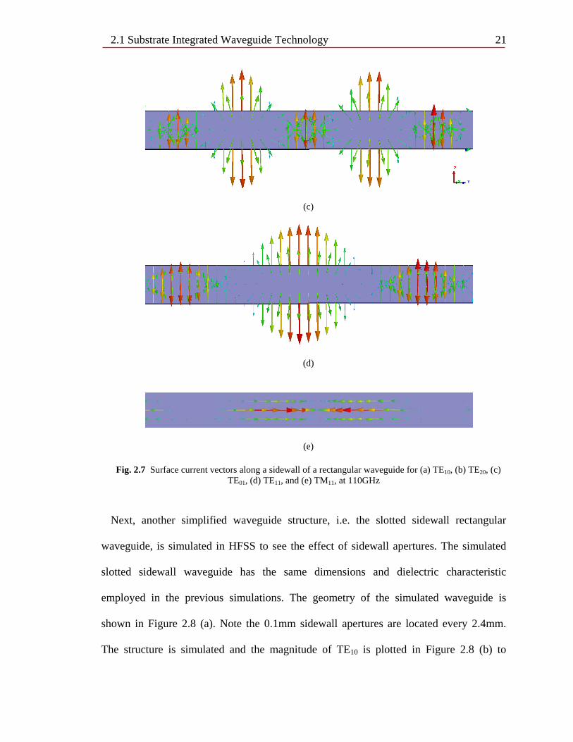
Next, another simplified waveguide structure, i.e. the slotted sidewall rectangular
waveguide, is simulated in HFSS to see the effect of sidewall apertures. The simulated
slotted sidewall waveguide has the same dimensions and dielectric characteristic
employed in the previous simulations. The geometry of the simulated waveguide is
shown in Figure 2.8 (a). Note the 0.1mm sidewall apertures are located every 2.4mm.
The structure is simulated and the magnitude of TE10 is plotted in Figure 2.8 (b) to
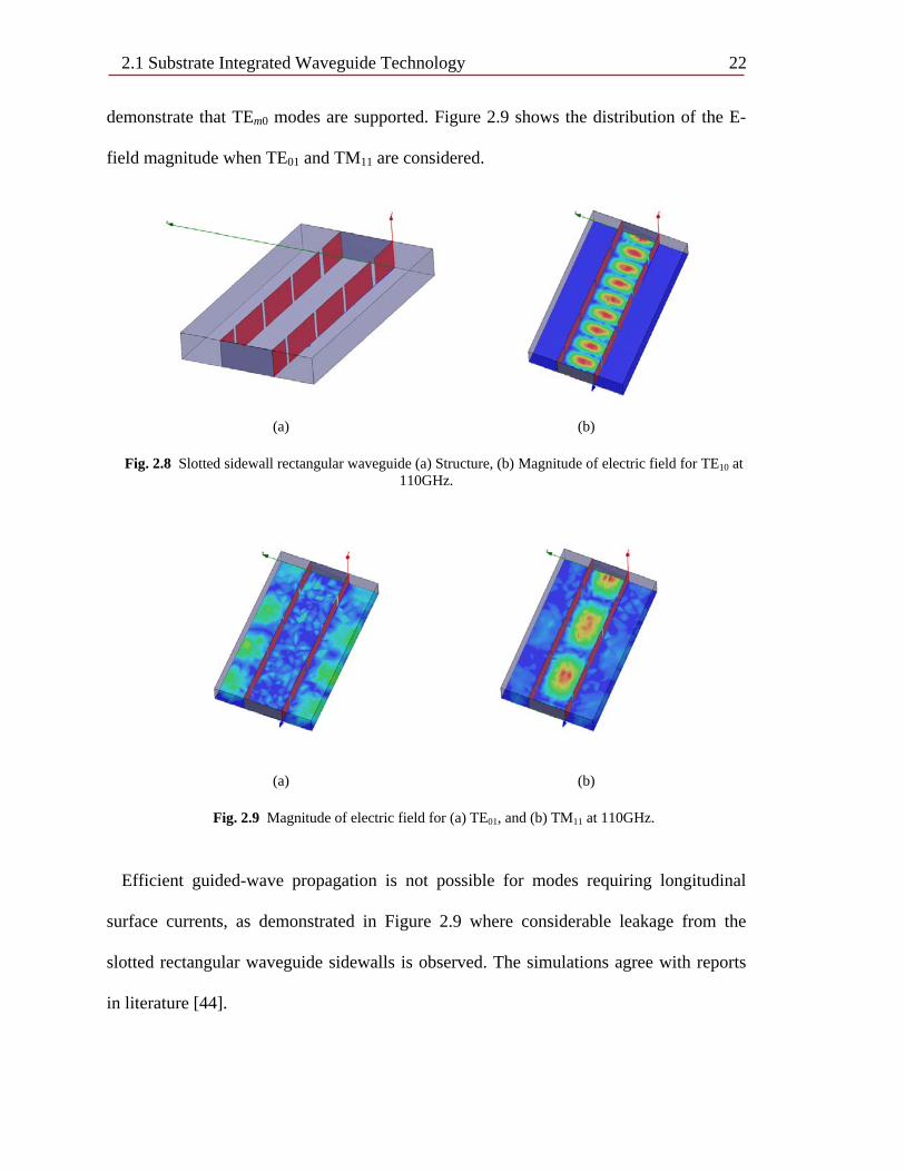
2.1 Substrate Integrated Waveguide Technology 22 demonstrate that TEm0 modes are supported. Figure 2.9 shows the distribution of the E-
field magnitude when TE01 and TM11 are considered.
(a) (b)
Fig. 2.8 Slotted sidewall rectangular waveguide (a) Structure, (b) Magnitude of electric field for TE10 at 110GHz.
(a) (b)
Fig. 2.9 Magnitude of electric field for (a) TE01, and (b) TM11 at 110GHz.
Efficient guided-wave propagation is not possible for modes requiring longitudinal
surface currents, as demonstrated in Figure 2.9 where considerable leakage from the
slotted rectangular waveguide sidewalls is observed. The simulations agree with reports
in literature [44].
2.1 Substrate Integrated Waveguide Technology 23
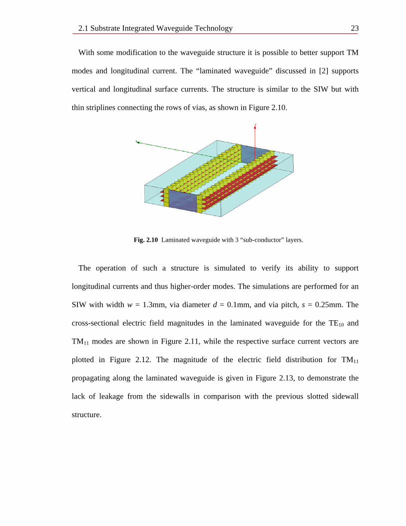
With some modification to the waveguide structure it is possible to better support TM
modes and longitudinal current. The “laminated waveguide” discussed in [2] supports
vertical and longitudinal surface currents. The structure is similar to the SIW but with
thin striplines connecting the rows of vias, as shown in Figure 2.10.
Fig. 2.10 Laminated waveguide with 3 “sub-conductor” layers.
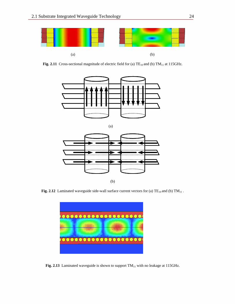
The operation of such a structure is simulated to verify its ability to support
longitudinal currents and thus higher-order modes. The simulations are performed for an
SIW with width w = 1.3mm, via diameter d = 0.1mm, and via pitch, s = 0.25mm. The
cross-sectional electric field magnitudes in the laminated waveguide for the TE10 and
TM11 modes are shown in Figure 2.11, while the respective surface current vectors are
plotted in Figure 2.12. The magnitude of the electric field distribution for TM11
propagating along the laminated waveguide is given in Figure 2.13, to demonstrate the
lack of leakage from the sidewalls in comparison with the previous slotted sidewall
structure.
2.1 Substrate Integrated Waveguide Technology 24
(a) (b)
Fig. 2.11 Cross-sectional magnitude of electric field for (a) TE10 and (b) TM11 at 115GHz.
(a)
(b)
Fig. 2.12 Laminated waveguide side-wall surface current vectors for (a) TE10 and (b) TM11 .
Fig. 2.13 Laminated waveguide is shown to support TM11 with no leakage at 115GHz.
2.2 Substrate Integrated Waveguide Transitions 25
2.2 Substrate Integrated Waveguide Transitions
The interconnection of rectangular waveguides to printed circuit components is a
system integration obstacle. The microstrip transmission line is commonly used in PCBs
for signal routing as it possesses an exposed trace that is very easy to interface with
integrated circuits, connectors, and packaged components. The microstrip is simply
terminated in a through hole via or a printed conductor pad to connect to the package.
Likewise, to interface with an off-board device through an edge launch coaxial SMA
connector, the microstrip is easily run from planar circuitry to the necessary board edge
pad. As the microstrip transmission line only has one ground conductor, the cross
sectional electric field distribution propagates through both the substrate and the media
above the substrate (usually air). Thus, the microstrip is said to propagate a quasi-TEM
mode, in comparison to a pure transverse electromagnetic (TEM) line, such as a stripline
[44]. In order to interconnect rectangular waveguides to planar transmission lines, an
electromagnetic mode conversion must be accomplished to transmit signals between the
planar TEM, or quasi-TEM, transmission line and the guided waveguide mode. The
characteristic impedance of the planar transmission lines must be simultaneously matched
to the frequency dependent wave impedance that relates the transverse electric and
magnetic fields of the waveguide, as given in Equation (2.15) [44].
𝑍𝑍𝑇𝑇𝑇𝑇 = 𝑇𝑇𝑥𝑥𝐻𝐻𝑦𝑦
= −𝑇𝑇𝑦𝑦𝐻𝐻𝑥𝑥
= 𝑙𝑙𝑘𝑘𝑗𝑗
(2.15)
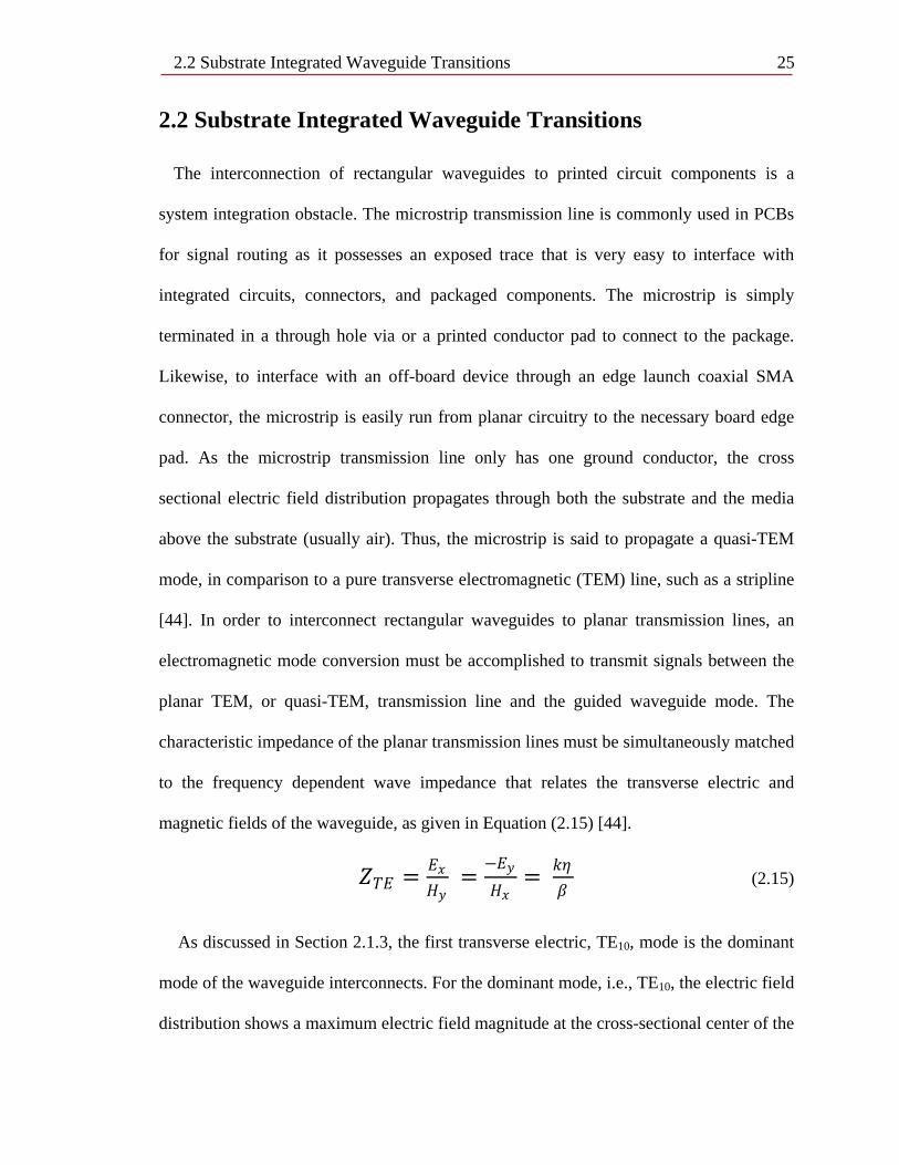
As discussed in Section 2.1.3, the first transverse electric, TE10, mode is the dominant
mode of the waveguide interconnects. For the dominant mode, i.e., TE10, the electric field
distribution shows a maximum electric field magnitude at the cross-sectional center of the
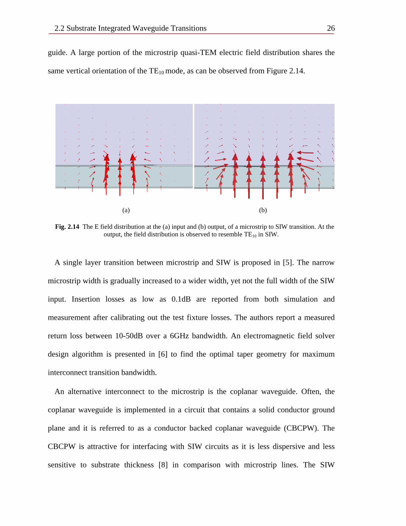
2.2 Substrate Integrated Waveguide Transitions 26 guide. A large portion of the microstrip quasi-TEM electric field distribution shares the
same vertical orientation of the TE10 mode, as can be observed from Figure 2.14.
(a) (b)
Fig. 2.14 The E field distribution at the (a) input and (b) output, of a microstrip to SIW transition. At the
output, the field distribution is observed to resemble TE10 in SIW.
A single layer transition between microstrip and SIW is proposed in [5]. The narrow
microstrip width is gradually increased to a wider width, yet not the full width of the SIW
input. Insertion losses as low as 0.1dB are reported from both simulation and
measurement after calibrating out the test fixture losses. The authors report a measured
return loss between 10-50dB over a 6GHz bandwidth. An electromagnetic field solver
design algorithm is presented in [6] to find the optimal taper geometry for maximum
interconnect transition bandwidth.
An alternative interconnect to the microstrip is the coplanar waveguide. Often, the
coplanar waveguide is implemented in a circuit that contains a solid conductor ground
plane and it is referred to as a conductor backed coplanar waveguide (CBCPW). The
CBCPW is attractive for interfacing with SIW circuits as it is less dispersive and less
sensitive to substrate thickness [8] in comparison with microstrip lines. The SIW
2.2 Substrate Integrated Waveguide Transitions 27 interconnects exhibit lower conductor loss due to the larger copper area carrying the
signal currents when a thicker substrate is used. Field leakage increases in microstrip
transmission lines as substrate thickness is increased [8]. For very thick substrates,
microstrip lines are prone to radiating to higher order substrate modes when carrying high
frequency signals. A multilayer CPW to SIW transition is proposed in [9]. A vertical
current probe is implemented, achieving a 0.9dB insertion loss from 19GHz to 40GHz
with a return loss better than 10dB over a 70% fractional bandwidth.
A far simpler CBCPW to SIW transition is presented in [8] that shares a similar
geometry to that of the microstrip transition. Similar to the microstrip transmission line,
the CBCPW has some vertical electric field distribution that is used to excite the SIW
interconnect. The presented CBCPW taper exhibits an insertion loss lower than 0.4dB
with a return loss better than 20dB over the entire Ka band. The simple taper geometry
negates the need for multilayer PCB fabrication and does not require any vertical current
probes which are highly prone to EMI. One issue the designer must consider is the
coupling to parallel-plate, slot-line, or resonant patch modes in the CBCPW section [8].
These pitfalls are easily avoided in the presence of SIW technology where the via array
sidewalls may be extended to follow the path of the CBCPW transmission line to short
the signal plane ground sections to the bottom solid ground plane. A similar geometry is
simultaneously presented at the 2009 IEEE International Microwave Symposium (IMS)
in [10].
2.3 Reducing the Footprint of Substrate Integrated Waveguides 28
2.3 Reducing the Footprint of Substrate Integrated Waveguides
Waveguide interconnects are necessary components in space exploration
communication systems and satellites. A milled metallic waveguide is a large weight
payload to incorporate into a space craft. Therefore, waveguide miniaturization is an
attractive research area. Waveguide miniaturization has existed for decades. By adding
fins, ridges, and T-shaped septums to milled rectangular waveguides, microwave
engineers are able to design interconnects with decreased overall dimensions and width.
The dominant mode electric field is forced to propagate in a new modified configuration,
depending on the metallic obstacle introduced to the broad or narrow wall. In [47], the
authors introduce a double T-septum waveguide whose two broad wall metallic T-shaped
inserts force the dominant mode electric field to fold around the inserts allowing for an
overall narrower interconnect footprint. Not only does the proposed double T-septum
waveguide decrease the interconnect dimension and weight; it has little effect on the
cutoff frequency of the second TE20 mode. The result is an extension of the dominant
mode operating bandwidth. The milling required in manufacturing the fins and T-septum
inserts must be very precise to ensure the designed performance is achieved. While the
above advancements in payload reduction provide the ability to create lighter satellites
and space craft for longer mission life with the same fuel quantities, even further weight
and size decreases are realized by entering the substrate integrated environment. By
introducing a dielectric filling within the waveguide, a width reduction on the order of
√𝜀𝜀𝑟𝑟−1 is achieved. In comparison to other PCB transmission lines such as the
microstrips, CPWs, and striplines, the SIW interconnects possess a significantly larger
2.3 Reducing the Footprint of Substrate Integrated Waveguides 29 footprint. In recent years, researchers have proposed several methods to reduce the
relatively large SIW width.
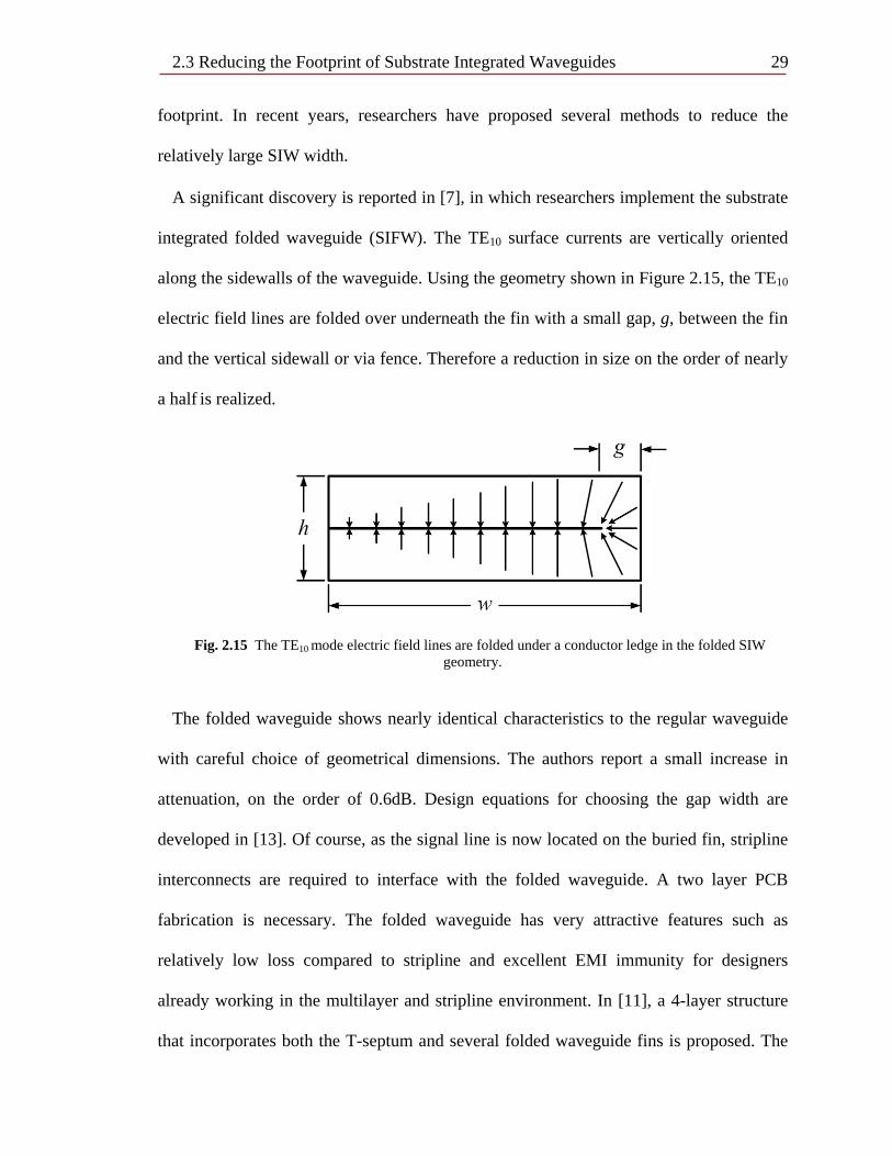
A significant discovery is reported in [7], in which researchers implement the substrate
integrated folded waveguide (SIFW). The TE10 surface currents are vertically oriented
along the sidewalls of the waveguide. Using the geometry shown in Figure 2.15, the TE10
electric field lines are folded over underneath the fin with a small gap, g, between the fin
and the vertical sidewall or via fence. Therefore a reduction in size on the order of nearly
a half is realized.
Fig. 2.15 The TE10 mode electric field lines are folded under a conductor ledge in the folded SIW geometry.
The folded waveguide shows nearly identical characteristics to the regular waveguide
with careful choice of geometrical dimensions. The authors report a small increase in
attenuation, on the order of 0.6dB. Design equations for choosing the gap width are
developed in [13]. Of course, as the signal line is now located on the buried fin, stripline
interconnects are required to interface with the folded waveguide. A two layer PCB
fabrication is necessary. The folded waveguide has very attractive features such as
relatively low loss compared to stripline and excellent EMI immunity for designers
already working in the multilayer and stripline environment. In [11], a 4-layer structure
that incorporates both the T-septum and several folded waveguide fins is proposed. The
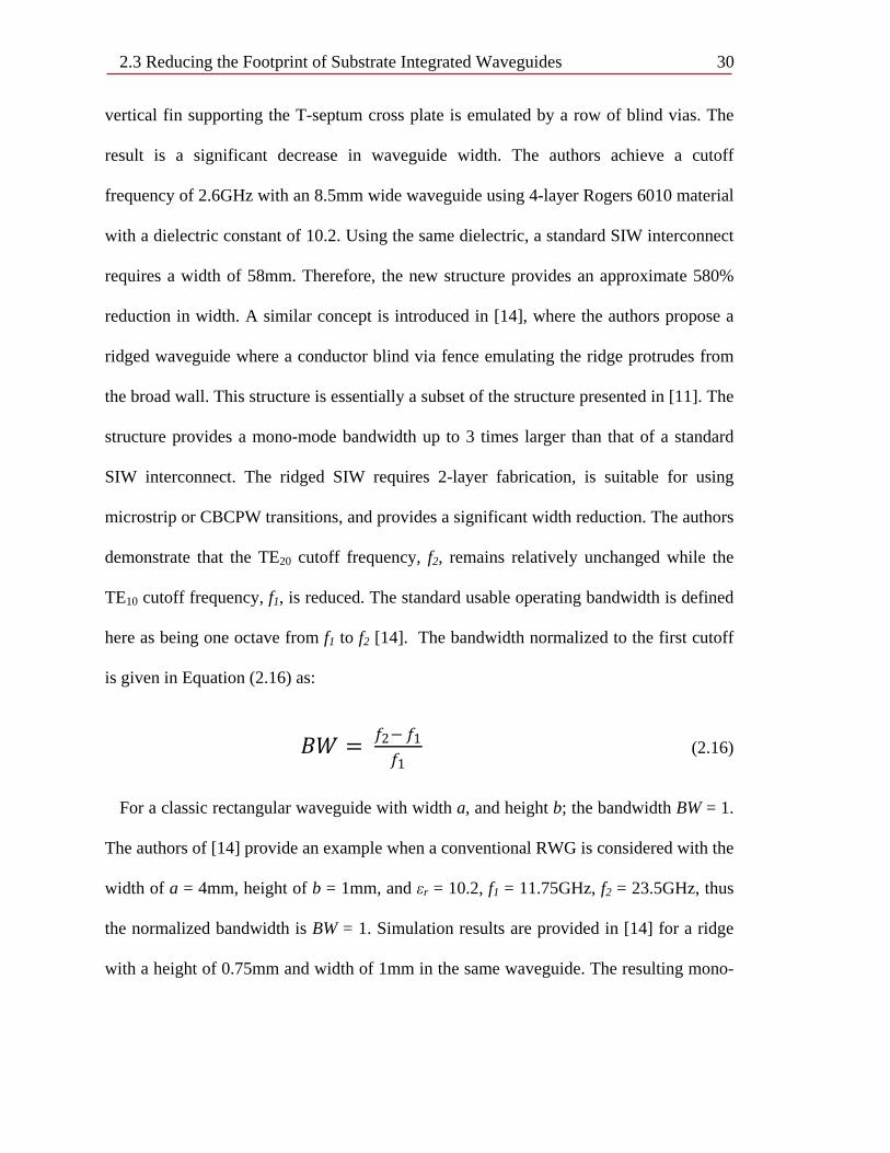
2.3 Reducing the Footprint of Substrate Integrated Waveguides 30 vertical fin supporting the T-septum cross plate is emulated by a row of blind vias. The
result is a significant decrease in waveguide width. The authors achieve a cutoff
frequency of 2.6GHz with an 8.5mm wide waveguide using 4-layer Rogers 6010 material
with a dielectric constant of 10.2. Using the same dielectric, a standard SIW interconnect
requires a width of 58mm. Therefore, the new structure provides an approximate 580%
reduction in width. A similar concept is introduced in [14], where the authors propose a
ridged waveguide where a conductor blind via fence emulating the ridge protrudes from
the broad wall. This structure is essentially a subset of the structure presented in [11]. The
structure provides a mono-mode bandwidth up to 3 times larger than that of a standard
SIW interconnect. The ridged SIW requires 2-layer fabrication, is suitable for using
microstrip or CBCPW transitions, and provides a significant width reduction. The authors
demonstrate that the TE20 cutoff frequency, f2, remains relatively unchanged while the
TE10 cutoff frequency, f1, is reduced. The standard usable operating bandwidth is defined
here as being one octave from f1 to f2 [14]. The bandwidth normalized to the first cutoff
is given in Equation (2.16) as:
𝐵𝐵𝐵𝐵 = 𝑓𝑓2− 𝑓𝑓1𝑓𝑓1
(2.16)
For a classic rectangular waveguide with width a, and height b; the bandwidth BW = 1.
The authors of [14] provide an example when a conventional RWG is considered with the
width of a = 4mm, height of b = 1mm, and εr = 10.2, f1 = 11.75GHz, f2 = 23.5GHz, thus
the normalized bandwidth is BW = 1. Simulation results are provided in [14] for a ridge
with a height of 0.75mm and width of 1mm in the same waveguide. The resulting mono-
2.3 Reducing the Footprint of Substrate Integrated Waveguides 31 mode bandwidth properties are observed as follows: f1 = 6.7GHz, f2 = 26.5GHz, BW =
2.96. A bandwidth increase of 196% is observed.
Another attempt at miniaturization is documented in [12] with the introduction of a
half-mode SIW (HMSIW). The half-mode SIW is able to propagate guided waves in only
half the width of the standard SIW. The symmetric plane along the direction of
transmission is considered a perfect magnetic wall. Guided propagation is unchanged
when cutting through the magnetic wall. The HMSIW interconnects require slightly more
than half of the SIW width to operate with the same cutoff frequency, as can be observed
in Figure 2.16 where the SIW is truncated at the lower edge of the microstrip. In this
configuration, the added width required is equal to half of the microstrip width. The
HMSIW is particularly beneficial in that it only requires a single layer PCB fabrication,
at the expense of some EMI susceptibility on one open side.
Fig. 2.16 HMSIW interconnect.
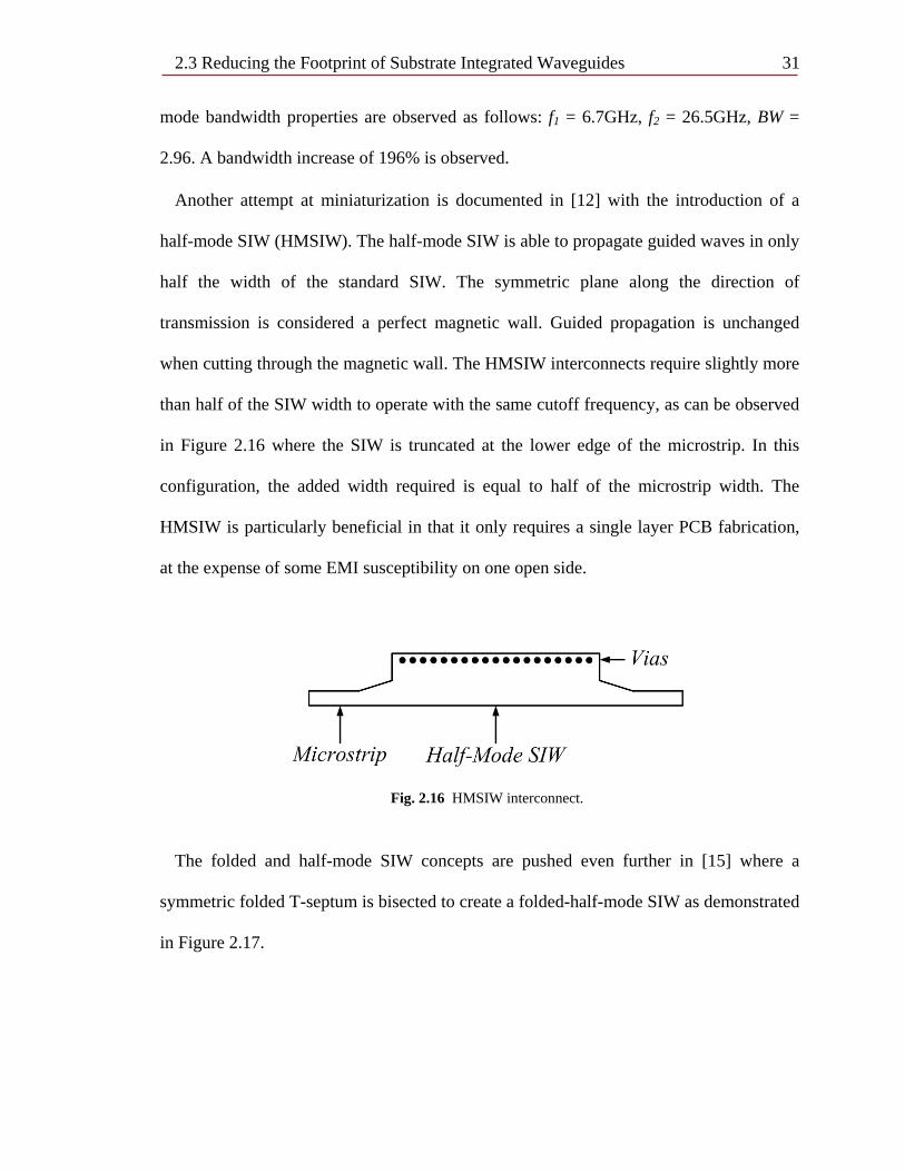
The folded and half-mode SIW concepts are pushed even further in [15] where a
symmetric folded T-septum is bisected to create a folded-half-mode SIW as demonstrated
in Figure 2.17.
2.3 Reducing the Footprint of Substrate Integrated Waveguides 32
Fig. 2.17 FHMSIW (T-Septum) interconnect.
2.4 Summary
In this chapter a comprehensive overview of SIW interconnects is presented. It has
been shown how the SIW interconnects are able to propagate the TEn0 modes by an in
depth analysis of the surface currents supported by SIW structure. By including
longitudinal metallic strips connecting the via sidewalls, the SIW interconnects will
support higher order TM modes. SIW transitions are studied, as well as miniaturization
techniques to decrease the overall footprint of the SIW layout.
33
Chapter 3 Substrate Integrated Waveguide-Based Components 3.1 Introduction
Since the introduction of SIW technology various SIW-based circuit components have
been developed. SIW-based power dividers, routing elements like bends, filters, couplers,
as well as resonant cavities and antennas have all been explored [3], [15-33], [48].
Research has shown that it is possible to use the substrate integrated waveguide
principles to create novel communication system components such as oscillators, up-
converters, and even radar front-end receivers [35], [43], [49]. With the emerging
developments of the SIW-based components and circuits, the design of an entire
communication system based on these new interconnects seems possible. In this chapter,
a few critical circuit components such as SIW filters, cavity resonators, and couplers have
been studied.
3.2 SIW Filters and Cavity Resonators 34
3.2 SIW Filters and Cavity Resonators
Microwave filters are generally two port devices designed to provide some
transmission and attenuation properties at different frequencies depending on the
requirements of the system. There are several filter topologies that can be broken down
into the following categories: low-pass, high-pass, bandpass, bandstop, notch, and all-
pass. The waveguide-based interconnects are naturally high-pass devices due to the high
attenuation of the dominant propagating mode below its cutoff frequency. However, by
applying some geometrical modifications, bandpass or bandstop filtering functions can be
achieved. Often in microwave networks, a channel or band-select device is needed to
eliminate unwanted signals from the system, thus, one of the most commonly researched
SIW-based filter topologies is the bandpass type.
A popular microwave filter design methodology involves the cascading of periodic unit
cells that possess the required capacitive and inductive equivalent elements to achieve the
filter design criteria. In waveguides, following a similar approach, a filter can be
implemented by using properly designed coupled waveguide cavities in order to
synthesize the required filter function. Cavity resonators are basically selective bandpass
filters that can be approximated with RLC circuits. Many of the proposed SIW filters are
composed of coupled SIW cavity resonators. Therefore, the filter discussion herein is
preceded by an explanation of SIW cavity resonators and the great contribution of these
new building blocks to the world of microwave and mm-wave circuit design.
3.2 SIW Filters and Cavity Resonators 35 3.2.1 SIW Cavity Resonators
The development of SIW-based cavity resonators marks a significant new era in
microwave engineering. Microwave voltage controlled oscillators (VCO) often require a
resonator with a high-quality factor to produce low-noise high-frequency tones.
Conventionally, dielectric resonators are made from a high-dielectric substrate and must
be adhesively mounted to a PCB. The dielectric puck is then coupled to one or more
microstrip lines to create either a series or parallel feedback resonator that is included in a
planar circuit such as a single transistor VCO. The design of SIW cavity resonators is
first presented in [24], and later in [25]. By adding a row of vias to terminate the SIW, the
number of half wave field variations in the z-direction is now limited. By exploiting the
TE101 mode, a dominant resonance is produced.
𝑓𝑓𝑚𝑚𝑛𝑛𝑡𝑡 = 𝑐𝑐2𝜋𝜋√𝜇𝜇𝑟𝑟𝜀𝜀𝑟𝑟
�� 𝑚𝑚𝜋𝜋𝑤𝑤𝑒𝑒𝑓𝑓𝑓𝑓
�2
+ �𝑛𝑛𝜋𝜋𝑏𝑏�
2+ � 𝑡𝑡𝜋𝜋
𝑡𝑡𝑒𝑒𝑓𝑓𝑓𝑓�
2 (3.1)
𝑡𝑡𝑒𝑒𝑓𝑓𝑓𝑓 = 𝑡𝑡𝑒𝑒𝑛𝑛𝑙𝑙𝑡𝑡ℎ + 𝑑𝑑2
0.95𝑠𝑠 (3.2)
Equation (3.1) represents the cutoff frequency for a given mode in a 3-dimensional
cavity. It is the resonance frequency equation for a rectangular waveguide cavity with
adjustments made for the width, see Equation (2.4), and length, see Equation (3.2), of the
cavity generated by the rows of vias, as given in [35, 38]. The first strategy to couple a
signal to the cavity is by using a current probe, in which a microstrip or CPW is
terminated into a gap in the side of the SIW cavity walls [25]. A current probe fed SIW
rectangular cavity is simulated in HFSS to observe the cavity resonance. An arbitrarily
sized cavity is chosen with dimensions of 10.75mm x 11mm x 0.635mm and dielectric
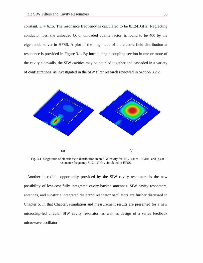
3.2 SIW Filters and Cavity Resonators 36 constant, εr = 6.15. The resonance frequency is calculated to be 8.1241GHz. Neglecting
conductor loss, the unloaded Q, or unloaded quality factor, is found to be 400 by the
eigenmode solver in HFSS. A plot of the magnitude of the electric field distribution at
resonance is provided in Figure 3.1. By introducing a coupling section in one or more of
the cavity sidewalls, the SIW cavities may be coupled together and cascaded in a variety
of configurations, as investigated in the SIW filter research reviewed in Section 3.2.2.
(a) (b)
Fig. 3.1 Magnitude of electric field distribution in an SIW cavity for TE101 (a) at 10GHz, and (b) at resonance frequency 8.1241GHz , simulated in HFSS.
Another incredible opportunity provided by the SIW cavity resonators is the new
possibility of low-cost fully integrated cavity-backed antennas. SIW cavity resonators,
antennas, and substrate integrated dielectric resonator oscillators are further discussed in
Chapter 5. In that Chapter, simulation and measurement results are presented for a new
microstrip-fed circular SIW cavity resonator, as well as design of a series feedback
microwave oscillator.
3.2 SIW Filters and Cavity Resonators 37 3.2.2 SIW Bandpass Filters
The bandpass filters are the most commonly studied SIW-based filters. As the SIW is
naturally a high-pass interconnect, the filter designer must introduce elements to provide
the upper break frequency. As the minimum waveguide width is dependent on the cutoff
frequency of the dominant mode, using the cutoff frequency as the lower filter break
frequency results in the most compact filter. In [27], the authors propose a 2-D SIW
cavity filter that is able to generate finite transmission zeros to achieve the desired
stopband characteristic. It is referred to as a folded filter as the input and output are side-
by-side with opposite directions of propagation. The measured results show good
selectivity in the X-band from 9.62GHz to 9.71GHz with an insertion loss of -2.1dB at
9.68GHz and a return loss below 19.5dB.
In [28], a series of multiple passband bandpass filters are presented based on the
Chebyshev low-pass prototype and quasi-elliptic responses. A possible application of the
proposed filters is in a system utilizing upper and lower sideband modulated data to filter
both the carrier and any up-converted low frequency noise.
A bandpass filter based on the 2-layer folded waveguides is presented in [29]. A folded
waveguide cavity is introduced and four cavities are implemented to realize a pseudo-
elliptical transfer function with four poles and two transmission zeros. A negative
coupling structure is achieved by cutting a slot between the adjacent input and output
cavities in the middle conductor that makes up the folded cavity fins. The proposed filter
has an insertion loss of 1.6dB, return loss of 20dB, and adjacent channel selectivity of
25dB.
3.2 SIW Filters and Cavity Resonators 38
A patent pending SIW bandpass filter optimized for high stopband rejection is
presented in [30] for use in critical ground to satellite communication systems where out
of band content must be sufficiently suppressed. Filter performance is guaranteed from -
20°C to +40°C with an insertion loss of 0.9dB in the 19.2GHz to 21.2GHz passband. The
passband return loss is better than 18dB where out of band rejection between 29.5GHz
and 30GHz is over 50dB. The filters are subject to rigorous simulation of the stopband
performance. The authors demonstrate via simulation results how the electric field
magnitude distribution at 29.23GHz for an input excitation of 1W is completely filtered
by the patent pending SIW filter topology.
Another SIW-based bandpass filter is presented in [50] for the European UWB network
emissions mask, while a compact HMSIW bandpass filter is presented in [51]. All of the
proposed SIW bandpass filters show promising applications in high performance
microwave and millimeter-wave communication systems.
3.2.3 Evanescent Mode Filters
Evanescent mode filters are an intriguing branch of waveguide filters that make use of
waveguide sections operating below cutoff, separated by capacitive obstacles inserted in
the guide. A common evanescent mode filter implemented in microwave systems is
comprised of a waveguide with inline protruding screws of various heights. The
equivalent circuit of an evanescent mode filter represents the cutoff sections as series
inductances and the broad wall protruding posts, ridges, or T-septums as shunt
capacitances. Depending on the capacitive obstacle’s physical geometry, the electric field
folds around that obstacle much like the ridge and T-septum waveguides. At the point of
3.2 SIW Filters and Cavity Resonators 39 the protruding obstacle, the waveguide is operated above the cutoff frequency of the
dominant mode. In between the protruding obstacles, the waveguide is operated below
the cutoff frequency of the dominant mode. As these filters operate like a waveguide
below its cutoff frequency, they propagate evanescent modes. Clearly, in a classic
rectangular waveguide, implementing the obstacles with tunable posts yields adjustable
filters that significantly reduce the stress of tight manufacturing tolerances. Of course, in
the substrate integrated environment it is not very practical to mount tuning screws in an
SIW as the waveguide height is often less than 1mm. With modern PCB fabrication
technology, precise SIW ridges and T-Septums are efficiently produced at a significantly
lower cost.
In [52], the first SIW ridge and T-septum based evanescent mode filters are presented.
The proposed 3rd order evanescent mode bandpass filters have a width of 14mm yet have
a cutoff of only 1.67GHz for the T-Septum sections and 4.79GHz for the ridged SIW
sections. The proposed filter shows a 1.3dB insertion loss at a center frequency of
2.45GHz with a 200MHz passband with 14.3dB return loss.
Evanescent mode filters are known for their high stopband rejection. In comparison to
the patent pending SIW filter for ground to satellite applications, the proposed evanescent
mode filter shows far greater stopband attenuation.
3.2.4 All-pass Filters
For all of the filters previously discussed, the goal is to modify the magnitude response
of a two-port microwave network to fit some pre-determined requirement. The
microwave engineer must pay close attention to the group delay of a designed filter so as
to avoid distortion due to dispersion for broadband transmissions. There also exists the

3.2 SIW Filters and Cavity Resonators 40 case where the phase of a signal must be modified while the amplitude remains constant.
An all-pass filter is a microwave network designed to pass signals from input to output
with some predetermined phase transfer function, while the amplitude response remains
flat. Substrate integrated waveguides are dispersive interconnects. The group delay is not
constant for all frequencies in any waveguide. In fact, a large group delay is observed at
the cutoff and near cutoff frequencies which gradually approaches the ideally constant
case for a TEM line. All-pass filters designed to correct the dispersive phase transfer
function of the SIW interconnects are presented in Chapter 6.
3.3 SIW Directional Couplers and Hybrid Junctions
Directional couplers are common passive devices used to route, divide, and combine
signals in microwave systems. Three-port power dividers are discussed in more detail in
Chapter 4. Waveguide directional couplers are four-port devices with ports for input feed,
through line, coupled line, and an isolated port. The through and coupled ports are
generally designed to be 90° (quadrature) or 180° (magic-T or rat race) out of phase from
each other when excited from the input port [44]. The [S] matrix for the symmetrical
coupler is given in (3.3). While the [S] matrix for the asymmetrical coupler is given in
Equation (3.4). Note: α and β are real and 𝛼𝛼2 + 𝑗𝑗2 = 1.
[𝑆𝑆] = �
0 𝛼𝛼𝛼𝛼 0
𝑗𝑗𝑗𝑗 00 𝑗𝑗𝑗𝑗
𝑗𝑗𝑗𝑗 00 𝑗𝑗𝑗𝑗
0 𝛼𝛼𝛼𝛼 0
� (3.3)
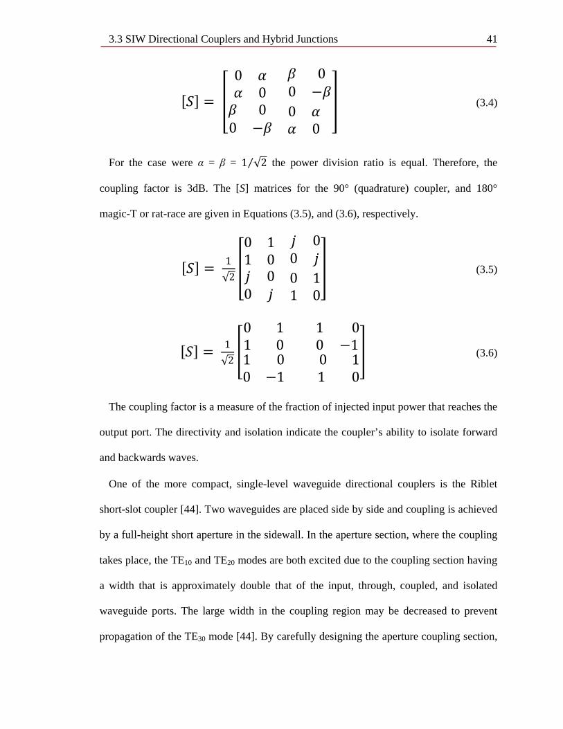
3.3 SIW Directional Couplers and Hybrid Junctions 41
[𝑆𝑆] = �
0 𝛼𝛼𝛼𝛼 0
𝑗𝑗 00 −𝑗𝑗
𝑗𝑗 00 −𝑗𝑗
0 𝛼𝛼𝛼𝛼 0
� (3.4)
For the case were α = β = 1 √2⁄ the power division ratio is equal. Therefore, the
coupling factor is 3dB. The [S] matrices for the 90° (quadrature) coupler, and 180°
magic-T or rat-race are given in Equations (3.5), and (3.6), respectively.
[𝑆𝑆] = 1√2�
0 11 0
𝑗𝑗 00 𝑗𝑗
𝑗𝑗 00 𝑗𝑗
0 11 0
� (3.5)
[𝑆𝑆] = 1√2�
0 11 0
1 00 −1
1 00 −1
0 1 1 0
� (3.6)
The coupling factor is a measure of the fraction of injected input power that reaches the
output port. The directivity and isolation indicate the coupler’s ability to isolate forward
and backwards waves.
One of the more compact, single-level waveguide directional couplers is the Riblet
short-slot coupler [44]. Two waveguides are placed side by side and coupling is achieved
by a full-height short aperture in the sidewall. In the aperture section, where the coupling
takes place, the TE10 and TE20 modes are both excited due to the coupling section having
a width that is approximately double that of the input, through, coupled, and isolated
waveguide ports. The large width in the coupling region may be decreased to prevent
propagation of the TE30 mode [44]. By carefully designing the aperture coupling section,
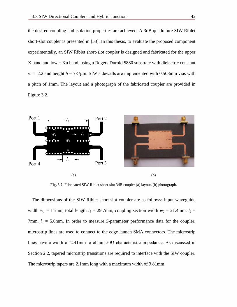
3.3 SIW Directional Couplers and Hybrid Junctions 42 the desired coupling and isolation properties are achieved. A 3dB quadrature SIW Riblet
short-slot coupler is presented in [53]. In this thesis, to evaluate the proposed component
experimentally, an SIW Riblet short-slot coupler is designed and fabricated for the upper
X band and lower Ku band, using a Rogers Duroid 5880 substrate with dielectric constant
εr = 2.2 and height h = 787μm. SIW sidewalls are implemented with 0.508mm vias with
a pitch of 1mm. The layout and a photograph of the fabricated coupler are provided in
Figure 3.2.
(a) (b)
Fig. 3.2 Fabricated SIW Riblet short-slot 3dB coupler (a) layout, (b) photograph.
The dimensions of the SIW Riblet short-slot coupler are as follows: input waveguide
width w1 = 11mm, total length l1 = 29.7mm, coupling section width w2 = 21.4mm, l2 =
7mm, l3 = 5.6mm. In order to measure S-parameter performance data for the coupler,
microstrip lines are used to connect to the edge launch SMA connectors. The microstrip
lines have a width of 2.41mm to obtain 50Ω characteristic impedance. As discussed in
Section 2.2, tapered microstrip transitions are required to interface with the SIW coupler.
The microstrip tapers are 2.1mm long with a maximum width of 3.81mm.
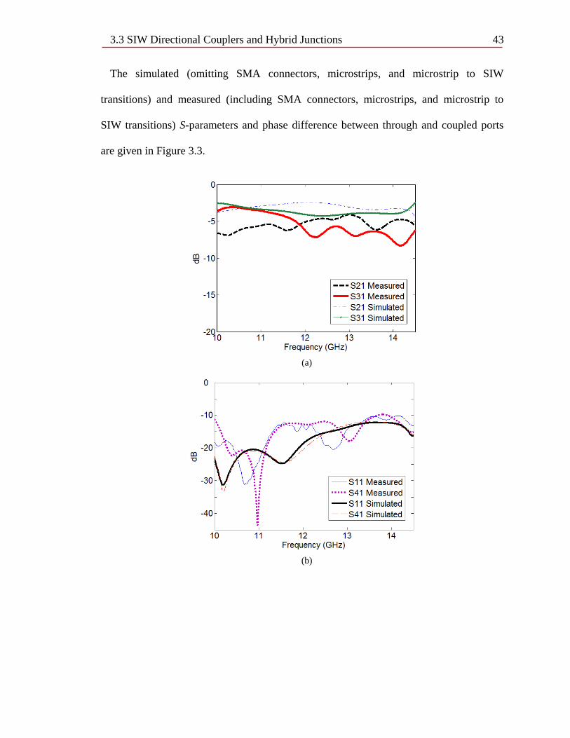
3.3 SIW Directional Couplers and Hybrid Junctions 43
The simulated (omitting SMA connectors, microstrips, and microstrip to SIW
transitions) and measured (including SMA connectors, microstrips, and microstrip to
SIW transitions) S-parameters and phase difference between through and coupled ports
are given in Figure 3.3.
(a)
(b)
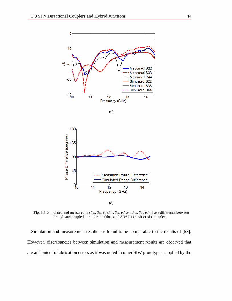
3.3 SIW Directional Couplers and Hybrid Junctions 44
(c)
(d)
Fig. 3.3 Simulated and measured (a) S21, S31, (b) S11, S41, (c) S22, S33, S44, (d) phase difference between through and coupled ports for the fabricated SIW Riblet short-slot coupler.
Simulation and measurement results are found to be comparable to the results of [53].
However, discrepancies between simulation and measurement results are observed that
are attributed to fabrication errors as it was noted in other SIW prototypes supplied by the
3.3 SIW Directional Couplers and Hybrid Junctions 45 PCB manufacturing company employed. As well, the effect of SMA connectors and
microstrip feed lines are not included in the coupler simulations.
Similar 3dB quadrature HMSIW and SIW couplers are presented in [16]. The results
achieved for the HMSIW coupler are somewhat better than those of the SIW coupler. The
authors include photographic evidence to demonstrate the overall size reduction achieved
by implementing the coupler with HMSIW technology.
In [18], the authors present another miniaturized narrow wall coupler using the T-
septum folded SIW interconnect. In this case, the reported bandwidth is approximately
3GHz, as opposed to the previously mentioned designs that show approximately 5GHz of
usable bandwidth. The authors continue their SIW coupler miniaturization attempts in
[18] by introducing a folded T-septum HMSIW coupler with two separate coupling
apertures. The operating bandwidth for the proposed ultra-miniature couplers is
approximately 4GHz in this work. Photographic evidence is provided in the reference to
demonstrate the extreme miniaturization that is achievable with this method.
The 180° 3dB SIW-based couplers are presented in [17]. The authors propose several
designs for both SIW and HMSIW-based couplers, operating in the C, X, Ka, and Ku
bands. The presented phase offsets are very large in comparison to the quadrature
hybrids. The special SIW hybrid ring and magic-T 180° couplers are presented in [19],
and [20], respectively. The hybrid ring of [19] is designed using the folded T-septum
SIW technology and has a small bandwidth for such a complex design. The SIW-based
magic-T of [20] has a reported bandwidth of nearly 5GHz with significantly improved
phase balance. However, the proposed magic-T is not a pure waveguide-based
component as it is a hybrid of SIW and microstrip elements.
46
3.4 Applications of SIW Components in Electronic Circuits and Systems
Several important SIW-based system components are reviewed in this Section. In [54],
an MMIC mixer module is fabricated in a 180nm gallium arsenide (GaAs) process. A
channel select filter is required at the radio frequency (RF) port of the mixer. In order to
incorporate an MMIC mixer into a microwave system, it must be mounted to a PCB to
connect to the other system components. The area of the proposed mixer PCB is 3cm x
3cm on the Rogers Duroid 5880 with dielectric constant of 2.2 and thickness of 250μm.
For an RF input power of -13dBm at 36.5GHz, with LO power of 9.13dBm at 38GHz a
conversion gain of 4dB is reported.
A low cost single-balanced mixer based on the Riblet short-slot SIW coupler and a pair
of diodes is presented in [53]. The authors achieve a 6.8dB conversion loss for a -10dBm
RF input and 8dBm 11.92GHz LO. This paper is significant as it demonstrates a design
methodology that allows microwave designers to implement a mixer with low cost off-
the-shelf components and a single-layer PCB layout technique. The introduction of the
SIW-based mixer marks a milestone in the development of fully integrated System-on-
Substrate (SoS) transceivers.
Another significant research effort is the development of a Low Temperature Co-fired
Ceramic (LTCC) MCM, presented in [31], that consists of an integrated SIW coupled
cavity filter and double-slot antenna. The 60GHz MCM receiver demonstrates the great
potential of SIW components for mass producing highly complex microwave systems at
relatively low cost in compact self-contained modules. The entire module, including the
integrated antenna measures only 22.5mm x 5.4mm x 0.3mm and operates from 58-
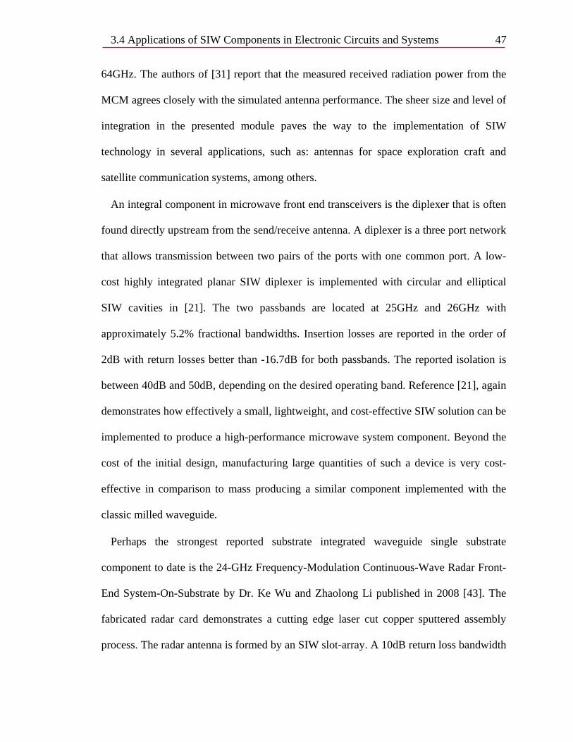
3.4 Applications of SIW Components in Electronic Circuits and Systems 47 64GHz. The authors of [31] report that the measured received radiation power from the
MCM agrees closely with the simulated antenna performance. The sheer size and level of
integration in the presented module paves the way to the implementation of SIW
technology in several applications, such as: antennas for space exploration craft and
satellite communication systems, among others.
An integral component in microwave front end transceivers is the diplexer that is often
found directly upstream from the send/receive antenna. A diplexer is a three port network
that allows transmission between two pairs of the ports with one common port. A low-
cost highly integrated planar SIW diplexer is implemented with circular and elliptical
SIW cavities in [21]. The two passbands are located at 25GHz and 26GHz with
approximately 5.2% fractional bandwidths. Insertion losses are reported in the order of
2dB with return losses better than -16.7dB for both passbands. The reported isolation is
between 40dB and 50dB, depending on the desired operating band. Reference [21], again
demonstrates how effectively a small, lightweight, and cost-effective SIW solution can be
implemented to produce a high-performance microwave system component. Beyond the
cost of the initial design, manufacturing large quantities of such a device is very cost-
effective in comparison to mass producing a similar component implemented with the
classic milled waveguide.
Perhaps the strongest reported substrate integrated waveguide single substrate
component to date is the 24-GHz Frequency-Modulation Continuous-Wave Radar Front-
End System-On-Substrate by Dr. Ke Wu and Zhaolong Li published in 2008 [43]. The
fabricated radar card demonstrates a cutting edge laser cut copper sputtered assembly
process. The radar antenna is formed by an SIW slot-array. A 10dB return loss bandwidth
3.4 Applications of SIW Components in Electronic Circuits and Systems 48 of approximately 650MHz, centered at 24GHz, is achieved. By developing the entire
receiver system in a substrate integrated platform, the complexity involved in connecting
MMIC components to the antenna architecture is avoided. The measured intermediate
frequency (IF) voltage spectrum, has a peak of approximately 4mV at 121.44kHz for a
2m target distance.
To complete this review chapter, two research efforts are presented that focus on
implementing the proposed SIW interconnects in high-frequency signaling systems with
time domain measurements. In [55], the authors propose a new hybrid SIW structure that
effectively provides designers with an additional baseband stripline transmission channel
buried inside the SIW. It is shown that the coupling from the TEM mode, of the baseband
channel, to the TE10 mode of the SIW is minimal. Over the design bandwidth, the
simulated coupling is observed to be less than -60dB between the stripline and dominant
waveguide mode. The proposed hybrid structure may be extended to multiple buried
striplines and provides a significant amount of substrate reuse due to the additional
channel bandwidth available. For the case of a single buried stripline, the SIW provides
full EMI shielding. Design methodology is presented for design of the SIW narrow wall
apertures required to route the stripline interconnects out of the SIW core. The simulated
eye diagrams present the potential for aggregate data rates exceeding 40Gbps in the
proposed hybrid structures.
In [56], the authors propose the first SIW interconnects to exploit the higher order
transverse electric modes to transmit parallel data through a single SIW interconnect. A
stripline to TE20 SIW balun transition is developed with aid from the author of this thesis.
The TEM mode of the stripline is matched to a double layer SIW section via a taper. The
3.4 Applications of SIW Components in Electronic Circuits and Systems 49 tapered stripline section terminates to a center ground plane in the double layer SIW
section of the balun. As the upper and lower cross-sectional TEM mode electric field
lines are equal in magnitude with opposing polarity, two TE10 SIW signals that are 180°
out of phase are generated in the double layer SIW section. At the output of the double
layer SIW, the center ground plane is continued along the direction of propagation. Two
microstrip lines on the outer copper layers serve as outputs with 180° phase difference.
The microstrips are connected to the double layer SIW section via tapers for the required
simultaneous mode and impedance match. At the input of the TE20 excited SIW, the
center ground plane of the balun is terminated and the microstrips are bent, or chamfered,
in opposite directions, to line up with maximum positive and negative broadside electric
field magnitude distribution points, for excitation of the TE20 mode, located halfway
between the SIW center and outer wall. The proposed balun is presented in Figure 3.4.
Fig. 3.4 Stripline to TE20 excited SIW balun.

50
3.5 Summary
In this Chapter, a survey of important SIW-based components like filters, cavities, and
couplers are presented. In addition, some of the applications of these key components in
microwave and mm-wave electronic circuits are reviewed, including oscillators, mixers,
radars, and high-speed signaling systems. An SIW 3dB Riblet short-slot coupler was
designed and fabricated. Simulation and measurement results are presented for the
coupler. Discrepancies between simulation and measurement data may be attributed to
fabrication errors as well as the effect of SMA connectors and microstrip feed lines which
are not modeled in the coupler simulations.

51
Chapter 4 Substrate Integrated Waveguide Power Dividers 4.1 Survey of Existing Power Divider Technology 4.1.1 Introduction to Power Dividers
Power dividers are passive microwave devices commonly used to route multiple copies
of a signal within a system. They can be designed as multi-port power dividers with
unequal power division ratios. This chapter focuses on three-port power dividers
featuring equal power division ratios where half the power (-3dB) of an input signal is
delivered to each of the two output ports. Alternatively, for a reciprocal structure, a
combining function may be realized with two input signals adding together at a single
output port.
Following the analysis provided in [44], consider the S-parameter matrix for a three-
port network, as shown in Equation (4.1).
[𝑆𝑆] = �𝑆𝑆11 𝑆𝑆12 𝑆𝑆13𝑆𝑆21 𝑆𝑆22 𝑆𝑆23𝑆𝑆31 𝑆𝑆32 𝑆𝑆33
� (4.1)
If the device is passive and does not contain any anisotropic materials such as ferrite,
the [S] matrix will be symmetrical across the diagonal implying the device is reciprocal.
For a symmetric [S] matrix, 𝑆𝑆𝑖𝑖𝑗𝑗 = 𝑆𝑆𝑗𝑗𝑖𝑖 . To ensure maximum power transmission is
realized, the device should be lossless and matched at all ports. If the device is matched at

4.1 Survey of Existing Power Divider Technology 52 all ports, there is no reflected power at any of the ports and the [S] matrix diagonal entries
are zero, 𝑆𝑆𝑖𝑖𝑖𝑖 = 0. The [S] matrix for a matched and reciprocal three-port device is given
in Equation (4.2).
[𝑆𝑆] = �0 𝑆𝑆12 𝑆𝑆13𝑆𝑆12 0 𝑆𝑆23𝑆𝑆13 𝑆𝑆23 0
� (4.2)
For the network to be lossless, the [S] matrix must be unitary for the laws of energy
conservation to be satisfied. The six conditions of Equation (4.3) must be satisfied.
|𝑆𝑆12|2 + |𝑆𝑆13|2 = 1 (4.3a)
|𝑆𝑆12|2 + |𝑆𝑆23|2 = 1 (4.3b)
|𝑆𝑆13|2 + |𝑆𝑆23|2 = 1 (4.3c)
𝑆𝑆13∗ 𝑆𝑆23 = 0 (4.3d)
𝑆𝑆23∗ 𝑆𝑆12 = 0 (4.3e)
𝑆𝑆12∗ 𝑆𝑆13 = 0 (4.3f)
In order to satisfy the conditions of Equations (4.3d-f), two of the three remaining [S]
matrix parameters (𝑆𝑆12, 𝑆𝑆13, 𝑆𝑆23) must be zero. Clearly this conflicts with Equations
(4.3a-c). Therefore, it is not possible to create a three-port power divider that is lossless,
reciprocal, and simultaneously matched at all ports. To design a physically realizable
three-port power divider, one of the conditions must be relaxed [44].

4.1 Survey of Existing Power Divider Technology 53 4.1.2 Implementation: Waveguide and SIW Power Dividers Commonly, waveguide and SIW three-port power dividers are designed as T-type
junctions. In fact, the T-junction power divider can be implemented in practically any
type of transmission line medium [44]. In the absence of transmission loss, the T-junction
is lossless. In the classic milled waveguides it is common to see both E-plane and H-
plane T-junction power dividers. As the SIW interconnects are fabricated in planar
substrates, the H-plane T-junctions and Y-junctions, as shown in Figure 4.1, are mostly
used [2]. The T-junction and Y-junction SIW power dividers are investigated in detail in
[22, 48]. The Y-junction is in fact a bifurcated waveguide fed by a symmetrical step
junction [22]. The magnitude of the electric field distribution for the Y-junction SIW
power divider is shown in Figure 4.2, with (a) excitation at port 1, and (b) excitation at
port 2, or 3.
(a) (b)
Fig. 4.1 SIW three-port power divider (a) Y-junction, (b) T-junction.
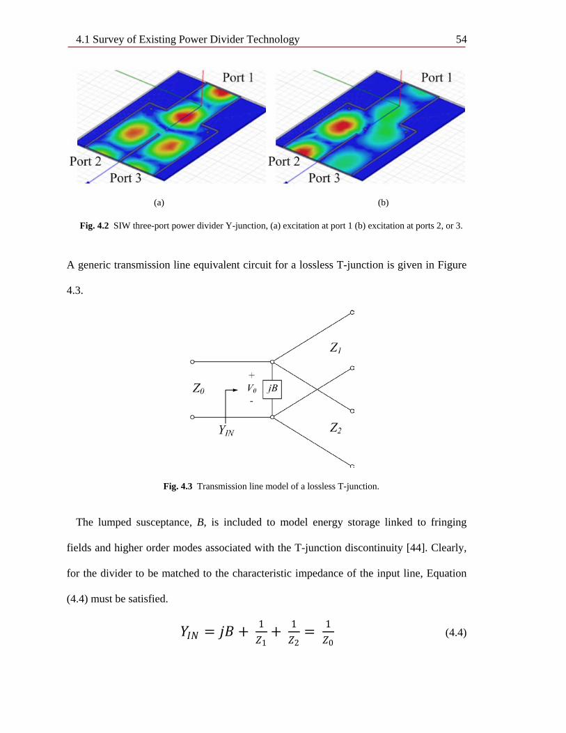
4.1 Survey of Existing Power Divider Technology 54
(a) (b)
Fig. 4.2 SIW three-port power divider Y-junction, (a) excitation at port 1 (b) excitation at ports 2, or 3.
A generic transmission line equivalent circuit for a lossless T-junction is given in Figure
4.3.
Fig. 4.3 Transmission line model of a lossless T-junction.
The lumped susceptance, B, is included to model energy storage linked to fringing
fields and higher order modes associated with the T-junction discontinuity [44]. Clearly,
for the divider to be matched to the characteristic impedance of the input line, Equation
(4.4) must be satisfied.
𝑌𝑌𝐼𝐼𝐼𝐼 = 𝑗𝑗𝐵𝐵 + 1𝑍𝑍1
+ 1𝑍𝑍2
= 1𝑍𝑍0
(4.4)

4.1 Survey of Existing Power Divider Technology 55
In waveguide T-junctions, the susceptance, B, is non-zero and is often tuned out with
an inductive post placed at the junction. The inductive post tuning method is utilized in
the work of [48]. From a fabrication standpoint, inductive posts, or vias, are much easier
to embed in the SIW interconnects compared to the classic milled metallic waveguides.
The T-junction and Y-junction power dividers lack isolation between the output ports,
as can be observed in Figure 4.2. If any mismatch is present at one of the output ports, the
reflected power is coupled to the adjacent port. Depending on the application, isolation
between output ports may be required. In order to improve port isolation Wilikinson
power dividers were introduced by J. Wilkinson in 1960 [57]. Section 4.1.3 reviews the
microstrip and stripline Wilkinson power dividers that possess the required isolation
characteristic.
4.1.3 Implementation: Microstrip and Stripline Wilkinson Power Dividers
Wilkinson found an elegant solution to implement a power divider with output port
isolation and capable of lossless transmission, provided the output ports are matched. A
resistive network is utilized to dissipate the reflected power from the output ports. As a
Wilkinson power divider requires the addition of a resistor in the power division section,
it is most commonly implemented in the microstrip and stripline transmission line
mediums. The transmission line model for the Wilkinson power divider is given in Figure
4.4.
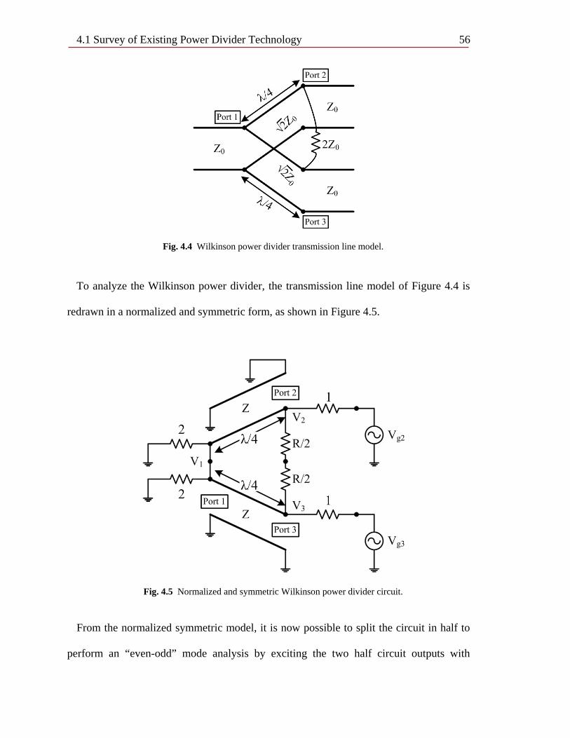
4.1 Survey of Existing Power Divider Technology 56
Fig. 4.4 Wilkinson power divider transmission line model.
To analyze the Wilkinson power divider, the transmission line model of Figure 4.4 is
redrawn in a normalized and symmetric form, as shown in Figure 4.5.
Fig. 4.5 Normalized and symmetric Wilkinson power divider circuit.
From the normalized symmetric model, it is now possible to split the circuit in half to
perform an “even-odd” mode analysis by exciting the two half circuit outputs with
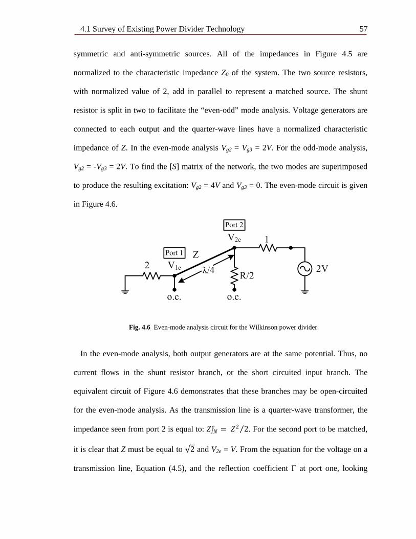
4.1 Survey of Existing Power Divider Technology 57 symmetric and anti-symmetric sources. All of the impedances in Figure 4.5 are
normalized to the characteristic impedance Z0 of the system. The two source resistors,
with normalized value of 2, add in parallel to represent a matched source. The shunt
resistor is split in two to facilitate the “even-odd” mode analysis. Voltage generators are
connected to each output and the quarter-wave lines have a normalized characteristic
impedance of Z. In the even-mode analysis Vg2 = Vg3 = 2V. For the odd-mode analysis,
Vg2 = -Vg3 = 2V. To find the [S] matrix of the network, the two modes are superimposed
to produce the resulting excitation: Vg2 = 4V and Vg3 = 0. The even-mode circuit is given
in Figure 4.6.
Fig. 4.6 Even-mode analysis circuit for the Wilkinson power divider.
In the even-mode analysis, both output generators are at the same potential. Thus, no
current flows in the shunt resistor branch, or the short circuited input branch. The
equivalent circuit of Figure 4.6 demonstrates that these branches may be open-circuited
for the even-mode analysis. As the transmission line is a quarter-wave transformer, the
impedance seen from port 2 is equal to: 𝑍𝑍𝐼𝐼𝐼𝐼𝑒𝑒 = 𝑍𝑍2 2⁄ . For the second port to be matched,
it is clear that Z must be equal to √2 and V2e = V. From the equation for the voltage on a
transmission line, Equation (4.5), and the reflection coefficient Γ at port one, looking
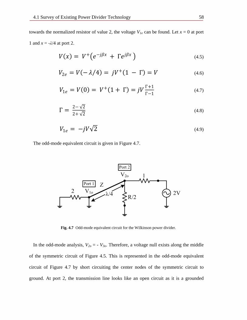
4.1 Survey of Existing Power Divider Technology 58 towards the normalized resistor of value 2, the voltage V1e can be found. Let x = 0 at port
1 and x = -λ/4 at port 2.
𝑉𝑉(𝑥𝑥) = 𝑉𝑉+�𝑒𝑒−𝑗𝑗𝑗𝑗𝑥𝑥 + Γ𝑒𝑒𝑗𝑗𝑗𝑗𝑥𝑥 � (4.5)
𝑉𝑉2𝑒𝑒 = 𝑉𝑉(−𝜆𝜆 4⁄ ) = 𝑗𝑗𝑉𝑉+(1 − Γ) = 𝑉𝑉 (4.6)
𝑉𝑉1𝑒𝑒 = 𝑉𝑉(0) = 𝑉𝑉+(1 + Γ) = 𝑗𝑗𝑉𝑉 Γ+1Γ−1
(4.7)
Γ = 2− √22+ √2
(4.8)
𝑉𝑉1𝑒𝑒 = −𝑗𝑗𝑉𝑉√2 (4.9)
The odd-mode equivalent circuit is given in Figure 4.7.
Fig. 4.7 Odd-mode equivalent circuit for the Wilkinson power divider.
In the odd-mode analysis, V2o = - V3o. Therefore, a voltage null exists along the middle
of the symmetric circuit of Figure 4.5. This is represented in the odd-mode equivalent
circuit of Figure 4.7 by short circuiting the center nodes of the symmetric circuit to
ground. At port 2, the transmission line looks like an open circuit as it is a grounded
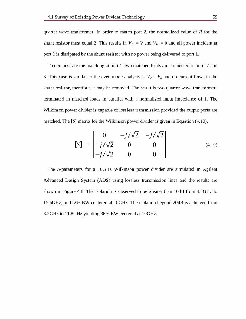
4.1 Survey of Existing Power Divider Technology 59 quarter-wave transformer. In order to match port 2, the normalized value of R for the
shunt resistor must equal 2. This results in V2o = V and V1o = 0 and all power incident at
port 2 is dissipated by the shunt resistor with no power being delivered to port 1.
To demonstrate the matching at port 1, two matched loads are connected to ports 2 and
3. This case is similar to the even mode analysis as V2 = V3 and no current flows in the
shunt resistor, therefore, it may be removed. The result is two quarter-wave transformers
terminated in matched loads in parallel with a normalized input impedance of 1. The
Wilkinson power divider is capable of lossless transmission provided the output ports are
matched. The [S] matrix for the Wilkinson power divider is given in Equation (4.10).
[𝑆𝑆] = �0 −𝑗𝑗 √2⁄ −𝑗𝑗 √2⁄
−𝑗𝑗 √2⁄ 0 0−𝑗𝑗 √2⁄ 0 0
� (4.10)
The S-parameters for a 10GHz Wilkinson power divider are simulated in Agilent
Advanced Design System (ADS) using lossless transmission lines and the results are
shown in Figure 4.8. The isolation is observed to be greater than 10dB from 4.4GHz to
15.6GHz, or 112% BW centered at 10GHz. The isolation beyond 20dB is achieved from
8.2GHz to 11.8GHz yielding 36% BW centered at 10GHz.
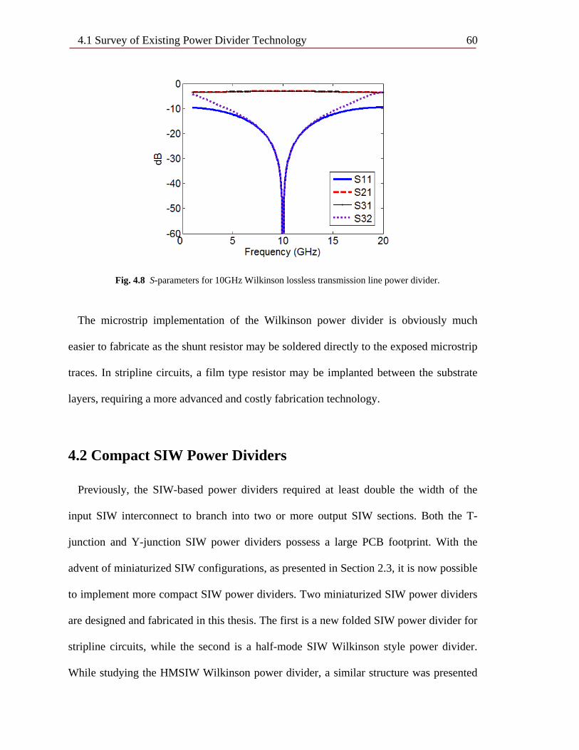
4.1 Survey of Existing Power Divider Technology 60
Fig. 4.8 S-parameters for 10GHz Wilkinson lossless transmission line power divider.
The microstrip implementation of the Wilkinson power divider is obviously much
easier to fabricate as the shunt resistor may be soldered directly to the exposed microstrip
traces. In stripline circuits, a film type resistor may be implanted between the substrate
layers, requiring a more advanced and costly fabrication technology.
4.2 Compact SIW Power Dividers
Previously, the SIW-based power dividers required at least double the width of the
input SIW interconnect to branch into two or more output SIW sections. Both the T-
junction and Y-junction SIW power dividers possess a large PCB footprint. With the
advent of miniaturized SIW configurations, as presented in Section 2.3, it is now possible
to implement more compact SIW power dividers. Two miniaturized SIW power dividers
are designed and fabricated in this thesis. The first is a new folded SIW power divider for
stripline circuits, while the second is a half-mode SIW Wilkinson style power divider.
While studying the HMSIW Wilkinson power divider, a similar structure was presented
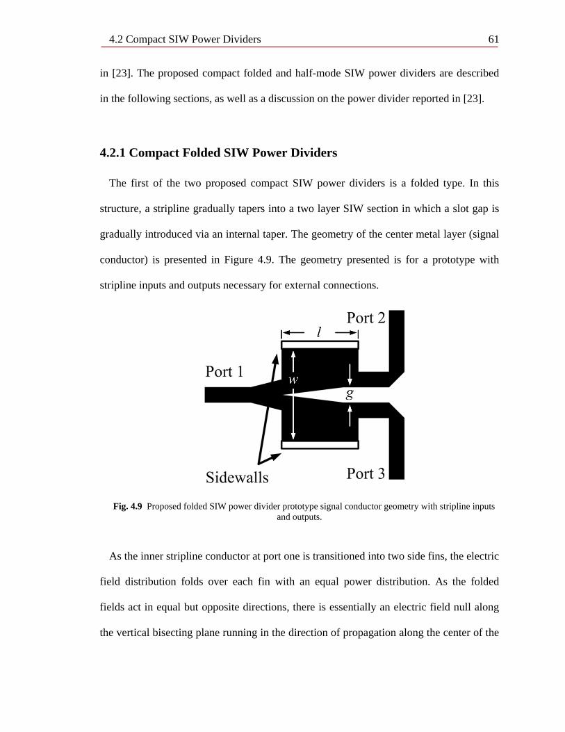
4.2 Compact SIW Power Dividers 61 in [23]. The proposed compact folded and half-mode SIW power dividers are described
in the following sections, as well as a discussion on the power divider reported in [23].
4.2.1 Compact Folded SIW Power Dividers
The first of the two proposed compact SIW power dividers is a folded type. In this
structure, a stripline gradually tapers into a two layer SIW section in which a slot gap is
gradually introduced via an internal taper. The geometry of the center metal layer (signal
conductor) is presented in Figure 4.9. The geometry presented is for a prototype with
stripline inputs and outputs necessary for external connections.
Fig. 4.9 Proposed folded SIW power divider prototype signal conductor geometry with stripline inputs and outputs.
As the inner stripline conductor at port one is transitioned into two side fins, the electric
field distribution folds over each fin with an equal power distribution. As the folded
fields act in equal but opposite directions, there is essentially an electric field null along
the vertical bisecting plane running in the direction of propagation along the center of the
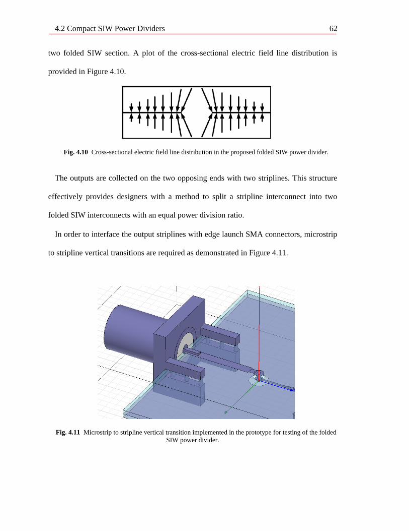
4.2 Compact SIW Power Dividers 62 two folded SIW section. A plot of the cross-sectional electric field line distribution is
provided in Figure 4.10.
Fig. 4.10 Cross-sectional electric field line distribution in the proposed folded SIW power divider.
The outputs are collected on the two opposing ends with two striplines. This structure
effectively provides designers with a method to split a stripline interconnect into two
folded SIW interconnects with an equal power division ratio.
In order to interface the output striplines with edge launch SMA connectors, microstrip
to stripline vertical transitions are required as demonstrated in Figure 4.11.
Fig. 4.11 Microstrip to stripline vertical transition implemented in the prototype for testing of the folded SIW power divider.

4.2 Compact SIW Power Dividers 63
An optimal vertical interconnect between stripline and microstrip requires blind vias
which increases the cost of fabrication. In order to decrease fabrication costs, through-
plated vias are needed with ground plane apertures (via anti-pad). A short section of high-
impedance microstrip line is inserted between the microstrip and via pad to compensate
for the vertical microstrip to stripline transition as suggested in [58]. Due to fabrication
process restrictions, through-plated vias must be outfitted with copper annular rings if not
terminated in an outer conductor layer. The effect of the annular ring adds to the parasitic
effects produced by the through-plated via as studied in [59]. The ultimate structure with
microstrip to stripline via transitions is simulated in HFSS. The structure of the SMA
connectors is also included in the layout. The power divider section has a width, w =
11.2mm and length, l = 8mm, as shown in Figure 4.9. The gap width, g = 0.3mm. All
microstrip lines are 0.7mm wide and all striplines are 0.28mm wide. The microstrip to
stripline transitions are optimized in HFSS by parametric simulations. The simulated
structure is demonstrated in Figure 4.12. The substrate considered is Rogers 4350 with
dielectric constant of 3.48, total thickness of 1.016mm with center stripline layer
0.508mm from the top and bottom ground planes.
The simulated S-parameters are presented in Figure 4.13.
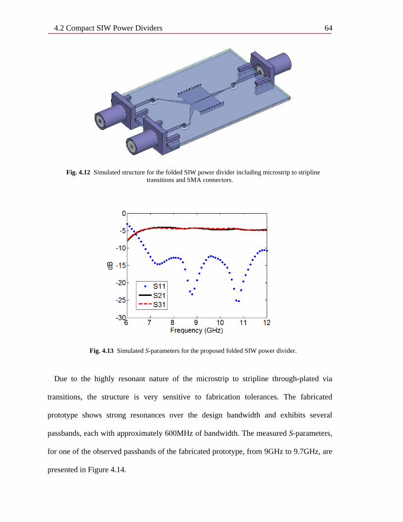
4.2 Compact SIW Power Dividers 64
Fig. 4.12 Simulated structure for the folded SIW power divider including microstrip to stripline
transitions and SMA connectors.
Fig. 4.13 Simulated S-parameters for the proposed folded SIW power divider.
Due to the highly resonant nature of the microstrip to stripline through-plated via
transitions, the structure is very sensitive to fabrication tolerances. The fabricated
prototype shows strong resonances over the design bandwidth and exhibits several
passbands, each with approximately 600MHz of bandwidth. The measured S-parameters,
for one of the observed passbands of the fabricated prototype, from 9GHz to 9.7GHz, are
presented in Figure 4.14.
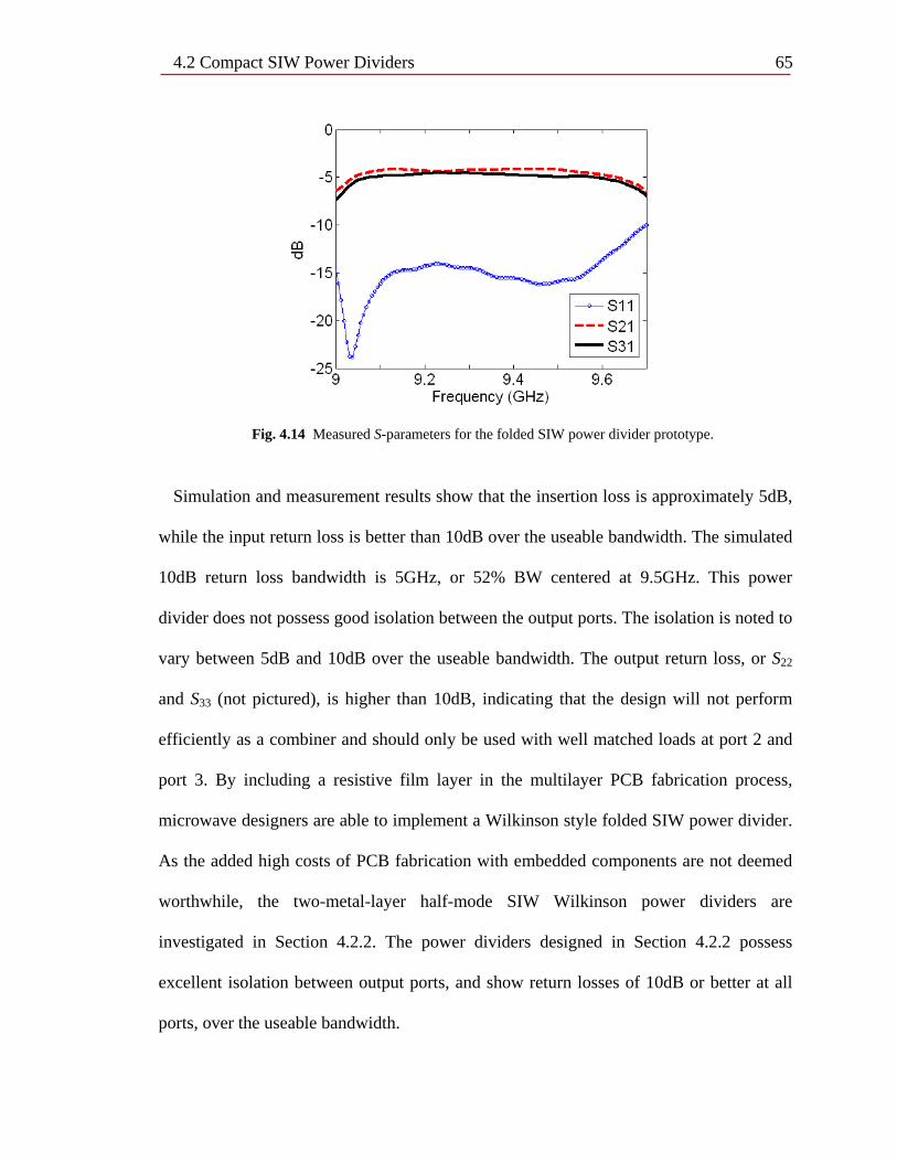
4.2 Compact SIW Power Dividers 65
Fig. 4.14 Measured S-parameters for the folded SIW power divider prototype.
Simulation and measurement results show that the insertion loss is approximately 5dB,
while the input return loss is better than 10dB over the useable bandwidth. The simulated
10dB return loss bandwidth is 5GHz, or 52% BW centered at 9.5GHz. This power
divider does not possess good isolation between the output ports. The isolation is noted to
vary between 5dB and 10dB over the useable bandwidth. The output return loss, or S22
and S33 (not pictured), is higher than 10dB, indicating that the design will not perform
efficiently as a combiner and should only be used with well matched loads at port 2 and
port 3. By including a resistive film layer in the multilayer PCB fabrication process,
microwave designers are able to implement a Wilkinson style folded SIW power divider.
As the added high costs of PCB fabrication with embedded components are not deemed
worthwhile, the two-metal-layer half-mode SIW Wilkinson power dividers are
investigated in Section 4.2.2. The power dividers designed in Section 4.2.2 possess
excellent isolation between output ports, and show return losses of 10dB or better at all
ports, over the useable bandwidth.
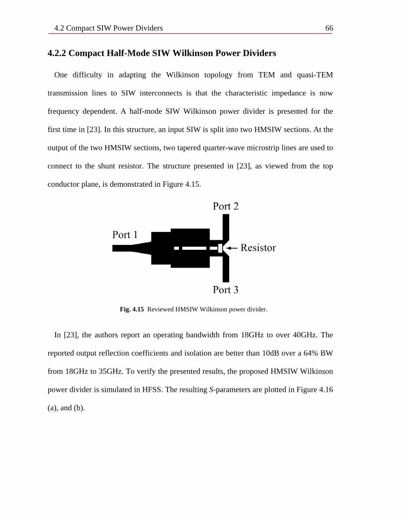
4.2 Compact SIW Power Dividers 66 4.2.2 Compact Half-Mode SIW Wilkinson Power Dividers
One difficulty in adapting the Wilkinson topology from TEM and quasi-TEM
transmission lines to SIW interconnects is that the characteristic impedance is now
frequency dependent. A half-mode SIW Wilkinson power divider is presented for the
first time in [23]. In this structure, an input SIW is split into two HMSIW sections. At the
output of the two HMSIW sections, two tapered quarter-wave microstrip lines are used to
connect to the shunt resistor. The structure presented in [23], as viewed from the top
conductor plane, is demonstrated in Figure 4.15.
Fig. 4.15 Reviewed HMSIW Wilkinson power divider.
In [23], the authors report an operating bandwidth from 18GHz to over 40GHz. The
reported output reflection coefficients and isolation are better than 10dB over a 64% BW
from 18GHz to 35GHz. To verify the presented results, the proposed HMSIW Wilkinson
power divider is simulated in HFSS. The resulting S-parameters are plotted in Figure 4.16
(a), and (b).
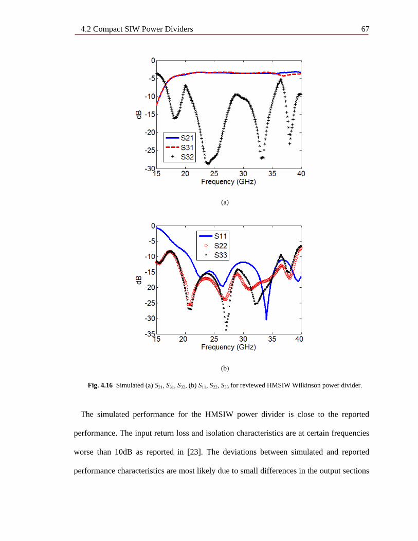
4.2 Compact SIW Power Dividers 67
(a)
(b)
Fig. 4.16 Simulated (a) S21, S31, S32, (b) S11, S22, S33 for reviewed HMSIW Wilkinson power divider.
The simulated performance for the HMSIW power divider is close to the reported
performance. The input return loss and isolation characteristics are at certain frequencies
worse than 10dB as reported in [23]. The deviations between simulated and reported
performance characteristics are most likely due to small differences in the output sections
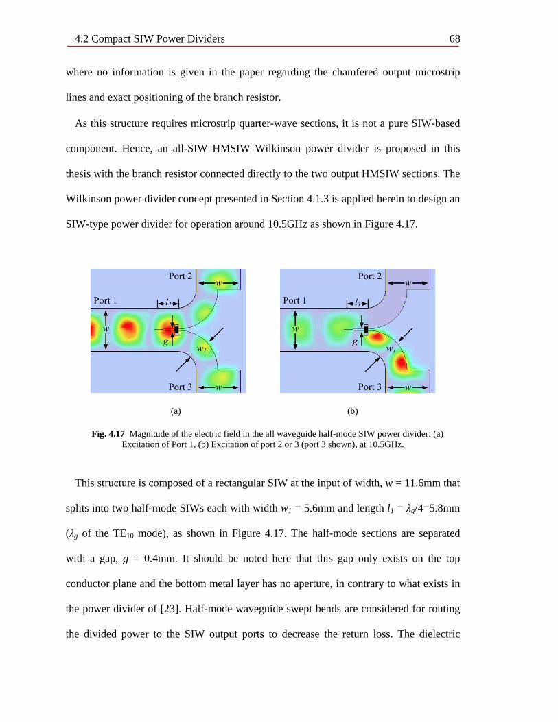
4.2 Compact SIW Power Dividers 68 where no information is given in the paper regarding the chamfered output microstrip
lines and exact positioning of the branch resistor.
As this structure requires microstrip quarter-wave sections, it is not a pure SIW-based
component. Hence, an all-SIW HMSIW Wilkinson power divider is proposed in this
thesis with the branch resistor connected directly to the two output HMSIW sections. The
Wilkinson power divider concept presented in Section 4.1.3 is applied herein to design an
SIW-type power divider for operation around 10.5GHz as shown in Figure 4.17.
(a) (b)
Fig. 4.17 Magnitude of the electric field in the all waveguide half-mode SIW power divider: (a) Excitation of Port 1, (b) Excitation of port 2 or 3 (port 3 shown), at 10.5GHz.
This structure is composed of a rectangular SIW at the input of width, w = 11.6mm that
splits into two half-mode SIWs each with width w1 = 5.6mm and length l1 = λg/4=5.8mm
(λg of the TE10 mode), as shown in Figure 4.17. The half-mode sections are separated
with a gap, g = 0.4mm. It should be noted here that this gap only exists on the top
conductor plane and the bottom metal layer has no aperture, in contrary to what exists in
the power divider of [23]. Half-mode waveguide swept bends are considered for routing
the divided power to the SIW output ports to decrease the return loss. The dielectric
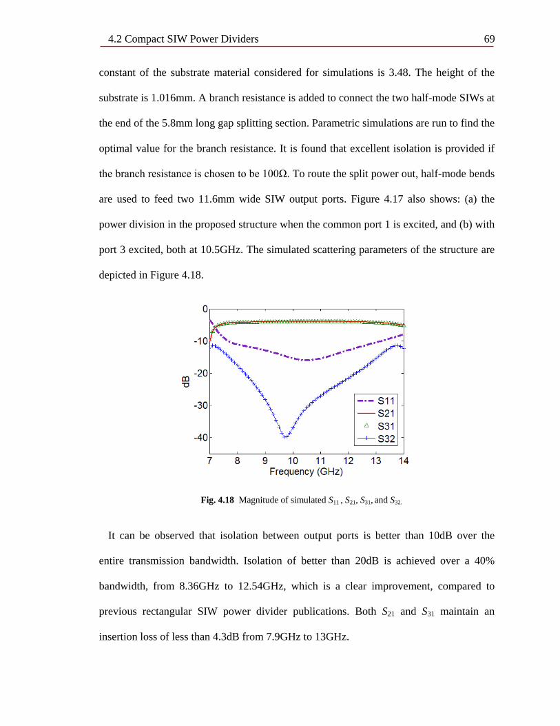
4.2 Compact SIW Power Dividers 69 constant of the substrate material considered for simulations is 3.48. The height of the
substrate is 1.016mm. A branch resistance is added to connect the two half-mode SIWs at
the end of the 5.8mm long gap splitting section. Parametric simulations are run to find the
optimal value for the branch resistance. It is found that excellent isolation is provided if
the branch resistance is chosen to be 100Ω. To route the split power out, half-mode bends
are used to feed two 11.6mm wide SIW output ports. Figure 4.17 also shows: (a) the
power division in the proposed structure when the common port 1 is excited, and (b) with
port 3 excited, both at 10.5GHz. The simulated scattering parameters of the structure are
depicted in Figure 4.18.
Fig. 4.18 Magnitude of simulated S11 , S21, S31, and S32.
It can be observed that isolation between output ports is better than 10dB over the
entire transmission bandwidth. Isolation of better than 20dB is achieved over a 40%
bandwidth, from 8.36GHz to 12.54GHz, which is a clear improvement, compared to
previous rectangular SIW power divider publications. Both S21 and S31 maintain an
insertion loss of less than 4.3dB from 7.9GHz to 13GHz.
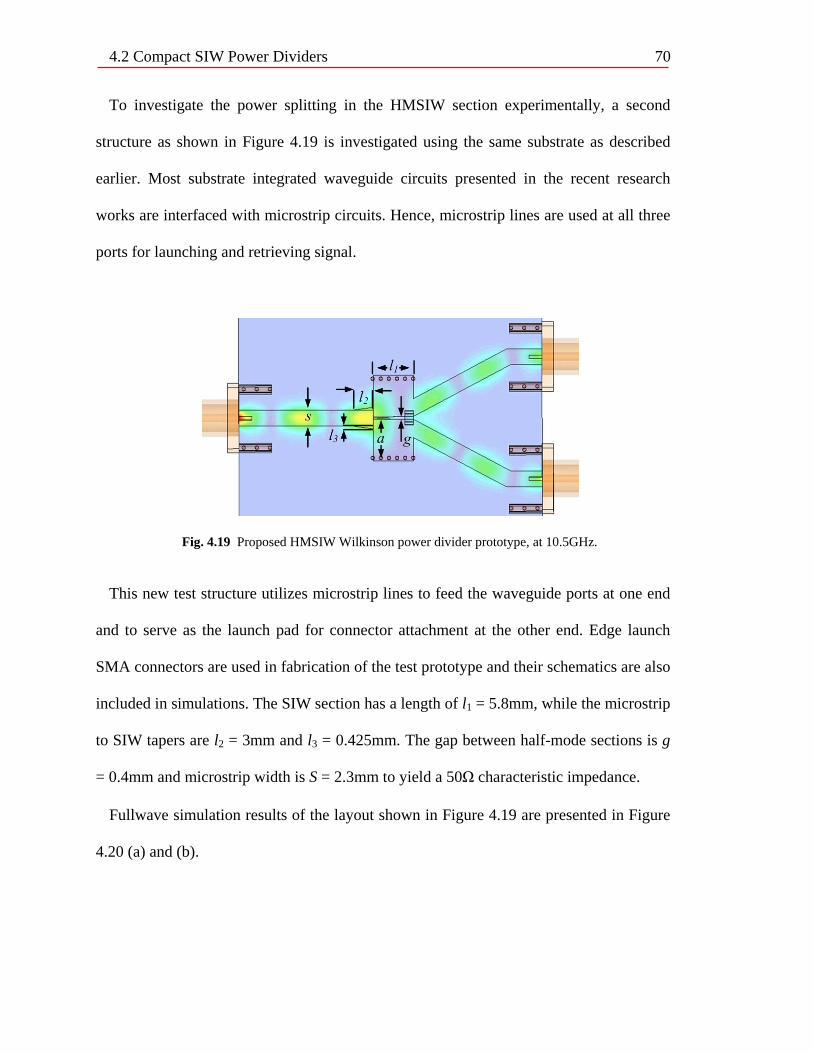
4.2 Compact SIW Power Dividers 70
To investigate the power splitting in the HMSIW section experimentally, a second
structure as shown in Figure 4.19 is investigated using the same substrate as described
earlier. Most substrate integrated waveguide circuits presented in the recent research
works are interfaced with microstrip circuits. Hence, microstrip lines are used at all three
ports for launching and retrieving signal.
Fig. 4.19 Proposed HMSIW Wilkinson power divider prototype, at 10.5GHz.
This new test structure utilizes microstrip lines to feed the waveguide ports at one end
and to serve as the launch pad for connector attachment at the other end. Edge launch
SMA connectors are used in fabrication of the test prototype and their schematics are also
included in simulations. The SIW section has a length of l1 = 5.8mm, while the microstrip
to SIW tapers are l2 = 3mm and l3 = 0.425mm. The gap between half-mode sections is g
= 0.4mm and microstrip width is S = 2.3mm to yield a 50Ω characteristic impedance.
Fullwave simulation results of the layout shown in Figure 4.19 are presented in Figure
4.20 (a) and (b).
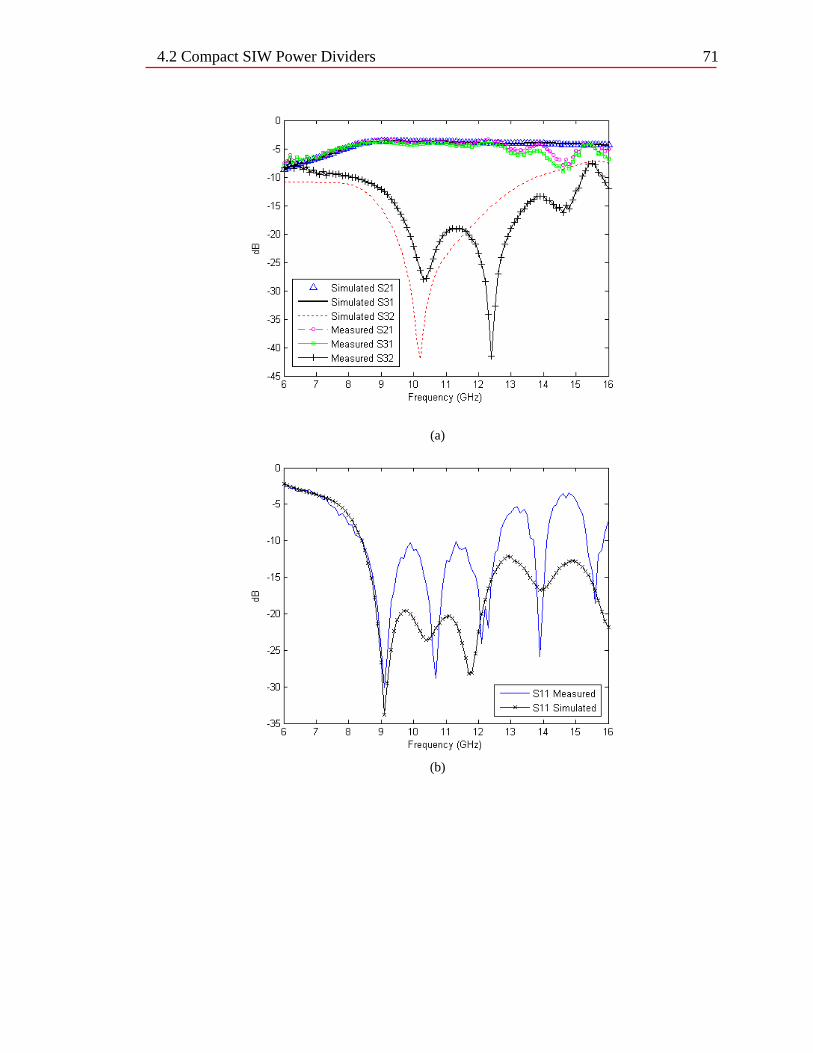
4.2 Compact SIW Power Dividers 71
(a)
(b)
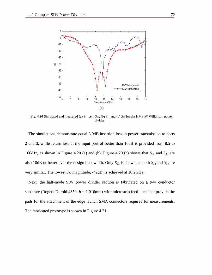
4.2 Compact SIW Power Dividers 72
(c)
Fig. 4.20 Simulated and measured (a) S21, S31, S32, (b) S11 and (c) S22 for the HMSIW Wilkinson power
divider.
The simulations demonstrate equal 3.9dB insertion loss in power transmission to ports
2 and 3, while return loss at the input port of better than 10dB is provided from 8.5 to
16GHz, as shown in Figure 4.20 (a) and (b). Figure 4.20 (c) shows that S22 and S33 are
also 10dB or better over the design bandwidth. Only S22 is shown, as both S22 and S33 are
very similar. The lowest S32 magnitude, -42dB, is achieved at 10.2GHz.
Next, the half-mode SIW power divider section is fabricated on a two conductor
substrate (Rogers Duroid 4350, h = 1.016mm) with microstrip feed lines that provide the
pads for the attachment of the edge launch SMA connectors required for measurements.
The fabricated prototype is shown in Figure 4.21.
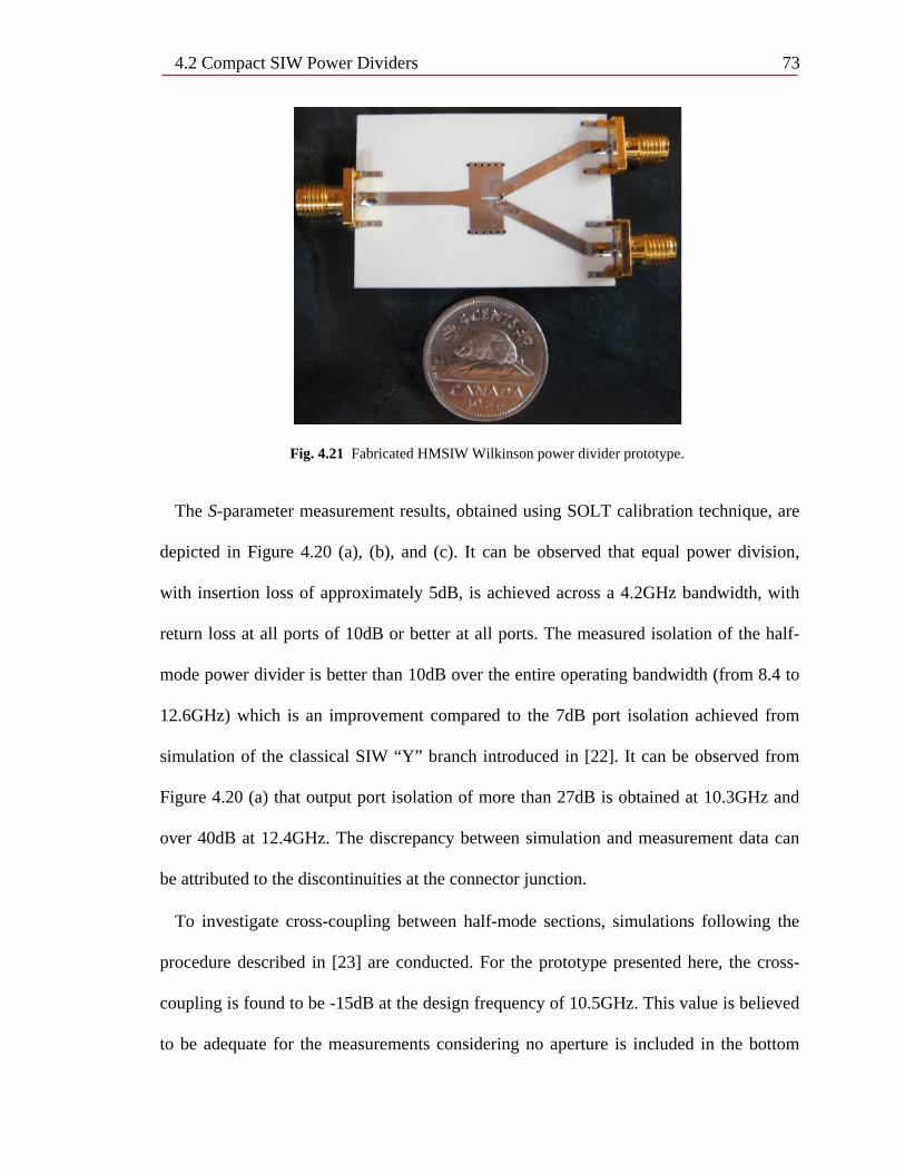
4.2 Compact SIW Power Dividers 73
Fig. 4.21 Fabricated HMSIW Wilkinson power divider prototype.
The S-parameter measurement results, obtained using SOLT calibration technique, are
depicted in Figure 4.20 (a), (b), and (c). It can be observed that equal power division,
with insertion loss of approximately 5dB, is achieved across a 4.2GHz bandwidth, with
return loss at all ports of 10dB or better at all ports. The measured isolation of the half-
mode power divider is better than 10dB over the entire operating bandwidth (from 8.4 to
12.6GHz) which is an improvement compared to the 7dB port isolation achieved from
simulation of the classical SIW “Y” branch introduced in [22]. It can be observed from
Figure 4.20 (a) that output port isolation of more than 27dB is obtained at 10.3GHz and
over 40dB at 12.4GHz. The discrepancy between simulation and measurement data can
be attributed to the discontinuities at the connector junction.
To investigate cross-coupling between half-mode sections, simulations following the
procedure described in [23] are conducted. For the prototype presented here, the cross-
coupling is found to be -15dB at the design frequency of 10.5GHz. This value is believed
to be adequate for the measurements considering no aperture is included in the bottom

4.2 Compact SIW Power Dividers 74 ground plane. Further reduction in cross coupling can be achieved by mirroring the top
gap on the bottom ground plane and increasing the gap width. This technique makes the
structure more prone to field leakage and electromagnetic interference and potentially
results in susceptibility problems.
4.3 Summary
Existing waveguide power dividers have been studied in this chapter. It is shown how
the Wilkinson power divider provides excellent isolation between output ports. Different
types of rectangular SIW power dividers are investigated and miniaturized power
dividers are designed. A folded SIW power divider is developed but it does not provide
adequate isolation and is not well matched at the output ports. Two improved half-mode
SIW Wilkinson power dividers are studied. The presented compact half-mode SIW
power dividers benefit from the excellent shielded transmission characteristics of the
SIW in the power splitting branch, unlike the previously published HMSIW Wilkinson
power divider. Two structures with waveguide and microstrip line feeds are simulated.
The simulations of the half-mode power divider with microstrip launchers demonstrate
similar results to those achieved with the all-waveguide half-mode SIW structure. A
prototype is fabricated to investigate the half-mode power divider with microstrip feed
lines. Measurement results demonstrate improved isolation characteristics in comparison
with the previously published literature on all SIW “Y” branch power dividers. A
passband of 4.2GHz, or 40% bandwidth centered at 10.5GHz, is measured. The measured
input return loss is less than 10dB, and the measured isolation was greater than 10dB over

4.3 Summary 75 the entire operating bandwidth. The maximum isolation is found to be over 40dB at
12.4GHz.
76
Chapter 5 Substrate Integrated Waveguide Cavity Resonators and Antennas 5.1 SIW Cavity Resonators, Antennas, and Oscillators 5.1.1 Introduction
SIW cavity resonators are introduced in Section 3.1.1, where it is shown how coupled
SIW cavity resonators are commonly implemented to design high-performance
microwave filters. In this section, two other applications of SIW cavity resonators are
discussed. SIW cavity resonators provide significantly enhanced performance, with a
high level of integration, in comparison to the previously available planar PCB
microwave resonators. The high quality factor of the waveguide-based cavity resonators
allows designers to implement microwave oscillators with very low phase noise as well
as compact high-gain antennas [26]. Fabricated SIW cavity oscillator prototypes are
showcased in Sections 5.1.2, and 5.2.2. SIW-cavity-based antenna design represents an
emerging research field that shows much promise for the availability of low-cost, fully-
integrated, high-performance antenna arrays and miniaturized flexible substrate antennas.
The development of SIW cavity resonators presents a significant achievement in
engineering. Among others, this new technology will find application in ultra-light
communication satellites, low payload spacecraft, un-manned drone aircraft, and high-
frequency sensors.

5.1 SIW Cavity Resonators, Antennas, and Oscillators 77 5.1.2 SIW Cavity Resonator Oscillators The first SIW cavity feedback oscillator is presented in [35]. A single discrete pHEMT
amplifier is tuned with a frequency-selective SIW-cavity-based feedback path. The
designed oscillator runs at 12.02GHz with a 20dB directional-coupler-based injection
locking stabilization scheme. The SIW cavity is used for both frequency selectivity and
feedback coupling in the amplifier. As the SIW components are inherently shorted at DC,
due to the through-via sidewalls, DC blocking capacitors are needed when connecting
them to any active devices requiring non-zero DC supply voltages. The design of the
proposed oscillator is done with a computer aided design (CAD) simulator. The loop gain
is set to 1dB with an electrical length tuned to provide a 0° phase shift. The authors
implement a fine tuning process (small stubs for loop phase adjustment) during the
fabrication of the oscillator to ensure the loop has the proper phase required for the
oscillation condition. The authors estimate the external quality factor of the oscillator
loop to be 178. The phase noise is calculated by Equation (5.1).
𝑃𝑃𝐼𝐼𝑡𝑡𝑖𝑖𝑠𝑠𝑒𝑒 = 𝑃𝑃𝑆𝑆𝑖𝑖𝑑𝑑𝑒𝑒𝑏𝑏𝑎𝑎𝑛𝑛𝑑𝑑 − 𝑃𝑃𝐶𝐶𝑎𝑎𝑟𝑟𝑟𝑟𝑖𝑖𝑒𝑒𝑟𝑟 − 10 log(𝑅𝑅𝐵𝐵𝐵𝐵) (5.1)
The authors report a measured sideband power (PSideband) of -43dBm at a 100kHz
separation from the carrier. The carrier power (PCarrier) is 0dBm and the spectrum
analyzer resolution bandwidth (RBW) is 1kHz. The phase noise for the oscillator in [35]
is calculated to be -73dBc/Hz.
Another significant advancement in the development of SIW-cavity-resonator
oscillators is presented in [26]. Measurement results are presented for multi-chip-module-
deposited (MCM-D) SIW cavities with resonance frequencies in the 58GHz to 75GHz
range. Due to the recent surge of attention for 60GHz applications and services such as

5.1 SIW Cavity Resonators, Antennas, and Oscillators 78 wireless local area networks (WLAN), and wireless personal area networks (WPAN), the
Interuniversity Microelectronics Center (IMEC) has developed a high-resistivity silicon
(HR-Si) integrated passive device (IPD) platform, including vias, to produce fully
integrated on-chip SIW cavities [26]. The proposed cavities present the possibility for on-
chip, high-gain, cavity-backed antennas, and low phase noise VCO applications. It is
proposed that the high quality factor of the SIW cavities could reduce the need for phase
locked loop (PLL) circuits, thereby reducing overall circuit size, power consumption,
cost, and time to market. The etched cavities have angled sidewalls. As a result, the
sidewall currents are forced to follow perturbed paths. Design equations are presented in
order to accurately predict the resonance frequency and quality factor of the etched
cavities. At the time of publication, the authors have only provided information for the
integrated cavities and not the full VCO design [26]. Further work for 60GHz SIW
antennas is presented in [60], where the authors stress the need to carefully design for
fabrication tolerances that can significantly shift the antenna operating frequency.
5.1.3 SIW Cavity Resonator Antennas
An ultra-wideband (UWB) HMSIW cavity-backed microstrip patch antenna is
presented in [61], that possesses the special characteristic of having multiple frequency
notches to prevent radiation of certain frequencies. The addition of the HMSIW cavity
and a coupling slot under the antenna feed line provides the required notch
characteristics.
In [62], the authors propose an SIW cavity dielectric resonator antenna where dielectric
resonators are adhered above slotted cavities to provide the radiating elements. The

5.1 SIW Cavity Resonators, Antennas, and Oscillators 79 proposed structure is suitable for parallel fed antenna arrays and achieves a very high
gain of approximately 10dB at the added cost of affixing the dielectric resonators.
A more cost effective SIW-fed circularly polarized single layer cavity-backed ring slot
antenna is presented in [32], while a similar SIW-fed cavity-backed patch antenna is
reported in [33]. The proposed antenna shows promise for integration in satellite antenna
arrays. It is lightweight and exhibits stabilized gain, and good return loss characteristic.
The prototype of [32] is implemented with microstrip feed although the structure can
clearly be fed by SIW interconnects in an all-SIW fed antenna array. The SIW circular
cavity reduces unwanted back-lobe radiation. A maximum gain of 5.5dB is achieved for
the antenna within the bandwidth of 8.875GHz to 10.875GHz [32].
5.2 Microstrip-Fed Circular SIW Cavity Resonators and Antennas
5.2.1 Design and Measurement of Microstrip-Fed Circular SIW Cavity Resonators
The objective of the design is to implement a circular cavity resonator using the SIW
technology with a Rogers substrate (Duroid 5880, εr = 2.2 and thickness of 0.787mm)
which resonates in the Ku band. Preliminary HFSS simulations were conducted for an
approximate structure, i.e. a closed cylinder with solid conductor walls, instead of the via
sidewall, with the diameter of 11mm. Simulations show that a resonance frequency
slightly above 14GHz for the TM010 mode is achieved [63]. For the SIW version of this
design, the solid sidewalls are replaced with a via fence composed of plated through
holes, with diameter of d = 0.508mm, and spacing of 10 degrees. In order to feed the

5.2 Microstrip-Fed Circular SIW Cavity Resonators and Antennas 80 resonator, a microstrip line terminated to a shorting via probe is used. For the purpose of
exciting the SIW-based structure, an area equivalent to the removal of six vias from the
sidewall is opened at the point of entry of the microstrip. In this manner, the SIW cavity’s
resonance characteristic is perturbed due to the opening in the sidewall, as well as the
creation of the folded slot around the microstrip and via pad. The layout of the resonator
and its design dimensions are presented in Figure 5.1. The matching of the resonator’s
input impedance to a 50Ω microstrip line with the width of W1 = 2.41mm, and length of
L1 = 7.5mm, is done via another narrow high-impedance section of microstrip line, with
the length L2, and width W2, which are tuned by parametric fullwave simulations to yield
the minimum S11 at the resonance frequency. It can be seen from fullwave simulations
that the resonance frequency and input resistance are also controlled by selecting the
appropriate geometrical sizing for Vd, d, Pd, Gd, and Cd parameters shown in Figure 1.
The ultimate geometric parameters that provide the best match, or highest return loss, at
the resonance frequency that is found to be of 16.13GHz are: L2 = 10.5mm, W2 = 0.8mm,
Vd = 0.508mm, Pd = 2mm, Gd = 4mm, Cd = 11mm. To reduce computational cost in the
simulations, the sidewalls of the cavity are set to perfect electric conductor vertical walls.
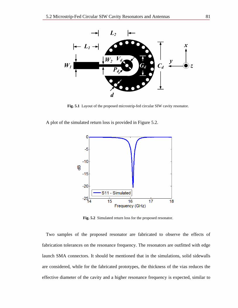
5.2 Microstrip-Fed Circular SIW Cavity Resonators and Antennas 81
Fig. 5.1 Layout of the proposed microstrip-fed circular SIW cavity resonator.
A plot of the simulated return loss is provided in Figure 5.2.
Fig. 5.2 Simulated return loss for the proposed resonator.
Two samples of the proposed resonator are fabricated to observe the effects of
fabrication tolerances on the resonance frequency. The resonators are outfitted with edge
launch SMA connectors. It should be mentioned that in the simulations, solid sidewalls
are considered, while for the fabricated prototypes, the thickness of the vias reduces the
effective diameter of the cavity and a higher resonance frequency is expected, similar to
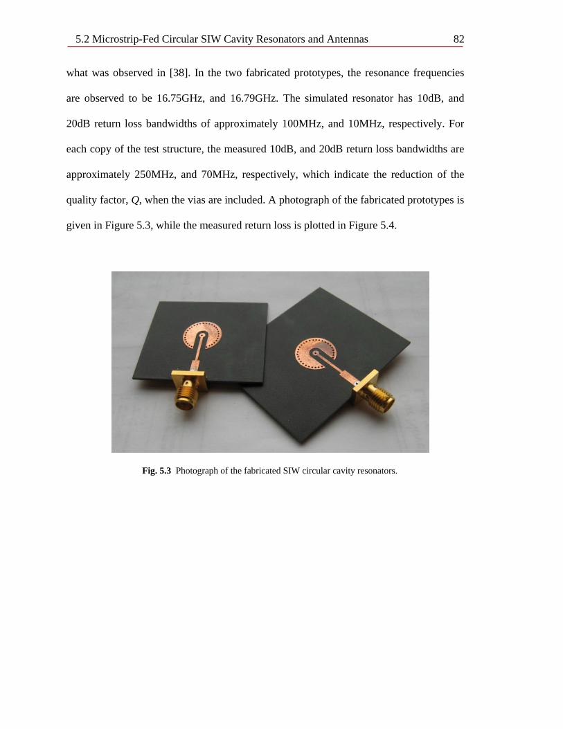
5.2 Microstrip-Fed Circular SIW Cavity Resonators and Antennas 82 what was observed in [38]. In the two fabricated prototypes, the resonance frequencies
are observed to be 16.75GHz, and 16.79GHz. The simulated resonator has 10dB, and
20dB return loss bandwidths of approximately 100MHz, and 10MHz, respectively. For
each copy of the test structure, the measured 10dB, and 20dB return loss bandwidths are
approximately 250MHz, and 70MHz, respectively, which indicate the reduction of the
quality factor, Q, when the vias are included. A photograph of the fabricated prototypes is
given in Figure 5.3, while the measured return loss is plotted in Figure 5.4.
Fig. 5.3 Photograph of the fabricated SIW circular cavity resonators.
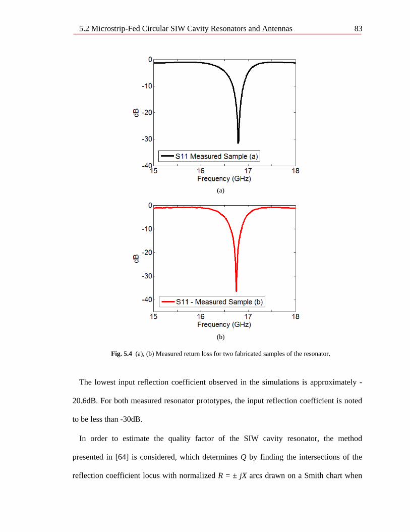
5.2 Microstrip-Fed Circular SIW Cavity Resonators and Antennas 83
(a)
(b)
Fig. 5.4 (a), (b) Measured return loss for two fabricated samples of the resonator.
The lowest input reflection coefficient observed in the simulations is approximately -
20.6dB. For both measured resonator prototypes, the input reflection coefficient is noted
to be less than -30dB.
In order to estimate the quality factor of the SIW cavity resonator, the method
presented in [64] is considered, which determines Q by finding the intersections of the
reflection coefficient locus with normalized R = ± jX arcs drawn on a Smith chart when
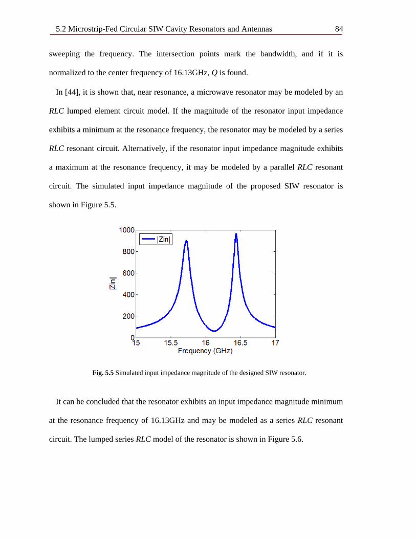
5.2 Microstrip-Fed Circular SIW Cavity Resonators and Antennas 84 sweeping the frequency. The intersection points mark the bandwidth, and if it is
normalized to the center frequency of 16.13GHz, Q is found.
In [44], it is shown that, near resonance, a microwave resonator may be modeled by an
RLC lumped element circuit model. If the magnitude of the resonator input impedance
exhibits a minimum at the resonance frequency, the resonator may be modeled by a series
RLC resonant circuit. Alternatively, if the resonator input impedance magnitude exhibits
a maximum at the resonance frequency, it may be modeled by a parallel RLC resonant
circuit. The simulated input impedance magnitude of the proposed SIW resonator is
shown in Figure 5.5.
Fig. 5.5 Simulated input impedance magnitude of the designed SIW resonator.
It can be concluded that the resonator exhibits an input impedance magnitude minimum
at the resonance frequency of 16.13GHz and may be modeled as a series RLC resonant
circuit. The lumped series RLC model of the resonator is shown in Figure 5.6.
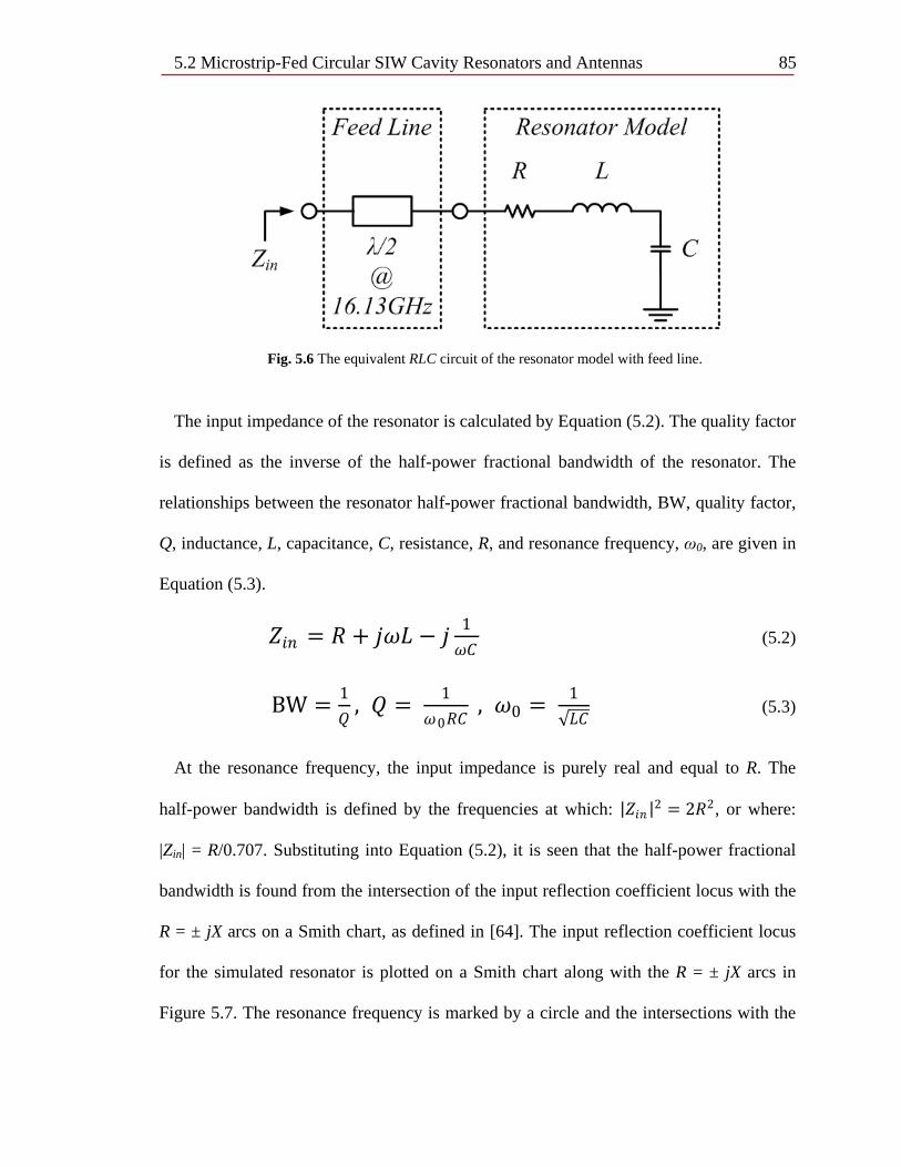
5.2 Microstrip-Fed Circular SIW Cavity Resonators and Antennas 85
Fig. 5.6 The equivalent RLC circuit of the resonator model with feed line.
The input impedance of the resonator is calculated by Equation (5.2). The quality factor
is defined as the inverse of the half-power fractional bandwidth of the resonator. The
relationships between the resonator half-power fractional bandwidth, BW, quality factor,
Q, inductance, L, capacitance, C, resistance, R, and resonance frequency, ω0, are given in
Equation (5.3).
𝑍𝑍𝑖𝑖𝑛𝑛 = 𝑅𝑅 + 𝑗𝑗𝑗𝑗𝑗𝑗 − 𝑗𝑗 1𝑗𝑗𝐶𝐶
(5.2)
BW = 1𝑄𝑄
, 𝑄𝑄 = 1𝑗𝑗0𝑅𝑅𝐶𝐶
, 𝑗𝑗0 = 1√𝑗𝑗𝐶𝐶
(5.3)
At the resonance frequency, the input impedance is purely real and equal to R. The
half-power bandwidth is defined by the frequencies at which: |𝑍𝑍𝑖𝑖𝑛𝑛 |2 = 2𝑅𝑅2, or where:
|Zin| = R/0.707. Substituting into Equation (5.2), it is seen that the half-power fractional
bandwidth is found from the intersection of the input reflection coefficient locus with the
R = ± jX arcs on a Smith chart, as defined in [64]. The input reflection coefficient locus
for the simulated resonator is plotted on a Smith chart along with the R = ± jX arcs in
Figure 5.7. The resonance frequency is marked by a circle and the intersections with the
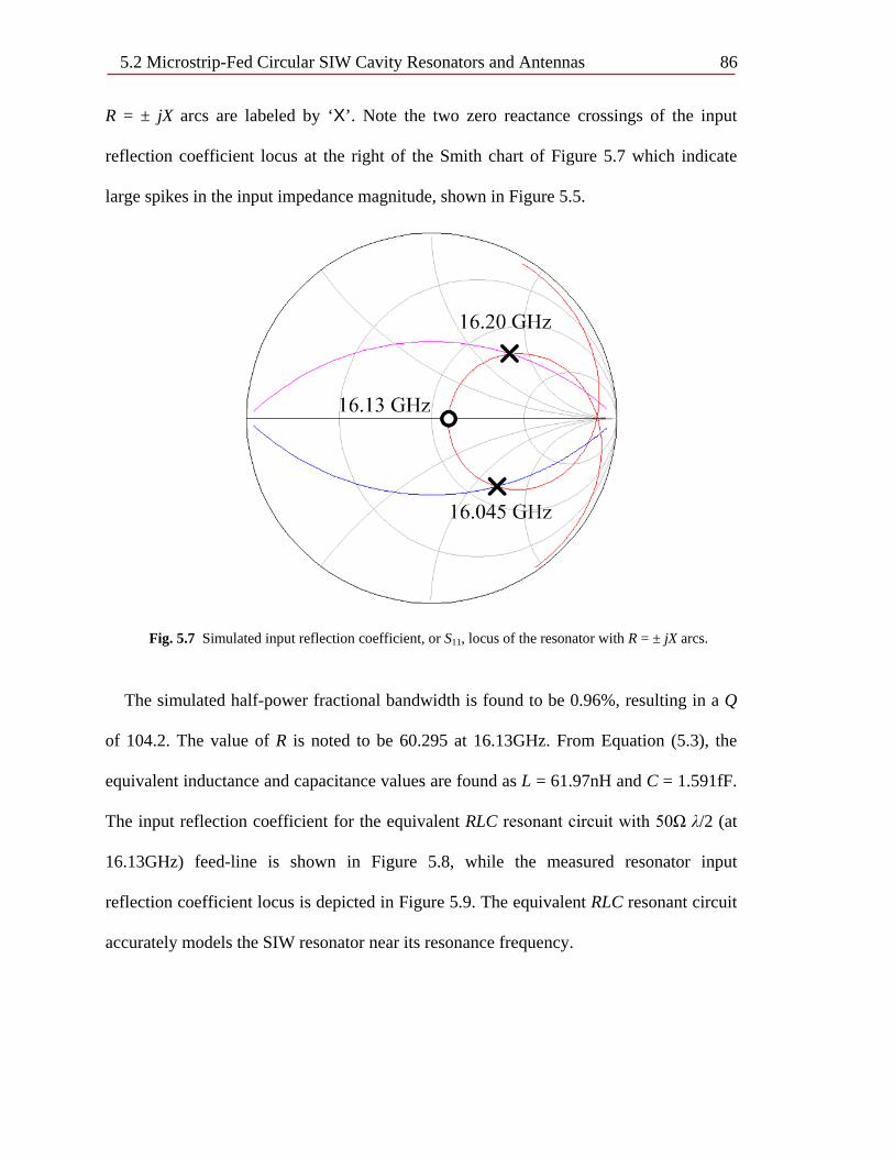
5.2 Microstrip-Fed Circular SIW Cavity Resonators and Antennas 86 R = ± jX arcs are labeled by ‘X’. Note the two zero reactance crossings of the input
reflection coefficient locus at the right of the Smith chart of Figure 5.7 which indicate
large spikes in the input impedance magnitude, shown in Figure 5.5.
Fig. 5.7 Simulated input reflection coefficient, or S11, locus of the resonator with R = ± jX arcs.
The simulated half-power fractional bandwidth is found to be 0.96%, resulting in a Q
of 104.2. The value of R is noted to be 60.295 at 16.13GHz. From Equation (5.3), the
equivalent inductance and capacitance values are found as L = 61.97nH and C = 1.591fF.
The input reflection coefficient for the equivalent RLC resonant circuit with 50Ω λ/2 (at
16.13GHz) feed-line is shown in Figure 5.8, while the measured resonator input
reflection coefficient locus is depicted in Figure 5.9. The equivalent RLC resonant circuit
accurately models the SIW resonator near its resonance frequency.
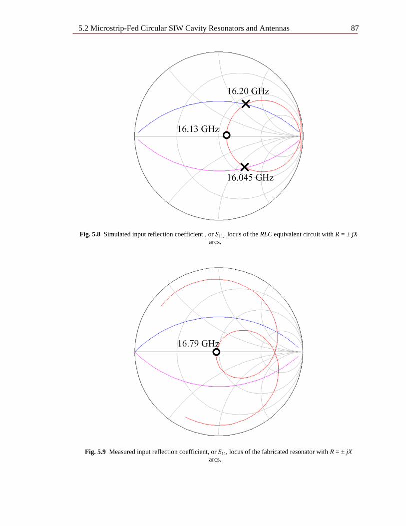
5.2 Microstrip-Fed Circular SIW Cavity Resonators and Antennas 87
Fig. 5.8 Simulated input reflection coefficient , or S11,, locus of the RLC equivalent circuit with R = ± jX arcs.
Fig. 5.9 Measured input reflection coefficient, or S11, locus of the fabricated resonator with R = ± jX arcs.
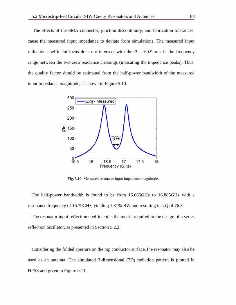
5.2 Microstrip-Fed Circular SIW Cavity Resonators and Antennas 88
The effects of the SMA connector, junction discontinuity, and fabrication tolerances,
cause the measured input impedance to deviate from simulations. The measured input
reflection coefficient locus does not intersect with the R = ± jX arcs in the frequency
range between the two zero reactance crossings (indicating the impedance peaks). Thus,
the quality factor should be estimated from the half-power bandwidth of the measured
input impedance magnitude, as shown in Figure 5.10.
Fig. 5.10 Measured resonator input impedance magnitude.
The half-power bandwidth is found to be from 16.665GHz to 16.885GHz with a
resonance frequency of 16.79GHz, yielding 1.31% BW and resulting in a Q of 76.3.
The resonator input reflection coefficient is the metric required in the design of a series
reflection oscillator, as presented in Section 5.2.2.
Considering the folded aperture on the top conductor surface, the resonator may also be
used as an antenna. The simulated 3-dimensional (3D) radiation pattern is plotted in
HFSS and given in Figure 5.11.

5.2 Microstrip-Fed Circular SIW Cavity Resonators and Antennas 89
Fig. 5.11 3-D radiation pattern for the proposed resonator antenna.
The maximum gain is observed to be approximately 5.5dB from simulations. The
simulated and measured xz-plane, and yz-plane, directive gain patterns are provided in
Figure 5.12 and Figure 5.13, respectively. One of the fabricated prototypes, sample b, is
tested in an anechoic chamber. The maximum measured gain is noted to be 7.76dB. A
slight deformation of the expected pattern is noted due to fabrication tolerances.
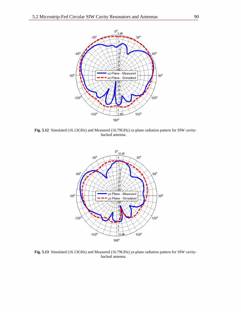
5.2 Microstrip-Fed Circular SIW Cavity Resonators and Antennas 90
Fig. 5.12 Simulated (16.13GHz) and Measured (16.79GHz) xz-plane radiation pattern for SIW cavity-backed antenna.
Fig. 5.13 Simulated (16.13GHz) and Measured (16.79GHz) yz-plane radiation pattern for SIW cavity-backed antenna.
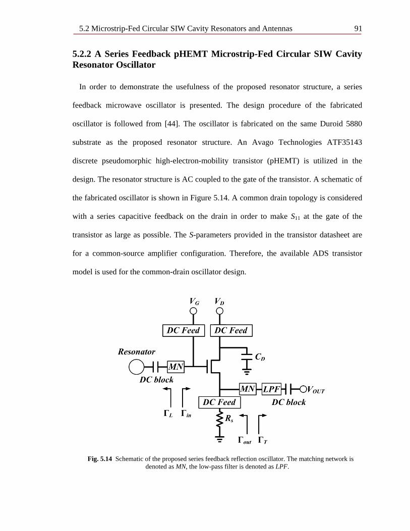
5.2 Microstrip-Fed Circular SIW Cavity Resonators and Antennas 91 5.2.2 A Series Feedback pHEMT Microstrip-Fed Circular SIW Cavity Resonator Oscillator
In order to demonstrate the usefulness of the proposed resonator structure, a series
feedback microwave oscillator is presented. The design procedure of the fabricated
oscillator is followed from [44]. The oscillator is fabricated on the same Duroid 5880
substrate as the proposed resonator structure. An Avago Technologies ATF35143
discrete pseudomorphic high-electron-mobility transistor (pHEMT) is utilized in the
design. The resonator structure is AC coupled to the gate of the transistor. A schematic of
the fabricated oscillator is shown in Figure 5.14. A common drain topology is considered
with a series capacitive feedback on the drain in order to make S11 at the gate of the
transistor as large as possible. The S-parameters provided in the transistor datasheet are
for a common-source amplifier configuration. Therefore, the available ADS transistor
model is used for the common-drain oscillator design.
Fig. 5.14 Schematic of the proposed series feedback reflection oscillator. The matching network is denoted as MN, the low-pass filter is denoted as LPF.

5.2 Microstrip-Fed Circular SIW Cavity Resonators and Antennas 92
The capacitive feedback connected between the drain and ground is required to create a
potentially unstable condition for the reflection coefficient looking into the gate of the
pHEMT at 16.13GHz. The transistor is biased with the intention of maximizing S11 at the
gate. A drain current of 32.2mA is found to provide the potentially unstable condition and
is achieved by selecting Rs = 20Ω, VD = 4V, and VG = 0.25V. The DC voltage at the
source output is 644mV.
In order to bias the transistor, a DC feed, or RF choke, is required to ensure the RF
signal at 16.13GHz does not leak from the circuit to the DC voltage sources. The RF
isolation between the transistor and DC supplies can be achieved using a high-impedance
open microstrip stub and transmission line, both with an electrical length of λ/4 at the
design frequency. The RF choke line width is set to 0.68mm to obtain 100Ω
characteristic impedance. A higher impedance line is implemented in the RF choke to
provide greater isolation between the oscillator and the DC supply. The DC voltage
supply is connected at the intersection between the line and stub which is effectively an
RF short-circuit. The RF short-circuit is transformed to an open-circuit, at the design
frequency, to provide the necessary isolation for the transistor’s operation. It is a standard
practice to implement the open λ /4 stub with a radial stub to increase the operating
bandwidth of the RF choke. In the fabricated layout, the radial stub length is 3.49mm.
The layout of the oscillator is shown in Figure 5.15.
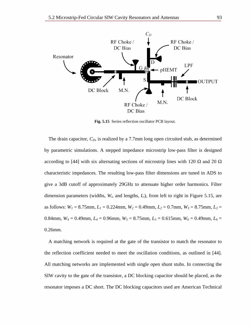
5.2 Microstrip-Fed Circular SIW Cavity Resonators and Antennas 93
Fig. 5.15 Series reflection oscillator PCB layout.
The drain capacitor, CD, is realized by a 7.7mm long open circuited stub, as determined
by parametric simulations. A stepped impedance microstrip low-pass filter is designed
according to [44] with six alternating sections of microstrip lines with 120 Ω and 20 Ω
characteristic impedances. The resulting low-pass filter dimensions are tuned in ADS to
give a 3dB cutoff of approximately 29GHz to attenuate higher order harmonics. Filter
dimension parameters (widths, Wi, and lengths, Li), from left to right in Figure 5.15, are
as follows: W1 = 8.75mm, L1 = 0.224mm, W2 = 0.49mm, L2 = 0.7mm, W3 = 8.75mm, L3 =
0.84mm, W4 = 0.49mm, L4 = 0.96mm, W5 = 8.75mm, L5 = 0.615mm, W6 = 0.49mm, L6 =
0.26mm.
A matching network is required at the gate of the transistor to match the resonator to
the reflection coefficient needed to meet the oscillation conditions, as outlined in [44].
All matching networks are implemented with single open shunt stubs. In connecting the
SIW cavity to the gate of the transistor, a DC blocking capacitor should be placed, as the
resonator imposes a DC short. The DC blocking capacitors used are American Technical

5.2 Microstrip-Fed Circular SIW Cavity Resonators and Antennas 94 Ceramics ATC100 series models with a capacitance of 100pF. The oscillator circuit
schematic with distributed components in ADS is given in Figure 5.16.
Fig. 5.16 ADS schematic for the series reflection oscillator.
The frequency of oscillation and output power are found by running the harmonic
balance simulator. The simulated output spectrum and time domain waveform are given
in Figure 5.17. The first harmonic is observed at 16.34GHz with an output power of
approximately 10dBm. The second harmonic is located at 32.67GHz with a signal power
of less than -63dBm. In [44], it is noted that a slight shift in oscillation frequency from
the resonator’s resonance frequency can be expected due to the non-linearity of the
transistor.
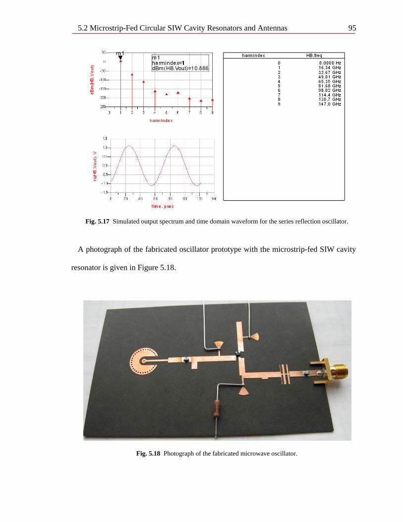
5.2 Microstrip-Fed Circular SIW Cavity Resonators and Antennas 95
Fig. 5.17 Simulated output spectrum and time domain waveform for the series reflection oscillator.
A photograph of the fabricated oscillator prototype with the microstrip-fed SIW cavity
resonator is given in Figure 5.18.
Fig. 5.18 Photograph of the fabricated microwave oscillator.
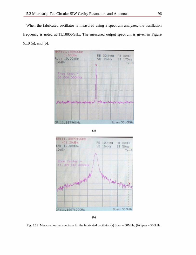
5.2 Microstrip-Fed Circular SIW Cavity Resonators and Antennas 96
When the fabricated oscillator is measured using a spectrum analyzer, the oscillation
frequency is noted at 11.18855GHz. The measured output spectrum is given in Figure
5.19 (a), and (b).
(a)
(b)
Fig. 5.19 Measured output spectrum for the fabricated oscillator (a) Span = 50MHz, (b) Span = 500kHz.

5.2 Microstrip-Fed Circular SIW Cavity Resonators and Antennas 97
The carrier power is observed to be approximately 1dBm with a sideband power of
approximately -43dBm at a 100kHz offset from the carrier. The resolution bandwidth of
the spectrum analyzer is set to 10kHz. By Equation (5.1) the phase noise is calculated to
be -82dBc/Hz. The fabricated series feedback microwave reflection oscillator
demonstrates a low phase noise considering the series feedback topology which is
generally less frequency selective than the parallel feedback topology [44].
In order to determine why the fabricated oscillator demonstrates free-running
oscillation near 11GHz instead of the design frequency of 16.13GHz, the ADS circuit is
analyzed. It is found that if the wires between the DC supplies and the radial stubs are
included in simulations, the first harmonic of the oscillator is shifted to approximately
24GHz. In order to investigate the performance of the RF chokes, the circuit of Figure
5.20 is considered. Figure 5.20 demonstrates the test circuit, used to simulate the effect of
adding the RF choke, at either of the gate, drain, or source terminals of the transistor for
(a) the original RF choke design, and (b) an improved RF choke design. In the test circuit
of Figure 5.20, both the DC supply and a 25cm long 24 gauge (0.5mm diameter) wire are
included in the simulations.
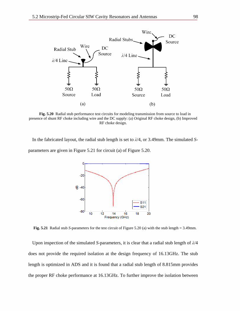
5.2 Microstrip-Fed Circular SIW Cavity Resonators and Antennas 98
Fig. 5.20 Radial stub performance test circuits for modeling transmission from source to load in presence of shunt RF choke including wire and the DC supply: (a) Original RF choke design, (b) Improved
RF choke design.
In the fabricated layout, the radial stub length is set to λ/4, or 3.49mm. The simulated S-
parameters are given in Figure 5.21 for circuit (a) of Figure 5.20.
Fig. 5.21 Radial stub S-parameters for the test circuit of Figure 5.20 (a) with the stub length = 3.49mm.
Upon inspection of the simulated S-parameters, it is clear that a radial stub length of λ/4
does not provide the required isolation at the design frequency of 16.13GHz. The stub
length is optimized in ADS and it is found that a radial stub length of 8.815mm provides
the proper RF choke performance at 16.13GHz. To further improve the isolation between
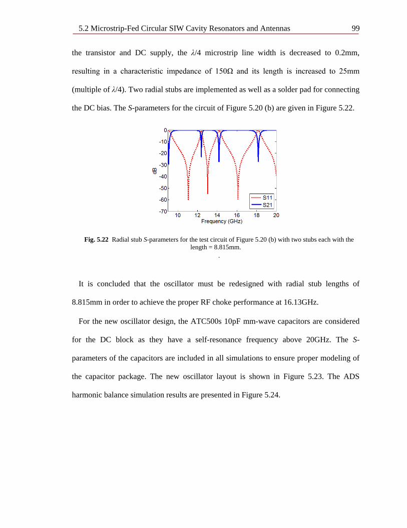
5.2 Microstrip-Fed Circular SIW Cavity Resonators and Antennas 99 the transistor and DC supply, the λ/4 microstrip line width is decreased to 0.2mm,
resulting in a characteristic impedance of 150Ω and its length is increased to 25mm
(multiple of λ/4). Two radial stubs are implemented as well as a solder pad for connecting
the DC bias. The S-parameters for the circuit of Figure 5.20 (b) are given in Figure 5.22.
Fig. 5.22 Radial stub S-parameters for the test circuit of Figure 5.20 (b) with two stubs each with the length = 8.815mm.
.
It is concluded that the oscillator must be redesigned with radial stub lengths of
8.815mm in order to achieve the proper RF choke performance at 16.13GHz.
For the new oscillator design, the ATC500s 10pF mm-wave capacitors are considered
for the DC block as they have a self-resonance frequency above 20GHz. The S-
parameters of the capacitors are included in all simulations to ensure proper modeling of
the capacitor package. The new oscillator layout is shown in Figure 5.23. The ADS
harmonic balance simulation results are presented in Figure 5.24.
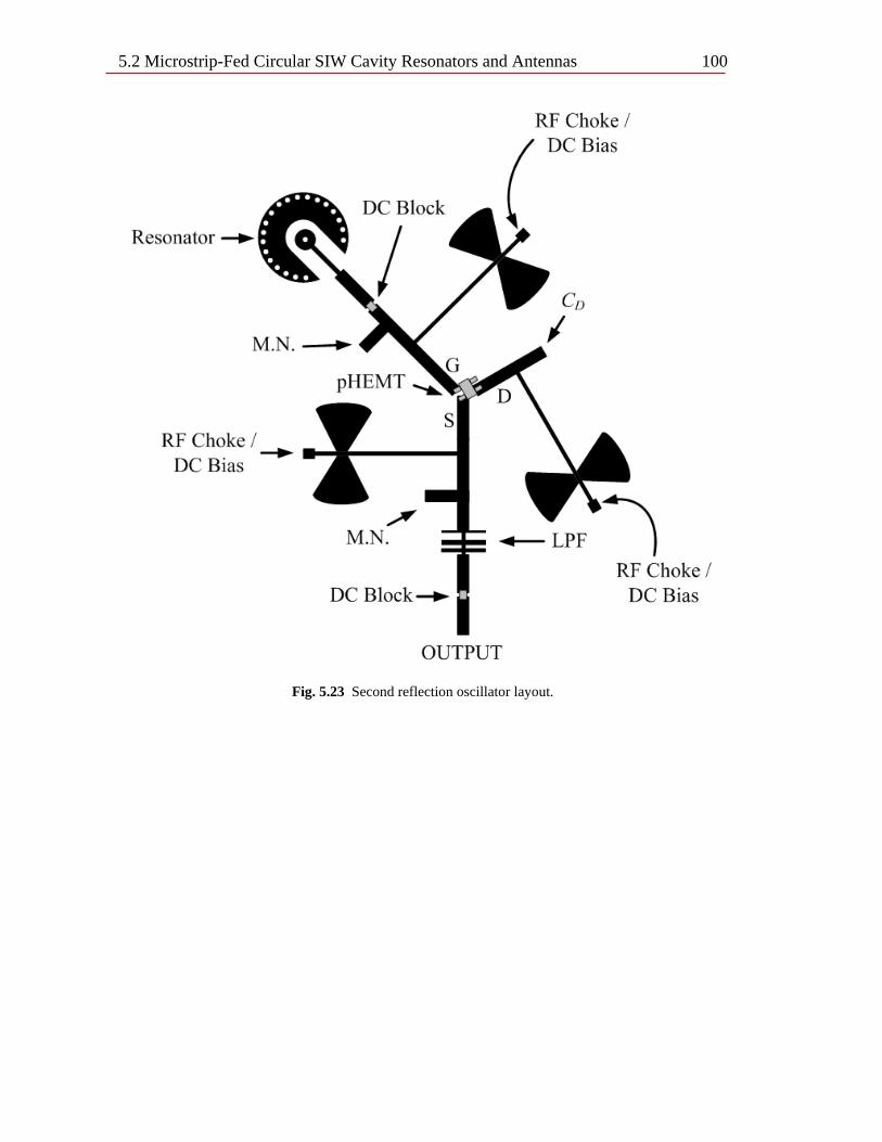
5.2 Microstrip-Fed Circular SIW Cavity Resonators and Antennas 100
Fig. 5.23 Second reflection oscillator layout.
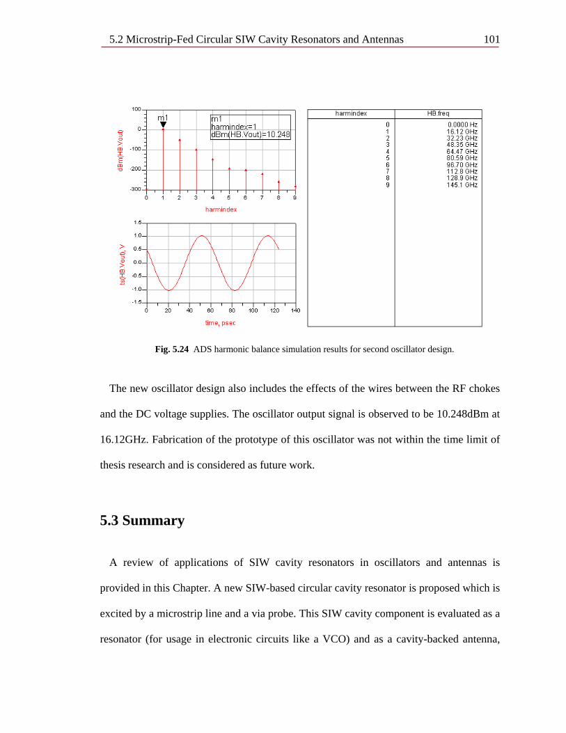
5.2 Microstrip-Fed Circular SIW Cavity Resonators and Antennas 101
Fig. 5.24 ADS harmonic balance simulation results for second oscillator design.
The new oscillator design also includes the effects of the wires between the RF chokes
and the DC voltage supplies. The oscillator output signal is observed to be 10.248dBm at
16.12GHz. Fabrication of the prototype of this oscillator was not within the time limit of
thesis research and is considered as future work.
5.3 Summary
A review of applications of SIW cavity resonators in oscillators and antennas is
provided in this Chapter. A new SIW-based circular cavity resonator is proposed which is
excited by a microstrip line and a via probe. This SIW cavity component is evaluated as a
resonator (for usage in electronic circuits like a VCO) and as a cavity-backed antenna,

5.3 Summary 102 due to the slot created on the top surface of the cavity for the feed line. The resonator has
a simulated gain of over 5dB at 16.13GHz when used as an antenna. The maximum
antenna gain at 16.79GHz is measured to be 7.76dB for the fabricated prototype. Also, at
the resonance frequency a very low reflection coefficient, better than -35dB, and a quality
factor of approximately 76.3 are measured for the SIW cavity. The measured radiation
patterns differ from the simulated patterns due to misalignments and errors in the
fabrication, which, along with other junction and connector discontinuities, contributed to
the differences between the measured and simulated input Q and impedance profiles.
A low phase noise microwave oscillator is designed and fabricated to demonstrate the
efficacy of the newly proposed resonator. The measured free-running oscillator frequency
was observed to be near 11GHz due to improperly sized radial stubs in the DC feed / RF
choke networks. A new layout is proposed and the simulated oscillation frequency is
observed to be 16.12GHz, with an output power of over 10dBm.
103
Chapter 6 Dispersion Equalization Techniques for Substrate Integrated Waveguide Interconnects 6.1 Waveguide Dispersion Equalization Techniques 6.1.1 Introduction
The SIW interconnect, which exhibits nearly identical propagation and dispersion
characteristics to those of a rectangular waveguide, has a highly non-linear propagation
constant close to cutoff. Thus, signals occupying the near cutoff region experience
distortion due the variation of propagation delay for different spectral components of the
signal. If the SIW is to become the standard in wideband analog or digital
interconnection, a thorough investigation of its dispersive properties and possible
equalization methods is in order.
In this Chapter, dispersion equalization of an SIW interconnect is investigated using
only passive RF components. Two methods based on the work of Pierce, Tang, and
Torgow in the late 1950s and early 1960s [36], [65-67], are investigated.
These techniques utilize a passive equalizer to achieve a more linear propagation
constant in a waveguide channel. The passive equalizer is a width-modulated waveguide
component, with a reflection coefficient phase designed to provide the delay required to
compensate for the non-linear propagation constant in the waveguide channel. The

6.1 Waveguide Dispersion Equalization Techniques 104 equalizer section is interfaced to the waveguide channel via a broadband circulator or
coupler, as outlined in Section 6.1.3. In this thesis, the design equations proposed by
Torgow, [36], are adapted to include the dielectric constant of the substrate integrated
environment. To the author’s knowledge, the first reflective substrate integrated
waveguide dispersion compensation systems are designed, fabricated, and measured in
the research conducted for this thesis.
6.1.2 Dispersion in Waveguides
The operating bandwidth of waveguide components is commonly considered to begin
after some guard band above the cutoff frequency of the waveguide. This practice is
necessary due to the non-linearity of the propagation constant close to cutoff that
contributes to significant distortion. A plot of the propagation constant β vs. frequency of
a typical SIW is shown in Figure 6.1. The light line, 𝑙𝑙 = 𝑗𝑗√𝜀𝜀𝜇𝜇, is also included to
demonstrate how the propagation constant in the SIW deviates from the ideal TEM
propagation.
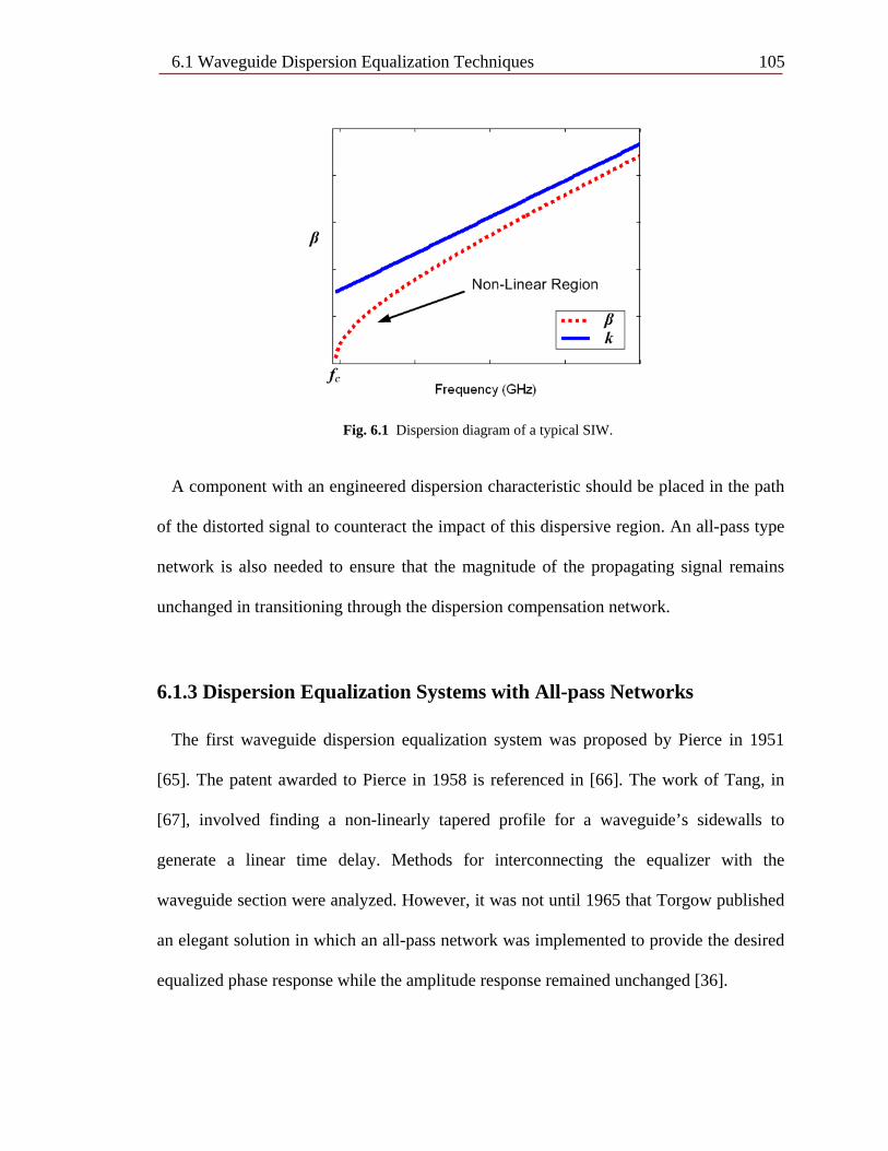
6.1 Waveguide Dispersion Equalization Techniques 105
Fig. 6.1 Dispersion diagram of a typical SIW.
A component with an engineered dispersion characteristic should be placed in the path
of the distorted signal to counteract the impact of this dispersive region. An all-pass type
network is also needed to ensure that the magnitude of the propagating signal remains
unchanged in transitioning through the dispersion compensation network.
6.1.3 Dispersion Equalization Systems with All-pass Networks
The first waveguide dispersion equalization system was proposed by Pierce in 1951
[65]. The patent awarded to Pierce in 1958 is referenced in [66]. The work of Tang, in
[67], involved finding a non-linearly tapered profile for a waveguide’s sidewalls to
generate a linear time delay. Methods for interconnecting the equalizer with the
waveguide section were analyzed. However, it was not until 1965 that Torgow published
an elegant solution in which an all-pass network was implemented to provide the desired
equalized phase response while the amplitude response remained unchanged [36].
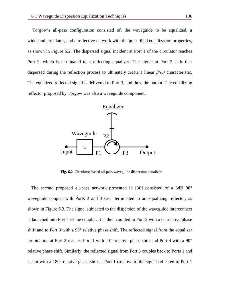
6.1 Waveguide Dispersion Equalization Techniques 106
Torgow’s all-pass configuration consisted of: the waveguide to be equalized, a
wideband circulator, and a reflective network with the prescribed equalization properties,
as shown in Figure 6.2. The dispersed signal incident at Port 1 of the circulator reaches
Port 2, which is terminated to a reflecting equalizer. The signal at Port 2 is further
dispersed during the reflection process to ultimately create a linear β(ω) characteristic.
The equalized reflected signal is delivered to Port 3, and thus, the output. The equalizing
reflector proposed by Torgow was also a waveguide component.
Waveguide
P1
P2
P3 Output
Equalizer
Input
Fig. 6.2 Circulator-based all-pass waveguide dispersion equalizer.
The second proposed all-pass network presented in [36] consisted of a 3dB 90°
waveguide coupler with Ports 2 and 3 each terminated to an equalizing reflector, as
shown in Figure 6.3. The signal subjected to the dispersion of the waveguide interconnect
is launched into Port 1 of the coupler. It is then coupled to Port 2 with a 0° relative phase
shift and to Port 3 with a 90° relative phase shift. The reflected signal from the equalizer
termination at Port 2 reaches Port 1 with a 0° relative phase shift and Port 4 with a 90°
relative phase shift. Similarly, the reflected signal from Port 3 couples back to Ports 1 and
4, but with a 180° relative phase shift at Port 1 (relative to the signal reflected to Port 1
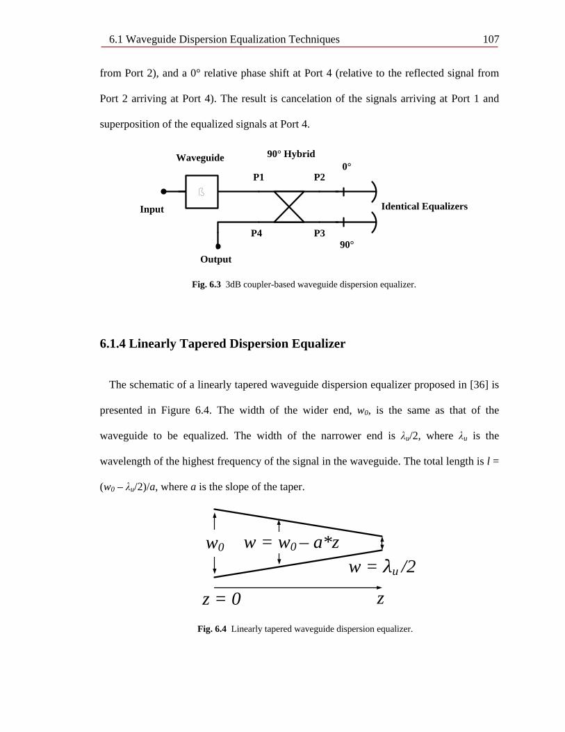
6.1 Waveguide Dispersion Equalization Techniques 107 from Port 2), and a 0° relative phase shift at Port 4 (relative to the reflected signal from
Port 2 arriving at Port 4). The result is cancelation of the signals arriving at Port 1 and
superposition of the equalized signals at Port 4.
90° HybridWaveguide
P1 P2
P3P4
Output
Input Identical Equalizers
0°
90°
Fig. 6.3 3dB coupler-based waveguide dispersion equalizer. 6.1.4 Linearly Tapered Dispersion Equalizer
The schematic of a linearly tapered waveguide dispersion equalizer proposed in [36] is
presented in Figure 6.4. The width of the wider end, w0, is the same as that of the
waveguide to be equalized. The width of the narrower end is λu/2, where λu is the
wavelength of the highest frequency of the signal in the waveguide. The total length is l =
(w0 – λu/2)/a, where a is the slope of the taper.
w0
z = 0 z
w = w0 – a*zw = λu /2
Fig. 6.4 Linearly tapered waveguide dispersion equalizer.
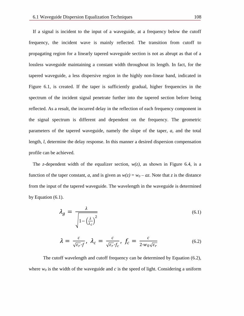
6.1 Waveguide Dispersion Equalization Techniques 108
If a signal is incident to the input of a waveguide, at a frequency below the cutoff
frequency, the incident wave is mainly reflected. The transition from cutoff to
propagating region for a linearly tapered waveguide section is not as abrupt as that of a
lossless waveguide maintaining a constant width throughout its length. In fact, for the
tapered waveguide, a less dispersive region in the highly non-linear band, indicated in
Figure 6.1, is created. If the taper is sufficiently gradual, higher frequencies in the
spectrum of the incident signal penetrate further into the tapered section before being
reflected. As a result, the incurred delay in the reflection of each frequency component in
the signal spectrum is different and dependent on the frequency. The geometric
parameters of the tapered waveguide, namely the slope of the taper, a, and the total
length, l, determine the delay response. In this manner a desired dispersion compensation
profile can be achieved.
The z-dependent width of the equalizer section, w(z), as shown in Figure 6.4, is a
function of the taper constant, a, and is given as w(z) = w0 – az. Note that z is the distance
from the input of the tapered waveguide. The wavelength in the waveguide is determined
by Equation (6.1).
𝜆𝜆𝑙𝑙 = 𝜆𝜆
�1− � 𝜆𝜆𝜆𝜆𝑐𝑐�
2 (6.1)
𝜆𝜆 = 𝑐𝑐
√𝜀𝜀𝑟𝑟 ∙𝑓𝑓, 𝜆𝜆𝑐𝑐 = 𝑐𝑐
√𝜀𝜀𝑟𝑟 ∙𝑓𝑓𝑐𝑐, 𝑓𝑓𝑐𝑐 = 𝑐𝑐
2∙𝑤𝑤0√𝜀𝜀𝑟𝑟 (6.2)
The cutoff wavelength and cutoff frequency can be determined by Equation (6.2),
where w0 is the width of the waveguide and c is the speed of light. Considering a uniform
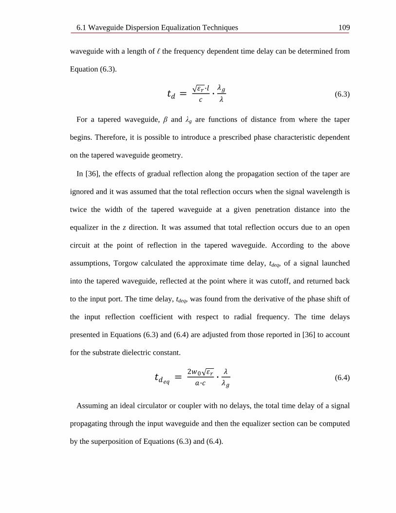
6.1 Waveguide Dispersion Equalization Techniques 109 waveguide with a length of ℓ the frequency dependent time delay can be determined from
Equation (6.3).
𝑡𝑡𝑑𝑑 = √𝜀𝜀𝑟𝑟 ∙𝑡𝑡𝑐𝑐
∙ 𝜆𝜆𝑙𝑙𝜆𝜆
(6.3)
For a tapered waveguide, β and λg are functions of distance from where the taper
begins. Therefore, it is possible to introduce a prescribed phase characteristic dependent
on the tapered waveguide geometry.
In [36], the effects of gradual reflection along the propagation section of the taper are
ignored and it was assumed that the total reflection occurs when the signal wavelength is
twice the width of the tapered waveguide at a given penetration distance into the
equalizer in the z direction. It was assumed that total reflection occurs due to an open
circuit at the point of reflection in the tapered waveguide. According to the above
assumptions, Torgow calculated the approximate time delay, tdeq, of a signal launched
into the tapered waveguide, reflected at the point where it was cutoff, and returned back
to the input port. The time delay, tdeq, was found from the derivative of the phase shift of
the input reflection coefficient with respect to radial frequency. The time delays
presented in Equations (6.3) and (6.4) are adjusted from those reported in [36] to account
for the substrate dielectric constant.
𝑡𝑡𝑑𝑑𝑒𝑒𝑒𝑒 = 2𝑤𝑤0√𝜀𝜀𝑟𝑟𝑎𝑎∙𝑐𝑐
∙ 𝜆𝜆𝜆𝜆𝑙𝑙
(6.4)
Assuming an ideal circulator or coupler with no delays, the total time delay of a signal
propagating through the input waveguide and then the equalizer section can be computed
by the superposition of Equations (6.3) and (6.4).
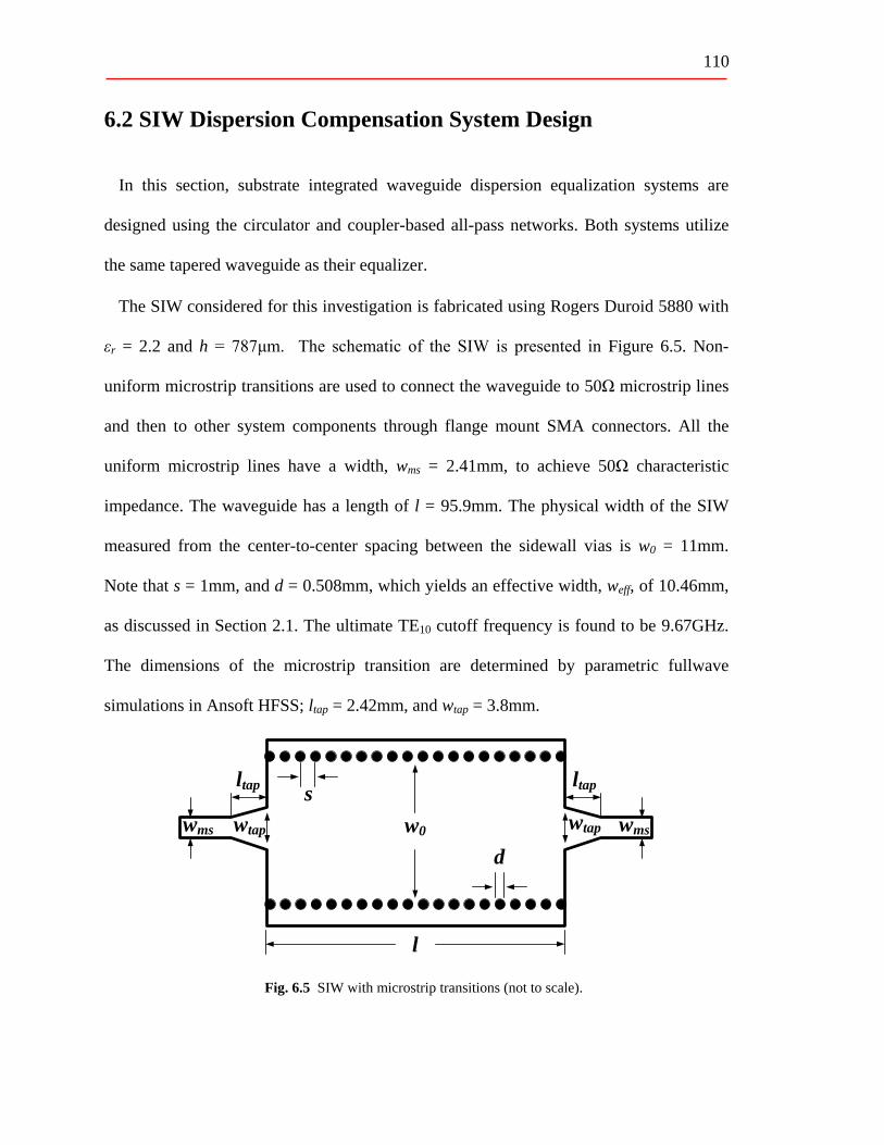
110
6.2 SIW Dispersion Compensation System Design
In this section, substrate integrated waveguide dispersion equalization systems are
designed using the circulator and coupler-based all-pass networks. Both systems utilize
the same tapered waveguide as their equalizer.
The SIW considered for this investigation is fabricated using Rogers Duroid 5880 with
εr = 2.2 and h = 787μm. The schematic of the SIW is presented in Figure 6.5. Non-
uniform microstrip transitions are used to connect the waveguide to 50Ω microstrip lines
and then to other system components through flange mount SMA connectors. All the
uniform microstrip lines have a width, wms = 2.41mm, to achieve 50Ω characteristic
impedance. The waveguide has a length of l = 95.9mm. The physical width of the SIW
measured from the center-to-center spacing between the sidewall vias is w0 = 11mm.
Note that s = 1mm, and d = 0.508mm, which yields an effective width, weff, of 10.46mm,
as discussed in Section 2.1. The ultimate TE10 cutoff frequency is found to be 9.67GHz.
The dimensions of the microstrip transition are determined by parametric fullwave
simulations in Ansoft HFSS; ltap = 2.42mm, and wtap = 3.8mm.
wms wtap
ltap
w0 wms
ltap
wtap
l
s
d
Fig. 6.5 SIW with microstrip transitions (not to scale).
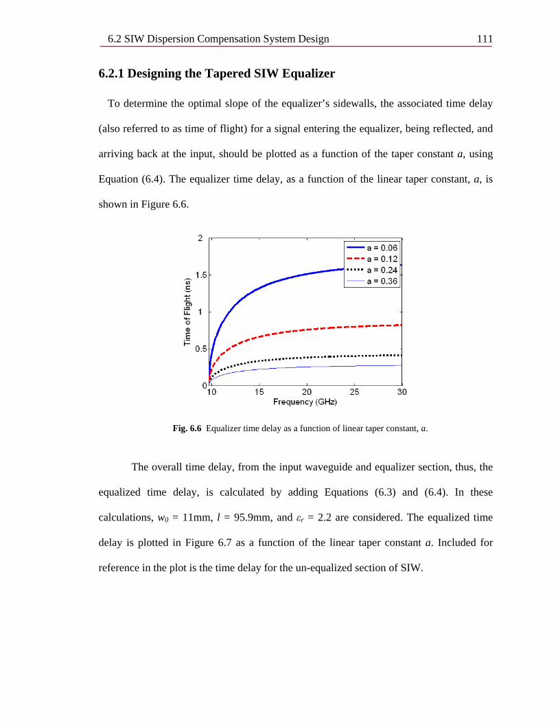
6.2 SIW Dispersion Compensation System Design 111 6.2.1 Designing the Tapered SIW Equalizer
To determine the optimal slope of the equalizer’s sidewalls, the associated time delay
(also referred to as time of flight) for a signal entering the equalizer, being reflected, and
arriving back at the input, should be plotted as a function of the taper constant a, using
Equation (6.4). The equalizer time delay, as a function of the linear taper constant, a, is
shown in Figure 6.6.
Fig. 6.6 Equalizer time delay as a function of linear taper constant, a.
The overall time delay, from the input waveguide and equalizer section, thus, the
equalized time delay, is calculated by adding Equations (6.3) and (6.4). In these
calculations, w0 = 11mm, l = 95.9mm, and εr = 2.2 are considered. The equalized time
delay is plotted in Figure 6.7 as a function of the linear taper constant a. Included for
reference in the plot is the time delay for the un-equalized section of SIW.
6.2 SIW Dispersion Compensation System Design 112
Fig. 6.7 Total equalized time delay as a function of linear taper constant, a.
The goal of dispersion equalization for waveguides operating near cutoff is to minimize
the time delay discrepancy between the lower and upper frequency bands. From Figure
6.7, it is determined that the linear taper constant a = 0.12, provides the best time delay
equalization. Assuming the equalizer taper extends from the input width of 11mm down
to zero width, a tapered equalizer with slope of a = 0.12 would require a length of
91.6mm, which is nearly equal to the entire length of the original SIW interconnect. In
order to keep the equalizer rather compact, a slope of a = 0.24 was considered sufficient.
In Figure 6.7, for the un-equalized SIW, the time delay is observed to be 1.866ns at
10GHz, 0.6203ns at 15GHz, and 0.5142ns at 25GHz. With the inclusion of the linearly
tapered delay equalizer, the time delay is observed to be 1.976ns at 10GHz, 0.9496ns at
15GHz, and 0.9114ns at 25GHz. There is an unavoidable dispersive effect directly at the
cutoff frequency. However, it is clear that the linearly tapered equalizer provides
significant improvement in equalizing the delay (or time of flight) for most of the band
except near cutoff.

6.2 SIW Dispersion Compensation System Design 113
If the time delay near the middle of the operating bandwidth is subtracted from the time
delay just above the cutoff region, an approximation of the maximum time delay
discrepancy in the highly dispersive region can be found. Similarly, by subtracting the
time delay at the upper frequency band from the time delay at a frequency in the middle
of the operating bandwidth, an approximation of the maximum time delay discrepancy in
the more linear operating band can be found. It can be seen that the designed equalizer
provides a 219ps decrease in the approximation of the maximum time delay discrepancy
between 10GHz and 15GHz. In considering the upper frequency band between 15GHz
and 25GHz, the time delay discrepancy is 38.2ps for the equalized SIW, compared to
106.1ps for the un-equalized waveguide. From the calculations in the higher frequency
band, it is clear that the equalizer provides nearly a threefold improvement in the time
delay discrepancy.
6.2.2 Characterizing the Designed Reflective Equalizer Component
In order to characterize the waveguide and equalizer sections, fullwave simulations are
conducted in Ansoft HFSS. To interface the tapered SIW equalizer to a 50Ω circulator or
coupler, a microstrip transition, as described earlier, is used. The equalizer geometry is
shown in Figure 6.8.
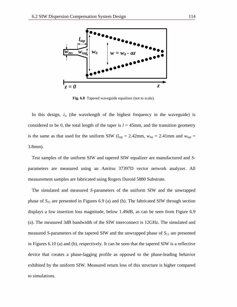
6.2 SIW Dispersion Compensation System Design 114
wms wtap
ltap
w0 w = w0 - az
zz = 0
Fig. 6.8 Tapered waveguide equalizer (not to scale).
In this design, λu (the wavelength of the highest frequency in the waveguide) is
considered to be 0, the total length of the taper is l = 45mm, and the transition geometry
is the same as that used for the uniform SIW (ltap = 2.42mm, wms = 2.41mm and wtap =
3.8mm).
Test samples of the uniform SIW and tapered SIW equalizer are manufactured and S-
parameters are measured using an Anritsu 37397D vector network analyzer. All
measurement samples are fabricated using Rogers Duroid 5880 Substrate.
The simulated and measured S-parameters of the uniform SIW and the unwrapped
phase of S21 are presented in Figures 6.9 (a) and (b). The fabricated SIW through section
displays a low insertion loss magnitude, below 1.49dB, as can be seen from Figure 6.9
(a). The measured 3dB bandwidth of the SIW interconnect is 12GHz. The simulated and
measured S-parameters of the tapered SIW and the unwrapped phase of S11 are presented
in Figures 6.10 (a) and (b), respectively. It can be seen that the tapered SIW is a reflective
device that creates a phase-lagging profile as opposed to the phase-leading behavior
exhibited by the uniform SIW. Measured return loss of this structure is higher compared
to simulations.
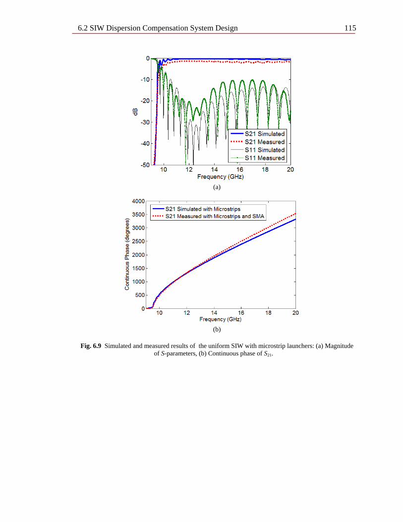
6.2 SIW Dispersion Compensation System Design 115
(a)
(b)
Fig. 6.9 Simulated and measured results of the uniform SIW with microstrip launchers: (a) Magnitude
of S-parameters, (b) Continuous phase of S21.
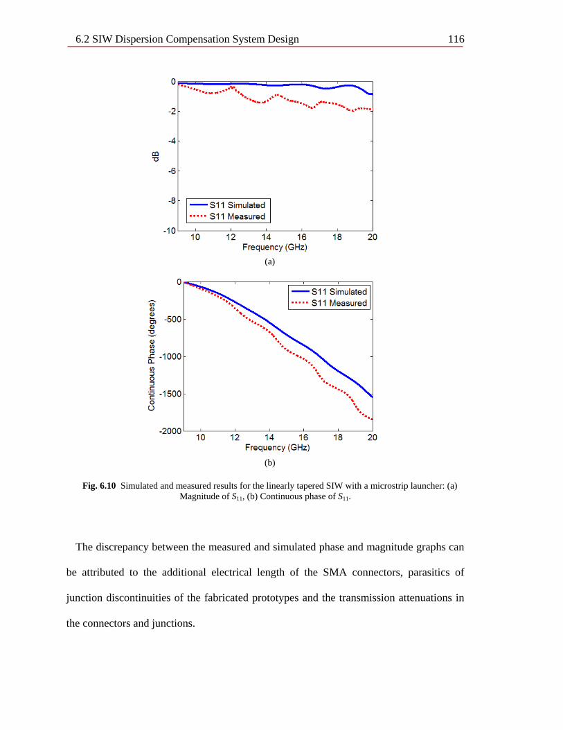
6.2 SIW Dispersion Compensation System Design 116
(a)
(b)
Fig. 6.10 Simulated and measured results for the linearly tapered SIW with a microstrip launcher: (a)
Magnitude of S11, (b) Continuous phase of S11.
The discrepancy between the measured and simulated phase and magnitude graphs can
be attributed to the additional electrical length of the SMA connectors, parasitics of
junction discontinuities of the fabricated prototypes and the transmission attenuations in
the connectors and junctions.
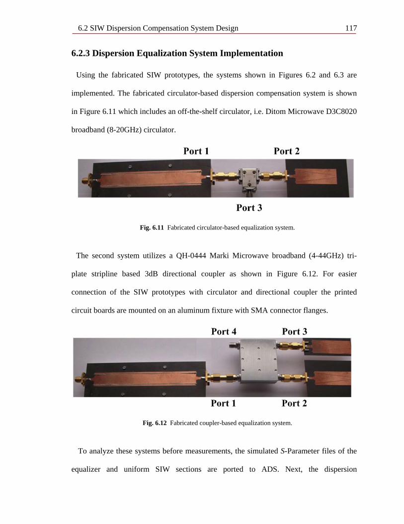
6.2 SIW Dispersion Compensation System Design 117 6.2.3 Dispersion Equalization System Implementation
Using the fabricated SIW prototypes, the systems shown in Figures 6.2 and 6.3 are
implemented. The fabricated circulator-based dispersion compensation system is shown
in Figure 6.11 which includes an off-the-shelf circulator, i.e. Ditom Microwave D3C8020
broadband (8-20GHz) circulator.
Fig. 6.11 Fabricated circulator-based equalization system.
The second system utilizes a QH-0444 Marki Microwave broadband (4-44GHz) tri-
plate stripline based 3dB directional coupler as shown in Figure 6.12. For easier
connection of the SIW prototypes with circulator and directional coupler the printed
circuit boards are mounted on an aluminum fixture with SMA connector flanges.
Fig. 6.12 Fabricated coupler-based equalization system.
To analyze these systems before measurements, the simulated S-Parameter files of the
equalizer and uniform SIW sections are ported to ADS. Next, the dispersion
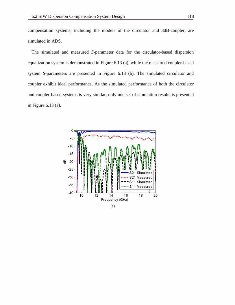
6.2 SIW Dispersion Compensation System Design 118 compensation systems, including the models of the circulator and 3dB-coupler, are
simulated in ADS.
The simulated and measured S-parameter data for the circulator-based dispersion
equalization system is demonstrated in Figure 6.13 (a), while the measured coupler-based
system S-parameters are presented in Figure 6.13 (b). The simulated circulator and
coupler exhibit ideal performance. As the simulated performance of both the circulator
and coupler-based systems is very similar, only one set of simulation results is presented
in Figure 6.13 (a).
(a)
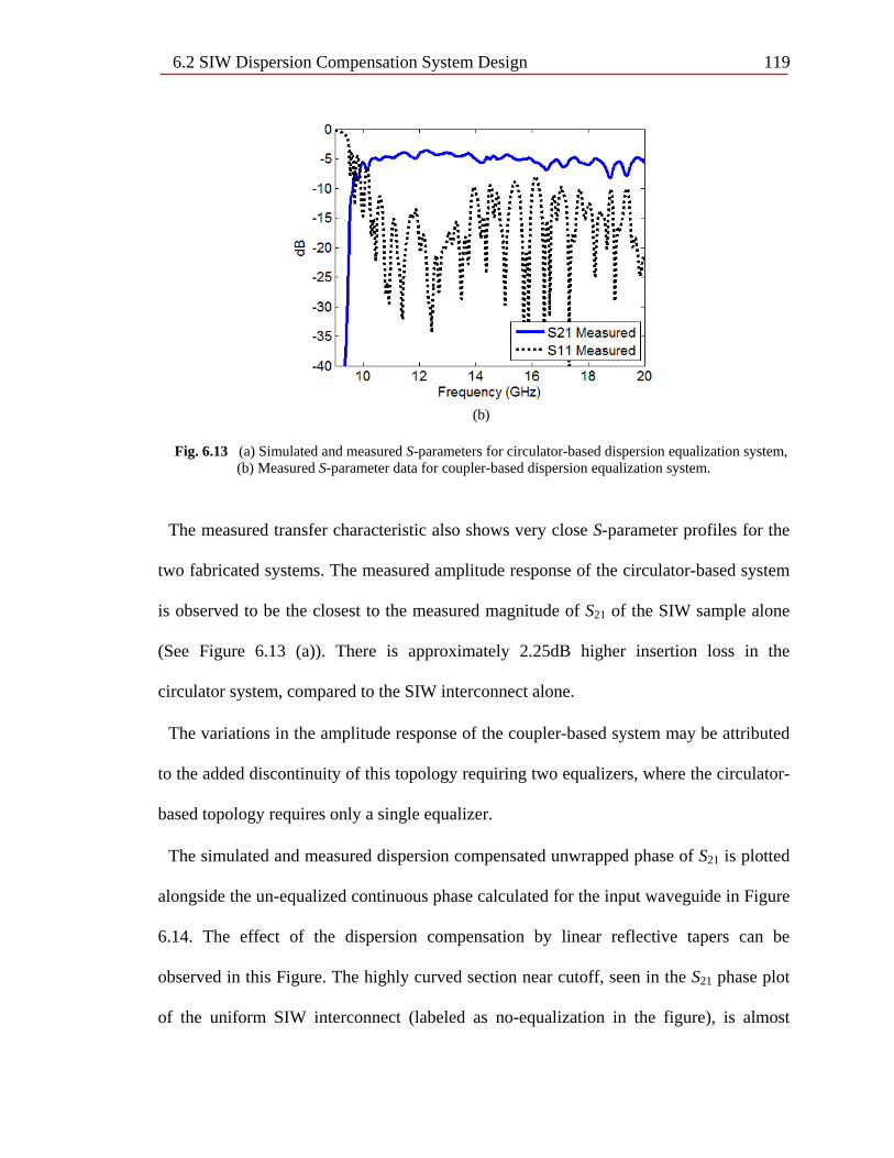
6.2 SIW Dispersion Compensation System Design 119
(b)
Fig. 6.13 (a) Simulated and measured S-parameters for circulator-based dispersion equalization system,
(b) Measured S-parameter data for coupler-based dispersion equalization system.
The measured transfer characteristic also shows very close S-parameter profiles for the
two fabricated systems. The measured amplitude response of the circulator-based system
is observed to be the closest to the measured magnitude of S21 of the SIW sample alone
(See Figure 6.13 (a)). There is approximately 2.25dB higher insertion loss in the
circulator system, compared to the SIW interconnect alone.
The variations in the amplitude response of the coupler-based system may be attributed
to the added discontinuity of this topology requiring two equalizers, where the circulator-
based topology requires only a single equalizer.
The simulated and measured dispersion compensated unwrapped phase of S21 is plotted
alongside the un-equalized continuous phase calculated for the input waveguide in Figure
6.14. The effect of the dispersion compensation by linear reflective tapers can be
observed in this Figure. The highly curved section near cutoff, seen in the S21 phase plot
of the uniform SIW interconnect (labeled as no-equalization in the figure), is almost
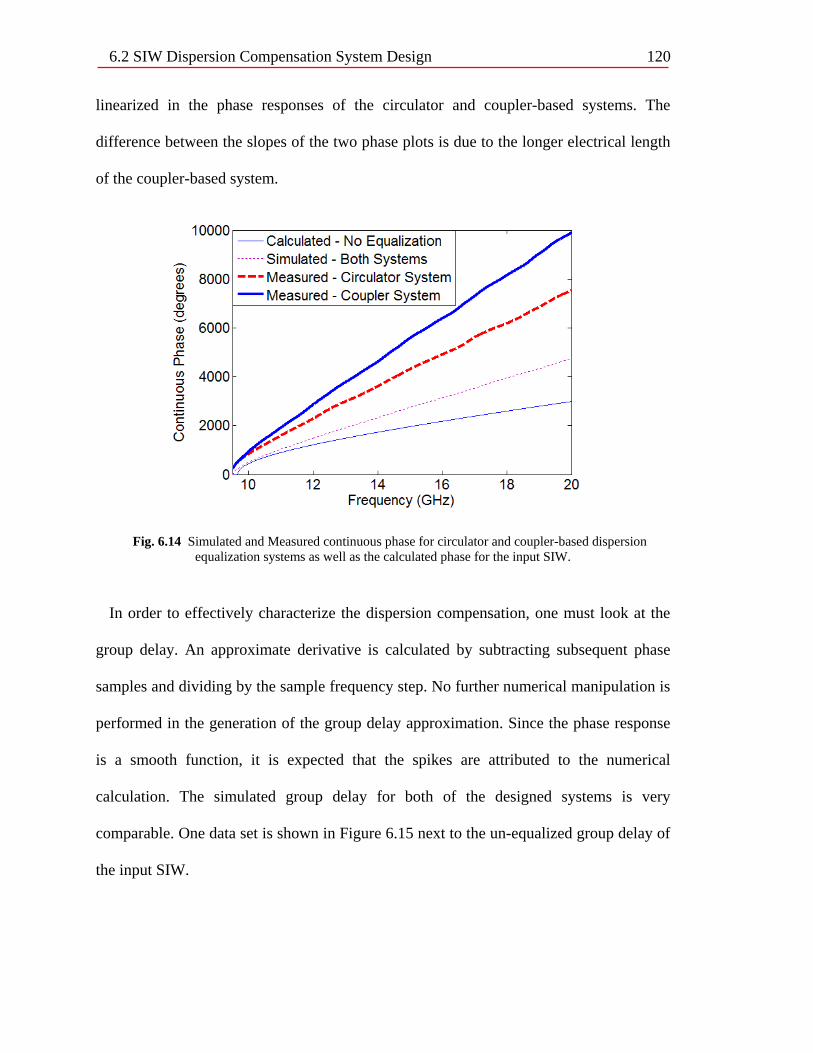
6.2 SIW Dispersion Compensation System Design 120 linearized in the phase responses of the circulator and coupler-based systems. The
difference between the slopes of the two phase plots is due to the longer electrical length
of the coupler-based system.
Fig. 6.14 Simulated and Measured continuous phase for circulator and coupler-based dispersion equalization systems as well as the calculated phase for the input SIW.
In order to effectively characterize the dispersion compensation, one must look at the
group delay. An approximate derivative is calculated by subtracting subsequent phase
samples and dividing by the sample frequency step. No further numerical manipulation is
performed in the generation of the group delay approximation. Since the phase response
is a smooth function, it is expected that the spikes are attributed to the numerical
calculation. The simulated group delay for both of the designed systems is very
comparable. One data set is shown in Figure 6.15 next to the un-equalized group delay of
the input SIW.
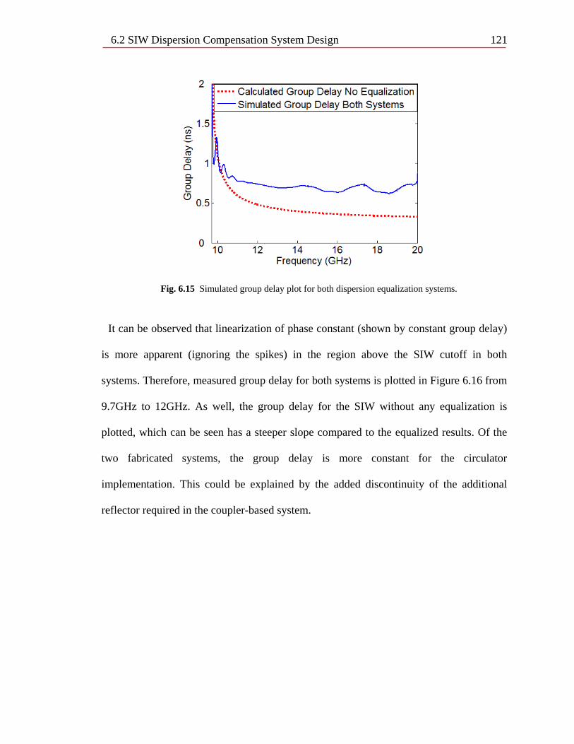
6.2 SIW Dispersion Compensation System Design 121
Fig. 6.15 Simulated group delay plot for both dispersion equalization systems.
It can be observed that linearization of phase constant (shown by constant group delay)
is more apparent (ignoring the spikes) in the region above the SIW cutoff in both
systems. Therefore, measured group delay for both systems is plotted in Figure 6.16 from
9.7GHz to 12GHz. As well, the group delay for the SIW without any equalization is
plotted, which can be seen has a steeper slope compared to the equalized results. Of the
two fabricated systems, the group delay is more constant for the circulator
implementation. This could be explained by the added discontinuity of the additional
reflector required in the coupler-based system.
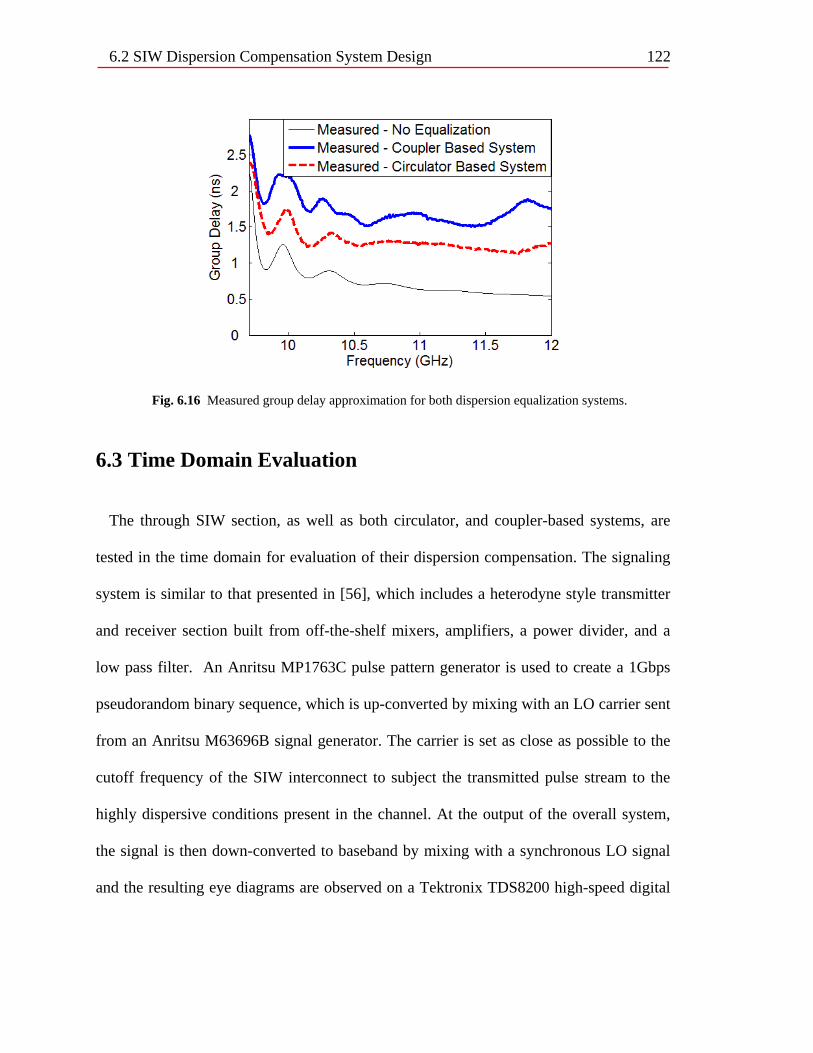
6.2 SIW Dispersion Compensation System Design 122
Fig. 6.16 Measured group delay approximation for both dispersion equalization systems.
6.3 Time Domain Evaluation
The through SIW section, as well as both circulator, and coupler-based systems, are
tested in the time domain for evaluation of their dispersion compensation. The signaling
system is similar to that presented in [56], which includes a heterodyne style transmitter
and receiver section built from off-the-shelf mixers, amplifiers, a power divider, and a
low pass filter. An Anritsu MP1763C pulse pattern generator is used to create a 1Gbps
pseudorandom binary sequence, which is up-converted by mixing with an LO carrier sent
from an Anritsu M63696B signal generator. The carrier is set as close as possible to the
cutoff frequency of the SIW interconnect to subject the transmitted pulse stream to the
highly dispersive conditions present in the channel. At the output of the overall system,
the signal is then down-converted to baseband by mixing with a synchronous LO signal
and the resulting eye diagrams are observed on a Tektronix TDS8200 high-speed digital
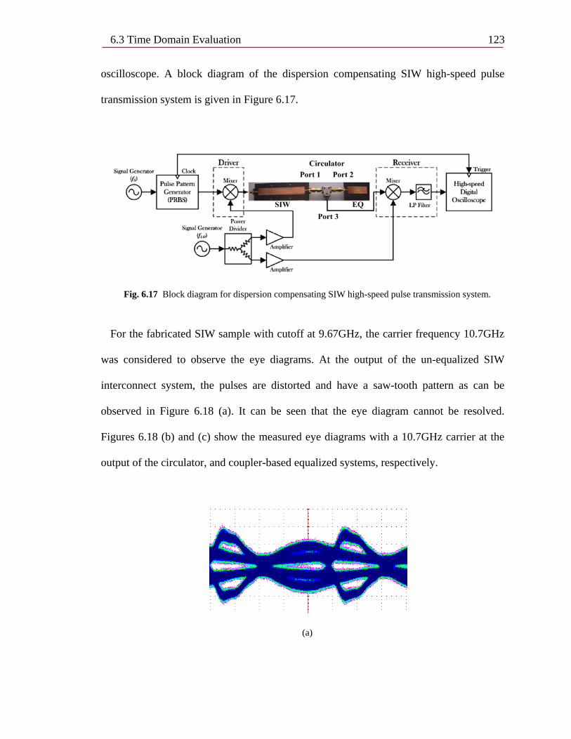
6.3 Time Domain Evaluation 123 oscilloscope. A block diagram of the dispersion compensating SIW high-speed pulse
transmission system is given in Figure 6.17.
Fig. 6.17 Block diagram for dispersion compensating SIW high-speed pulse transmission system.
For the fabricated SIW sample with cutoff at 9.67GHz, the carrier frequency 10.7GHz
was considered to observe the eye diagrams. At the output of the un-equalized SIW
interconnect system, the pulses are distorted and have a saw-tooth pattern as can be
observed in Figure 6.18 (a). It can be seen that the eye diagram cannot be resolved.
Figures 6.18 (b) and (c) show the measured eye diagrams with a 10.7GHz carrier at the
output of the circulator, and coupler-based equalized systems, respectively.
(a)
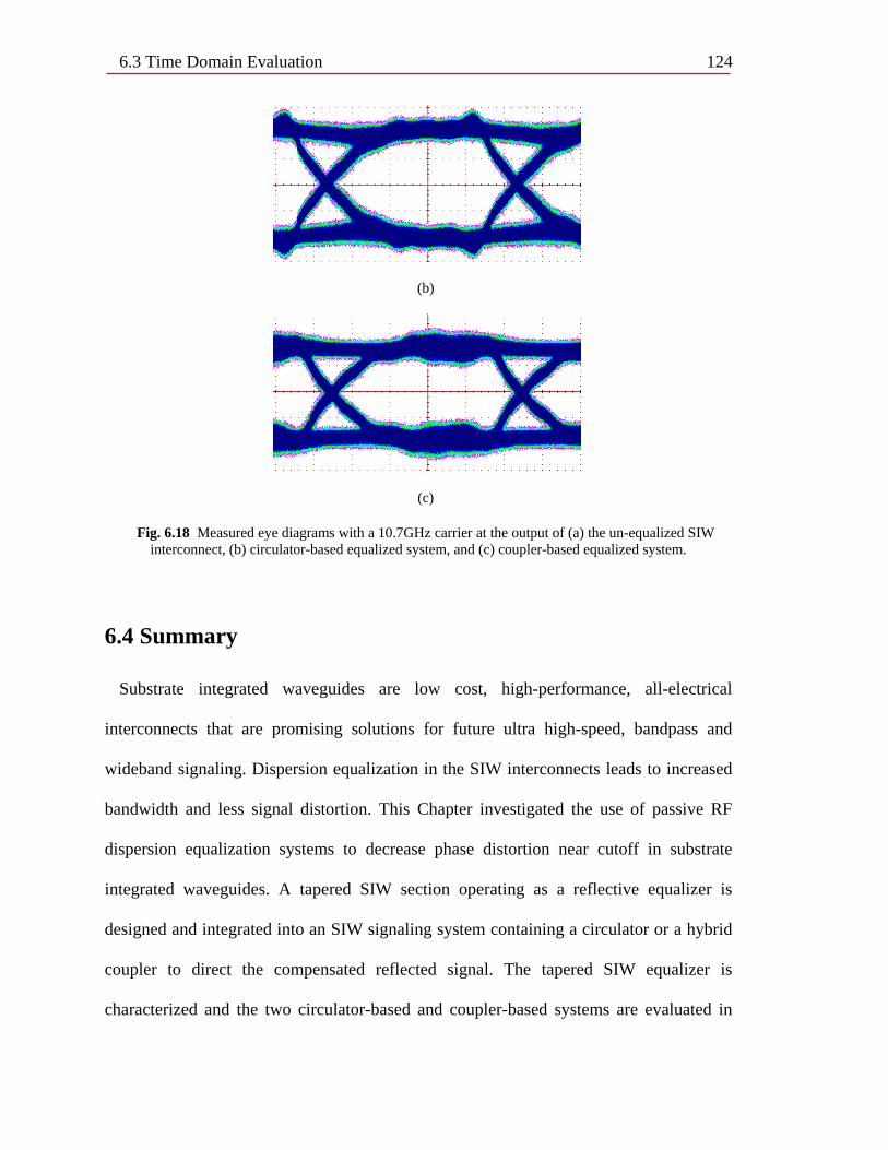
6.3 Time Domain Evaluation 124
(b)
(c)
Fig. 6.18 Measured eye diagrams with a 10.7GHz carrier at the output of (a) the un-equalized SIW interconnect, (b) circulator-based equalized system, and (c) coupler-based equalized system.
6.4 Summary
Substrate integrated waveguides are low cost, high-performance, all-electrical
interconnects that are promising solutions for future ultra high-speed, bandpass and
wideband signaling. Dispersion equalization in the SIW interconnects leads to increased
bandwidth and less signal distortion. This Chapter investigated the use of passive RF
dispersion equalization systems to decrease phase distortion near cutoff in substrate
integrated waveguides. A tapered SIW section operating as a reflective equalizer is
designed and integrated into an SIW signaling system containing a circulator or a hybrid
coupler to direct the compensated reflected signal. The tapered SIW equalizer is
characterized and the two circulator-based and coupler-based systems are evaluated in

6.3 Time Domain Evaluation 125 time and frequency domains. The efficacy of the proposed dispersion compensation
systems is demonstrated for the first time by measuring and comparing the output eye
diagrams with the output of an SIW interconnect when a 1 Gbps bit sequence is
transmitted near the cutoff region. Considerable eye opening is achieved in both systems
while the circulator-based system exhibits a better performance due to the lower number
of junctions and discontinuities.
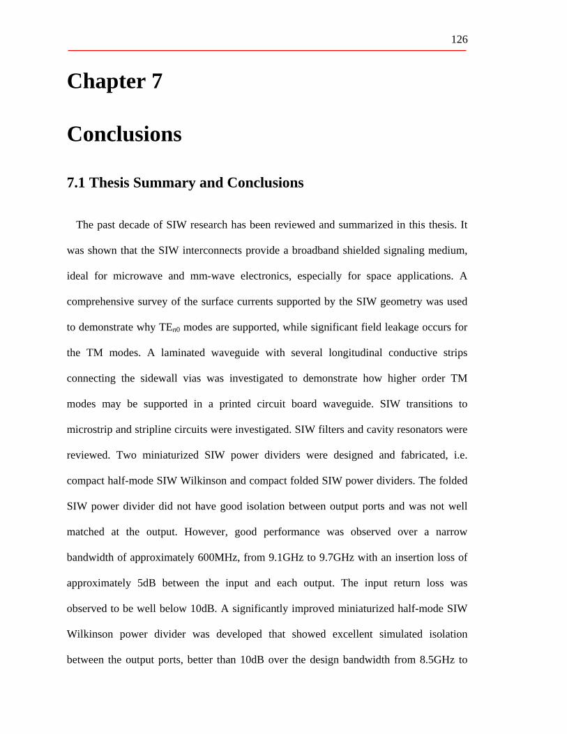
126
Chapter 7 Conclusions 7.1 Thesis Summary and Conclusions
The past decade of SIW research has been reviewed and summarized in this thesis. It
was shown that the SIW interconnects provide a broadband shielded signaling medium,
ideal for microwave and mm-wave electronics, especially for space applications. A
comprehensive survey of the surface currents supported by the SIW geometry was used
to demonstrate why TEn0 modes are supported, while significant field leakage occurs for
the TM modes. A laminated waveguide with several longitudinal conductive strips
connecting the sidewall vias was investigated to demonstrate how higher order TM
modes may be supported in a printed circuit board waveguide. SIW transitions to
microstrip and stripline circuits were investigated. SIW filters and cavity resonators were
reviewed. Two miniaturized SIW power dividers were designed and fabricated, i.e.
compact half-mode SIW Wilkinson and compact folded SIW power dividers. The folded
SIW power divider did not have good isolation between output ports and was not well
matched at the output. However, good performance was observed over a narrow
bandwidth of approximately 600MHz, from 9.1GHz to 9.7GHz with an insertion loss of
approximately 5dB between the input and each output. The input return loss was
observed to be well below 10dB. A significantly improved miniaturized half-mode SIW
Wilkinson power divider was developed that showed excellent simulated isolation
between the output ports, better than 10dB over the design bandwidth from 8.5GHz to

7.1 Thesis Summary and Conclusions 127 16GHz, with a maximum isolation of 42dB at 10.2GHz. Equal 3.9dB insertion loss in
power transmission to ports 2 and 3 was observed from simulations, while return loss at
all three ports was better than 10dB over the entire design bandwidth. In the fabricated
prototype, the 10dB return loss bandwidth was observed from 8.4GHz to 12.6GHz. The
discrepancy between simulation and measurement data can be attributed to the
discontinuities at the connector junction. The measured isolation for the half-mode power
divider was better than 10dB over the entire operating bandwidth with a maximum
isolation of over 40dB at 12.4GHz. The isolation provided by the new power divider is
considered a significant improvement over the previous “Y” branch rectangular SIW.
A low-cost, fully integrated SIW-based cavity resonator was designed and fabricated.
The RLC equivalent resonant circuit model was found by calculating the resonator
equivalent inductance and capacitance from the input impedance magnitude half-power
fractional bandwidth, as found from fullwave simulation data. Such a resonator may be
mass-produced with very low per-unit cost with tight manufacturing tolerances. It was
shown that the high quality factor of an SIW-based resonator provides excellent
frequency selectivity, even in a series coupled configuration. The SIW cavity resonator
was measured in an anechoic chamber to demonstrate its usefulness for antenna
applications. A series feedback microwave oscillator was designed using the new
resonator. The simulated output power was observed to be greater than 10dBm at 16GHz
with the second harmonic at 32GHz with a power of less than -60dBm. While the
fabricated oscillator had an error in the radial stub design, a phase noise of -82dBc/Hz
was measured at the free-running oscillation frequency of approximately 11GHz. A new
layout for the radial stub RF chokes was designed and harmonic balance simulations

7.1 Thesis Summary and Conclusions 128 were run to predict a free-running oscillation frequency at 16.12GHz with an output
power of 10dBm.
Dispersion equalization techniques were developed for the SIW interconnects.
Reflective SIW equalizer components were designed and fabricated. A 95.9mm long
SIW was fabricated and measurement results showed very low insertion loss on the order
of 1.5dB including SMA connectors and microstrip to SIW transitions. Two equalization
systems were presented with frequency and time domain experimental evaluations. The
circulator and coupler-based equalization systems each showed significantly more linear
continuous phase compared to the SIW with no equalization. Eye diagram measurements
for a 1Gbps signal were provided to show how the two equalization systems improve the
dispersion distortion near the SIW cutoff frequency.
7.2 Future Work Recommendations
Further analysis and design work is required for the folded SIW power divider and its
stripline transition. The design presented herein was only matched at the input port which
limits the applications suitable for the power divider. By improving the SMA to stripline
transitions, better measurement results should be possible for the current design.
The new layout for the series reflection oscillator presented in Chapter 5 must be
fabricated and tested in order to record accurate phase noise measurements at the actual
design frequency.
Further investigation into design of the reflective equalizing element and
miniaturization of SIW dispersion equalization systems is required, as the systems
presented in Chapter 6 are considerably bulky, especially for space applications. The

7.2 Future Work Recommendations 129 operation bandwidth of the tapered SIW should be improved. By effectively equalizing
the dispersion in the SIW interconnects, extremely wideband, distortion-less microwave,
and millimeter-wave links will be realized.
130
References [1] J. Hirokawa, M. Ando, “Single-Layer Feed Waveguide Consisting of Posts for
Plane TEM Wave Excitation in Parallel Plates,” IEEE Trans. Antennas Propagat., vol. 46, no. 5, May 1998.
[2] H. Uchimura, T. Takenoshita, M. Fujii, “Development of a Laminated
Waveguide,” IEEE Trans. Microw. Theory Tech., vol. 46, no. 12, December 1998.
[3] A. Suntives, R. Abhari, “Design and Characterization of the EBG Waveguide-Based Interconnects,” IEEE Trans. Adv. Packag., vol. 30, no. 2, May 2007.
[4] A. Patrovsky, M. Daigle, K. Wu, “Millimeter-wave Wideband Transition from CPW to Substrate Integrated Waveguide on Electrically Thick High-Permittivity Substrates,” Microwave Conference, 2007. European, pp. 138-141, 9-12, October 2007.
[5] D. Deslandes, K. Wu, “Integrated Microstrip and Rectangular Waveguide in
Planar Form,” IEEE Microw. Wireless Compon. Lett., vol. 11, no. 2, pp. 68-70, Feb. 2001.
[6] J. E. Rayas-Sánchez, “An Improved EM-Based Design Procedure for Single-
Layer Substrate Integrated Waveguide Interconnects with Microstrip Transitions,” Signal Integrity and High-Speed Interconnects, 2009. IMWS. IEEE MTT-S International Microwave Workshop Series on, pp. 27-30, 19-20, Feb. 2009.
[7] N. Grigoropoulos, B. Sanz-Izquierdo, P. R. Young, “Substrate Integrated Folded Waveguides (SIFW) and Filters,” IEEE Microw. Wireless Compon. Lett., vol. 15, no. 12, Dec. 2005.
[8] X. P. Chen, K. Wu, “Low-Loss Ultra-Wideband Transition between Conductor-
Backed Coplanar Waveguide and Substrate Integrated Waveguide,” Microwave Symposium Digest, 2009. MTT ’09. IEEE MTT-S International, pp. 349-352, 7-12, June 2009.
[9] S. Lee, S. Jung, H. Y. Lee, “Ultra-Wideband CPW-to-Substrate Integrated
Waveguide Transition Using an Elevated-CPW Section,” IEEE Microw. Wireless Compon. Lett., vol. 18, no. 11, pp. 746-748, Nov. 2008.
[10] T. J. Coenen, D. J. Bekers, J. L. Tauritz, F. E. Van Vliet, “Design and
Measurement of Metallic Post-Wall Waveguide Components,” Microwave Symposium Digest, 2009. MTT ’09. IEEE MTT-S International, pp. 261-264, 7-12, June 2009.
References 131
[11] B. Sanz-Izquierdo, N. Grigoropoulos, P. R. Young, “Ultra-Wideband Multilayer Substrate Integrated Folded Waveguides,” Microwave Symposium Digest, 2006. MTT ’09. IEEE MTT-S International, pp. 610-612, 11-16, June 2006.
[12] W. Hong, B. Liu, Y. Wang, Q. Lai, H. Tang, X. X. Yin, Y. D. Dong, Y. Zhang, K. Wu, “Half Mode Substrate Integrated Waveguide: A New Guided Wave Structure for Microwave and Millimeter Wave Application,” Infrared Millimeter Waves and 14th International Conference on Teraherz Electronics, 2006. IRMMW-THz 2006. Joint 31st International Conference on, pp. 219, 18-22 September 2006.
[13] W. Che, L. Geng, K. Deng, Y. L. Chow, “Analysis and Experiments of Compact Folded Substrate-Integrated Waveguide,” IEEE Trans. Microw. Theory Tech., vol. 56, no. 1, Jan. 2008.
[14] M. Bozzi, S. A. Winkler, K. Wu, “Novel Compact and Broadband Interconnects
Based on Ridge Substrate Integrated Waveguide,” Microwave Symposium Digest, 2009. MTT ’09. IEEE MTT-S International, pp. 121-124, 7-12, June 2009.
[15] G. H. Zhai, W. Hong, K. Wu, J. X. Chen, P. Chen, J. Wei, H. J. Tang, “Folded
Half Mode Substrate Integrated Waveguide 3 dB Coupler,” IEEE Microw. Wireless Compon. Lett., vol. 18, no. 8, Aug. 2008.
[16] B. Liu, W. Hong, Y.-Q. Wang, Q.-H. Lai, K. Wu, “Half Mode Substrate Integrated (HMSIW) 3-dB Coupler,” IEEE Microw. Wireless Compon. Lett., vol. 17, no. 1, January 2007.
[17] B. Liu, W. Hong, Y. Zhang, H. J. Tang, X. Yin, K. Wu, “Half Mode Substrate Integrated Waveguide 180° 3-dB Directional Couplers,” IEEE Trans. Microw. Theory Tech., vol. 55, no. 12, pp. 2586-2592, Dec. 2007.
[18] G. H. Zhai, W. Hong, K. Wu, J. X. Chen, P. Chen, H. J. Tang, “Substrate Integrated Folded Waveguide (SIFW) Narrow-wall Directional Coupler,” Microwave and Millimeter Wave Technology, 2008. ICMMT 2008, International Conference on, vol. 1, pp. 174-177, 21-24, April 2008.
[19] Y. Ding, K. Wu, “Miniaturized Hybrid Ring Circuits Using T-Type Folded Substrate Integrated Waveguide (TFSIW),” Microwave Symposium Digest, 2009. MTT ’09. IEEE MTT-S International, pp. 705-708, 7-12, June 2009.
[20] T. M. Shen, T. Y. Huang, R. B. Wu, “A Laminated Waveguide Magic-T in Multilayer LTCC,” Microwave Symposium Digest, 2009. MTT ’09. IEEE MTT-S International, pp. 713-716, 7-12, June 2009.
[21] H. J. Tang, W. Hong, J. X. Chen, G. Q. Luo, K. Wu, “Development of
Millimeter-Wave Planar Diplexers Based on Complimentary Characters of Dual-
References 132
Mode Substrate Integrated Waveguide Filters with Circular and Elliptic Cavities,” IEEE Trans. Microw. Theory Tech., vol. 55, no. 4, pp. 776-782 Apr. 2007.
[22] Z. Hao, W. Hong, H. Li, H. Zhang, K. Wu, “Multiway Broadband Substrate
Integrated Waveguide (SIW) Power Divider,” Antennas and Propagation Society International Symposium, 2005 IEEE, vol. 1A, pp. 639-642, 3-8, July 2005.
[23] Z. Y. Zhang, K. Wu, “Broadband Half-Mode Substrate Integrated Waveguide
(HMSIW) Wilkinson Power Divider,” Microwave Symposium Digest, 2008 IEEE MTT-S International, pp. 879-882, 15-20, June 2008.
[24] M. J. Hill, R. W. Ziolkowski, J. Papapolymerou, “A High-Q Reconfigurable
Planar EBG Cavity Resonator,” IEEE Microw. Wireless Compon. Lett., vol. 11, no. 6, Dec. 2001.
[25] Y. Cassivi, L. Perregrini, K. Wu, G. Conciauro, “Low-Cost and High-Q
Millimeter-Wave Resonator Using Substrate Integrated Waveguide Technique,” European Microwave Conference, 2002. 32nd, pp. 1-4, Oct. 2002.
[26] I. Ocket, A. Phommahaxay, H. A. C. Tilmans, J. B. Mills, B. Nauwelaers,
“Millimeter Wave Micromachined Cavity Resonators on MCM-D: Oscillator-Resonator Co-Design and Packaging Considerations,” Microwave Symposium Digest, 2009. MTT ’09. IEEE MTT-S International, pp. 593-596, 7-12, June 2009.
[27] Z. C. Hao, W. Hong, X. P. Chen, J. X. Chen, K. Wu, “A Single-Layer Folded
Substrate Integrated Waveguide (SIW) Filter,” Microwave Conference Proceedings, 2005. APMC. Asia-Pacific Conference Proceedings, vol. 1, pp. 3-4, 4-7, Dec. 2005.
[28] X. P. Chen, K. Wu, Z. L. Li, “Dual-Band and Triple-Band Substrate Integrated
Waveguide Filters with Chebyshev and Quasi-Elliptic Responses,” IEEE Trans. Microw. Theory Tech., vol. 55, no. 12, pp. 2569-2578 Dec. 2007.
[29] O. Glubokov, D. Budimir, “Substrate Integrated Folded-Waveguide Cross-Coupled Filter with Negative Coupling Structure,” Antennas and Propagation Society International Symposium, 2009. APSURSI ’09. IEEE, 1-5, June 2009.
[30] X. P. Chen, K. Wu, D. Drolet, “Substrate Integrated Waveguide Filter with Improved Stopband Performance for Satellite Ground Terminal,” IEEE Trans. Microw. Theory Tech., vol. 57, no. 3, pp. 674-683 Mar. 2009.
[31] K. K. Samanta, D. Stephens, I. D. Robertson, “Design and Performance of a
60GHz Multi-Chip Module Receiver Employing Substrate Integrated Waveguides,” Microwaves, Antennas, & Propagation, IET, vol. 1, no. 5, pp. 961-967, Oct. 2007.
References 133
[32] D. Kim, J. W. Lee, C. S. Cho, T. K. Lee, “X-Band Circular Ring-Slot Antenna
Embedded in Single-Layer SIW for Circular Polarization,” Electronics Letters, vol. 45, no. 13, pp. 668-669, June 18 2009.
[33] D. Kim, T. Seo, J. Lee, C. S. Cho, “Design of Circular Polarized Antenna using
SIW Feeding and Cavity,” IEEE 2009 (Future Publication). [34] M. Daneshmand, R. R. Mansour, "Multiport MEMS-based Waveguide and
Coaxial Switches," Microwave Theory and Techniques, IEEE Transactions on , vol.53, no.11, pp. 3531-3537, Nov. 2005.
[35] Y. Cassivi, K. Wu, “Low Cost Microwave Oscillator Using Substrate Integrated
Waveguide Cavity,” IEEE Microw. Wireless Compon. Lett., vol. 13, no. 2, pp. 48-50, Feb. 2003.
[36] E. N. Torgow, “Equalization of Waveguide Delay Distortion,” IEEE Trans.
Microw. Theory Tech., vol. MTT-13, no. 6, Nov. 1965. [37] H. Li, W. Hong, T. J. Cui, K. Wu, Y. L. Zhang, L. Yan, “Propagation
Characteristics of Substrate Integrated Waveguide Based on LTCC,” IEEE MTT-S Digest, pp. 2045-2048, 2003.
[38] F. Xu, K. Wu, “Guided-Wave and Leakage Characteristics of Substrate Integrated
Waveguide,” IEEE Trans. Microw. Theory Tech., vol. 53, no. 1, January 2005. [39] D. Stephens, P. R. Young, I.D. Robertson, “Millimeter-Wave Substrate Integrated
Waveguides and Filters in Photoimageable Thick-film Technology,” IEEE Trans. Microw. Theory Tech., vol. 53, no. 12, December 2005.
[40] L. J. Lavedan, “Design of Waveguide-to-Microstrip Transitions Specially Suited to Millimeter-Wave Applications,” Electronics Letters, vol. 13, no. 20, pp. 604-605, Sept. 1977.
[41] R. Bai, Y. L. Dong, J. Xu, “Broadband Waveguide-to-Microstrip Antipodal Finline Transition without Additional Resonance Preventer,” Microwave, Antenna, Propagation and EMC Technologies for Wireless Communications, 2007 International Symposium on, pp. 385-388, 16-17, Aug. 2007.
[42] J. D. Gibson et al., The Communications Handbook, 2nd Ed. CRC Press, section 68-10-12, 2002
[43] Z. Li, K. Wu, “24-GHz Frequency-Modulation Continuous-Wave Radar Front-
End System-on-Substrate,” IEEE Trans. Microw. Theory Tech., vol. 56, no. 2, Feb. 2008.
References 134
[44] D. M. Pozar, “Microwave Engineering,” 3rd Ed. John Wiley & Sons, 2005.
[45] Y. Cassivi, L. Perregrini, P. Arcioni, M. Bressan, K. Wu, G. Conciauro,
“Dispersion Characteristics of Substrate Integrated Rectangular Waveguide,” IEEE Microw. Wireless Compon. Lett., vol. 12, no. 9, Sept. 2002.
[46] High Frequency Structure Simulator (HFSS) ver. 10.1, Ansoft Corporation, Pittsburgh, PA, 2006.
[47] G. G. Mazumder, P. K. Saha, “A Novel Rectangular Waveguide with Double T-Septums (Short Paper),” IEEE Trans. Microw. Theory Tech., vol. 33, no. 11, Nov. 1985.
[48] S. Germain, D. Deslandes, K. Wu, “Development of Substrate Integrated
Waveguide Power Dividers,” Electrical and Computer Engineering, 2003. IEEE CCECE 2003. Canadian Conference on, vol. 3, pp. 1921-1924, 4-7, May 2003.
[49] J.-X. Chen, W. Hong, Z.-C. Hao, H.-J. Tang, K. Wu, “High isolation sub-harmonic up-converter using substrate integrated waveguide,” IEEE Electronics Letters, vol. 41, no. 22, Oct. 2005.
[50] F. Mira, J. Mateu, S. Cogollos, V. E. Boria, “Design of Ultra-Wideband Substrate
Integrated Waveguide (SIW) Filters in Zigzag Topology,” IEEE Microw. Wireless Compon. Lett., vol. 19, no. 5, pp. 281-283, May 2009.
[51] Y. Wang, W. Hong, Y. Dong, B. Liu, H. J. Tang, J. Chen, X. Yin, K. Wu, “Half Mode Substrate Integrated Waveguide (HMSIW) Bandpass Filter,” IEEE Microw. Wireless Compon. Lett., vol. 17, no. 4, April 2007.
[52] L. S. Wu, X. L. Zhou, W. Y. Yin, “Evanescent-Mode Bandpass Filters Using Folded and Ridge Substrate Integrated Waveguides (SIWs),” IEEE Microw. Wireless Compon. Lett., vol. 19, no. 3, pp. 161-163, Mar. 2009.
[53] J. X. Chen, W. Hong, Z. C. Hao, H. Li, K. Wu, “Development of a Low Cost Microwave Mixer Using a Broad-band Substrate Integrated Waveguide (SIW) Coupler,” IEEE Microw. Wireless Compon. Lett., vol. 16, no. 2, pp. 84-86, Feb. 2006.
[54] J. X. Chen, W. Hong, H. J. Tang, X. X. Yin, K. Wu, “A Compact Millimeter-
Wave Mixer Module,” Microwave Conference Proceedings, 2005. APMC 2005. Asia-Pacific Conference Proceedings, vol. 5, pp. 3-5, 4-7, Dec. 2005.
References 135
[55] A. Suntives, R. Abhari, “Ultra-High-Speed Multichannel Data Transmission Using Hybrid Substrate Integrated Waveguides,” IEEE Trans. Microw. Theory Tech., vol. 56, no. 8, pp. 1973-1984 Aug. 2008.
[56] A. Suntives, R. Abhari, “Design and Application of Multimode Substrate Integrated Waveguides in Parallel Multichannel Signaling Systems,” IEEE Trans. Microw. Theory Tech., vol. 57, no. 6, pp. 1563-1571 June 2009.
[57] E. J. Wilkinson, “An N-Way Hybrid Power Divider,” Microwave Theory and
Techniques, IRE Transactions on, vol. 8, no. 1, pp. 116-118, Jan. 1960. [58] H. H. Jhuang, T. W. Huang, “Design for Electrical Performance of Wideband
Multilayer LTCC Microstrip-to-Stripline Transition,” Electronics Packaging Technology Conference, 2004. EPTC 2004. Proceedings of 6th, pp. 506-509, 8-10, Dec. 2004.
[59] T. Kushta, K. Narita, T. Kaneko, T. Saeki, H. Tohya, “Resonant Stub Effect in a Transition from a Through Via Hole to a Stripline in Multilayer PCBs,” IEEE Microw. Wireless Compon. Lett., vol. 13, no. 5, pp. 169-171, May 2003.
[60] A. Bakhtafrouz, A. Borji, “Sensitivity of Planar Slot Array Antennas to Manufacturing Tolerances,” IEEE 2009 (Future Publication).
[61] Y. D. Dong, W. Hong, Z. Q. Kuai, C. Yu, Y. Zhang, J. Y. Zhou, J. X. Chen, “Development of Ultrawideband Antenna With Multiple Band-Notched Characteristics Using Half Mode Substrate Integrated Waveguide Cavity Technology,” IEEE Trans. Antennas and Propagation, vol. 56, no. 9, pp. 2894-2902, Sept. 2008.
[62] W. M. Abdel Wahab, S. S. Naeini, “High Efficiency Millimeter Wave Planar Waveguide Fed Dielectric Resonator Antenna (DRA),” Antennas and Propagation Society International Symposium, 2009. APSURSI ’09. IEEE, 1-5, June 2009.
[63] J. Gu, Y. Fan, Y. Zhang, "A Low-Loss SICC Filter Using LTCC Technology, for X-Band Application," Applied Superconductivity and Electromagnetic Devices, 2009. ASEMD 2009. International Conference on, pp.152-154, 25-27 Sept. 2009.
[64] A. Podcameni, L. F. M. Conrado, M. M. Mosso, “Unloaded Quality Factor
Measurement for MIC Dielectric Resonator Applications,” Electronics Letters, vol. 17, no. 18, pp. 656-658, Sept. 1981.
[65] J. R. Pierce, “Tapered wave guide delay equalizer”, U. S. Patent No. 2,863,126,
Dec. 1958.

References 136
[66] K. Woo, “An Adjustable Microwave Delay Equalizer,” IEEE Trans. Microw. Theory Tech., vol. MTT-13, pp. 224-232, Mar. 1965.
[67] C. C. H. Tang, “Delay Equalization by Tapered Cutoff Waveguides,” IEEE Trans.
Microw. Theory Tech., vol. 12, no. 6, pp. 608-615, Nov. 1964.