Embed Size (px)
Citation preview
Geel, June 11-14, 2007 GERDA Meeting 1
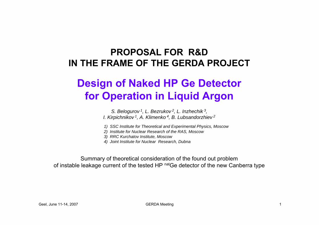
PROPOSAL FOR R&D IN THE FRAME OF THE GERDA PROJECT
Design of Naked HP Ge Detector for Operation in Liquid Argon
S. Belogurov 1, L. Bezrukov 2, L. Inzhechik 3, I. Kirpichnikov 1, A. Klimenko 4, B. Lubsandorzhiev 2
1) SSC Institute for Theoretical and Experimental Physics, Moscow2) Institute for Nuclear Research of the RAS, Moscow3) RRC Kurchatov Institute, Moscow4) Joint Institute for Nuclear Research, Dubna
Summary of theoretical consideration of the found out problem of instable leakage current of the tested HP natGe detector of the new Canberra type
Geel, June 11-14, 2007 GERDA Meeting 2
We can conclude definitely:
The instability of the leakage current of the detector takes place both in liquid nitrogen and in liquid argon if these media are not cleaned.Function of the ‘infrared shield’ is not found out. The increases and decreases of the leakage current has long term character.The exercises carried out during 1.5 year, are followed by both increase and decrease of the leakage current. And there is not a final diagnosis. The refurbishment of the insulator groove results in return of the leakage current to its initial value.Irradiation of the detector under high voltage and of its environment increases the leakage current.Irradiation of the detector without high voltage and of its environment sometimes reduces the leakage current.
There are now more questions than of answers
Status of the problem
Geel, June 11-14, 2007 GERDA Meeting 3
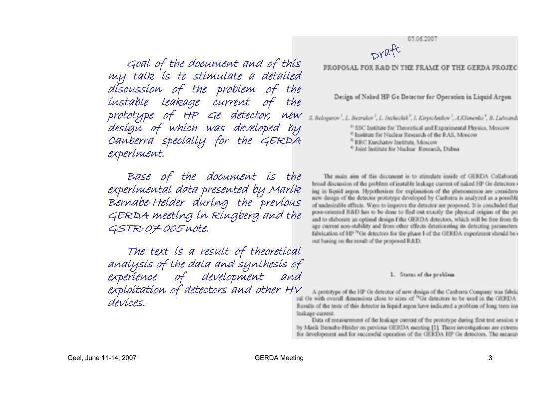
Goal of the document and of this my talk is to stimulate a detailed discussion of the problem of the instable leakage current of the prototype of HP Ge detector, new design of which was developed by Canberra specially for the GERDA experiment.
Base of the document is the experimental data presented by MarikBernabe-Heider during the previous GERDA meeting in Ringberg and the GSTR-07-005 note.
The text is a result of theoretical analysis of the data and synthesis of experience of development and exploitation of detectors and other HV devices.
Draft
Geel, June 11-14, 2007 GERDA Meeting 4
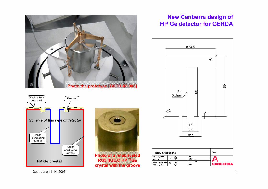
New Canberra design of HP Ge detector for GERDA
SiO2 insulatordeposited
Innerconducting
surface
Groove
Outerconducting
surface
HP Ge HP Ge crystalcrystal
Scheme of this type of detector
Photo of a Photo of a refabricatedrefabricatedRG3 (IGEX) HP RG3 (IGEX) HP 7676Ge Ge
crystal with the groovecrystal with the groove
Photo the prototype [GSTRPhoto the prototype [GSTR--0707--005]005]
Geel, June 11-14, 2007 GERDA Meeting 5
The Canberra detector has open thin insulator inside the narrow (< 4 mm) groove. It is followed by:
1. Collection of charged particles (electrons, ions, impurity clusters) from environing liquid argon and trapping of the charges on the insulator surface contacting with LAr.
2. Electric field of the order of 10 kV/cm in the vicinity of the groove It is more by an order than the field of HP Ge detectors of usual type.
3. Strong non-uniformity of the electric field inside the Ge crystal.
4. A dependence of the electric field upon configuration of outer charges and metal details.
Starting points for explanation of undesirable effects observed and predicted for HP Ge detectors
of the new Canberra design
Geel, June 11-14, 2007 GERDA Meeting 6
1. Collection of charged particles on the insulator made of good dielectric material results usually in sporadic micro-discharges along the insulator surface. The discharges cause:
light flashes; direct leakage current;pulse leakage current generating electromagnetic noise;chemical modification of the insulator surface followed by surface conductivity and, accordingly, by extra direct leakage current.
2. Electric field of 10 kV/cm stimulates the collection and trapping of the charges. Also this unusually high field intensifies the micro-discharges.
3. Non-uniformity of the electric field inside the Ge crystal leads to difference of transport conditions for charge carriers in the Ge crystal. Shape of output pulses and efficiency of collection of the quasi-electrons and holes depends on location of an energy deposition. Uselessness of the pulse shape analysis and bad energy resolution can be results of it.
4. Dependence of the electric field upon configuration of outer charges and metal details leads to an uncertainty of parameters of the detector.
Phenomena following the effects
Geel, June 11-14, 2007 GERDA Meeting 7
The experiments carried out with Co-60 gamma source are in accordance with the hypothesis of collection charges from the LAr and trapping of the charges on the insulator surface:
1. Irradiation leads to creation in the LAr of a conductive cloud of electrons and ions.
2. Under high voltage applied the charges are collected and trapped. There are conditions for the micro-discharges.
3. Without HV the charges can run off the insulator surface or can be recombinated.
4. To confirm the statement the conductivity of the irradiated LArshould be estimated.
Experiments on irradiation of the detector and LArby the ionizing source are in accordance with the supposition of charges on the insulator surface
Geel, June 11-14, 2007 GERDA Meeting 8
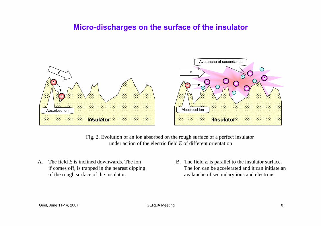
Micro-discharges on the surface of the insulator
+
E
+
Insulator
Absorbed ion
─
E
+ ++
+
+
+
─
─
─
─
─
Avalanche of secondaries
+
Insulator
Absorbed ion
B. The field E is parallel to the insulator surface. The ion can be accelerated and it can initiate an avalanche of secondary ions and electrons.
A. The field E is inclined downwards. The ion if comes off, is trapped in the nearest dippingof the rough surface of the insulator.
Fig. 2. Evolution of an ion absorbed on the rough surface of a perfect insulatorunder action of the electric field E of different orientation
Geel, June 11-14, 2007 GERDA Meeting 9
Usual starting points for designing detectors and any other devices of high voltage
1. Effect of collection and trapping of the charge particles (electrons and ions) on the surface of the insulator should be taken into account. 1.1. The better dielectric material of the insulator, the longer time (up to
weeks) of presence of the charges on the insulator surface.1.2. The electric field should be non-parallel to the insulator surface.
2. The electrostatic field inside the devices should be closed. All outer surfaces of the device should have fixed potential. It provides:2.1. Absence of the trapped extra charges on the surfaces.2.2. Prevention of the micro-discharges.2.3. Fixation of a nominal geometry of internal electro-static field to avoid
a dependence of the field on the configuration of the metal environment.
These requirements are met usually both by application of a special geometry of the insulators and by a covering of the insulator by weakly conductive
layer or by an using of bad insulating material
Extra starting point for designing HV devices for operation in the liquid argon:
Electrons and ions born in LAr have extreme high survivability.
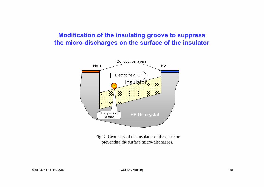
Geel, June 11-14, 2007 GERDA Meeting 10
Electric field E
Conductive layersHV + HV ─
+
HP Ge HP Ge crystalcrystalTrapped ionis fixed
Fig. 7. Geometry of the insulator of the detectorpreventing the surface micro-discharges.
Modification of the insulating groove to suppress the micro-discharges on the surface of the insulator
Insulator
Geel, June 11-14, 2007 GERDA Meeting 11
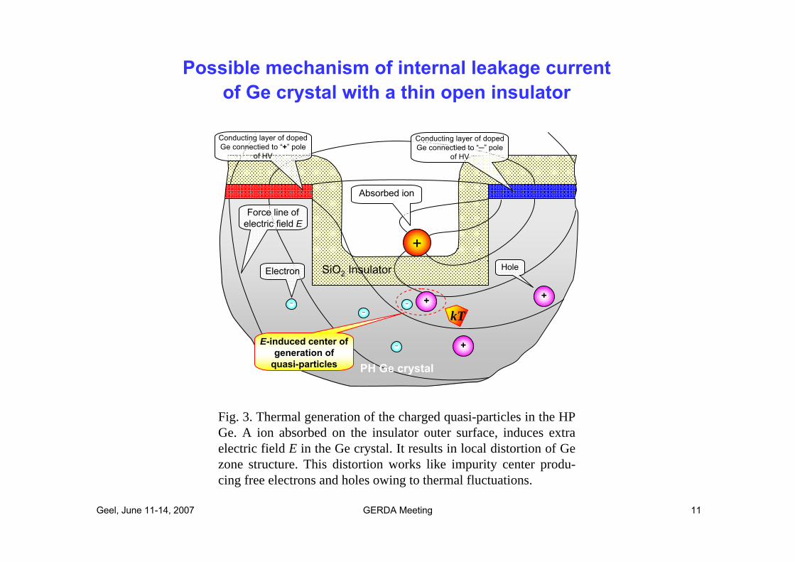
Possible mechanism of internal leakage current of Ge crystal with a thin open insulator
Fig. 3. Thermal generation of the charged quasi-particles in the HP Ge. A ion absorbed on the insulator outer surface, induces extraelectric field E in the Ge crystal. It results in local distortion of Ge zone structure. This distortion works like impurity center produ-cing free electrons and holes owing to thermal fluctuations.
PH Ge PH Ge crystalcrystal
Conducting layer of dopedGe connectied to “+” pole
of HV
Conducting layer of dopedGe connectied to “─” pole
of HV
+
─
─
─
─ + +
+
Absorbed ion
E-induced center ofgeneration of
quasi-particles
HoleElectron
Force line ofelectric field E
SiO2 Insulator
kT
Geel, June 11-14, 2007 GERDA Meeting 12
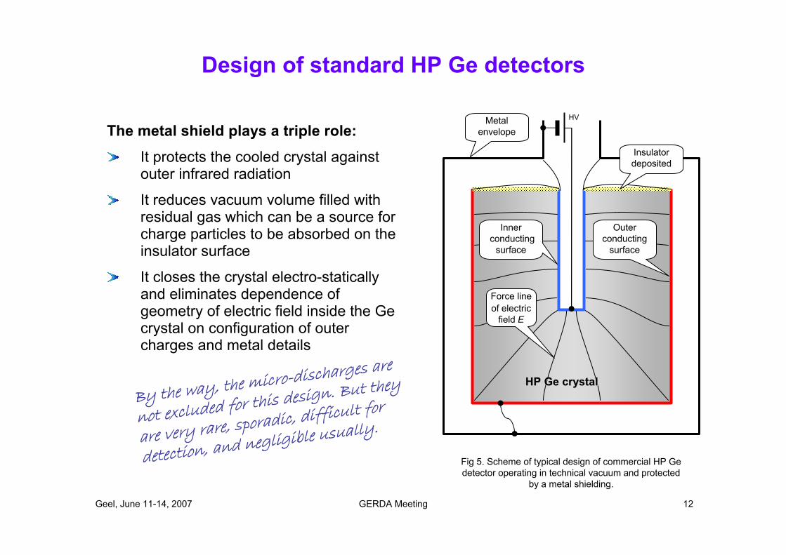
Design of standard HP Ge detectors
The metal shield plays a triple role:
It protects the cooled crystal against outer infrared radiation
It reduces vacuum volume filled with residual gas which can be a source for charge particles to be absorbed on the insulator surface
It closes the crystal electro-statically and eliminates dependence of geometry of electric field inside the Ge crystal on configuration of outer charges and metal details
Innerconducting
surface
Outerconducting
surface
Insulatordeposited
Metalenvelope
HV
HP Ge HP Ge crystalcrystal
Force lineof electric
field E
Fig 5. Scheme of typical design of commercial HP Ge detector operating in technical vacuum and protected
by a metal shielding.
By the way, the micro-discharges are
not excluded for this design. But they
are very rare, sporadic, difficult for
detection, and negligible usually.
Geel, June 11-14, 2007 GERDA Meeting 13
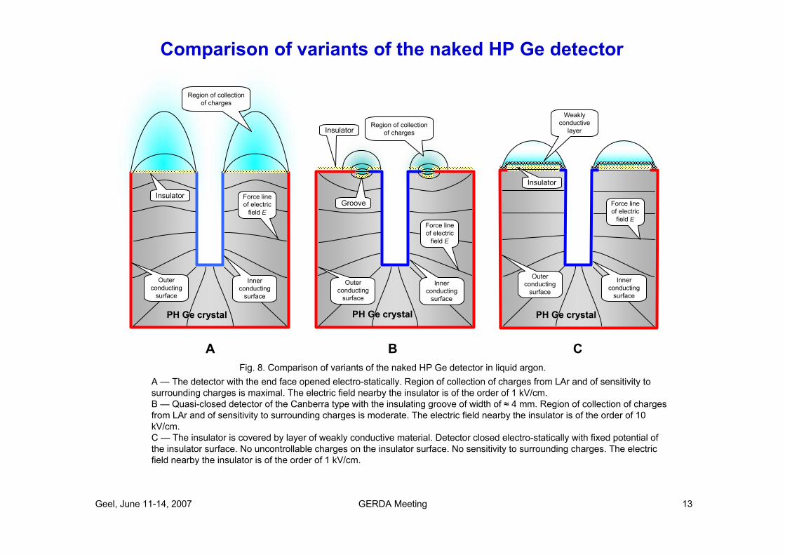
Comparison of variants of the naked HP Ge detector
Outerconducting
surface
Innerconducting
surface
PH Ge PH Ge crystalcrystal
Force lineof electric
field E
Insulator
Region of collectionof charges
PH Ge PH Ge crystalcrystal
Region of collectionof charges
Force lineof electric
field E
Outerconducting
surface
Innerconducting
surface
Insulator
Groove
PH Ge PH Ge crystalcrystal
Outerconducting
surface
Innerconducting
surface
Force lineof electric
field E
Insulator
Weaklyconductive
layer
A B CFig. 8. Comparison of variants of the naked HP Ge detector in liquid argon.
A — The detector with the end face opened electro-statically. Region of collection of charges from LAr and of sensitivity tosurrounding charges is maximal. The electric field nearby the insulator is of the order of 1 kV/cm.B — Quasi-closed detector of the Canberra type with the insulating groove of width of ≈ 4 mm. Region of collection of chargesfrom LAr and of sensitivity to surrounding charges is moderate. The electric field nearby the insulator is of the order of 10 kV/cm.C — The insulator is covered by layer of weakly conductive material. Detector closed electro-statically with fixed potential ofthe insulator surface. No uncontrollable charges on the insulator surface. No sensitivity to surrounding charges. The electricfield nearby the insulator is of the order of 1 kV/cm.
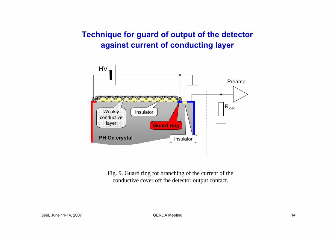
Geel, June 11-14, 2007 GERDA Meeting 14
HV
PH Ge PH Ge crystalcrystal Insulator
Guard ring
Weaklyconductive
layer
Insulator
Preamp
Rload
Fig. 9. Guard ring for branching of the current of the conductive cover off the detector output contact.
Technique for guard of output of the detector against current of conducting layer
Geel, June 11-14, 2007 GERDA Meeting 15
Conclusions
1. The observed instability of the leakage current of the tested PH Ge detector is caused rather probably by collection of charges from LAr and trapping of the charges on the insulator surface of the groove, that leads, in turn, to the micro-discharges on the insulator.
2. The effect seems to be intrinsic for the new Canberra design of the detector. The design can create the extra problems of the detector efficiency, of its energy resolution, and of use ofthe pulse shape analysis.
3. We propose to carry out the R&D work to study physics of the observed phenomena and to optimize the design of the HP Ge detectors for the Phase I of the GERDA experiment.
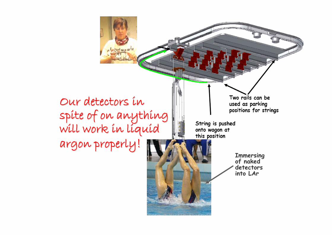
Immersing of naked detectors into LAr
Our detectors in Our detectors in spite of on anythingspite of on anythingwill work in liquid will work in liquid argon properlyargon properly!!