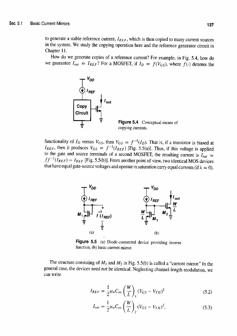
Embed Size (px)
Citation preview


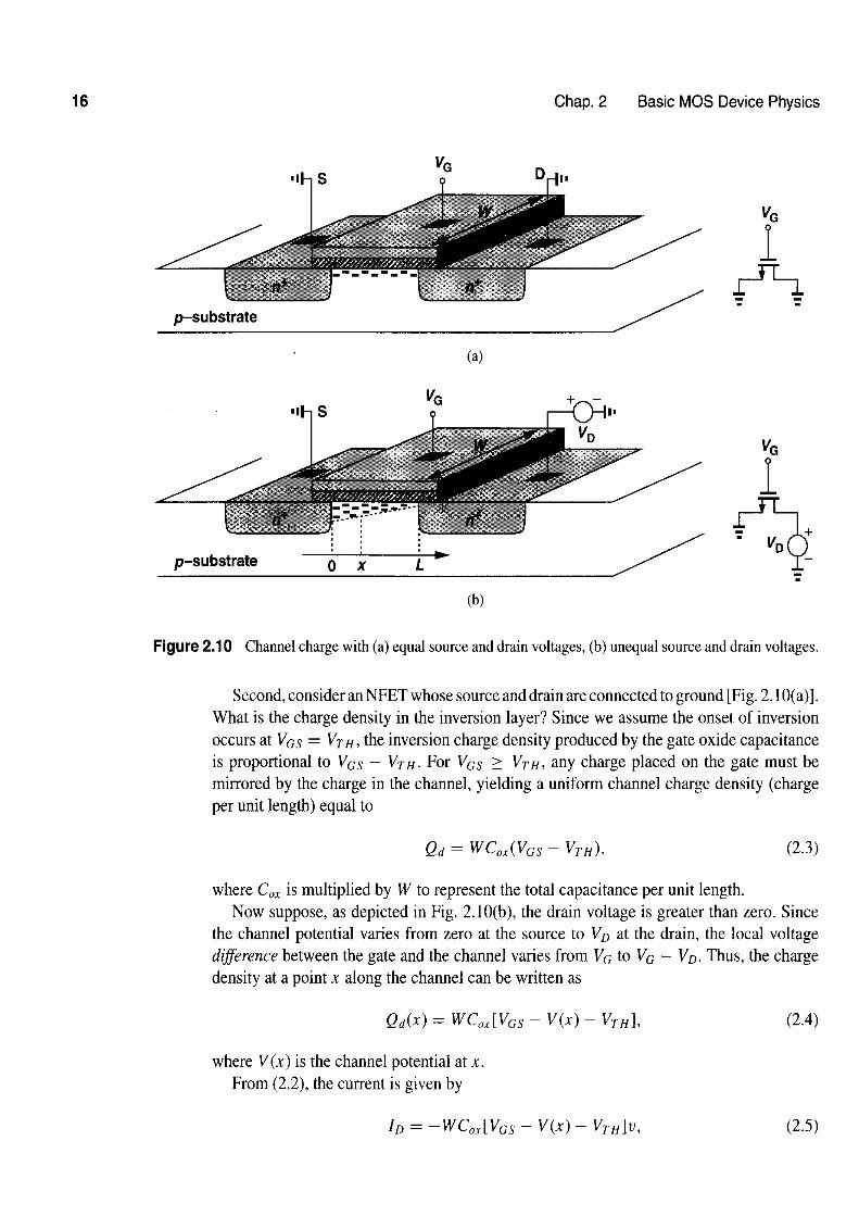
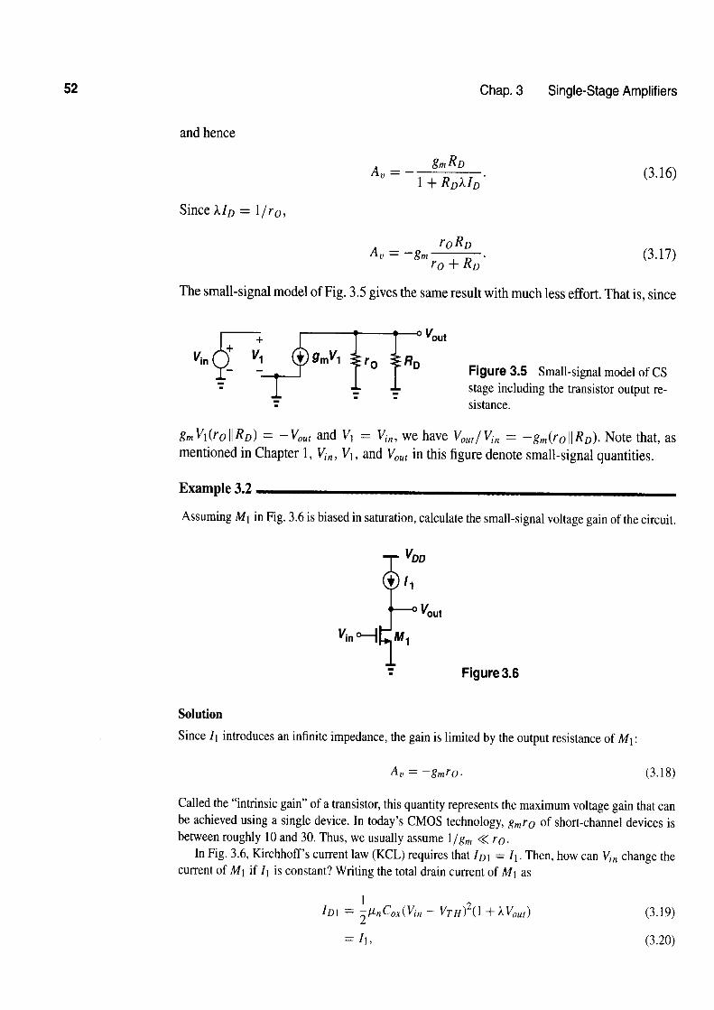
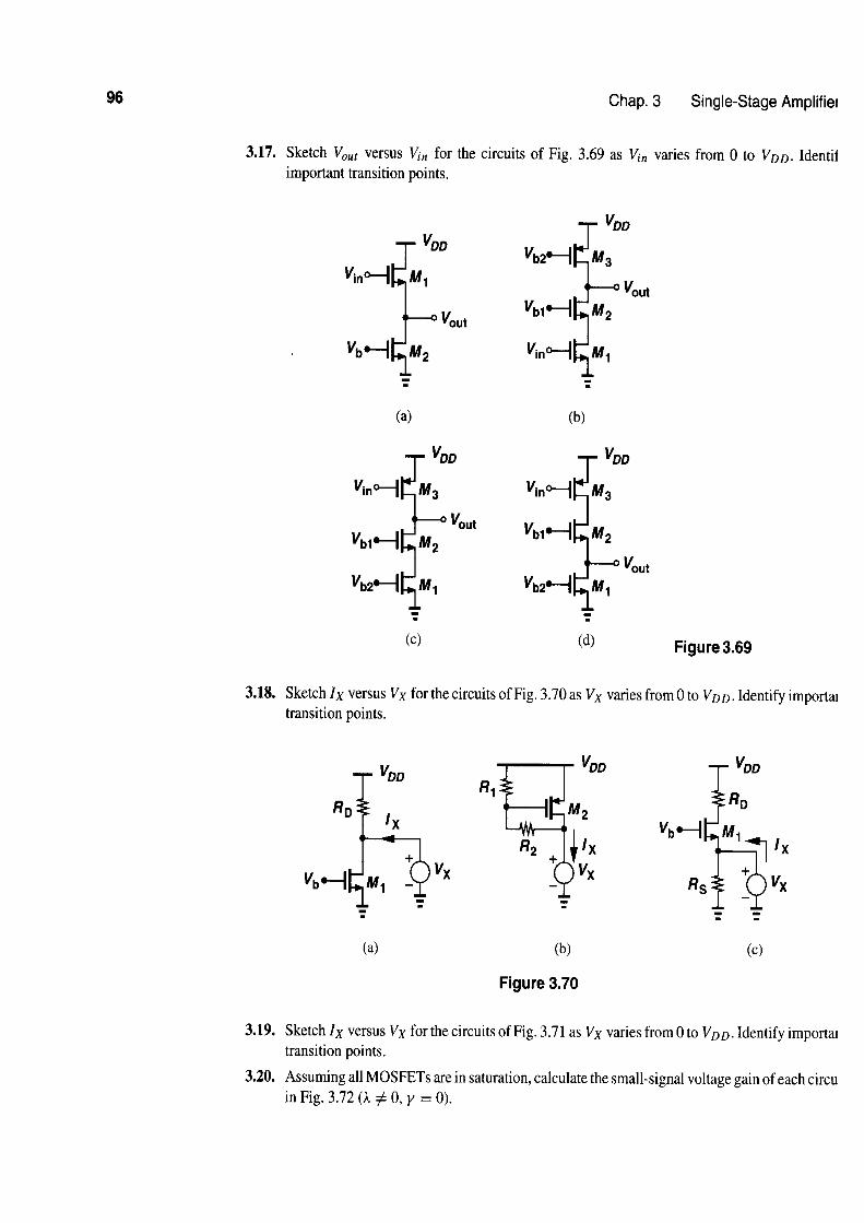
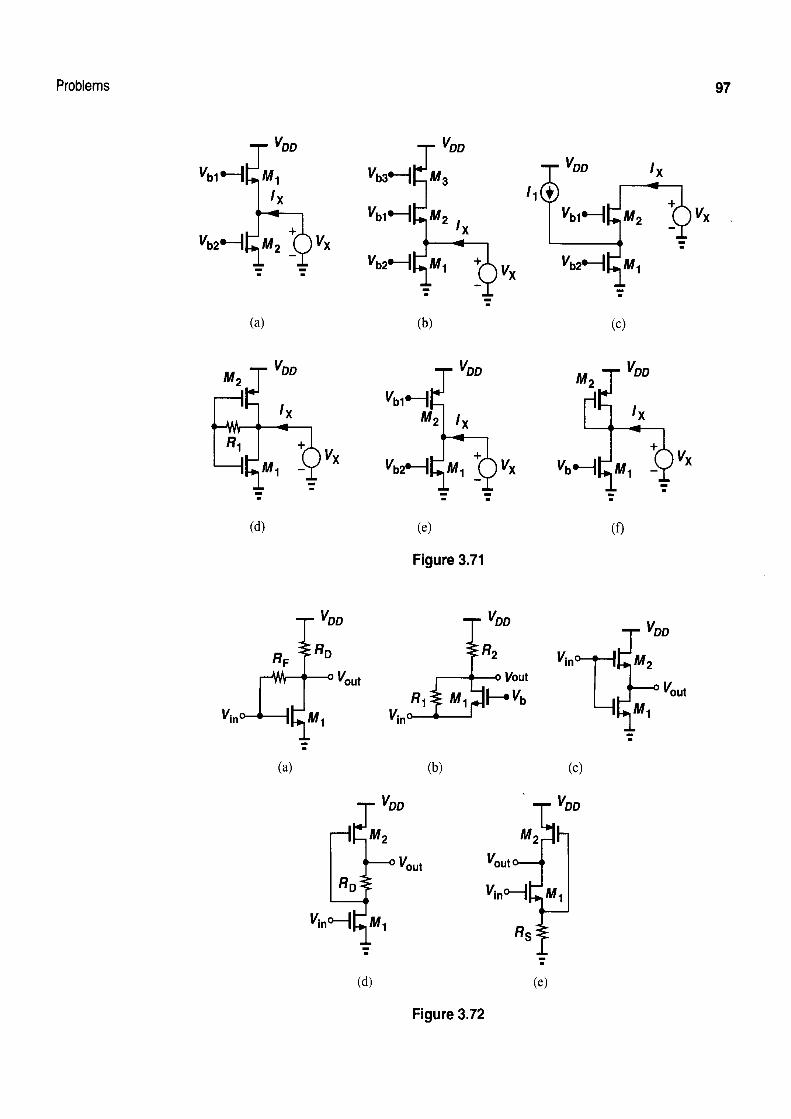
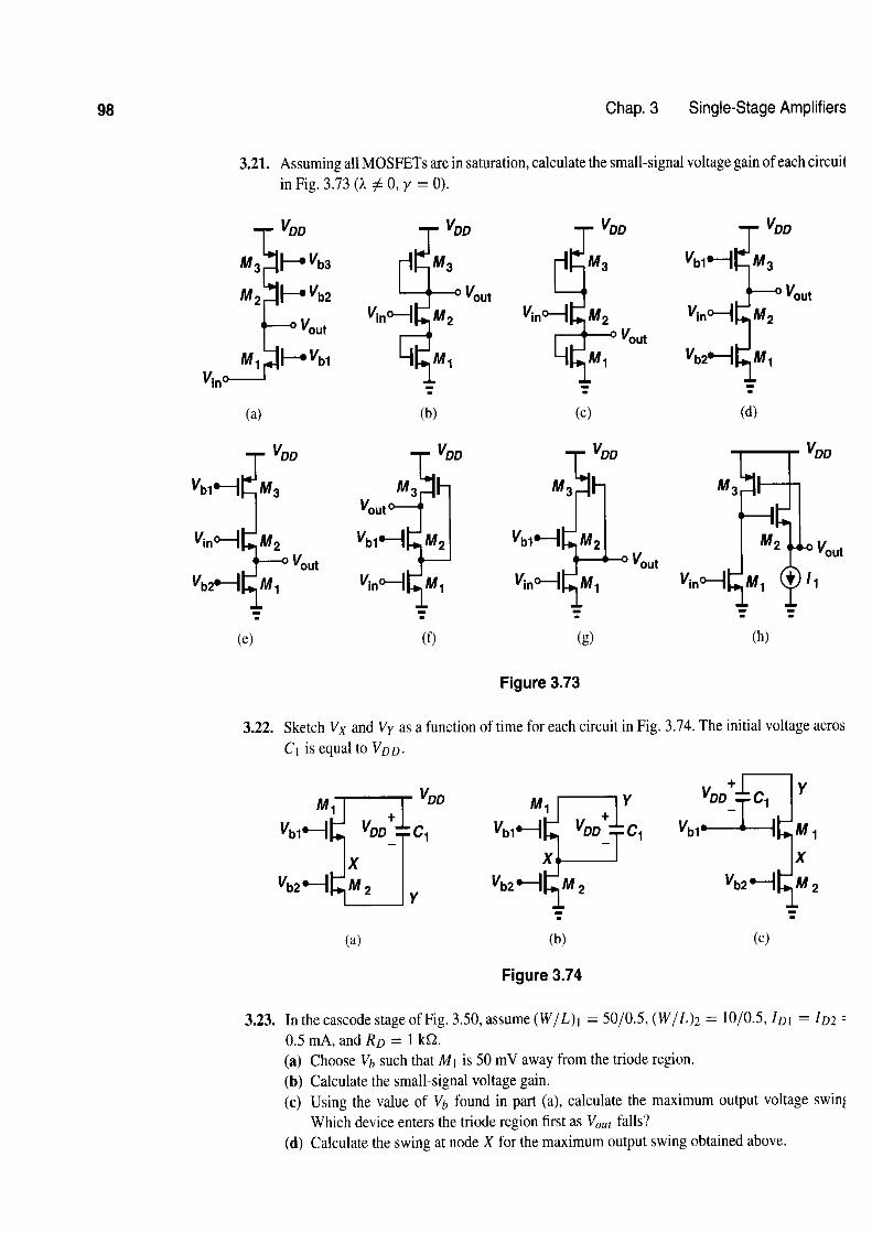
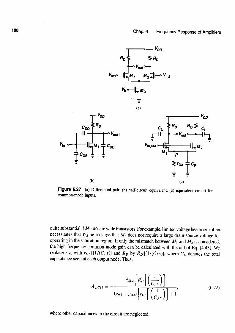
Chap. 3 Single-Stage Amplifiers
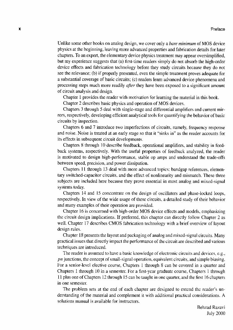
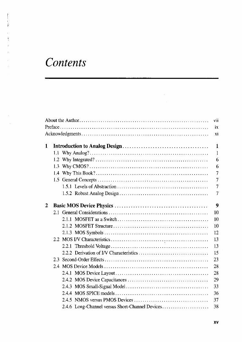
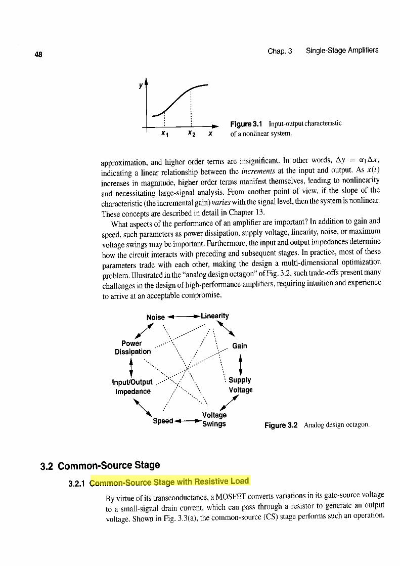
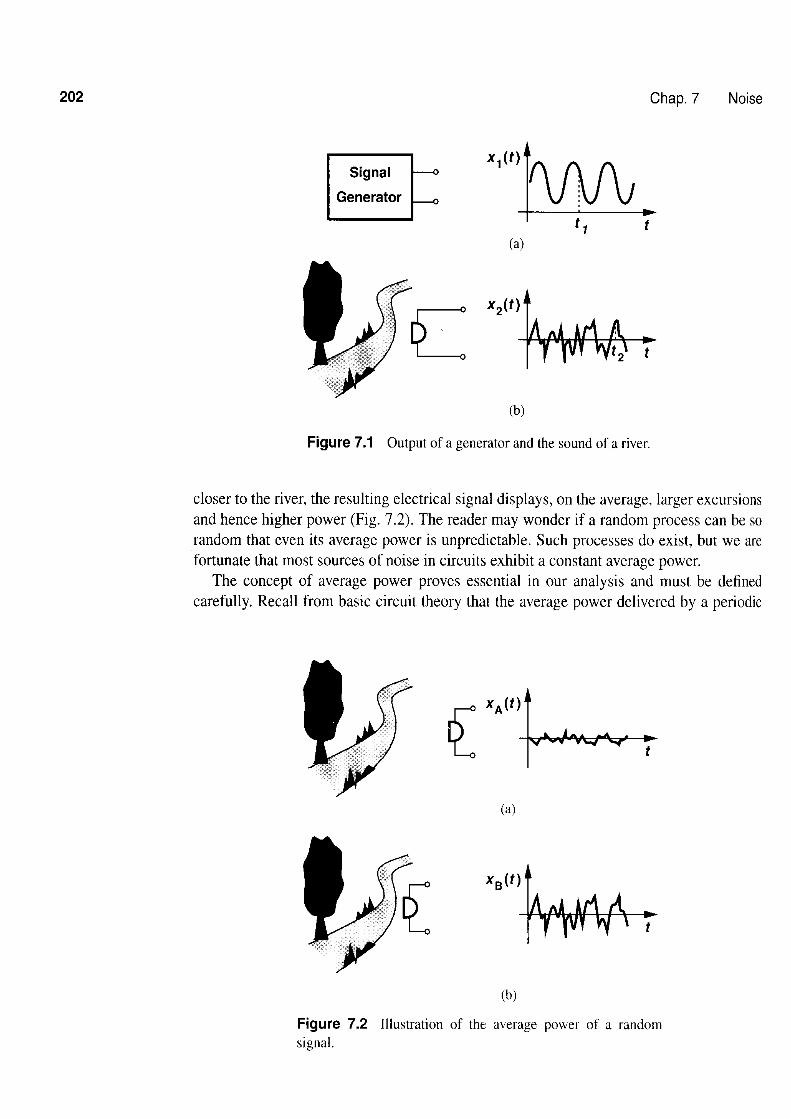
I Figure 3.1 Input-output characteristic X1 X 2 X of a nonlinear system.
approximation, and higher order terms are insignificant. In other words, Ay = a1 Ax, indicating a linear relationship between the increments at the input and output. As x ( t )
increases in magnitude, higher order terms manifest themselves, leading to nonlinearity and necessitating large-signal analysis. From another point of view, if the slope of the characteristic (the incremental gain) varies with the signal level, then the system is nonlinear. These concepts are described in detail in Chapter 13.
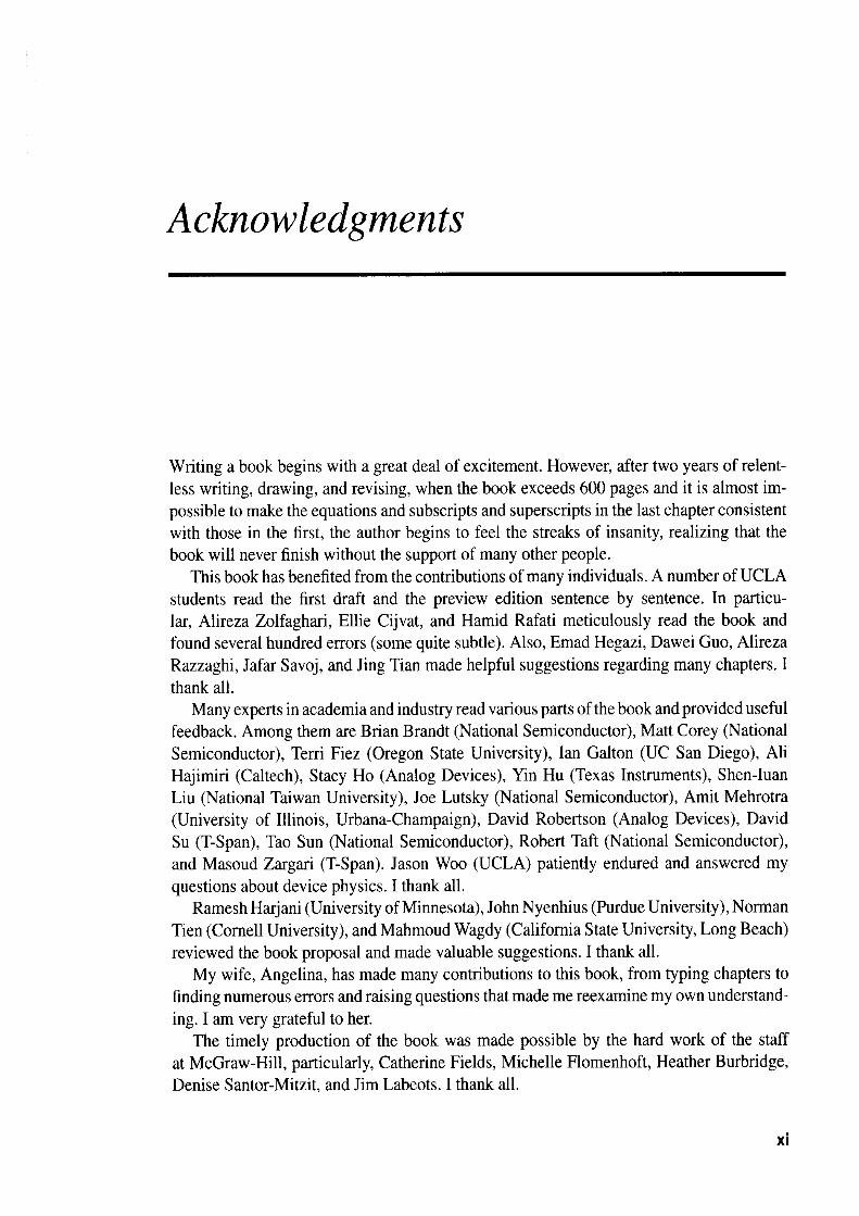
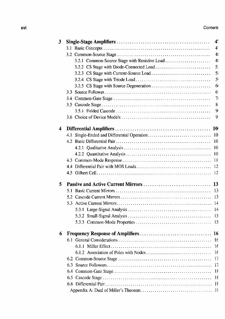
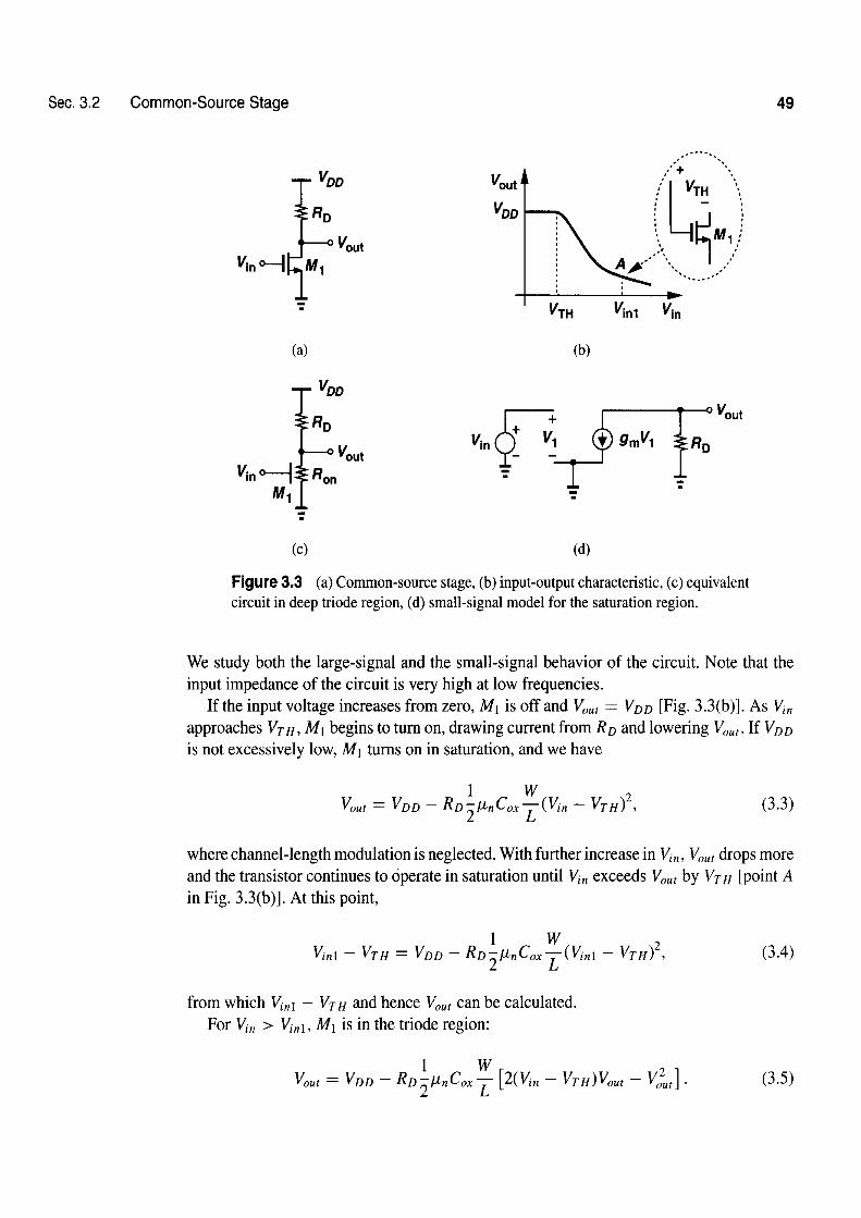
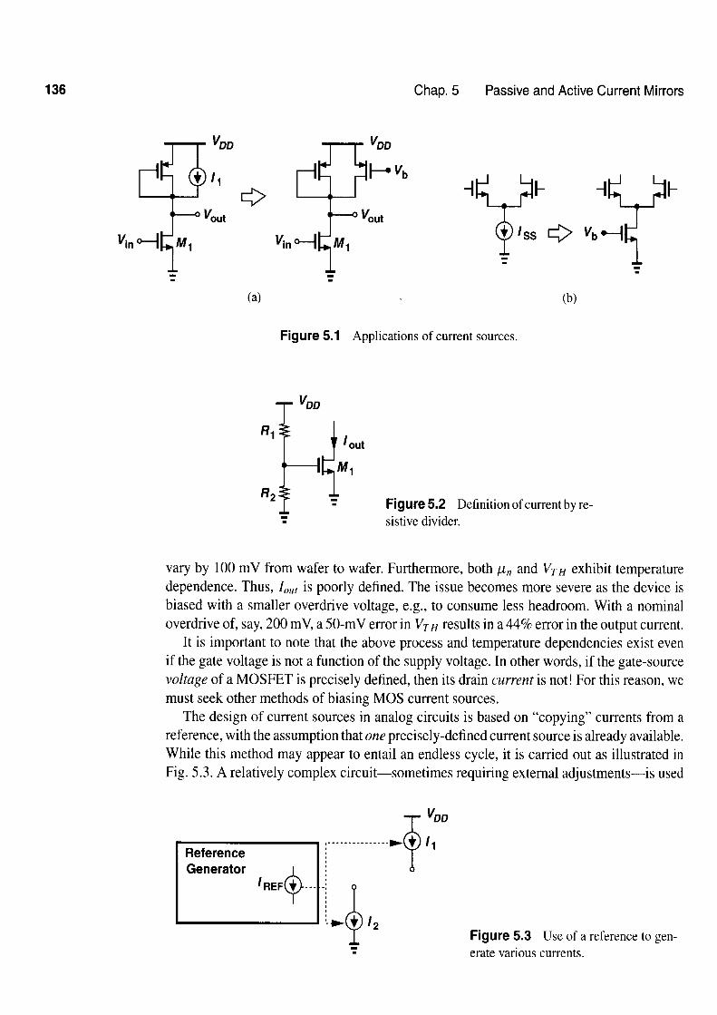
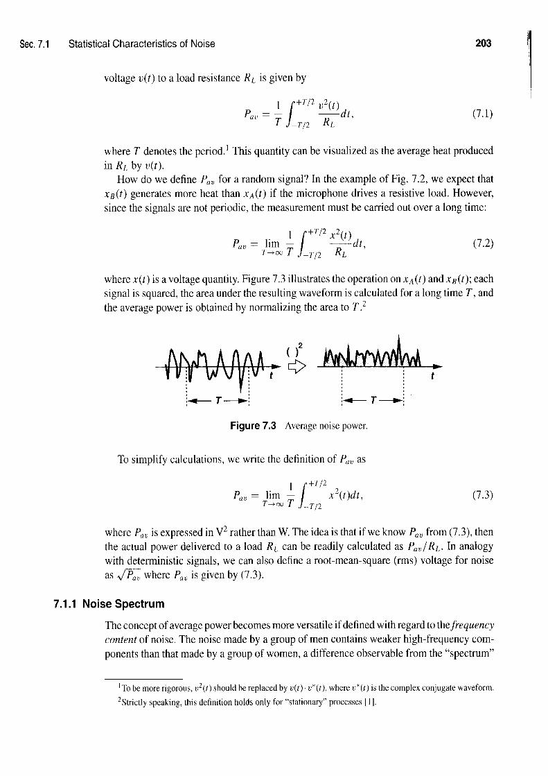
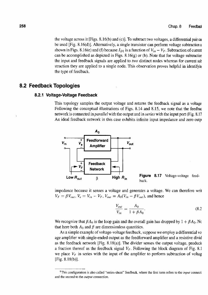
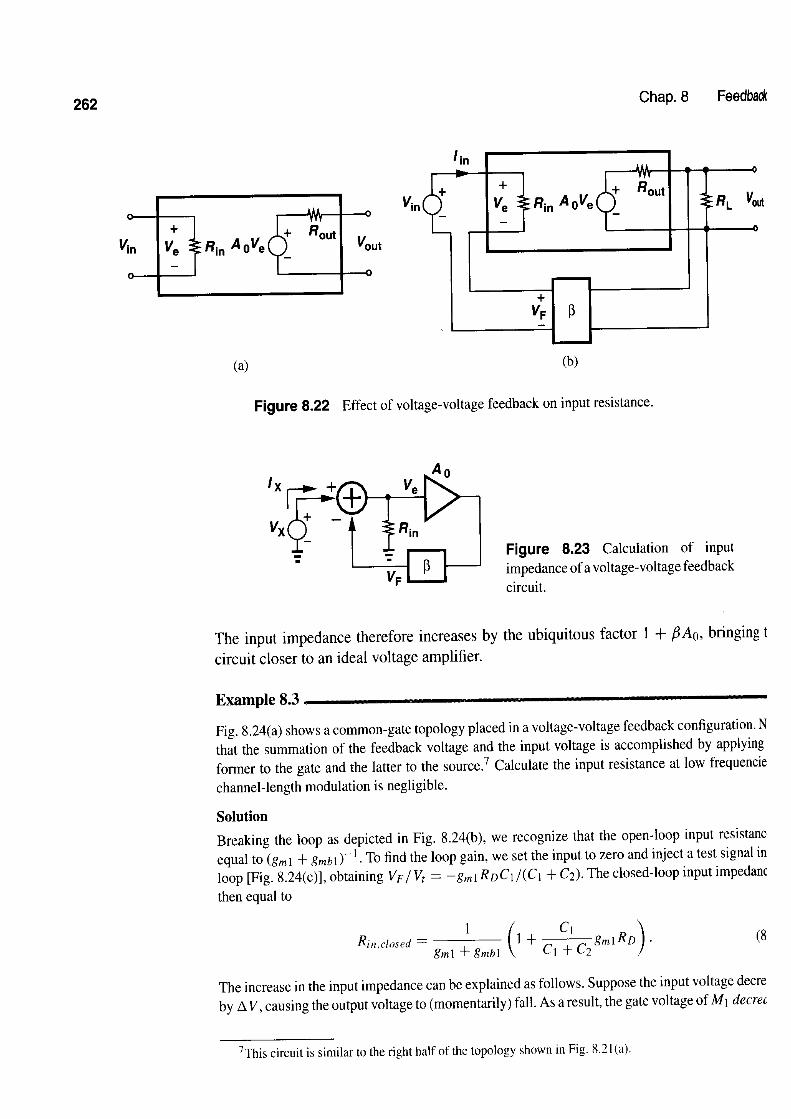
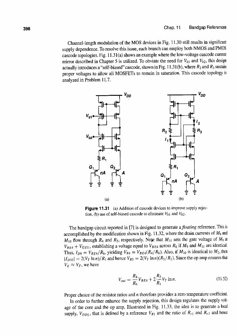
What aspects of the performance of an amplifier are important? In addition to gain and speed, such parameters as power dissipation, supply voltage, linearity, noise, or maximum voltage swings may be important. Furthermore, the input and output impedances determine how the circuit interacts with preceding and subsequent stages. In practice, most of these parameters trade with each other, making the design a multi-dimensional optimization problem. Illustrated in the "analog design octagon" of Fig. 3.2, such trade-offs present many challenges in the design of high-performance amplifiers, requiring intuition and experience to arrive at an acceptable compromise.
Noise -Linearity
/f '%; . .-* .-*+- ' , ; ; L \ '. ..-. :* - - ,' -,
Power +..- ., , a
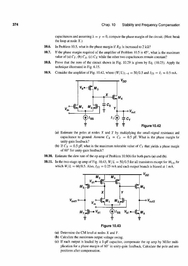
I - - Dissipation Gain . ,*+- . . . ' *...+'I
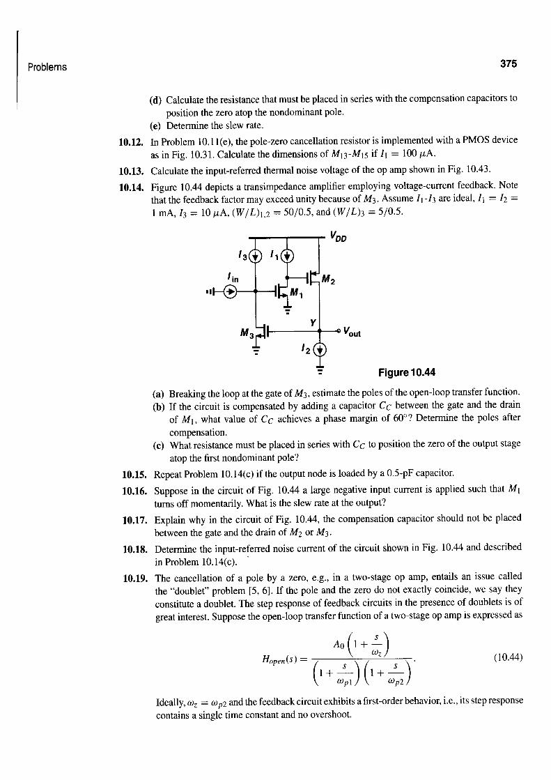
I, ,',,.-+* -.... . :*,- .;, I*.. .....,, .\
InputIOutput ...--":.. , , ,' ',$.
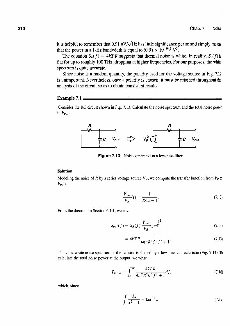
; t : Supply
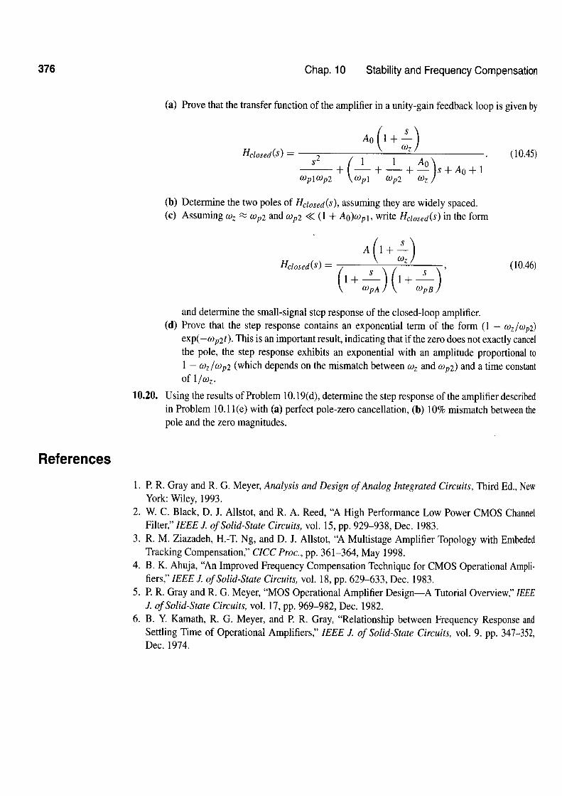
,'*. Impedance , . , '. *
. 4 . . s \ ,;
', ' . . . L
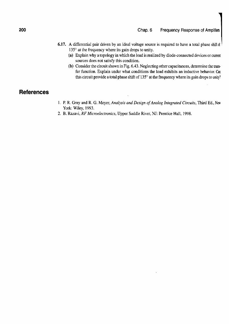
' Voltage . Ytage Speed-~wings Figure 3.2 Analog design octagon.
3.2 Common-Source Stage
3.2.1 Common-Source Stage with Resistive Load
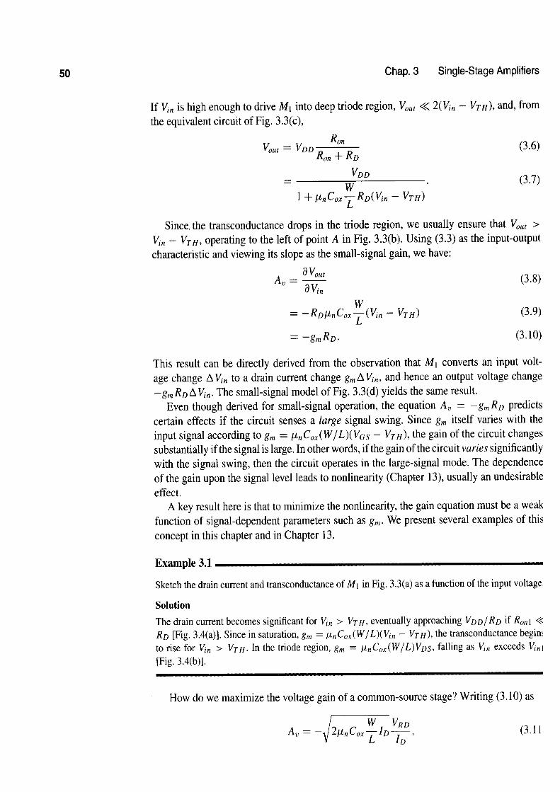
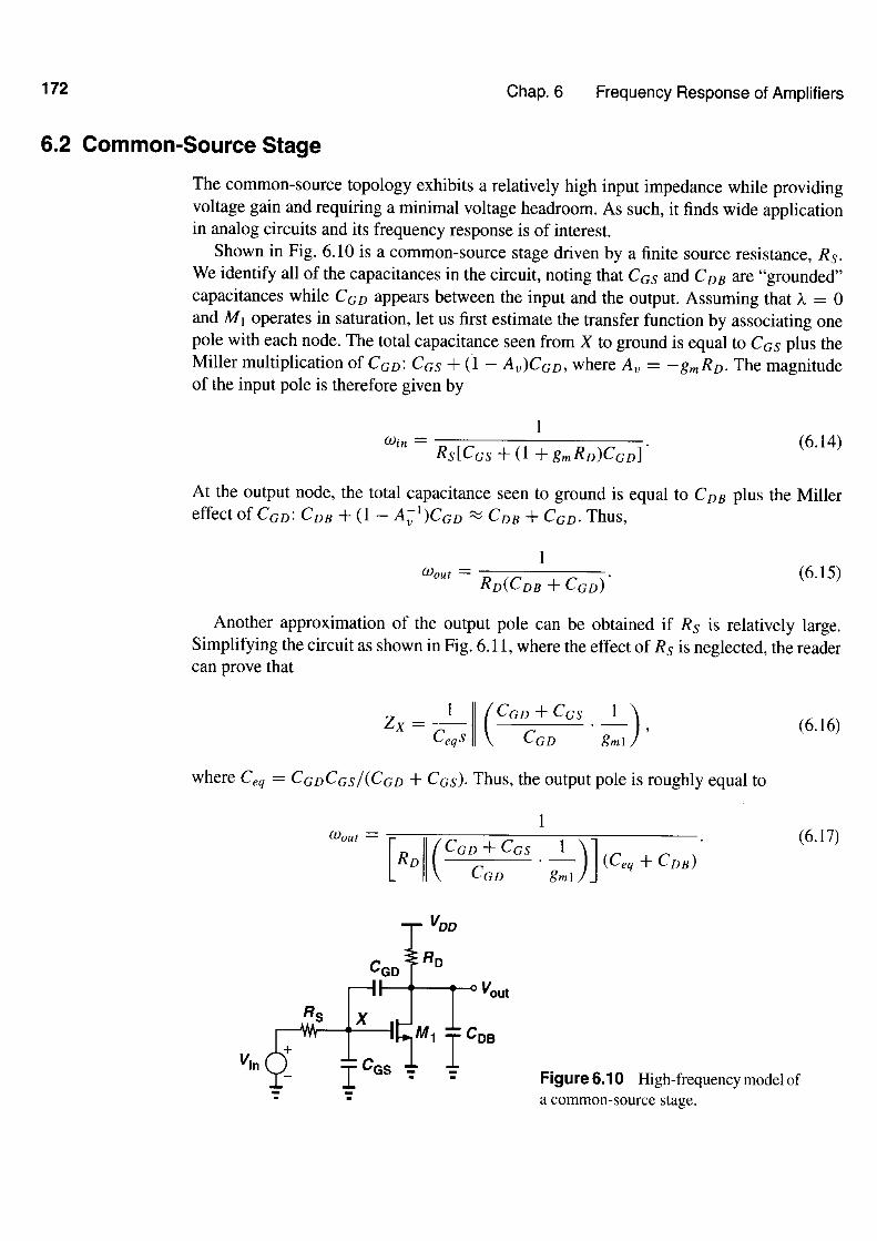
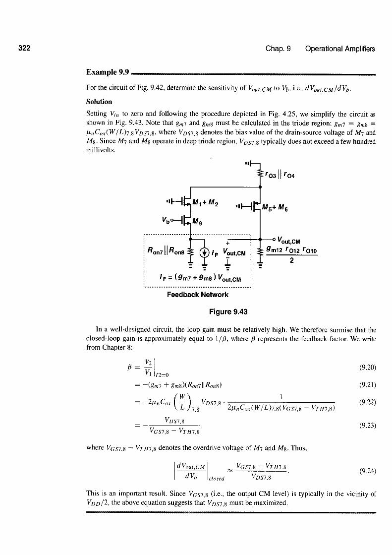
By virtue of its transconductance, a MOSFET converts variations in its gate-source voltage to a small-signal drain current, which can pass through a resistor to generate an output voltage. Shown in Fig. 3.3(a), the common-source (CS) stage performs such an operation.
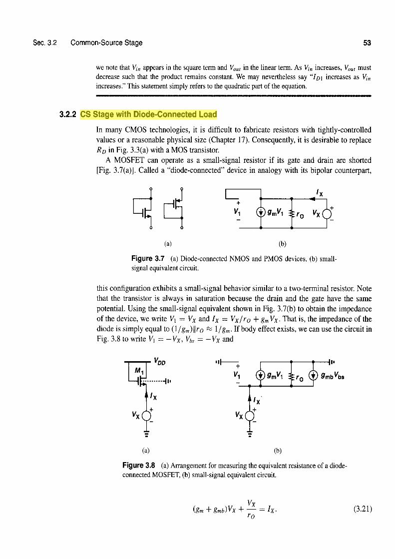
Sec. 3.2 Common-Source Stage 53
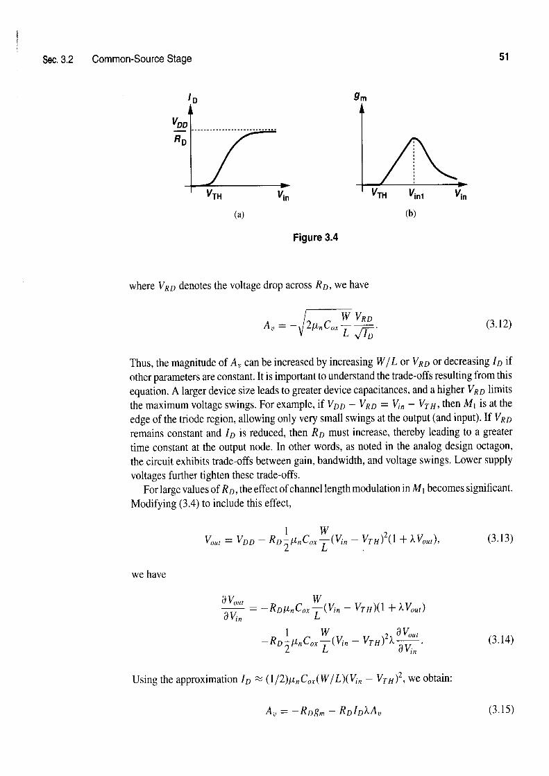
we note that Vin appears in the square term and VOUt in the linear term. As Vin increases, VOUt must decrease such that the product remains constant. We may nevertheless say "ID1 increases as Vin increases." This statement simply refers to the quadratic part of the equation.
3.2.2 CS Stage with Diode-Connected Load
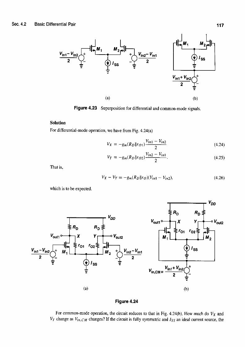
In many CMOS technologies, it is difficult to fabricate resistors with tightly-controlled values or a reasonable physical size (Chapter 17). Consequently, it is desirable to replace R D in Fig. 3.3(a) with a MOS transistor.
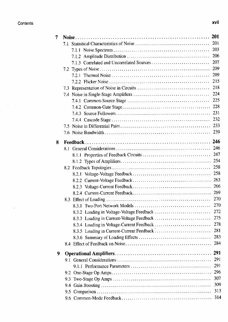
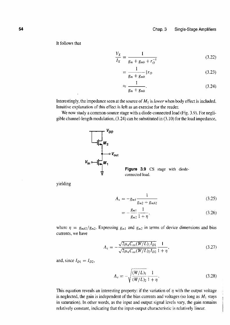
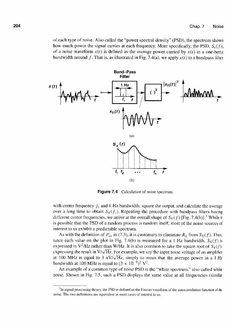
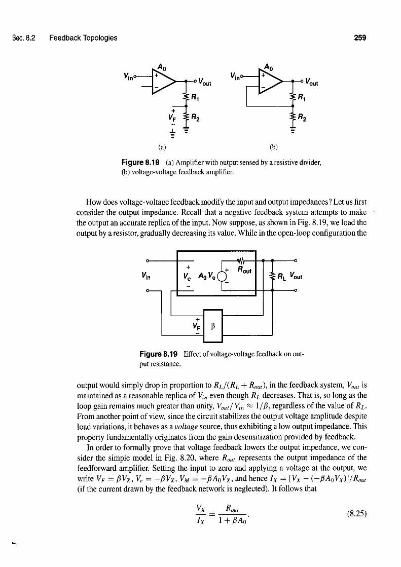
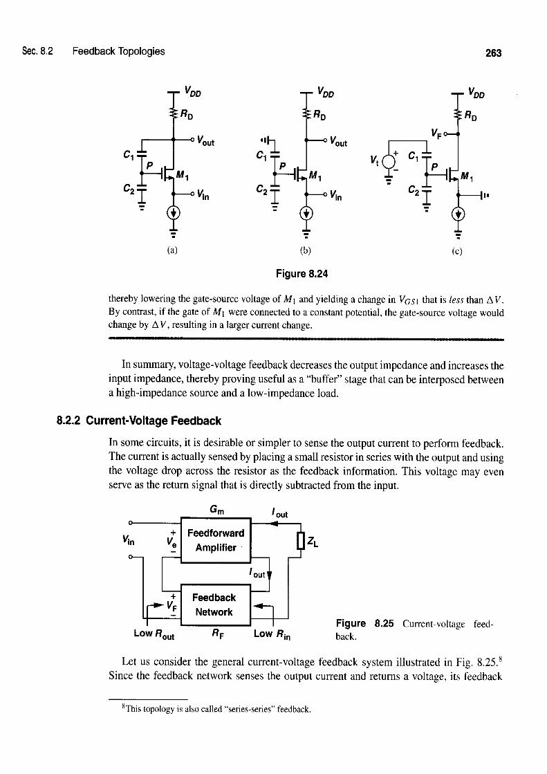
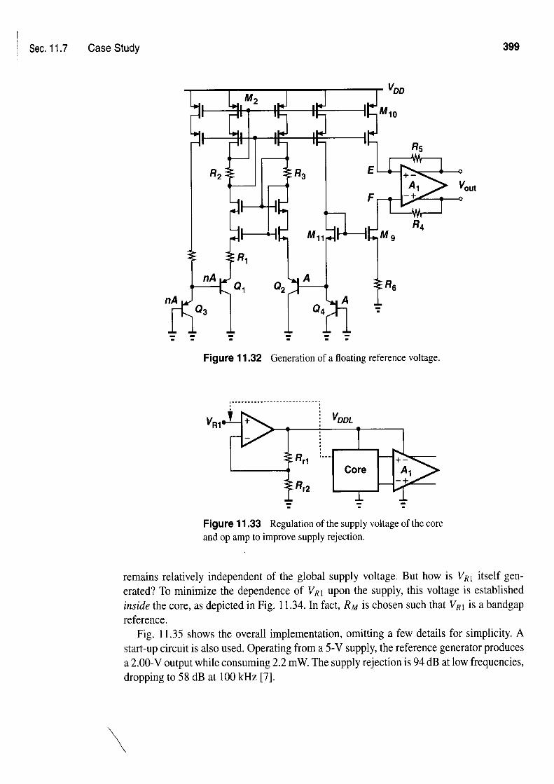
A MOSFET can operate as a small-signal resistor if its gate and drain are shorted [Fig. 3.7(a)]. Called a "diode-connected" device in analogy with its bipolar counterpart,
(a) (b)
Figure 3.7 (a) Diode-connected NMOS and PMOS devices, (b) small- signal equivalent circuit.
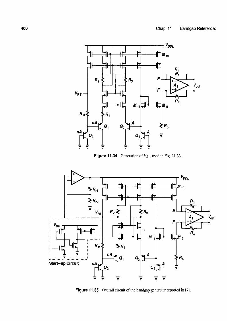
this configuration exhibits a small-signal behavior similar to a two-terminal resistor. Note that the transistor is always in saturation because the drain and the gate have the same potential. Using the small-signal equivalent shown in Fig. 3.7(b) to obtain the impedance of the device, we write Vl = Vx and Ix = Vx/ro + g, Vx. That is, the impedance of the diode is simply equal to ( I /g,) ltro = 1 / g m . If body effect exists, we can use the circuit in Fig. 3.8 to write Vl = -Vx, Vbs = -VX and
Figure 3.8 (a) Arrangement for measuring the equivalent resistance of a diode- connected MOSFET, (b) small-signal equivalent circuit.
Chap. 3 Single-Stage Amplifiers
Moreover,
yielding
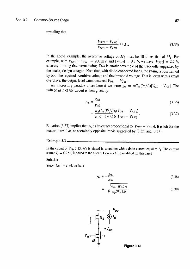
Thus, for a gain of 10, the overdrive of M2 need be only 2.5 times that of M I . Alternatively, for a given overdrive voltage, this circuit. achieves a gain four times that of the stage in Fig. 3.12. Intuitively, this is because for a given (VGS2 - VTH2(, if the current decreases by a factor of 4, then ( W / L ) 2 must decrease proportionally, and g,2 = J 2 p p C o x ( ~ / ~ ) 2 ~ D 2 is lowered by the same factor.
We should also'mention that in today's CMOS technology, channel-length modulation is quite significant and, more importantly, the behavior of transistors notably departs from the square law (Chapter 16). Thus, the gain of the stage in Fig. 3.9 must be expressed as
where g, 1 and g,:! must be obtained as described in Chapter 16.
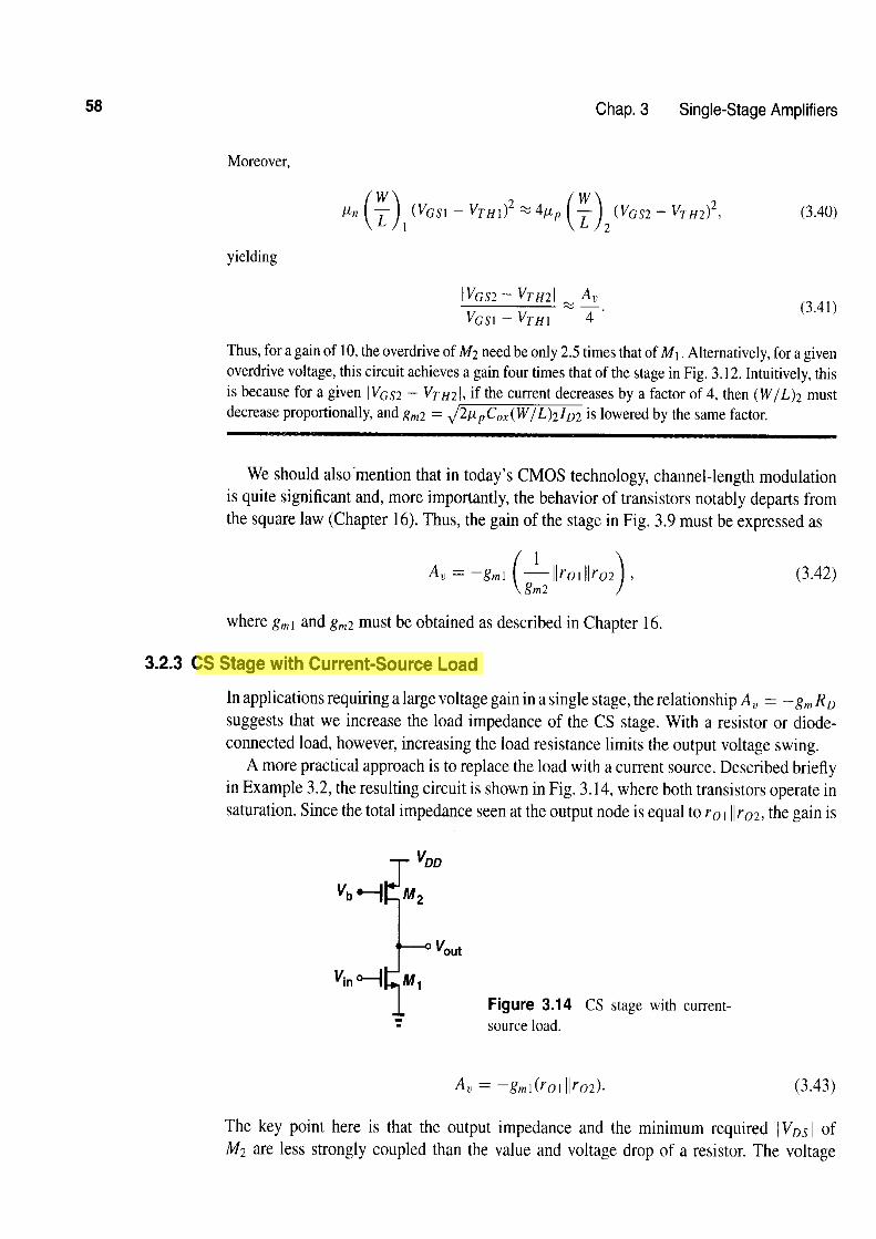
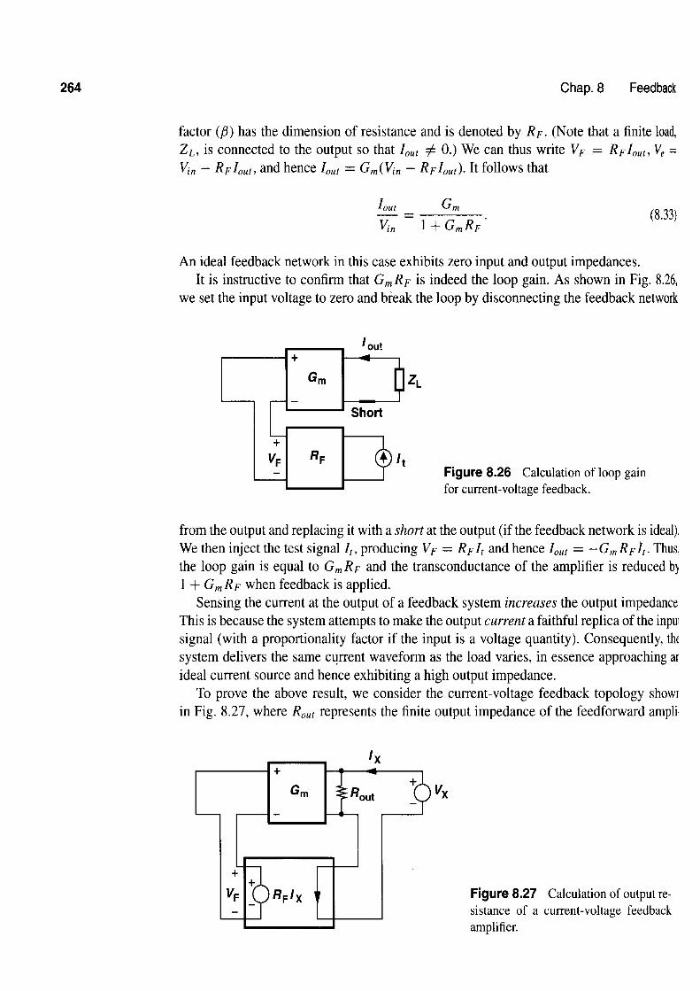
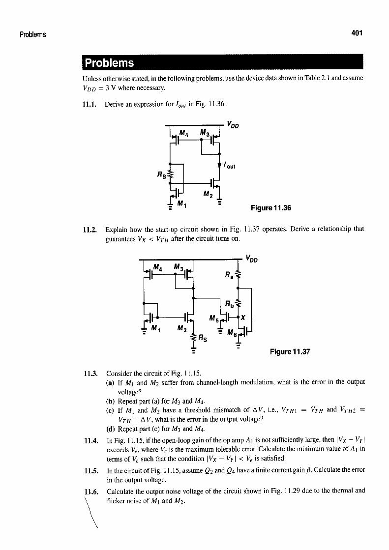
3.2.3 CS Stage with Current-Source Load
In applications requiring alarge voltage gain in a single stage, the relationship A, = -g, RD suggests that we increase the load impedance of the CS stage. With a resistor or diode- connected load, however, increasing the load resistance limits the output voltage swing.
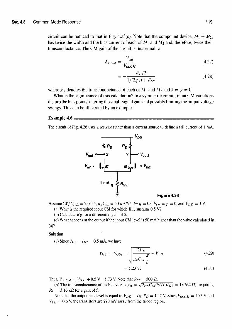
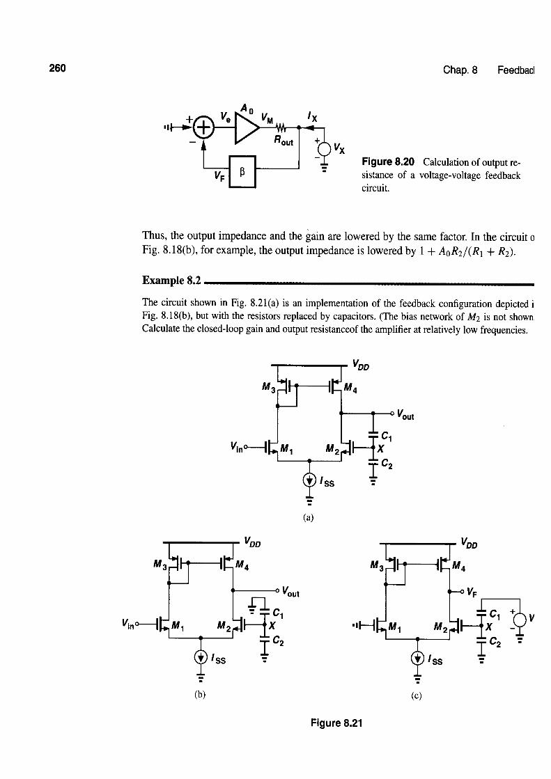
A more practical approach is to replace the load with a current source. Described briefly in Example 3.2, the resulting circuit is shown in Fig. 3.14, where both transistors operate in saturation. Since the total impedance seen at the output node is equal to rol Ilro2, the gain is
Figure 3.14 CS stage with current- - source load.
The key point here is that the output impedance and the minimum required lVnsl of Mz are less strongly coupled than the value and voltage drop of a resistor, The voltage
Sec. 3.2 Common-Source Stage 59
I vDS2,rnin I = I VGS2 - VTH21 can be reduced to even a few hundred millivolts by simply increasing the width of M2. If r-02 is not sufficiently high, the length and width of M2 can be increased to achieve a smaller A while maintaining the same overdrive voltage. The penalty is the large capacitance introduced by M2 at the output node.
We should remark that the output bias voltage of the circuit in Fig. 3.14 is not well- defined. Thus, the stage is reliably biased only if a feedback loop forces V,,, to a known value (Chapter 8). The large-signal analysis of the circuit is left as an exercise for the reader.
As explained in Chapter 2, the output impedance of MOSFETs at a given drain current can be scaled by changing the channel length, i.e., to the first order, h a 1/L and hence ro a LIZD. Since the gain of the stage shown in Fig. 3.14 is proportional to r01 llrO2, we may surmise that longer transistors yield a higher voltage gain.
Let us consider MI and M2 separately. If L 1 is scaled by a factor a (> I), then Wl may need to be scaled proportionally as well. This is because, for a given drain current, VGsi - V T H l a l / J m , i.e., if W1 is not scaled, the overdrive voltage increases, limiting the output voltage swing. Also, since g,l a d m , scaling up only L1 lowers g,,.
In applications where these issues are unimportant, Wl can remain constant while L 1 increases. Thus, the intrinsic gain of the transistor can be written as
indicating that the gain increases with L because h depends more strongly on L than g, does. Also, note that g,ro decreases as ID increases.
Increasing L2 while keeping W2 constant increases ro2 and hence the voltage gain, but at the cost of higher I VDS21 required to maintain M2 in saturation.
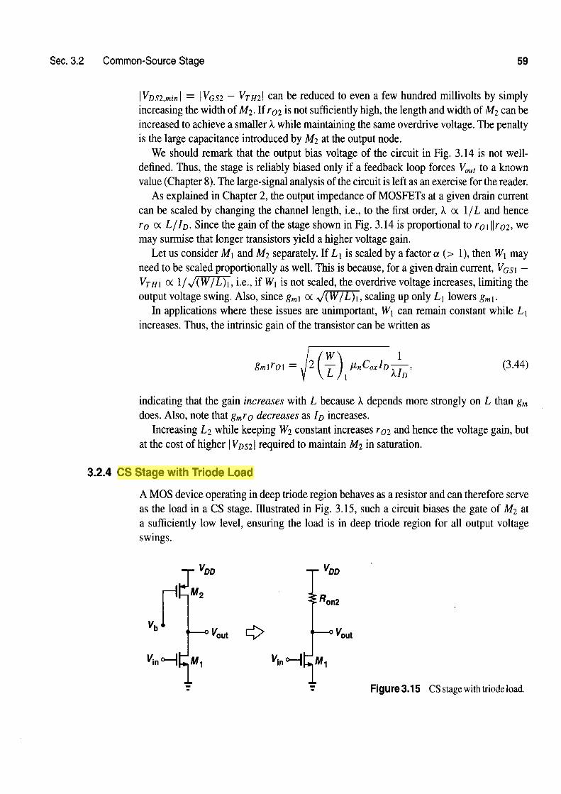
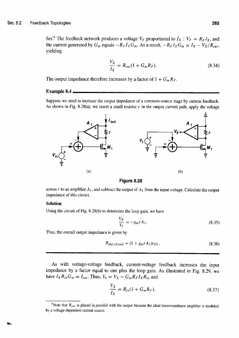
3.2.4 CS Stage with Triode Load
A MOS device operating in deep triode region behaves as a resistor and can therefore serve as the load in a CS stage. Illustrated in Fig. 3.15, such a circuit biases the gate of M2 at a sufficiently low level, ensuring the load is in deep triode region for all output voltage swings.
- - - - Figure 3.15 CS stage with triodeload.
Chap. 3 Single-Stage Amplifiers
Since
the voltage gain can be readily calculated. The principal drawback of this circuit stems from the dependence of Ron2 upon p, Cox, Vb,
and V T H P . Since ppCox and VTHP vary with process and temperature and since generating a precise value for Vb requires additional complexity, this circuit is difficult to use. Triode loads, however, consume less voltage headroom then do diode-connected devices because inFig. 3.15 Vo ,,,,,, = VDD whereas inFig. 3.12, V,,,,,,, * VDD - IVTHPJ.
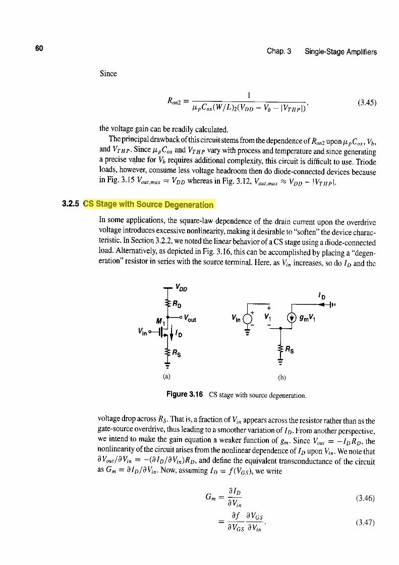
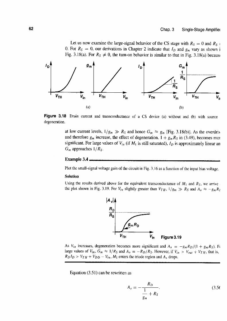
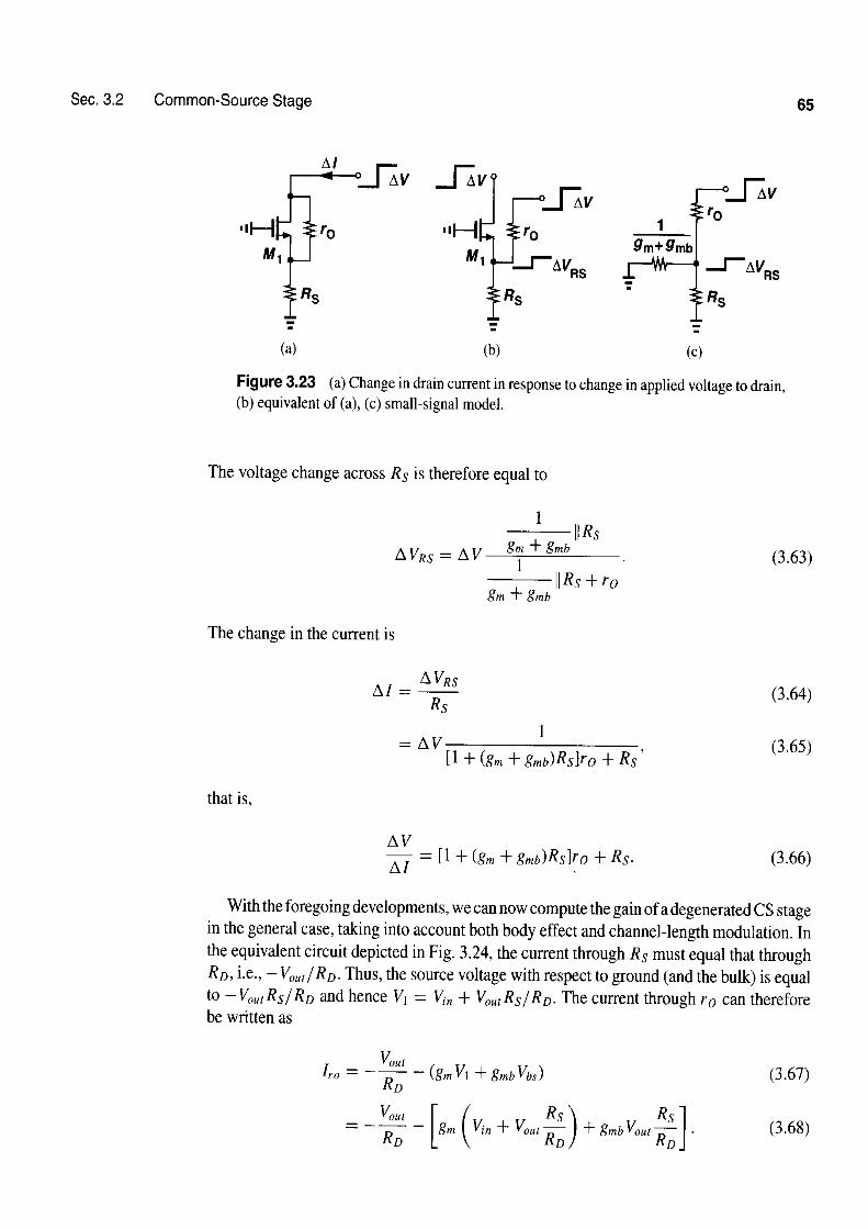
3.2.5 CS Stage with Source Degeneration
In some applications, the square-law dependence of the drain current upon the overdrive voltage introduces excessive nonlinearity, making it desirable to "soften" the device charac- teristic. In Section 3.2.2, we noted the linear behavior of a CS stage using a diode-connected load. Alternatively, as depicted in Fig. 3.16, this can be accomplished by placing a "degen- eration" resistor in series with the source terminal. Here, as Vin increases, so do I D and the
Figure 3.16 CS stage with source degeneration.
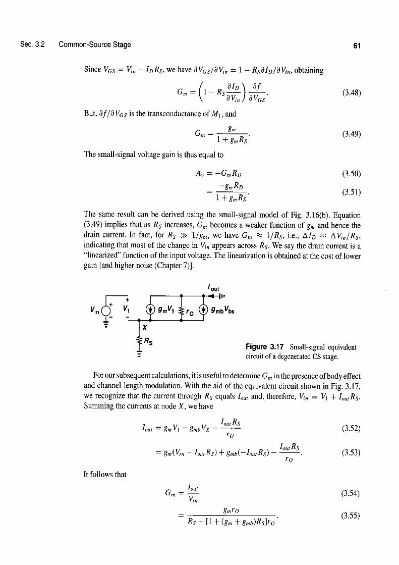
voltage drop across Rs. That is, a fraction of K n appears across the resistor rather than as the gate-source overdrive, thus leading to a smoother variation of ID. From another perspective, we intend to make the gain equation a weaker function of g,. Since V,,, = - I D R D , the nonlinearity of the circuit arises from the nonlinear dependence of ID upon Vi, . We note that aV,,,/a Vin = - (aID/aKn)RD, and define the equivalent transconductance of the circuit as G, = a ID/a K,. Now, assuming ID = f (VGS), we write
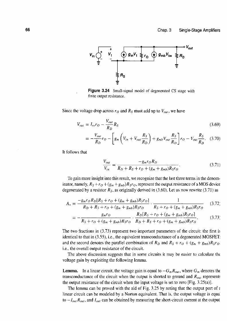
Sec. 3.3 Source Follower
Figure 3.25 Modeling output port of an amplifier by a Norton equivalent.
Defining G, = I,,, / Vin, we have V,,, = -Gm K, R,,, . This lemma proves useful if G, and R,,, can be determined by inspection.
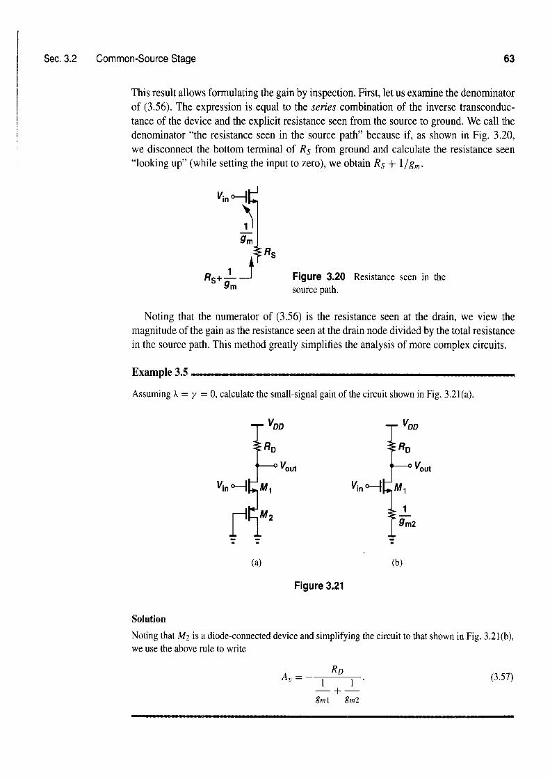
K
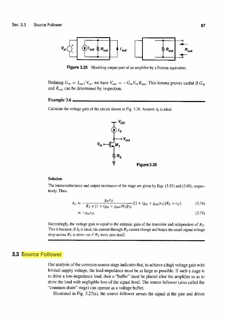
Calculate the voltage gain of the circuit shown in Fig. 3.26. Assume 10 is ideal.
I Figure 3.26
Solution
The transconductance and output resistance of the stage are given by Eqs. (3.55) and (3.60), respec- tively. Thus,
Interestingly, the voltage gain is equal to the intrinsic gain of the transistor and independent of Rs. This is because, if lo is ideal, the current through Rs cannot change and hence the small-signal voltage drop across Rs is zero-as if Rs were zero itself.
3.3 Source Follower
Our analysis of the common-source stage indicates that, to achieve a high voltage gain with limited supply voltage, the load impedance must be as large as possible. If such a stage is to drive a low-impedance load, then a "buffer" must be placed after the amplifier so as to drive the load with negligible loss of the signal level. The source follower (also called the "common-drain" stage) can operate as a voltage buffer.
Illustrated in Fig. 3.27(a), the source follower senses the signal at the gate and drives
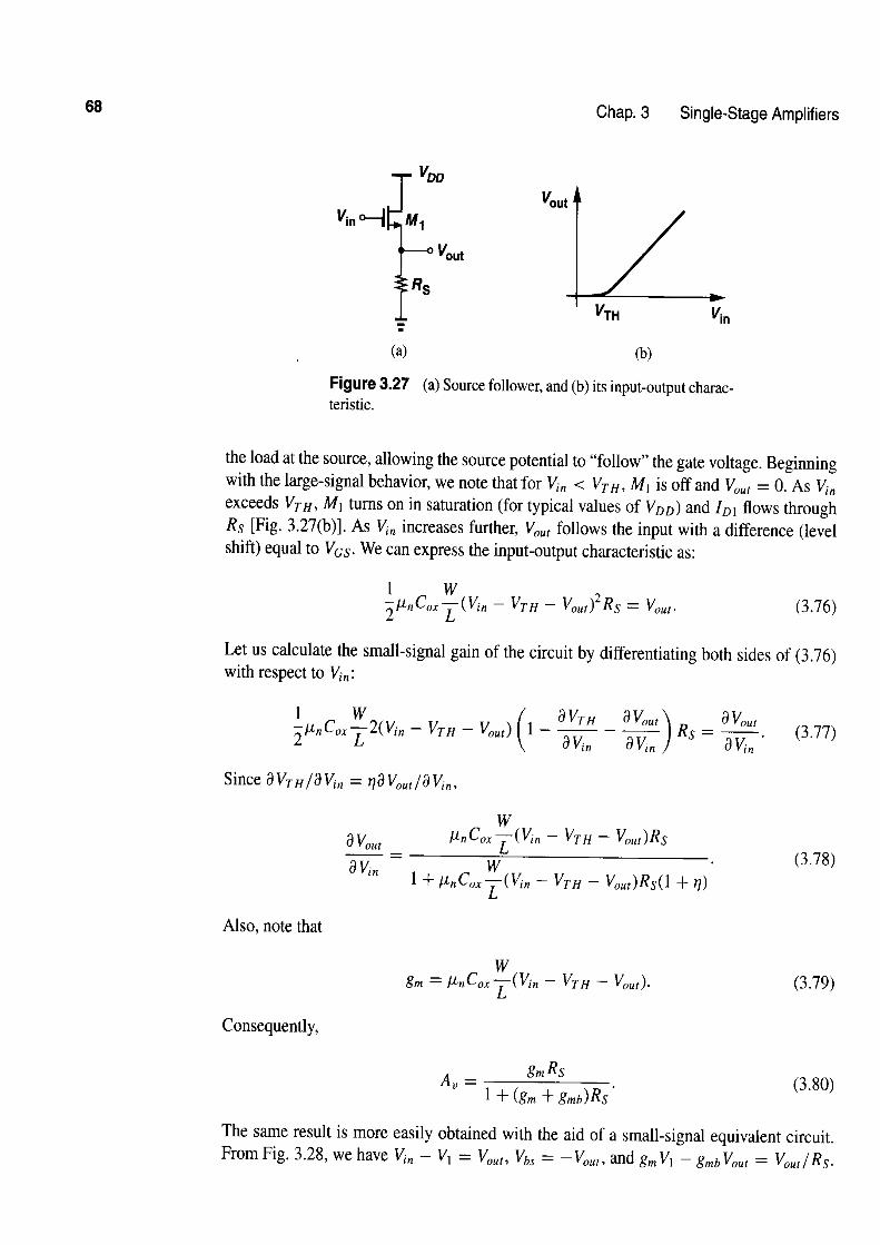
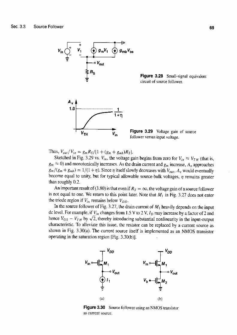
Chap. 3 Single-Stage Amplifier:
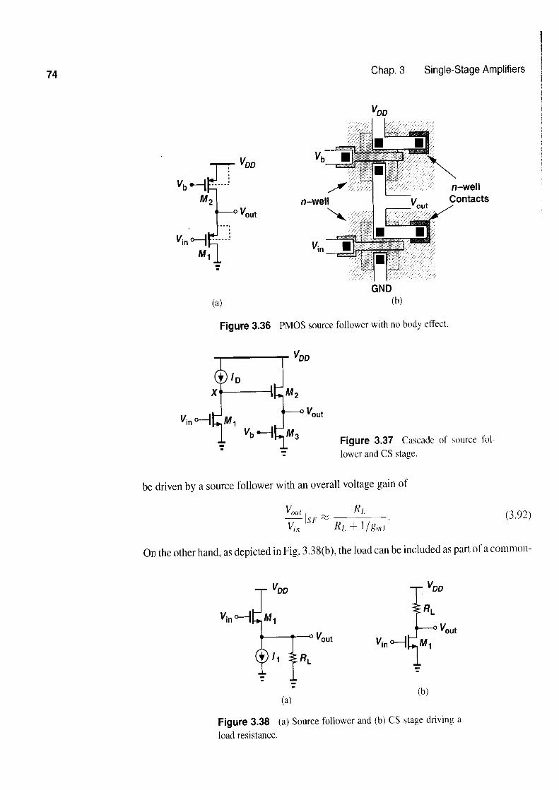
As explained in Chapter 7, source followers also introduce substantial noise. For thi: reason, the circuit of Fig. 3.39(b) is ill-suited to low-noise applications.
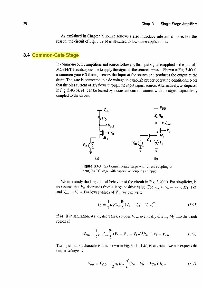
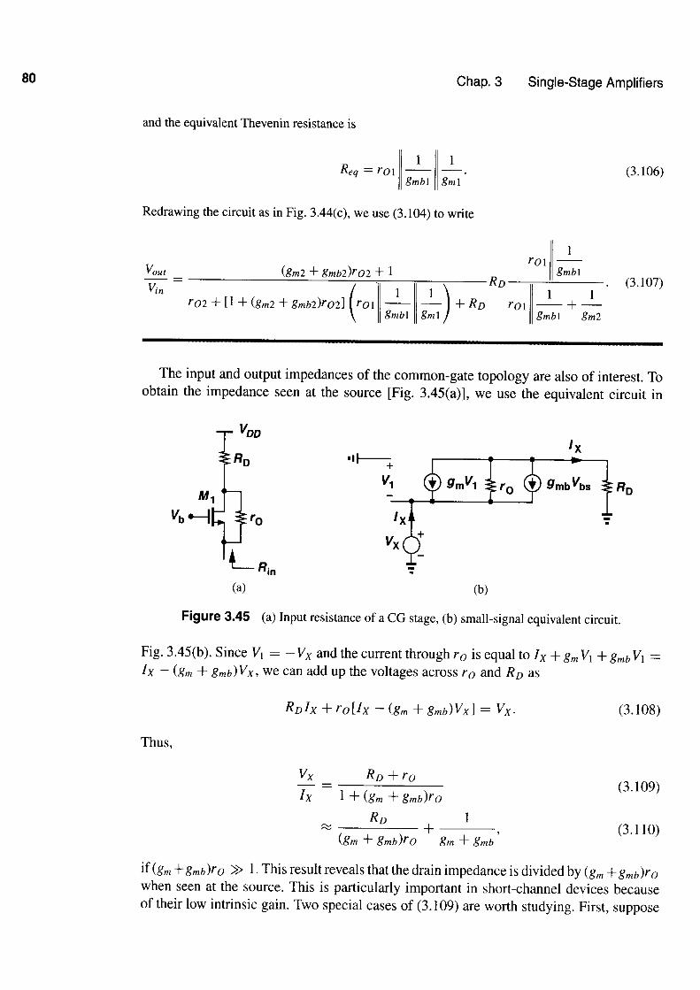
3.4 Common-Gate Stage
In common-source amplifiers and source followers, the input signal is applied to the gate of a MOSFET. It is also possible to apply the signal to the source terminal. Shown in Fig. 3.40(a). a common-gate (CG) stage senses the input at the source and produces the output at the drain. The gate is connected to a dc voltage to establish proper operating conditions. Note that thebias current of M I flows through the input signal source. Alternatively, as depicted in Fig. 3.40(b), M I can be biased by a constant current source, with the signal capacitivelq coupled to the circuit.
Figure 3.40 (a) Common-gate stage with direct coupling at input, (b) CG stage with capacitive coupling at input.
We first study the large-signal behavior of the circuit in Fig. 3.40(a). For simplicity, lel us assume that K, decreases from a large positive value. For Vin > Vb - VTH, MI is ofj and V,,, = VDD. For lower values of Vin, we can write
if M I is in saturation. As Vin decreases, so does V,,,, eventually driving M I into the triodt region if
The input-output characteristic is shown in Fig. 3.41. If M I is saturated, we can express thc output voltage as
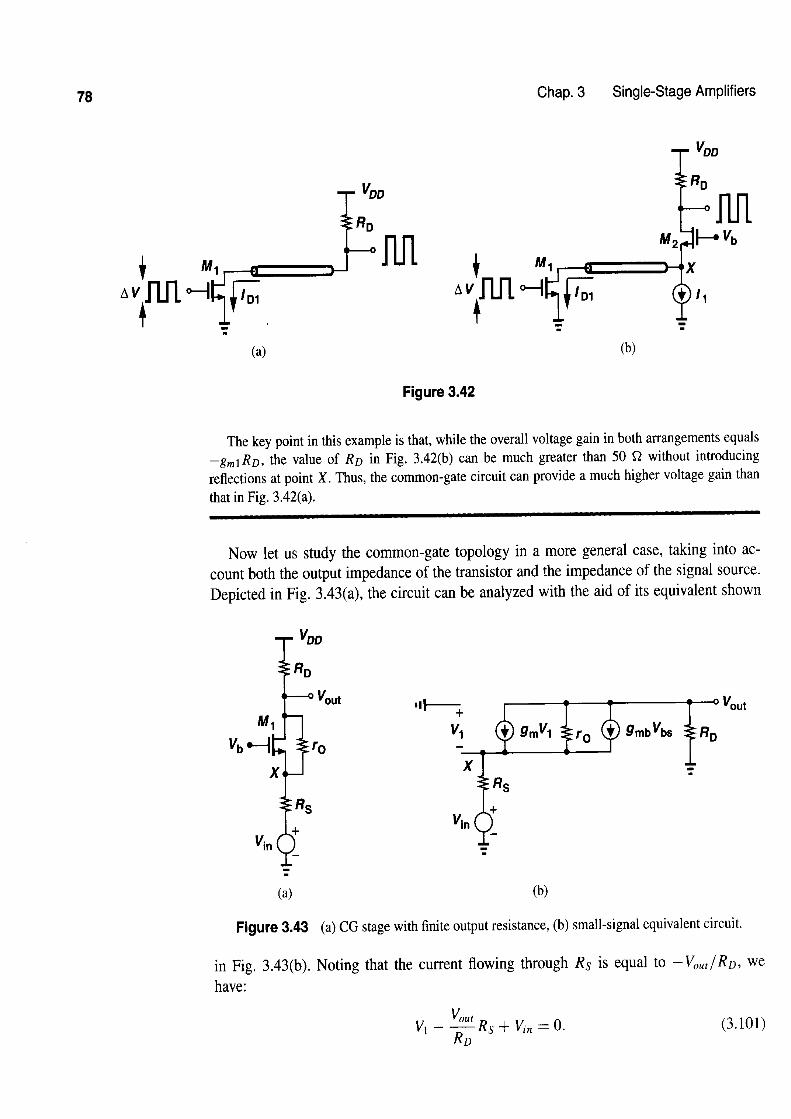
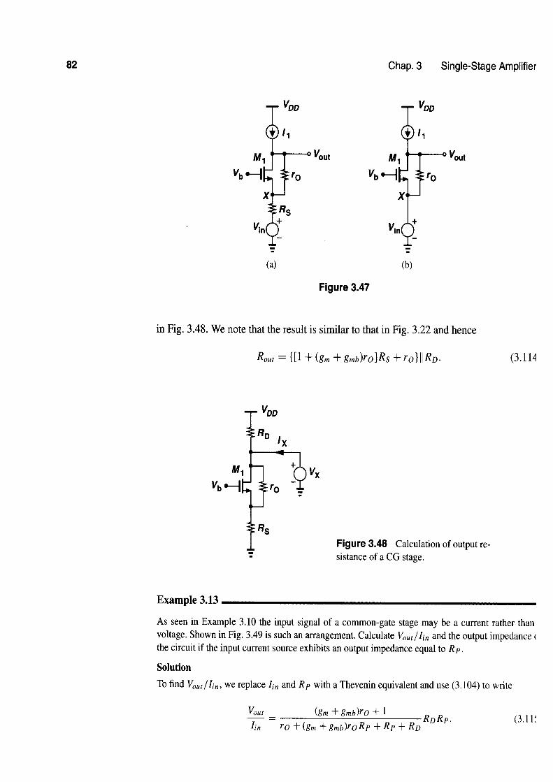
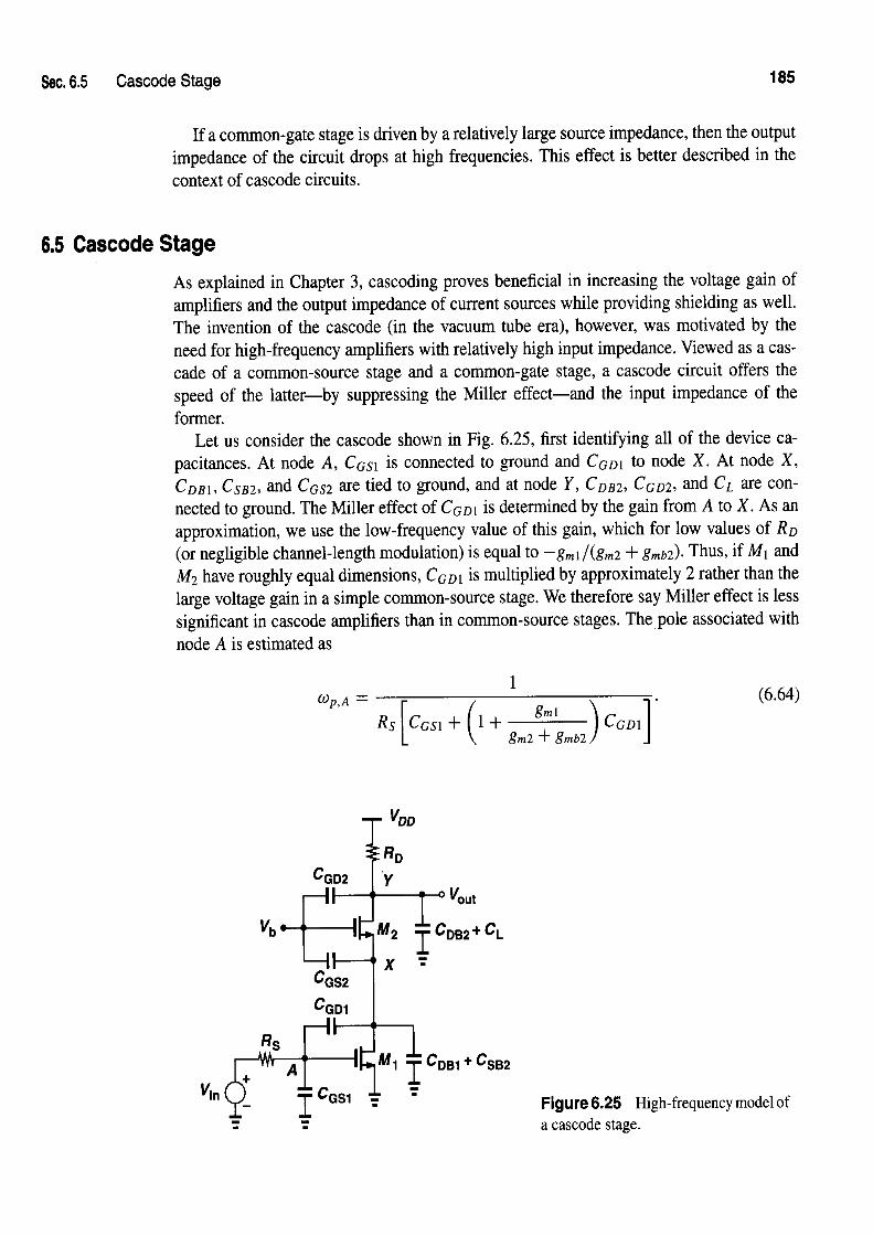
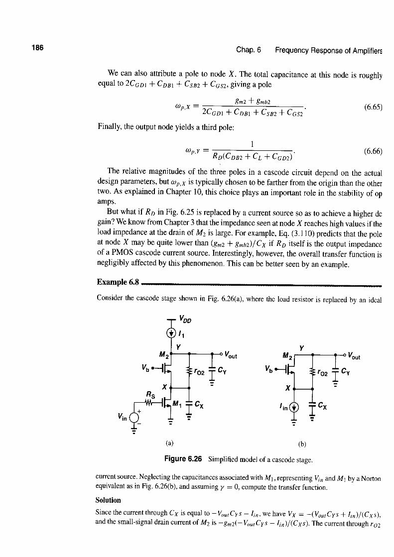
Sec. 3.5 Cascode Stage
Figure 3.49
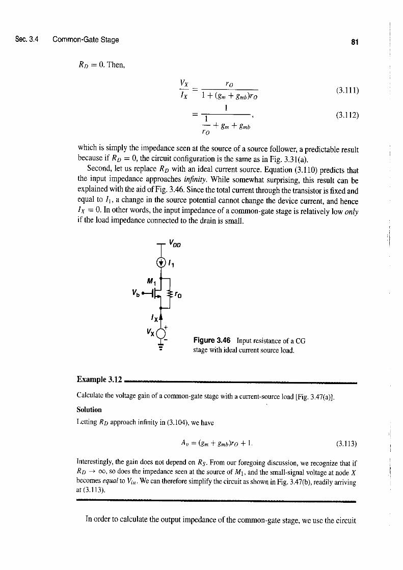
The output impedance is simply equal to
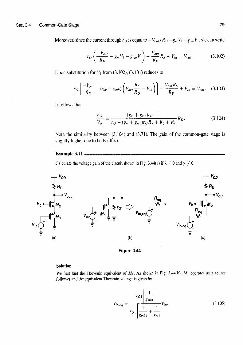
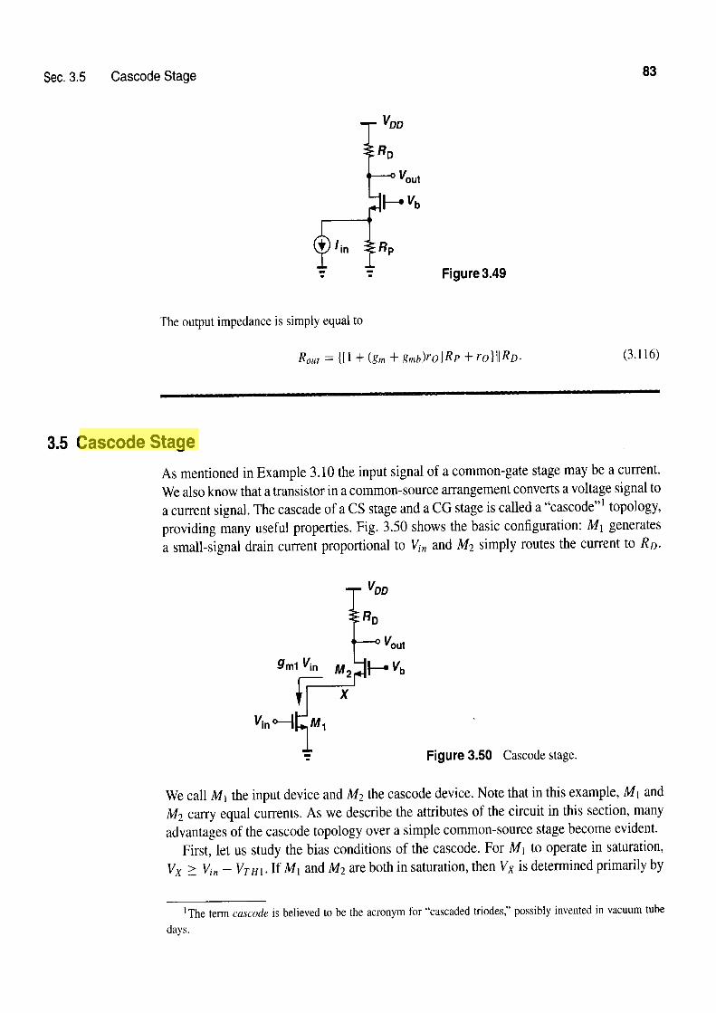
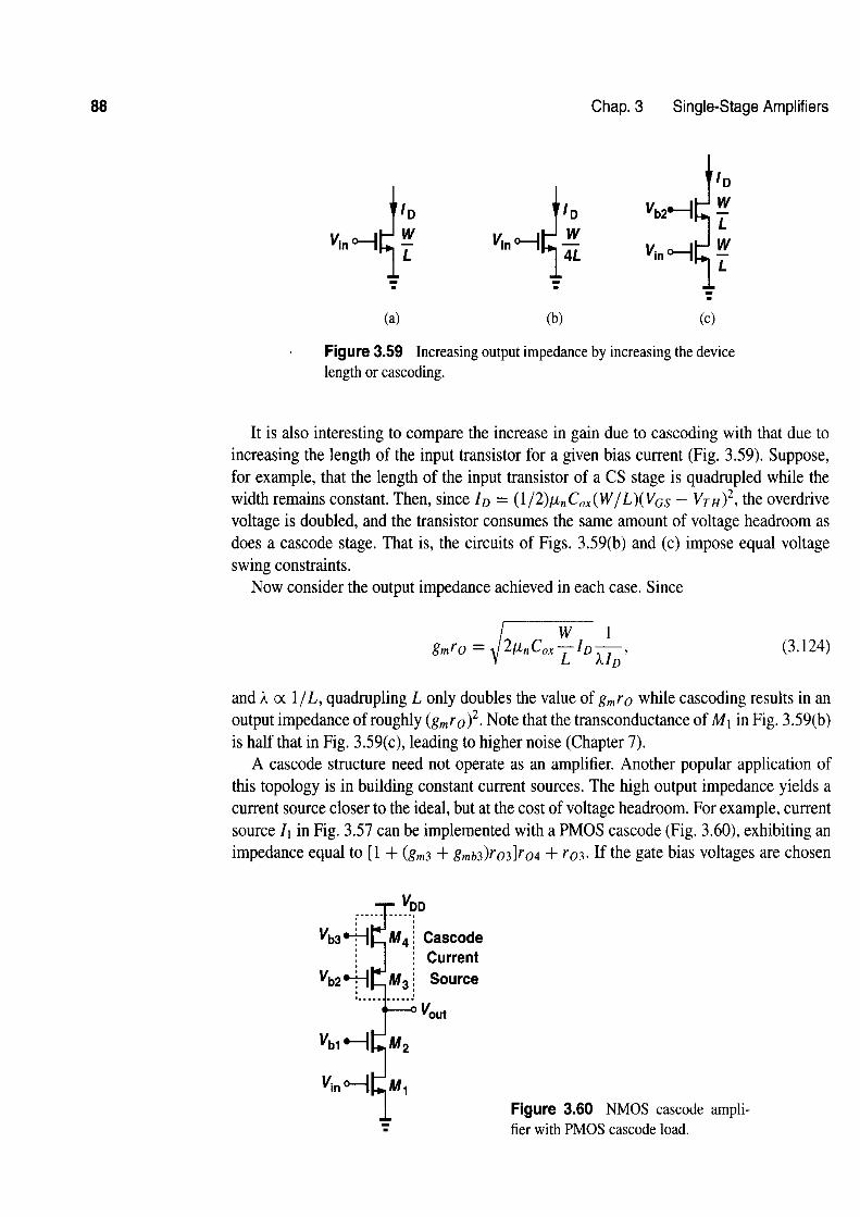
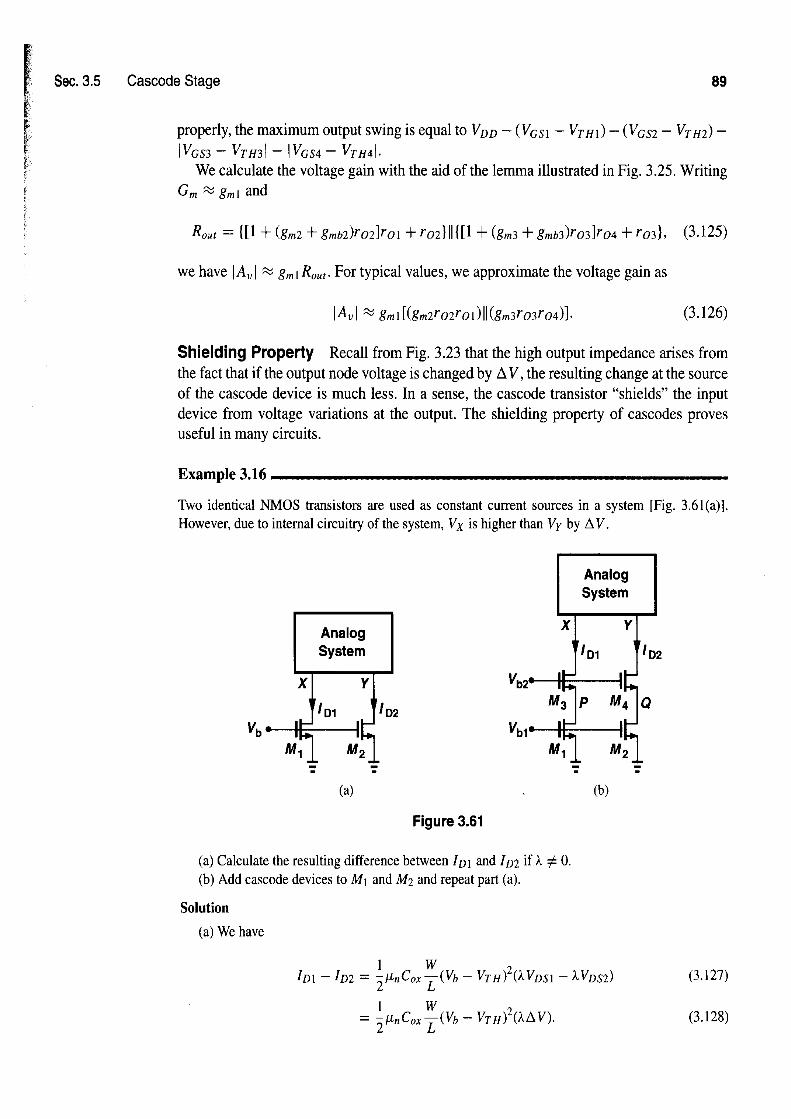
3.5 Cascode Stage
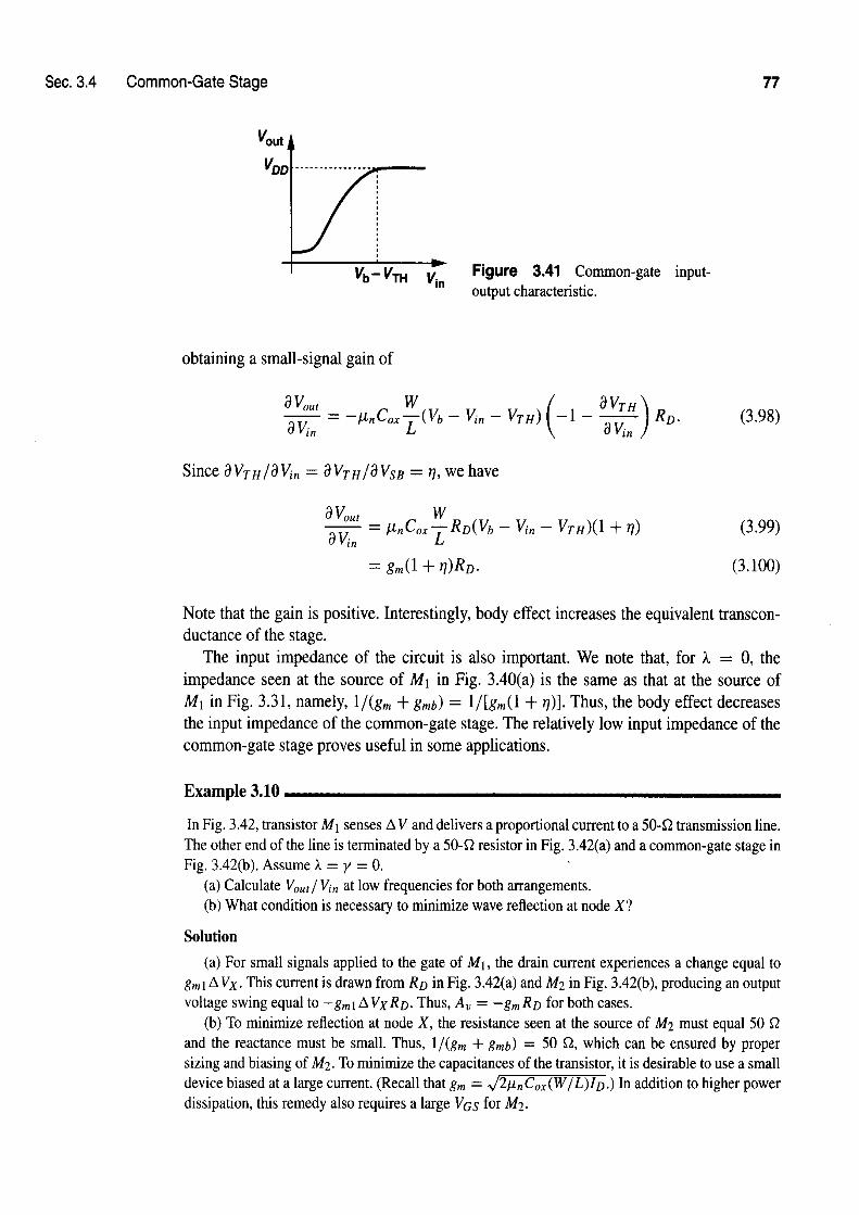
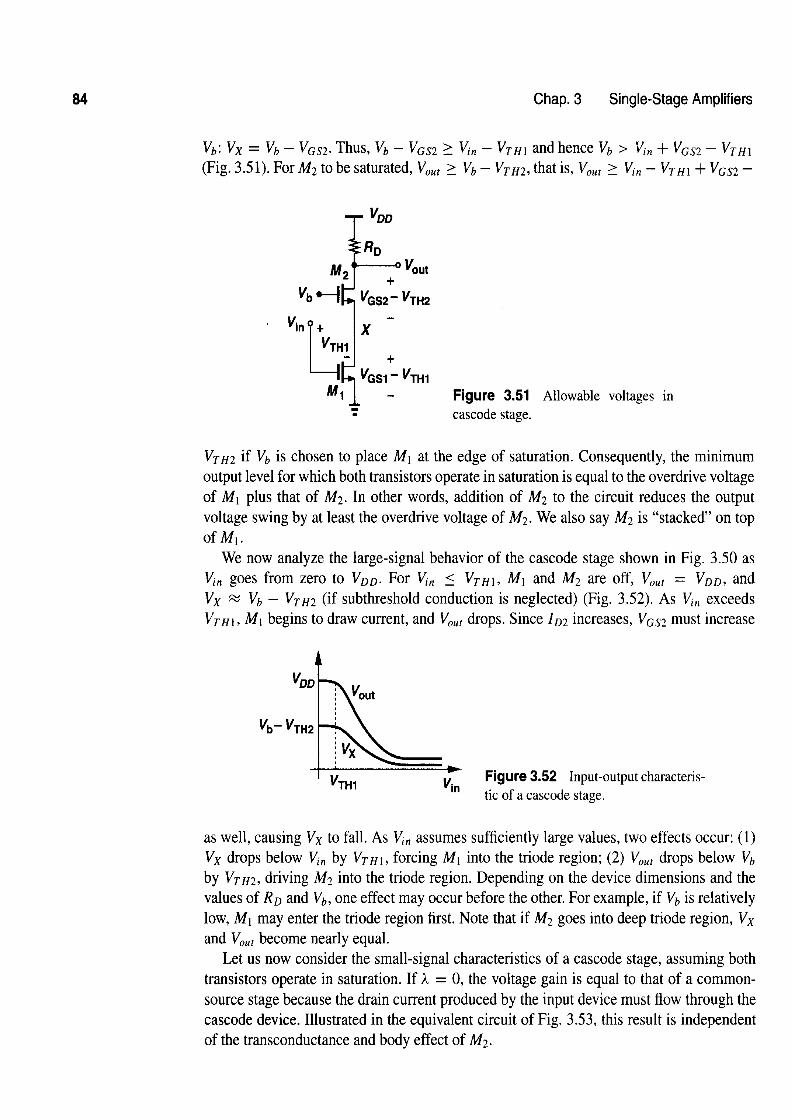
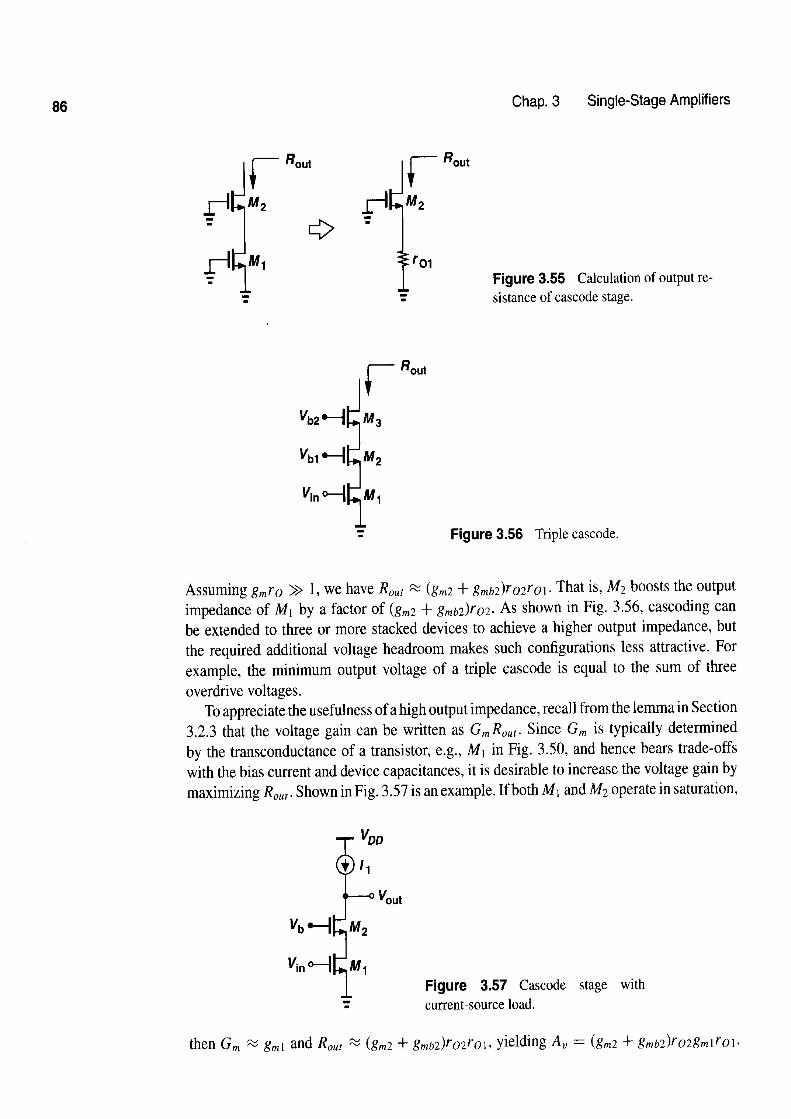
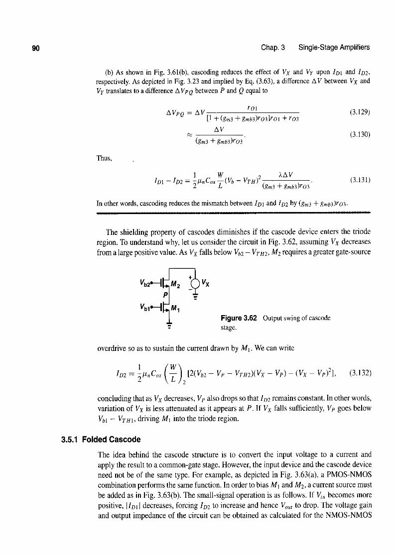
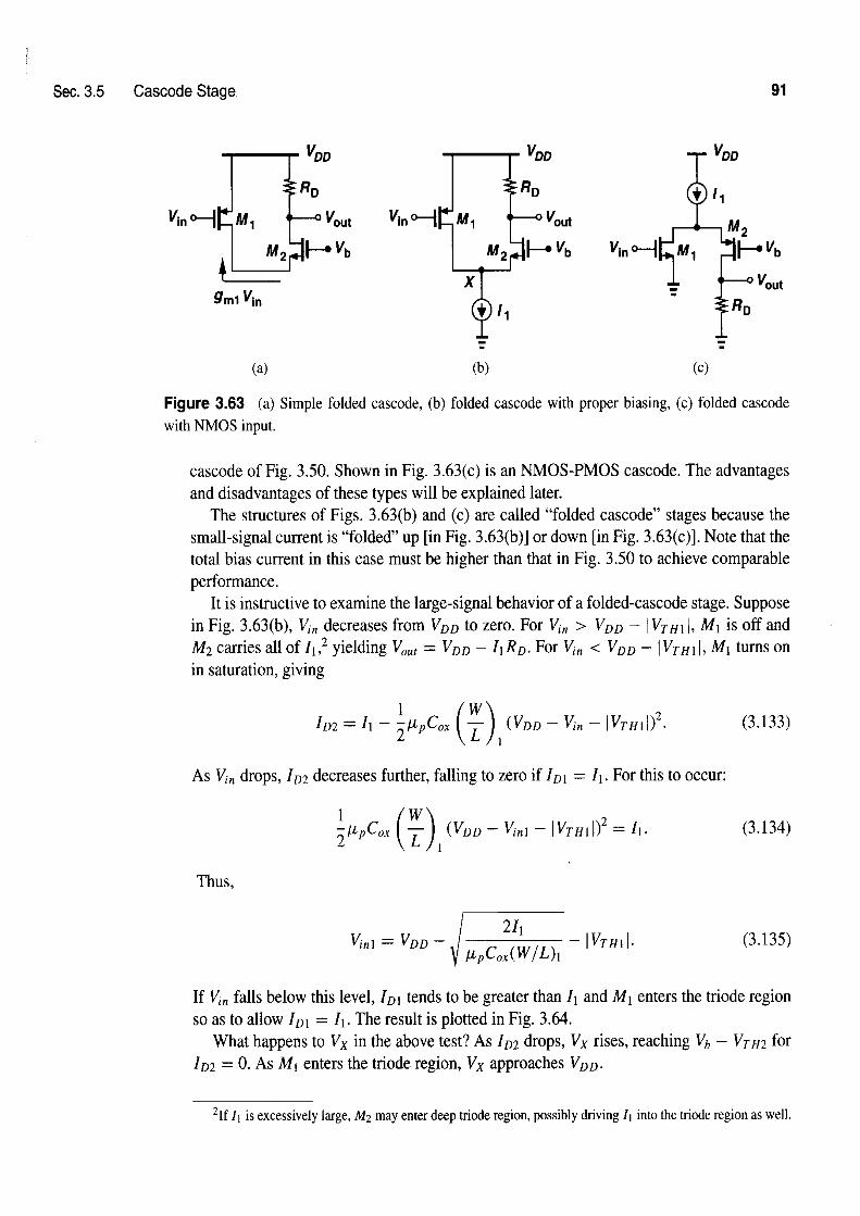
As mentioned in Example 3.10 the input signal of a common-gate stage may be a current. We also know that a transistor in a common-source arrangement converts a voltage signal to a current signal. The cascade of a CS stage and a CG stage is called a "cascode"' topology, providing many useful properties. Fig. 3.50 shows the basic configuration: M I generates a small-signal drain current proportional to &, and M2 simply routes the current to RD.
A - - Figure 3.50 Cascode stage.
We call M I the input device and M2 the cascode device. Note that in this example, M I and M2 carry equal currents. As we describe the attributes of the circuit in this section, many advantages of the cascode topology over a simple common-source stage become evident.
First, let us study the bias conditions of the cascode. For M I to operate in saturation, Vx 2 Vi, - VTHl. If M1 and M2 are both in saturation, then Vx is determined primarily by
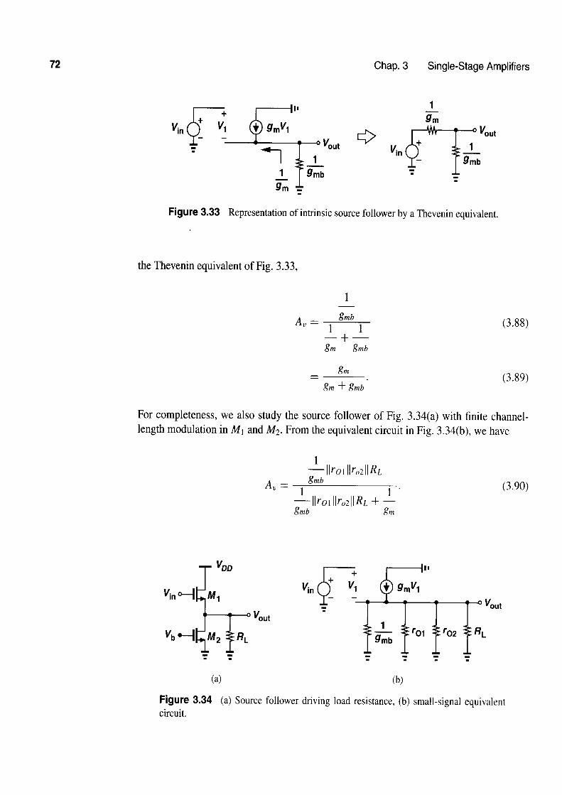
'The term cascode is believed to be the acronym for "cascaded triodes," possibly invented in vacuum tube days.
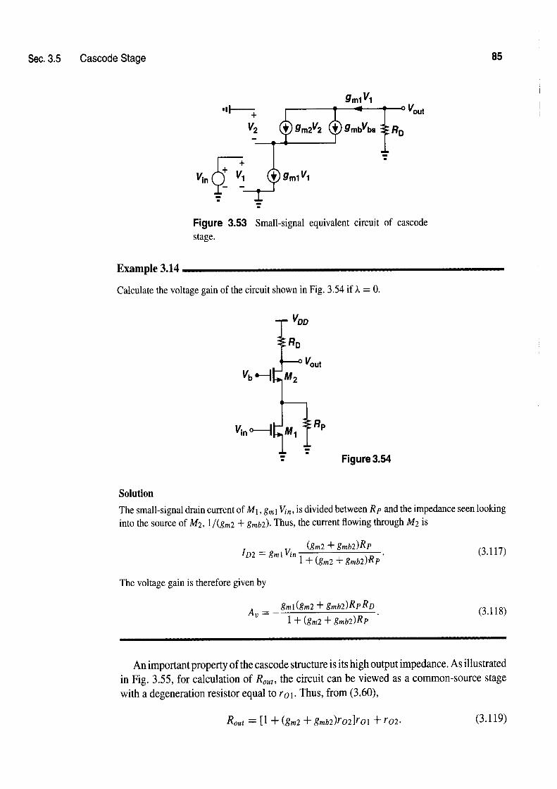


![Design of Analog CMOS Integrated Circuits [Behzad Razavi]_August 15, 2000](https://img.pdfslide.us/doc/110x75/5469f597b4af9f09638b4a61/design-of-analog-cmos-integrated-circuits-behzad-razaviaugust-15-2000.jpg)